WO2022196347A1 - 透明導電性フィルム - Google Patents
透明導電性フィルム Download PDFInfo
- Publication number
- WO2022196347A1 WO2022196347A1 PCT/JP2022/008634 JP2022008634W WO2022196347A1 WO 2022196347 A1 WO2022196347 A1 WO 2022196347A1 JP 2022008634 W JP2022008634 W JP 2022008634W WO 2022196347 A1 WO2022196347 A1 WO 2022196347A1
- Authority
- WO
- WIPO (PCT)
- Prior art keywords
- transparent conductive
- conductive layer
- film
- conductive film
- metal
- Prior art date
- Legal status (The legal status is an assumption and is not a legal conclusion. Google has not performed a legal analysis and makes no representation as to the accuracy of the status listed.)
- Ceased
Links
Images

Classifications
-
- B—PERFORMING OPERATIONS; TRANSPORTING
- B32—LAYERED PRODUCTS
- B32B—LAYERED PRODUCTS, i.e. PRODUCTS BUILT-UP OF STRATA OF FLAT OR NON-FLAT, e.g. CELLULAR OR HONEYCOMB, FORM
- B32B7/00—Layered products characterised by the relation between layers; Layered products characterised by the relative orientation of features between layers, or by the relative values of a measurable parameter between layers, i.e. products comprising layers having different physical, chemical or physicochemical properties; Layered products characterised by the interconnection of layers
- B32B7/02—Physical, chemical or physicochemical properties
- B32B7/023—Optical properties
-
- B—PERFORMING OPERATIONS; TRANSPORTING
- B32—LAYERED PRODUCTS
- B32B—LAYERED PRODUCTS, i.e. PRODUCTS BUILT-UP OF STRATA OF FLAT OR NON-FLAT, e.g. CELLULAR OR HONEYCOMB, FORM
- B32B7/00—Layered products characterised by the relation between layers; Layered products characterised by the relative orientation of features between layers, or by the relative values of a measurable parameter between layers, i.e. products comprising layers having different physical, chemical or physicochemical properties; Layered products characterised by the interconnection of layers
- B32B7/02—Physical, chemical or physicochemical properties
- B32B7/025—Electric or magnetic properties
-
- G—PHYSICS
- G06—COMPUTING OR CALCULATING; COUNTING
- G06F—ELECTRIC DIGITAL DATA PROCESSING
- G06F3/00—Input arrangements for transferring data to be processed into a form capable of being handled by the computer; Output arrangements for transferring data from processing unit to output unit, e.g. interface arrangements
- G06F3/01—Input arrangements or combined input and output arrangements for interaction between user and computer
- G06F3/03—Arrangements for converting the position or the displacement of a member into a coded form
- G06F3/041—Digitisers, e.g. for touch screens or touch pads, characterised by the transducing means
-
- H—ELECTRICITY
- H01—ELECTRIC ELEMENTS
- H01B—CABLES; CONDUCTORS; INSULATORS; SELECTION OF MATERIALS FOR THEIR CONDUCTIVE, INSULATING OR DIELECTRIC PROPERTIES
- H01B5/00—Non-insulated conductors or conductive bodies characterised by their form
- H01B5/14—Non-insulated conductors or conductive bodies characterised by their form comprising conductive layers or films on insulating-supports
Definitions
- the present invention relates to transparent conductive films.
- a transparent conductive film in which a metal oxide layer such as an indium-tin composite oxide layer (ITO layer) is formed on a resin film has been widely used as a transparent conductive film used for touch sensor electrodes and the like.
- the transparent conductive film having the metal oxide layer formed thereon has a problem that it has insufficient flexibility and cracks are likely to occur due to physical stress such as bending.
- a transparent conductive film As a transparent conductive film, a transparent conductive film having a conductive layer containing metal fibers made of silver, copper, or the like has been proposed. Such a transparent conductive film has an advantage of being excellent in flexibility. On the other hand, a conductive layer containing metal fibers has a low contact resistance, and a conductive film having the conductive layer has a problem that poor conductivity tends to occur during transportation, storage, and the like.
- the present invention has been made to solve the above problems, and an object of the present invention is to provide a transparent conductive film that has a conductive layer containing metal fibers and is less likely to cause poor conductivity due to contact. That's what it is.
- the transparent conductive film of the present invention comprises a substrate and a transparent conductive layer disposed on at least one side of the substrate, the transparent conductive layer comprising a polymer matrix and metal fibers present in the polymer matrix. and the coefficient of dynamic friction of the transparent conductive layer with respect to the transparent conductive layer is 2.0 or less.
- the metal fibers are metal nanowires.
- the metal nanowires are silver nanowires.
- the transparent conductive film further comprises a metal layer.
- the metal layer is composed of copper.
- the transparent conductive layer has a thickness of 50 nm to 300 nm.
- a transparent conductive film that has a conductive layer containing metal fibers and is less susceptible to poor conductivity due to contact.
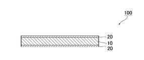
- FIG. 1 is a schematic cross-sectional view of a transparent conductive film according to one embodiment of the invention
- FIG. 4 is a schematic cross-sectional view of a transparent conductive film according to another embodiment of the invention.
- FIG. 1 is a schematic sectional view of a transparent conductive film according to one embodiment of the present invention.
- the transparent conductive film 100 includes a substrate 10 and a transparent conductive layer 20 disposed on at least one side (both sides in the illustrated example) of the substrate 10 .
- Transparent conductive layer 20 includes a polymer matrix and metal fibers present in the polymer matrix.
- the transparent conductive film may further include any other suitable layers.
- at least one outermost layer of the transparent conductive film is a transparent conductive layer.
- FIG. 2(a) and (b) are schematic cross-sectional views of a transparent conductive film according to another embodiment of the present invention.
- the transparent conductive film 200 has the transparent conductive layer 20 arranged only on one side of the substrate 10 .
- Transparent conductive film 300 further comprises metal layer 30 .
- the transparent conductive film 300 has the transparent conductive layer 20, the substrate 10, and the metal layer 30 arranged in this order.
- the coefficient of dynamic friction of the transparent conductive layer with respect to the transparent conductive layer is 2.0 or less.
- the coefficient of dynamic friction of the transparent conductive layer is 2.0 or less.
- by setting the coefficient of dynamic friction of the transparent conductive layer within the above range it is possible to obtain a transparent conductive film in which poor conductivity is unlikely to occur even when contact with the transparent conductive layer occurs.
- a conventional transparent conductive film is provided in the form of a roll, frictional force is applied to the surface by contact with each other, and when a transparent conductive layer containing metal fibers is provided, the metal fibers are separated from each other. poor conductivity is likely to occur.
- the transparent conductive film of the present invention is provided in the form of a roll, the bonding between the metal fibers is maintained and the desired conductivity is maintained.
- the transparent conductive film can exhibit excellent contact resistance not only for contact between transparent conductive films but also for contact with other articles.
- the coefficient of dynamic friction of the transparent conductive layer with respect to the transparent conductive layer is preferably 1.8 or less, more preferably 1.5 or less, still more preferably 1.2 or less, and particularly preferably 1.0 or less. and most preferably 0.8 or less. It is preferable that the coefficient of dynamic friction of the transparent conductive layer with respect to the transparent conductive layer is as small as possible, but the lower limit is, for example, 0.05.
- the “dynamic friction coefficient of the transparent conductive layer with respect to the transparent conductive layer” means the dynamic friction coefficient between the transparent conductive layer of the transparent conductive film/the transparent conductive layer of the transparent conductive film and the transparent conductive layer of the same composition.
- the coefficient of dynamic friction is measured according to JIS K7125:1999 with a measurement load of 100 g, a measurement speed of 1 mm/s, and a measurement distance of 30 mm.
- the coefficient of dynamic friction when the transparent conductive layer and the surface opposite to the transparent conductive layer are brought into contact is preferably 2.0 or less, more preferably 1.8 or less. , more preferably 1.5 or less, more preferably 1.2 or less, particularly preferably 1.0 or less, and most preferably 0.8 or less.
- the surface opposite to the transparent conductive layer means the outermost surface opposite to the surface of the transparent conductive layer to be measured with respect to the substrate.
- the transparent conductive film has a configuration of transparent conductive layer A/substrate/transparent conductive layer A
- "Dynamic friction coefficient” is the dynamic friction coefficient when the transparent conductive layers (transparent conductive layer A and transparent conductive layer A) are brought into contact with each other, and is synonymous with "dynamic friction coefficient of the transparent conductive layer with respect to the transparent conductive layer.”
- the transparent conductive film has a transparent conductive layer/substrate configuration, the “dynamic friction coefficient when the transparent conductive layer and the surface opposite to the transparent conductive layer are brought into contact” It is a dynamic friction coefficient when the conductive layer and the base material are brought into contact with each other.
- the transparent conductive film is laminated or the transparent conductive film is rolled. In this case, it is possible to remarkably prevent the occurrence of poor conduction.
- the surface resistance value of the transparent conductive film of the present invention is preferably 0.01 ⁇ /square to 1000 ⁇ /square, more preferably 0.1 ⁇ /square to 500 ⁇ /square, and particularly preferably 0.1 ⁇ /square. ⁇ 300 ⁇ /square, most preferably 0.1 ⁇ /square to 100 ⁇ /square.
- the transparent conductive film has a surface resistance value of 100 ⁇ / ⁇ or less.
- the haze value of the transparent conductive film of the present invention is preferably 1% or less, more preferably 0.7% or less, and even more preferably 0.5% or less.
- the haze value is preferably as small as possible, but its lower limit is, for example, 0.05%.
- the total light transmittance of the transparent conductive film of the present invention is preferably 80% or higher, more preferably 85% or higher, and particularly preferably 90% or higher.
- the thickness of the transparent conductive film of the present invention is preferably 10 ⁇ m to 500 ⁇ m, more preferably 15 ⁇ m to 300 ⁇ m, still more preferably 20 ⁇ m to 200 ⁇ m.
- the transparent conductive layer comprises metal fibers and a polymer matrix.
- the thickness of the transparent conductive layer is preferably 50 nm to 300 nm, more preferably 80 nm to 200 nm. By setting the thickness of the transparent conductive layer to 50 nm or more, a transparent conductive layer having a small coefficient of dynamic friction can be formed.
- the total light transmittance of the transparent conductive layer is preferably 85% or higher, more preferably 90% or higher, and still more preferably 95% or higher.
- the arithmetic mean surface roughness Ra of the transparent conductive layer is preferably 1.5 ⁇ m or more, more preferably 2.0 ⁇ m to 4.0 ⁇ m. Within such a range, a transparent conductive layer having a small coefficient of dynamic friction can be formed.
- the transparent conductive layer is patterned. Any appropriate patterning method may be employed depending on the form of the transparent conductive layer.
- the shape of the pattern of the transparent conductive layer may be any suitable shape depending on the application. For example, patterns described in JP-A-2011-511357, JP-A-2010-164938, JP-A-2008-310550, JP-A-2003-511799, and JP-A-2010-541109 can be mentioned.
- the transparent conductive layer After the transparent conductive layer is formed on the substrate, it can be patterned using any appropriate method depending on the form of the transparent conductive layer.
- Metal nanowires can be preferably used as the metal fibers.
- the metal nanowire is a conductive material made of metal, needle-like or filamentous in shape, and having a diameter of nanometers.
- the metal nanowires may be straight or curved.
- a transparent conductive layer composed of metal nanowires is used, the metal nanowires form a network, and by joining them together, a good electrical conduction path can be formed, and a transparent conductive film with low electrical resistance can be obtained. be able to.
- the ratio of the thickness d to the length L of the metal nanowires is preferably 10 to 100,000, more preferably 50 to 100,000, and particularly preferably 100 to 10,000.
- the metal nanowires having a large aspect ratio are used in this manner, the metal nanowires can cross each other satisfactorily, and a small amount of metal nanowires can exhibit high conductivity. As a result, a transparent conductive film with high light transmittance can be obtained.
- the “thickness of the metal nanowire” means the diameter when the cross section of the metal nanowire is circular, the minor axis when the metal nanowire is elliptical, and the polygonal In some cases it means the longest diagonal.
- the thickness and length of metal nanowires can be confirmed with a scanning electron microscope or a transmission electron microscope.
- the thickness of the metal nanowires is preferably less than 500 nm, more preferably less than 200 nm, particularly preferably 10 nm to 100 nm, and most preferably 10 nm to 60 nm. Within such a range, a transparent conductive layer with high light transmittance can be formed.
- the length of the metal nanowires is preferably 1 ⁇ m to 1000 ⁇ m, more preferably 1 ⁇ m to 500 ⁇ m, and particularly preferably 1 ⁇ m to 100 ⁇ m. Within such a range, a transparent conductive film with high conductivity can be obtained.
- metals constituting the metal nanowires can be used as the metal constituting the metal nanowires, as long as the metal has high conductivity.
- metals forming the metal nanowires include silver, gold, copper, and nickel. Also, materials obtained by subjecting these metals to plating (for example, gold plating) may be used.
- the metal nanowires are preferably composed of one or more metals selected from the group consisting of gold, platinum, silver and copper. In one embodiment, the metal nanowires are silver nanowires.
- any appropriate method can be adopted as the method for producing the metal nanowires. Examples include a method of reducing silver nitrate in a solution, a method of applying voltage or current from the tip of a probe to the surface of a precursor, pulling out metal nanowires at the tip of the probe, and forming the metal nanowires continuously. .
- silver nanowires can be synthesized by liquid phase reduction of a silver salt such as silver nitrate in the presence of a polyol such as ethylene glycol and polyvinylpyrrolidone. Uniformly sized silver nanowires are described, for example, in Xia, Y.; et al. , Chem. Mater. (2002), 14, 4736-4745, Xia, Y.; et al. , Nano letters (2003) 3(7), 955-960, mass production is possible.
- the content of metal nanowires in the transparent conductive layer is preferably 80% by weight or less with respect to the total weight of the transparent conductive layer. Within such a range, a transparent conductive layer having a small coefficient of dynamic friction can be formed.
- the content of the metal nanowires in the transparent conductive layer is more preferably 30 wt% to 75 wt%, more preferably 30 wt% to 65 wt%, still more preferably, relative to the total weight of the transparent conductive layer. is between 45% and 65% by weight. Within such a range, a transparent conductive film having excellent conductivity and light transmittance can be obtained.
- any appropriate polymer can be used as the polymer that constitutes the polymer matrix.
- the polymer include acrylic polymers; polyester polymers such as polyethylene terephthalate; aromatic polymers such as polystyrene, polyvinyltoluene, polyvinylxylene, polyimide, polyamide, and polyamideimide; polyurethane polymers; epoxy polymers; Polymer; acrylonitrile-butadiene-styrene copolymer (ABS); cellulose; silicon-based polymer; polyvinyl chloride; Preferably, polyfunctional compounds such as pentaerythritol triacrylate (PETA), neopentyl glycol diacrylate (NPGDA), dipentaerythritol hexaacrylate (DPHA), dipentaerythritol pentaacrylate (DPPA), trimethylolpropane triacrylate (TMPTA), etc.
- a curable resin composed of acrylate preferably an ultraviolet curable resin
- the density of the transparent conductive layer is preferably 1.3 g/cm 3 to 10.5 g/cm 3 , more preferably 1.5 g/cm 3 to 3.0 g/cm 3 . Within such a range, a transparent conductive film having excellent conductivity and light transmittance can be obtained.
- the transparent conductive layer is formed by applying a conductive layer-forming composition containing metal fibers (for example, metal nanowires) to the substrate (or a laminate of the substrate and other layers), and then drying the coated layer.
- the conductive layer-forming composition may contain a resin material that forms a polymer matrix.
- a resin material that forms the polymer matrix is prepared separately from the conductive layer-forming composition, and after the conductive layer-forming composition is applied and dried, the resin material (polymer composition material, monomer composition) and then drying or curing the applied layer of the resin material to form a transparent conductive layer.
- the composition for forming a conductive layer may contain metal fibers (for example, metal nanowires) as well as any suitable solvent.
- the conductive layer-forming composition may be prepared as a dispersion of metal fibers (eg, metal nanowires).
- the solvent include water, alcohol solvents, ketone solvents, ether solvents, hydrocarbon solvents, aromatic solvents and the like. From the viewpoint of reducing environmental load, it is preferable to use water.
- the conductive layer-forming composition may further contain any appropriate additive depending on the purpose. Examples of the additive include corrosion inhibitors that prevent corrosion of metal fibers (eg, metal nanowires), surfactants that prevent aggregation of metal fibers (eg, metal nanowires), and the like. The type, number and amount of additives used can be appropriately set according to the purpose.
- the dispersion concentration of the metal fibers (eg, metal nanowires) in the conductive layer-forming composition is preferably 0.1% by weight to 1% by weight. Within such a range, a transparent conductive layer having excellent conductivity and light transmittance can be formed.
- any appropriate method can be adopted as a method for applying the conductive layer-forming composition.
- coating methods include spray coating, bar coating, roll coating, die coating, inkjet coating, screen coating, dip coating, letterpress printing, intaglio printing, and gravure printing.
- Any appropriate drying method (for example, natural drying, air drying, heat drying) may be employed as a drying method for the coating layer.
- the drying temperature is typically 50°C to 200°C, preferably 80°C to 150°C. Drying times are typically 1 to 10 minutes.
- the polymer solution contains a polymer that constitutes the polymer matrix or a precursor of the polymer (a monomer that constitutes the polymer).
- the polymer solution may contain a solvent.
- the solvent contained in the polymer solution include alcohol-based solvents, ketone-based solvents, tetrahydrofuran, hydrocarbon-based solvents, aromatic solvents, and the like.
- the solvent is volatile.
- the boiling point of the solvent is preferably 200° C. or lower, more preferably 150° C. or lower, and still more preferably 100° C. or lower.
- the substrate is typically composed of any suitable resin.
- the resin constituting the substrate include cycloolefin-based resin, polyimide-based resin, polyvinylidene chloride-based resin, polyvinyl chloride-based resin, polyethylene terephthalate-based resin, polyethylene naphthalate-based resin, and the like. Cycloolefin resins are preferably used. A transparent conductive film having excellent flexibility can be obtained by using a substrate composed of a cycloolefin resin.
- polynorbornene can be preferably used as the cycloolefin-based resin.
- Polynorbornene refers to a (co)polymer obtained by using a norbornene-based monomer having a norbornene ring as part or all of the starting material (monomer).
- Various products are commercially available as polynorbornene. Specific examples include the trade names “Zeonex” and “Zeonor” manufactured by Zeon Corporation, the trade name “Arton” manufactured by JSR Corporation, the trade name “Topas” manufactured by TICONA, and the trade name manufactured by Mitsui Chemicals. "APEL" may be mentioned.
- the glass transition temperature of the resin constituting the base material is preferably 50°C to 200°C, more preferably 60°C to 180°C, and still more preferably 70°C to 160°C.
- a substrate having a glass transition temperature within such a range can prevent deterioration during formation of a transparent conductive laminate.
- the thickness of the base material is preferably 8 ⁇ m to 500 ⁇ m, more preferably 10 ⁇ m to 250 ⁇ m, even more preferably 10 ⁇ m to 150 ⁇ m, and particularly preferably 15 ⁇ m to 100 ⁇ m.
- the total light transmittance of the substrate is preferably 80% or higher, more preferably 85% or higher, and particularly preferably 90% or higher. Within such a range, a transparent conductive film suitable as a transparent conductive film provided in a touch panel or the like can be obtained.
- the base material may further contain any suitable additive as necessary.
- additives include plasticizers, heat stabilizers, light stabilizers, lubricants, antioxidants, UV absorbers, flame retardants, colorants, antistatic agents, compatibilizers, cross-linking agents, and thickeners. etc.
- the type and amount of additive used can be appropriately set according to the purpose.
- the base material may be any appropriate method is adopted for the surface treatment depending on the purpose. Examples include low-pressure plasma treatment, ultraviolet irradiation treatment, corona treatment, flame treatment, acid or alkali treatment.
- the transparent substrate is surface-treated to make the transparent substrate surface hydrophilic.
- the base material hydrophilic By making the base material hydrophilic, the workability is excellent when the composition for forming a transparent conductive layer prepared with an aqueous solvent is applied. Also, a transparent conductive film having excellent adhesion between the substrate and the transparent conductive layer can be obtained.
- the metal layer is composed of any suitable metal. Preferably, it is composed of a conductive metal such as silver, gold, copper or nickel. In one embodiment, the metal layer is composed of copper.
- the metal layer can be formed by any appropriate method.
- the metal layer can be formed by a vapor deposition method, a sputtering method, a dry process (dry method) such as CVD, a wet process such as plating, or the like.
- IPA isopropanol
- DAA diacetone alcohol
- a transparent conductive layer A was formed by irradiating ultraviolet light with an exposure amount of 450 mJ/cm 2 to obtain a transparent conductive film A consisting of a substrate/transparent conductive layer A.
- the transparent conductive film A was subjected to the following evaluations.
- the surface resistance value of the transparent conductive layer was measured with a non-contact surface resistance measuring instrument (manufactured by NAPSON, trade name "EC-80", sheet resistance measurement mode, room temperature: 26°C) for the above-mentioned sliding portion and other portions. was measured using The rate of increase in resistance value due to sliding was determined by the formula: (Surface resistance value of slidable portion/Surface resistance value of other than slidable portion). (4) Arithmetic mean roughness Ra of transparent conductive layer A Using a scanning probe microscope "Nanoscope IV" AFM tapping mode manufactured by Veeco Instruments, the arithmetic mean roughness Ra in a 5 ⁇ m ⁇ 5 ⁇ m region of the surface of the transparent conductive layer A was measured.
- Example 1-1 A transparent conductive film A was obtained in the same manner as in Example 1.
- (1a) Dynamic Friction Coefficient with respect to Copper Film on Transparent Conductive Layer A Separately, in the same manner as in Example 1, a transparent conductive film A was obtained. A copper film having a thickness of 100 nm was formed by sputtering on the transparent conductive layer A of the obtained transparent conductive film A to obtain a transparent conductive film with a copper film. Using this transparent conductive film with a copper film as a sample on the contact side, the transparent conductive layer A and the copper film on the transparent conductive layer A are slid in the same manner as in (1) above, and the dynamic friction coefficient is measured. did.
- Example 1-2 A transparent conductive film A was obtained in the same manner as in Example 1. (1b) Coefficient of dynamic friction with respect to transparent conductive layer d
- the silver nanowire ink obtained in Production Example 1 is applied on a base material (cycloolefin film) using a wire bar, and the specific resistance value after film formation is 50 ⁇ / ⁇ . and heated at 120° C. for 2 minutes to form a film.
- a photocurable resin containing urethane acrylate as a main component is diluted with methyl isobutyl ketone to a solid content concentration of 1.5% to prepare a coating liquid a, and a spin coater is used to dry the silver nanowire ink coated surface.
- Example 1-3 A transparent conductive film A was obtained in the same manner as in Example 1.
- (1c) Dynamic Friction Coefficient for Cycloolefin Film A cycloolefin film (manufactured by Nippon Zeon Co., Ltd., trade name “ZF16”) was used as a sample on the contactor side, and the transparent conductive layer A and the cycloolefin film were treated in the same manner as in (1) above. and the dynamic friction coefficient was measured.
- Example 1-4 A transparent conductive film A was obtained in the same manner as in Example 1.
- Example 1-5 A transparent conductive film A was obtained in the same manner as in Example 1.
- Example 2 A transparent conductive film B consisting of a substrate/transparent conductive layer B was obtained in the same manner as in Example 1, except that the dry film thickness of the coating solution a was 100 nm. Transparent conductive film B was subjected to the following evaluations.
- the surface resistance value of the transparent conductive layer was measured with a non-contact surface resistance measuring instrument (manufactured by NAPSON, trade name "EC-80", sheet resistance measurement mode, room temperature: 26°C) for the above-mentioned sliding portion and other portions. was measured using The rate of increase in resistance value due to sliding was determined by the formula: (Surface resistance value of slidable portion/Surface resistance value of other than slidable portion). (4B) Arithmetic mean roughness Ra of transparent conductive layer B Using a scanning probe microscope "Nanoscope IV" AFM tapping mode manufactured by Veeco Instruments, the arithmetic mean roughness Ra in a 5 ⁇ m ⁇ 5 ⁇ m region on the surface of the transparent conductive layer B was measured.
- Example 1 A silver nanowire layer was formed in the same manner as in Example 1. Furthermore, a silane coupling agent is added to a photocurable resin containing urethane acrylate as a main component, and a coating liquid c is prepared by diluting with methyl isobutyl ketone to a solid content concentration of 1.5%. It was applied using a spin coater so that the dry film thickness was 70 nm, heated at 80° C. for 1 minute, and then irradiated with ultraviolet rays with an integrated exposure amount of 450 mJ/cm 2 from a high-pressure mercury lamp to form a transparent conductive layer C. , a transparent conductive film C consisting of a base material/transparent conductive film C was obtained.
- a transparent conductive film d comprising a substrate/transparent conductive layer d was obtained in the same manner as described in Reference Example 1-2.
- (1g) Dynamic Friction Coefficient with respect to Transparent Conductive Layer d Using the transparent conductive layer d as the sample on the contact side, the transparent conductive layer d and the transparent conductive layer d are slid in the same manner as in (1) above, and the dynamic friction coefficient is was measured.
- (2g) Static friction coefficient Using the transparent conductive layer d as the sample on the contact side, the transparent conductive layer d and the transparent conductive layer d are slid in the same manner as in (2) above, and the coefficient of friction at the start of sliding (static friction coefficient ) was measured.
- Table 1 shows the evaluation results of the above Examples, Reference Examples, Comparative Examples, and Comparative Reference Examples.
- the sample on the side of the contact in terms of the coefficient of dynamic friction and rate of increase in resistance value is described as "the layer brought into contact with the transparent conductive layer" in the table.
- the coefficient of dynamic friction of the transparent conductive layer with respect to the transparent conductive layer is set to 2.0 or less. It is possible to provide a transparent conductive film in which defects are unlikely to occur. As shown in Reference Examples, such a transparent conductive film suppresses an increase in resistance value even when it is brought into contact with and slid on various films.
Landscapes
- Engineering & Computer Science (AREA)
- General Engineering & Computer Science (AREA)
- Theoretical Computer Science (AREA)
- Human Computer Interaction (AREA)
- Physics & Mathematics (AREA)
- General Physics & Mathematics (AREA)
- Non-Insulated Conductors (AREA)
- Laminated Bodies (AREA)
Priority Applications (2)
| Application Number | Priority Date | Filing Date | Title |
|---|---|---|---|
| CN202280021396.0A CN117015834A (zh) | 2021-03-18 | 2022-03-01 | 透明导电性膜 |
| KR1020237030713A KR102843527B1 (ko) | 2021-03-18 | 2022-03-01 | 투명 도전성 필름 |
Applications Claiming Priority (2)
| Application Number | Priority Date | Filing Date | Title |
|---|---|---|---|
| JP2021-044561 | 2021-03-18 | ||
| JP2021044561A JP7485629B2 (ja) | 2021-03-18 | 2021-03-18 | 透明導電性フィルム |
Publications (1)
| Publication Number | Publication Date |
|---|---|
| WO2022196347A1 true WO2022196347A1 (ja) | 2022-09-22 |
Family
ID=83321497
Family Applications (1)
| Application Number | Title | Priority Date | Filing Date |
|---|---|---|---|
| PCT/JP2022/008634 Ceased WO2022196347A1 (ja) | 2021-03-18 | 2022-03-01 | 透明導電性フィルム |
Country Status (5)
| Country | Link |
|---|---|
| JP (1) | JP7485629B2 (https=) |
| KR (1) | KR102843527B1 (https=) |
| CN (1) | CN117015834A (https=) |
| TW (1) | TW202244946A (https=) |
| WO (1) | WO2022196347A1 (https=) |
Citations (2)
| Publication number | Priority date | Publication date | Assignee | Title |
|---|---|---|---|---|
| JP2018135492A (ja) * | 2017-02-23 | 2018-08-30 | ナガセケムテックス株式会社 | 透明導電膜、透明導電積層体、立体形状ディスプレイ及び樹脂組成物 |
| JP2021037668A (ja) * | 2019-09-02 | 2021-03-11 | 日東電工株式会社 | 透明導電性フィルム、透明導電性フィルムの製造方法および中間体 |
Family Cites Families (3)
| Publication number | Priority date | Publication date | Assignee | Title |
|---|---|---|---|---|
| ATE532217T1 (de) | 2005-08-12 | 2011-11-15 | Cambrios Technologies Corp | Verfahren zur herstellung von transparente leiter auf nanodrahtbasis |
| CN103167993B (zh) | 2010-10-07 | 2015-08-19 | 电气化学工业株式会社 | 电子器件包装用片材及其成型体 |
| WO2012133367A1 (ja) | 2011-03-28 | 2012-10-04 | 東レ株式会社 | 導電積層体およびタッチパネル |
-
2021
- 2021-03-18 JP JP2021044561A patent/JP7485629B2/ja active Active
-
2022
- 2022-03-01 CN CN202280021396.0A patent/CN117015834A/zh active Pending
- 2022-03-01 KR KR1020237030713A patent/KR102843527B1/ko active Active
- 2022-03-01 WO PCT/JP2022/008634 patent/WO2022196347A1/ja not_active Ceased
- 2022-03-07 TW TW111108174A patent/TW202244946A/zh unknown
Patent Citations (2)
| Publication number | Priority date | Publication date | Assignee | Title |
|---|---|---|---|---|
| JP2018135492A (ja) * | 2017-02-23 | 2018-08-30 | ナガセケムテックス株式会社 | 透明導電膜、透明導電積層体、立体形状ディスプレイ及び樹脂組成物 |
| JP2021037668A (ja) * | 2019-09-02 | 2021-03-11 | 日東電工株式会社 | 透明導電性フィルム、透明導電性フィルムの製造方法および中間体 |
Also Published As
| Publication number | Publication date |
|---|---|
| JP2022143835A (ja) | 2022-10-03 |
| KR102843527B1 (ko) | 2025-08-07 |
| KR20230142601A (ko) | 2023-10-11 |
| JP7485629B2 (ja) | 2024-05-16 |
| CN117015834A (zh) | 2023-11-07 |
| TW202244946A (zh) | 2022-11-16 |
Similar Documents
| Publication | Publication Date | Title |
|---|---|---|
| TWI450282B (zh) | Transparent conductive film with adhesive layer and manufacturing method thereof | |
| JP2012151095A (ja) | 透明導電性フィルム、静電容量式タッチパネルの透明電極及びタッチパネル | |
| JPWO2013047493A1 (ja) | 透明導電層付き基体及びその製造方法 | |
| WO2022050243A1 (ja) | 透明導電性フィルムの製造方法 | |
| WO2022196347A1 (ja) | 透明導電性フィルム | |
| WO2022196348A1 (ja) | 透明導電性フィルム | |
| WO2022172870A1 (ja) | 透明導電性フィルム | |
| JP2002347150A (ja) | 機能性層を有する機能性フィルム及びその機能性層が付与された物体 | |
| WO2016163364A1 (ja) | 導電性積層体、タッチパネル及び導電性積層体の製造方法 | |
| JP2023127683A (ja) | 透明導電性フィルムの製造方法 | |
| JP2014238930A (ja) | 透明導電性フィルムの製造方法 | |
| TWI890831B (zh) | 透明導電性膜 | |
| JP7719722B2 (ja) | 透明導電性フィルムの製造方法 | |
| TWI918653B (zh) | 透明導電性膜 | |
| WO2021235430A1 (ja) | 透明導電性フィルム | |
| KR20230013634A (ko) | 도전성 필름 | |
| TWI709149B (zh) | 包括金屬跡線之透明導體及其製造方法 | |
| JP2023183132A (ja) | 透明導電性フィルム |
Legal Events
| Date | Code | Title | Description |
|---|---|---|---|
| 121 | Ep: the epo has been informed by wipo that ep was designated in this application |
Ref document number: 22771101 Country of ref document: EP Kind code of ref document: A1 |
|
| ENP | Entry into the national phase |
Ref document number: 20237030713 Country of ref document: KR Kind code of ref document: A |
|
| WWE | Wipo information: entry into national phase |
Ref document number: 1020237030713 Country of ref document: KR |
|
| WWE | Wipo information: entry into national phase |
Ref document number: 202280021396.0 Country of ref document: CN |
|
| NENP | Non-entry into the national phase |
Ref country code: DE |
|
| 122 | Ep: pct application non-entry in european phase |
Ref document number: 22771101 Country of ref document: EP Kind code of ref document: A1 |