WO2022190729A1 - 積層圧電素子 - Google Patents
積層圧電素子 Download PDFInfo
- Publication number
- WO2022190729A1 WO2022190729A1 PCT/JP2022/004356 JP2022004356W WO2022190729A1 WO 2022190729 A1 WO2022190729 A1 WO 2022190729A1 JP 2022004356 W JP2022004356 W JP 2022004356W WO 2022190729 A1 WO2022190729 A1 WO 2022190729A1
- Authority
- WO
- WIPO (PCT)
- Prior art keywords
- piezoelectric
- layer
- piezoelectric element
- electrode layer
- laminated
- Prior art date
- Legal status (The legal status is an assumption and is not a legal conclusion. Google has not performed a legal analysis and makes no representation as to the accuracy of the status listed.)
- Ceased
Links
Images


Classifications
-
- H—ELECTRICITY
- H10—SEMICONDUCTOR DEVICES; ELECTRIC SOLID-STATE DEVICES NOT OTHERWISE PROVIDED FOR
- H10N—ELECTRIC SOLID-STATE DEVICES NOT OTHERWISE PROVIDED FOR
- H10N30/00—Piezoelectric or electrostrictive devices
- H10N30/50—Piezoelectric or electrostrictive devices having a stacked or multilayer structure
-
- B—PERFORMING OPERATIONS; TRANSPORTING
- B06—GENERATING OR TRANSMITTING MECHANICAL VIBRATIONS IN GENERAL
- B06B—METHODS OR APPARATUS FOR GENERATING OR TRANSMITTING MECHANICAL VIBRATIONS OF INFRASONIC, SONIC, OR ULTRASONIC FREQUENCY, e.g. FOR PERFORMING MECHANICAL WORK IN GENERAL
- B06B1/00—Methods or apparatus for generating mechanical vibrations of infrasonic, sonic, or ultrasonic frequency
- B06B1/02—Methods or apparatus for generating mechanical vibrations of infrasonic, sonic, or ultrasonic frequency making use of electrical energy
- B06B1/06—Methods or apparatus for generating mechanical vibrations of infrasonic, sonic, or ultrasonic frequency making use of electrical energy operating with piezoelectric effect or with electrostriction
- B06B1/0607—Methods or apparatus for generating mechanical vibrations of infrasonic, sonic, or ultrasonic frequency making use of electrical energy operating with piezoelectric effect or with electrostriction using multiple elements
- B06B1/0611—Methods or apparatus for generating mechanical vibrations of infrasonic, sonic, or ultrasonic frequency making use of electrical energy operating with piezoelectric effect or with electrostriction using multiple elements in a pile
-
- H—ELECTRICITY
- H04—ELECTRIC COMMUNICATION TECHNIQUE
- H04R—LOUDSPEAKERS, MICROPHONES, GRAMOPHONE PICK-UPS OR LIKE ACOUSTIC ELECTROMECHANICAL TRANSDUCERS; ELECTRIC HEARING AIDS; PUBLIC ADDRESS SYSTEMS
- H04R17/00—Piezoelectric transducers; Electrostrictive transducers
-
- H—ELECTRICITY
- H10—SEMICONDUCTOR DEVICES; ELECTRIC SOLID-STATE DEVICES NOT OTHERWISE PROVIDED FOR
- H10N—ELECTRIC SOLID-STATE DEVICES NOT OTHERWISE PROVIDED FOR
- H10N30/00—Piezoelectric or electrostrictive devices
- H10N30/01—Manufacture or treatment
- H10N30/05—Manufacture of multilayered piezoelectric or electrostrictive devices, or parts thereof, e.g. by stacking piezoelectric bodies and electrodes
-
- H—ELECTRICITY
- H10—SEMICONDUCTOR DEVICES; ELECTRIC SOLID-STATE DEVICES NOT OTHERWISE PROVIDED FOR
- H10N—ELECTRIC SOLID-STATE DEVICES NOT OTHERWISE PROVIDED FOR
- H10N30/00—Piezoelectric or electrostrictive devices
- H10N30/01—Manufacture or treatment
- H10N30/07—Forming of piezoelectric or electrostrictive parts or bodies on an electrical element or another base
- H10N30/072—Forming of piezoelectric or electrostrictive parts or bodies on an electrical element or another base by laminating or bonding of piezoelectric or electrostrictive bodies
-
- H—ELECTRICITY
- H10—SEMICONDUCTOR DEVICES; ELECTRIC SOLID-STATE DEVICES NOT OTHERWISE PROVIDED FOR
- H10N—ELECTRIC SOLID-STATE DEVICES NOT OTHERWISE PROVIDED FOR
- H10N30/00—Piezoelectric or electrostrictive devices
- H10N30/704—Piezoelectric or electrostrictive devices based on piezoelectric or electrostrictive films or coatings
-
- H—ELECTRICITY
- H10—SEMICONDUCTOR DEVICES; ELECTRIC SOLID-STATE DEVICES NOT OTHERWISE PROVIDED FOR
- H10N—ELECTRIC SOLID-STATE DEVICES NOT OTHERWISE PROVIDED FOR
- H10N30/00—Piezoelectric or electrostrictive devices
- H10N30/80—Constructional details
- H10N30/85—Piezoelectric or electrostrictive active materials
- H10N30/852—Composite materials, e.g. having 1-3 or 2-2 type connectivity
-
- H—ELECTRICITY
- H10—SEMICONDUCTOR DEVICES; ELECTRIC SOLID-STATE DEVICES NOT OTHERWISE PROVIDED FOR
- H10N—ELECTRIC SOLID-STATE DEVICES NOT OTHERWISE PROVIDED FOR
- H10N30/00—Piezoelectric or electrostrictive devices
- H10N30/80—Constructional details
- H10N30/87—Electrodes or interconnections, e.g. leads or terminals
- H10N30/871—Single-layered electrodes of multilayer piezoelectric or electrostrictive devices, e.g. internal electrodes
-
- H—ELECTRICITY
- H10—SEMICONDUCTOR DEVICES; ELECTRIC SOLID-STATE DEVICES NOT OTHERWISE PROVIDED FOR
- H10N—ELECTRIC SOLID-STATE DEVICES NOT OTHERWISE PROVIDED FOR
- H10N30/00—Piezoelectric or electrostrictive devices
- H10N30/80—Constructional details
- H10N30/87—Electrodes or interconnections, e.g. leads or terminals
- H10N30/875—Further connection or lead arrangements, e.g. flexible wiring boards, terminal pins
-
- H—ELECTRICITY
- H10—SEMICONDUCTOR DEVICES; ELECTRIC SOLID-STATE DEVICES NOT OTHERWISE PROVIDED FOR
- H10N—ELECTRIC SOLID-STATE DEVICES NOT OTHERWISE PROVIDED FOR
- H10N30/00—Piezoelectric or electrostrictive devices
- H10N30/80—Constructional details
- H10N30/88—Mounts; Supports; Enclosures; Casings
- H10N30/883—Additional insulation means preventing electrical, physical or chemical damage, e.g. protective coatings
-
- B—PERFORMING OPERATIONS; TRANSPORTING
- B06—GENERATING OR TRANSMITTING MECHANICAL VIBRATIONS IN GENERAL
- B06B—METHODS OR APPARATUS FOR GENERATING OR TRANSMITTING MECHANICAL VIBRATIONS OF INFRASONIC, SONIC, OR ULTRASONIC FREQUENCY, e.g. FOR PERFORMING MECHANICAL WORK IN GENERAL
- B06B2201/00—Indexing scheme associated with B06B1/0207 for details covered by B06B1/0207 but not provided for in any of its subgroups
- B06B2201/50—Application to a particular transducer type
- B06B2201/55—Piezoelectric transducer
Definitions
- the present invention relates to laminated piezoelectric elements.
- the speakers used in these thin displays are also required to be lighter and thinner.
- flexible displays are required to be flexible in order to be integrated into flexible displays without impairing lightness and flexibility.
- a lightweight, thin and flexible speaker it has been considered to employ a sheet-like piezoelectric film that has the property of expanding and contracting in response to an applied voltage.
- An exciter is an exciter that vibrates and emits sound by being attached to various articles in contact with them.
- Patent Document 1 discloses a polymer composite piezoelectric body in which piezoelectric particles are dispersed in a viscoelastic matrix made of a polymer material having viscoelasticity at room temperature, and a polymer composite piezoelectric body formed on both sides of the polymer composite piezoelectric body.
- a piezoelectric film is described that has a thin film electrode and a protective layer formed on the surface of the thin film electrode.
- An object of the present invention is to solve the problems of the prior art, and to provide a laminated piezoelectric element capable of suppressing heat generation while maintaining good piezoelectric characteristics.
- the present invention has the following configurations.
- Piezoelectric layers made of a polymer composite piezoelectric material containing piezoelectric particles in a matrix containing a polymer material, and a piezoelectric film having electrode layers formed on both sides of the piezoelectric layer.
- a stacked piezoelectric element When the value obtained by dividing the capacitive reactance Xc of the piezoelectric film at a frequency of 1 kHz by the equivalent series resistance ESR is 1, the value XE 20 obtained by dividing the capacitive reactance Xc at a frequency of 20 kHz by the equivalent series resistance ESR is 0.6 to 1.0. 5, a laminated piezoelectric element.
- At least the piezoelectric film laminated as the outermost layer of the laminated piezoelectric element has a protective layer laminated on the surface of the outermost electrode layer opposite to the piezoelectric layer,
- the protective layer has a hole penetrating from the surface to the electrode layer, a conductive member disposed within the hole;
- the laminated piezoelectric element according to any one of [1] to [4], further comprising a conductive wire arranged on the surface of the hole of the protective layer and electrically connected to the electrode layer via the conductive member.
- A is the opening area of the hole
- t is the thickness of the electrode layer
- F is the capacitance of the laminated piezoelectric element
- F/(A ⁇ t) is 260 ⁇ F/mm 3 or less in [5].
- FIG. 1 is a diagram conceptually showing an example of a laminated piezoelectric element of the present invention
- FIG. 1 is a diagram conceptually showing an example of a piezoelectric film
- FIG. 4 is a graph showing the relationship between frequency, capacitive reactance Xc, and equivalent series resistance ESR; It is a conceptual diagram for explaining an example of a method of manufacturing a piezoelectric film. It is a conceptual diagram for explaining an example of a method of manufacturing a piezoelectric film. It is a conceptual diagram for explaining an example of a method of manufacturing a piezoelectric film. It is a conceptual diagram for explaining an example of a method of manufacturing a piezoelectric film.
- 4 is a diagram conceptually showing another example of the laminated piezoelectric element of the present invention.
- 4 is a graph showing the relationship between frequency, capacitive reactance Xc, and equivalent series resistance ESR;
- 4 is a graph showing the relationship between frequency, capacitive reactance Xc, and equivalent series resistance ESR;
- 4 is a graph showing the relationship between frequency, capacitive reactance Xc, and equivalent series resistance ESR;
- 4 is a graph showing the relationship between frequency, capacitive reactance Xc, and equivalent series resistance ESR;
- 4 is a graph showing the relationship between frequency, capacitive reactance Xc, and equivalent series resistance ESR;
- 4 is a graph showing the relationship between frequency, capacitive reactance Xc, and equivalent series resistance ESR;
- 4 is a graph showing the relationship between frequency, capacitive reactance Xc, and equivalent series resistance ESR;
- FIG. 3 is a plan view conceptually showing another example of the laminated piezoelectric element of the present invention.
- FIG. 16 is a side view of FIG. 15;
- FIG. 17 is a partially enlarged view of the BB line cross section of FIG. 16;
- FIG. 4 is a partially enlarged view of another example of the laminated piezoelectric element of the present invention;
- FIG. 4 is a partially enlarged view of another example of the piezoelectric film used in the laminated piezoelectric element of the present invention;
- FIG. 20 is a sectional view taken along line CC of FIG. 19;
- a numerical range represented by "-" means a range including the numerical values before and after "-" as lower and upper limits.
- the laminated piezoelectric element of the present invention is A laminate obtained by laminating a piezoelectric layer having a polymer composite piezoelectric body containing piezoelectric particles in a matrix containing a polymer material, and a piezoelectric film having electrode layers formed on both sides of the piezoelectric layer.
- a piezoelectric element When the value obtained by dividing the capacitive reactance Xc of the piezoelectric film at a frequency of 1 kHz by the equivalent series resistance ESR is 1, the value XE 20 obtained by dividing the capacitive reactance Xc at a frequency of 20 kHz by the equivalent series resistance ESR is 0.6 to 1.0. 5 is a laminated piezoelectric element.
- FIG. 1 conceptually shows an example of the laminated piezoelectric element of the present invention.
- the laminated piezoelectric element 50 shown in FIG. 1 has the first electrode layer 24 on one side of the piezoelectric layer 20 and the second electrode layer 26 on the other side of the piezoelectric layer 20.
- Three piezoelectric films 10 are laminated, Adjacent piezoelectric films are adhered with an adhesive layer (adhering layer) 19 .
- the configuration of the piezoelectric film 10 will be detailed later.
- Each piezoelectric film 10 is connected in parallel to a power source.
- each piezoelectric film 10 has the first protective layer 28 and the second protective layer 30. You may have
- the laminated piezoelectric element 50 shown in FIG. 1 is obtained by laminating three layers of the piezoelectric film 10, the present invention is not limited to this. That is, the laminated piezoelectric element of the present invention may have two layers of piezoelectric films, or may have four or more layers, as long as the piezoelectric films are laminated in multiple layers. Regarding this point, the same applies to the later-described laminated piezoelectric element.
- the laminated piezoelectric element 50 shown in FIG. 1 is laminated so that the polarization directions of the adjacent piezoelectric films 10 are opposite to each other, as indicated by the arrows attached to the piezoelectric layers 20.
- the laminated piezoelectric element 50 of the present invention is not limited to this, and the polarization directions of adjacent piezoelectric films 10 may be the same.
- the laminated piezoelectric element 50 is adhered to the diaphragm 12 by the adhesive layer 16 and used as an exciter for generating sound from the diaphragm 12 .
- the diaphragm 12 and the piezoelectric film 10 are fixed in contact with each other via the adhesive layer 16 , and the piezoelectric film 10 acts as an exciter for generating sound from the diaphragm 12 .
- the laminated piezoelectric element 50 is obtained by laminating a plurality of piezoelectric films 10 . Therefore, even if the rigidity of each piezoelectric film 10 is low and the expansion/contraction force is small, by laminating the piezoelectric films 10 , the rigidity is increased and the expansion/contraction force of the laminated piezoelectric element 50 is increased. As a result, even if the diaphragm 12 has a certain degree of rigidity, the laminated piezoelectric element 50 can sufficiently bend the diaphragm 12 with a large force and sufficiently vibrate the diaphragm 12 in the thickness direction. , the diaphragm 12 can generate sound.
- the preferable thickness of the piezoelectric layer 20 is about 300 ⁇ m at most. It is possible to expand and contract.
- a power supply for applying a driving voltage for expanding and contracting the piezoelectric film 10 is connected to the first electrode layer 24 and the second electrode layer 26 of each piezoelectric film 10 .
- the power source may be a DC power source or an AC power source.
- the driving voltage may be appropriately set according to the thickness and forming material of the piezoelectric layer 20 of each piezoelectric film so as to properly drive each piezoelectric film.
- each piezoelectric film it is preferable to connect to the power source so that the relationship between the polarization direction of each piezoelectric film and the polarity of the electrode layer is the same for all the piezoelectric films.
- the same phase voltage can be applied to each piezoelectric film. That is, when a voltage is applied to the piezoelectric films, the expansion and contraction behaviors of all the piezoelectric films are in the same phase. Therefore, the expansion and contraction of each piezoelectric film can be strengthened, and the deformation (output) of the piezoelectric film as a whole can be increased. That is, high piezoelectric properties are obtained.
- the polarization direction of the piezoelectric film may be detected by a d33 meter or the like.
- the polarization direction of the piezoelectric layer 20 may be known from the processing conditions of the corona poling processing at the time described above.
- FIG. 2 conceptually shows an example of a piezoelectric film by a sectional view.
- the piezoelectric film 10 includes a piezoelectric layer 20 which is a sheet-like material having piezoelectric properties, a first electrode layer 24 laminated on one surface of the piezoelectric layer 20, and a first electrode layer. 24 , a second electrode layer 26 laminated on the other surface of the piezoelectric layer 20 , and a second protective layer 30 laminated on the second electrode layer 26 .
- the piezoelectric layer 20 is composed of a polymer composite piezoelectric body containing piezoelectric particles 36 in a matrix 34 containing a polymer material.
- the first electrode layer 24 and the second electrode layer 26 are electrode layers in the present invention.
- the piezoelectric film 10 (piezoelectric layer 20) is preferably polarized in the thickness direction.
- Such a piezoelectric film 10 is used, for example, in various acoustic devices (acoustic equipment) such as speakers, microphones, and pickups used in musical instruments such as guitars to generate (reproduce) sounds by vibrating in response to electrical signals. It is also used to convert sound vibrations into electrical signals.
- the piezoelectric film can also be used for pressure sensors, power generation elements, and the like.
- the piezoelectric film can be used as an exciter that vibrates the article and emits sound by attaching it to various articles in contact therewith.
- the second electrode layer 26 and the first electrode layer 24 form an electrode pair. That is, in the piezoelectric film 10 , both surfaces of the piezoelectric layer 20 are sandwiched between electrode pairs, that is, the first electrode layer 24 and the second electrode layer 26 , and this laminate is formed into the first protective layer 28 and the second protective layer 30 . It has a configuration sandwiched between.
- the region sandwiched between the first electrode layer 24 and the second electrode layer 26 expands and contracts according to the applied voltage.
- the first electrode layer 24 and the first protective layer 28, and the second electrode layer 26 and the second protective layer 30 are named according to the polarization direction of the piezoelectric layer 20. Therefore, the first electrode layer 24 and the second electrode layer 26 as well as the first protective layer 28 and the second protective layer 30 basically have the same configuration.
- the piezoelectric film 10 may have, for example, an insulating layer or the like that covers the area where the piezoelectric layer 20 is exposed, such as the side surface, to prevent short circuits or the like.
- the piezoelectric film 10 when a voltage is applied to the first electrode layer 24 and the second electrode layer 26, the piezoelectric particles 36 expand and contract in the polarization direction according to the applied voltage. As a result, the piezoelectric film 10 (piezoelectric layer 20) shrinks in the thickness direction. At the same time, due to the Poisson's ratio, the piezoelectric film 10 also expands and contracts in the in-plane direction. This expansion and contraction is about 0.01 to 0.1%. In addition, it expands and contracts isotropically in all directions in the in-plane direction.
- the thickness of the piezoelectric layer 20 is preferably about 10-300 ⁇ m. Therefore, the expansion and contraction in the thickness direction is as small as about 0.3 ⁇ m at maximum.
- the piezoelectric film 10 that is, the piezoelectric layer 20
- the piezoelectric film 10 has a size much larger than its thickness in the planar direction. Therefore, for example, if the length of the piezoelectric film 10 is 20 cm, the piezoelectric film 10 expands and contracts by about 0.2 mm at maximum due to voltage application. Also, when pressure is applied to the piezoelectric film 10, the action of the piezoelectric particles 36 generates electric power. By utilizing this, the piezoelectric film 10 can be used for various applications such as speakers, microphones, and pressure sensors, as described above.
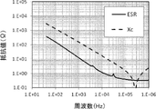
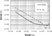
- FIG. 3 is a graph conceptually showing frequency characteristics of the capacitive reactance Xc and the equivalent series resistance ESR of the piezoelectric film 10.
- FIG. 3 A configuration in which a dielectric piezoelectric layer is sandwiched between electrode pairs is represented by an equivalent circuit in which a capacitance, an equivalent series inductance, and an equivalent series resistance are connected in series, similar to a capacitor or the like.
- the equivalent series inductance does not contribute in the audible range (20 Hz to 20 kHz) where the piezoelectric film of the present invention is used, the piezoelectric film 10 has an equivalent It can be expressed as a circuit.
- This capacitive reactance Xc is the ratio of the voltage and the current when driving the piezoelectric layer.
- the equivalent series resistance ESR corresponds to heat generation due to resistance components.
- the equivalent series resistance ESR is caused by the resistance component of the piezoelectric layer, the resistance component of the electrode layer, and the like. It is considered that the heat generated from the piezoelectric layer appears as frictional heat when the piezoelectric particles contained in the piezoelectric layer cause domain motion. In such a piezoelectric layer, as the frequency of the power source increases, the movement of the domain motion does not keep up with the frequency.
- the resistance component of the electrode layer is almost constant regardless of the frequency. Therefore, as shown in FIG. 3, the equivalent series resistance ESR decreases as the frequency increases, and becomes substantially constant after a certain frequency.
- the equivalent series resistance ESR should be reduced.
- the more active the domain motion the higher the piezoelectric performance. That is, a piezoelectric body with high piezoelectric performance tends to generate a large amount of heat. Therefore, it is difficult to suppress heat generation from the piezoelectric layer without sacrificing piezoelectric performance. Therefore, it is difficult to reduce the equivalent series resistance ESR in the low-frequency region where the piezoelectric layer makes a large contribution.
- the contribution of the piezoelectric layer is relatively small, and the contribution of the resistance components such as the electrode layer is large.
- the equivalent series resistance ESR changes depending on the size of the piezoelectric film, etc.
- the capacitive reactance Xc also depends on the size of the piezoelectric film. Therefore, by evaluating the value of the ratio between the equivalent series resistance ESR and the capacitive reactance Xc, it is possible to evaluate the resistance component excluding the influence of the size.
- the value XE1 obtained by dividing the capacitive reactance Xc of the piezoelectric film at a frequency of 1 kHz by the equivalent series resistance ESR is 1
- the value XE20 obtained by dividing Xc at a frequency of 20 kHz by the ESR is 0.6 to 1. .5 range. That is, by setting the value XE 20 at a frequency of 20 kHz to a value close to the value XE 1 at a frequency of 1 kHz, at a frequency of 20 kHz, the ratio of the heat generated energy to the energy used for the piezoelectric effect in the input energy is , a value close to that for a frequency of 1 kHz. Thereby, heat generation can be suppressed while maintaining good piezoelectric characteristics.
- XE 20 is preferably in the range of 0.6 to 1.5, more preferably in the range of 0.8 to 1.3, and in the range of 1.0 to 1.1. is more preferred.
- Methods for suppressing the resistance of the electrode layer include, for example, increasing the thickness of the electrode layer, shortening the path length of current flow, using a material with low volume resistivity as the material of the electrode layer, and improving the film quality of the electrode layer. control, etc. can be considered.
- the resistance of the entire piezoelectric element can be reduced by connecting the plurality of piezoelectric films in parallel.
- XE 20 may be set in the above range by combining a plurality of these methods.
- the electrode layer is too thick, the deformation (vibration) of the piezoelectric layer is hindered and the output (piezoelectric characteristics) is reduced. Therefore, it is preferable to increase the thickness of the electrode layer to such an extent that the piezoelectric characteristics do not deteriorate, but it is difficult to set XE20 within the above range only by adjusting the thickness.
- the length of the path through which the current flows can be adjusted by devising the connection position between the electrode and the wiring from the power supply, but it is difficult to shorten it sufficiently depending on the size of the piezoelectric film. It is difficult to set 20 within the above range. Therefore, it is preferable to set XE 20 in the above range by combining a plurality of the methods described above.
- the piezoelectric layer is a layer made of a polymeric composite piezoelectric body containing piezoelectric particles in a matrix containing a polymeric material, and is a layer that exhibits a piezoelectric effect that expands and contracts when a voltage is applied.
- the piezoelectric layer 20 is composed of a polymeric composite piezoelectric body in which piezoelectric particles 36 are dispersed in a matrix 34 made of a polymeric material having viscoelasticity at room temperature.
- ordinary temperature refers to a temperature range of about 0 to 50.degree.
- the polymer composite piezoelectric body preferably satisfies the following requirements.
- Flexibility For example, when gripping a loosely bent state like a document like a newspaper or magazine for portable use, it is constantly subjected to a relatively slow and large bending deformation of several Hz or less from the outside. become. At this time, if the polymer composite piezoelectric material is hard, a correspondingly large bending stress is generated, and cracks occur at the interface between the polymer matrix and the piezoelectric particles, which may eventually lead to destruction. Therefore, the polymer composite piezoelectric body is required to have appropriate softness. Moreover, stress can be relieved if strain energy can be diffused to the outside as heat. Therefore, it is required that the loss tangent of the polymer composite piezoelectric material is appropriately large.
- the flexible polymer composite piezoelectric material used as an exciter is required to behave hard against vibrations of 20 Hz to 20 kHz and softly against vibrations of several Hz or less.
- the loss tangent of the polymer composite piezoelectric body is required to be moderately large with respect to vibrations of all frequencies of 20 kHz or less.
- the spring constant can be easily adjusted by laminating according to the rigidity (hardness, stiffness, spring constant) of the material to be attached (diaphragm). The thinner it is, the more energy efficient it can be.
- polymer solids have a viscoelastic relaxation mechanism, and as the temperature rises or the frequency decreases, large-scale molecular motion causes a decrease (relaxation) in the storage elastic modulus (Young's modulus) or a maximum loss elastic modulus (absorption). is observed as Among them, the relaxation caused by the micro-Brownian motion of the molecular chains in the amorphous region is called principal dispersion, and a very large relaxation phenomenon is observed.
- the temperature at which this primary dispersion occurs is the glass transition point (Tg), and the viscoelastic relaxation mechanism appears most prominently.
- the polymer composite piezoelectric body (piezoelectric layer 20), by using a polymer material having a glass transition point at room temperature, in other words, a polymer material having viscoelasticity at room temperature as a matrix, it is possible to suppress vibrations of 20 Hz to 20 kHz. This realizes a polymer composite piezoelectric material that is hard at first and behaves softly with respect to slow vibrations of several Hz or less.
- a polymer material having a glass transition point at room temperature ie, 0 to 50° C. at a frequency of 1 Hz, for the matrix of the polymer composite piezoelectric material, because this behavior is favorably expressed.
- the polymer material having viscoelasticity at room temperature Preferably, a polymer material having a maximum value of 0.5 or more in loss tangent Tan ⁇ at a frequency of 1 Hz in a dynamic viscoelasticity test at normal temperature, ie, 0 to 50° C., is used.
- a polymer material having a maximum value of 0.5 or more in loss tangent Tan ⁇ at a frequency of 1 Hz in a dynamic viscoelasticity test at normal temperature, ie, 0 to 50° C. is used.
- the polymer material having viscoelasticity at room temperature preferably has a storage elastic modulus (E') at a frequency of 1 Hz measured by dynamic viscoelasticity of 100 MPa or more at 0°C and 10 MPa or less at 50°C.
- E' storage elastic modulus
- the polymer material having viscoelasticity at room temperature has a dielectric constant of 10 or more at 25°C.
- a voltage is applied to the polymer composite piezoelectric material, a higher electric field is applied to the piezoelectric particles in the polymer matrix, so a large amount of deformation can be expected.
- the polymer material in consideration of ensuring good moisture resistance and the like, it is also suitable for the polymer material to have a dielectric constant of 10 or less at 25°C.
- polymeric materials having viscoelasticity at room temperature examples include cyanoethylated polyvinyl alcohol (cyanoethylated PVA), polyvinyl acetate, polyvinylidene chloride core acrylonitrile, polystyrene-vinylpolyisoprene block copolymer, and polyvinylmethyl.
- cyanoethylated polyvinyl alcohol cyanoethylated PVA
- polyvinyl acetate polyvinylidene chloride core acrylonitrile
- polystyrene-vinylpolyisoprene block copolymer examples include ketones and polybutyl methacrylate.
- Commercially available products such as Hybler 5127 (manufactured by Kuraray Co., Ltd.) can also be suitably used as these polymer materials.
- the polymer material it is preferable to use a material having a cyanoethyl group, and it is particularly preferable to use cyanoethylated PVA. These polymer materials may be used singly or in combination (mixed).
- the matrix 34 using such a polymer material having viscoelasticity at room temperature may use a plurality of polymer materials together, if necessary. That is, in addition to a viscoelastic material such as cyanoethylated PVA, other dielectric polymer materials may be added to the matrix 34 as necessary for the purpose of adjusting dielectric properties and mechanical properties.
- a viscoelastic material such as cyanoethylated PVA
- other dielectric polymer materials may be added to the matrix 34 as necessary for the purpose of adjusting dielectric properties and mechanical properties.
- dielectric polymer materials examples include polyvinylidene fluoride, vinylidene fluoride-tetrafluoroethylene copolymer, vinylidene fluoride-trifluoroethylene copolymer, and polyvinylidene fluoride-trifluoroethylene copolymer.
- fluorine-based polymers such as polyvinylidene fluoride-tetrafluoroethylene copolymer, vinylidene cyanide-vinyl acetate copolymer, cyanoethylcellulose, cyanoethylhydroxysaccharose, cyanoethylhydroxycellulose, cyanoethylhydroxypullulan, cyanoethylmethacrylate, cyanoethylacrylate, cyanoethyl Cyano groups such as hydroxyethylcellulose, cyanoethylamylose, cyanoethylhydroxypropylcellulose, cyanoethyldihydroxypropylcellulose, cyanoethylhydroxypropylamylose, cyanoethylpolyacrylamide, cyanoethylpolyacrylate, cyanoethylpullulan, cyanoethylpolyhydroxymethylene, cyanoethylglycidolpullul
- polymers having cyanoethyl groups and synthetic rubbers such as nitrile rubber and chloroprene rubber are exemplified. Among them, polymer materials having cyanoethyl groups are preferably used. Further, in the matrix 34 of the piezoelectric layer 20, the dielectric polymer added in addition to the material having viscoelasticity at room temperature such as cyanoethylated PVA is not limited to one type, and plural types may be added. .
- the matrix 34 may include thermoplastic resins such as vinyl chloride resin, polyethylene, polystyrene, methacrylic resin, polybutene, and isobutylene, and phenolic resin for the purpose of adjusting the glass transition point Tg. , urea resins, melamine resins, alkyd resins, and thermosetting resins such as mica may be added. Furthermore, a tackifier such as rosin ester, rosin, terpene, terpene phenol, and petroleum resin may be added for the purpose of improving adhesiveness.
- the addition amount is not particularly limited, but the ratio of the material to the matrix 34 is 30% by mass or less. is preferable.
- the characteristics of the polymer material to be added can be expressed without impairing the viscoelastic relaxation mechanism in the matrix 34, so that the dielectric constant can be increased, the heat resistance can be improved, and the adhesion between the piezoelectric particles 36 and the electrode layer can be improved. favorable results can be obtained in terms of
- the piezoelectric particles 36 are made of ceramic particles having a perovskite or wurtzite crystal structure.
- ceramic particles constituting the piezoelectric particles 36 include lead zirconate titanate (PZT), lead zirconate lanthanate titanate (PLZT), barium titanate (BaTiO 3 ), zinc oxide (ZnO), and A solid solution (BFBT) of barium titanate and bismuth ferrite (BiFe 3 ) is exemplified.
- the particle size of the piezoelectric particles 36 is not limited, and may be appropriately selected according to the size of the piezoelectric film 10, the application of the piezoelectric film 10, and the like.
- the particle size of the piezoelectric particles 36 is preferably 1 to 10 ⁇ m. By setting the particle size of the piezoelectric particles 36 within this range, favorable results can be obtained in that the piezoelectric film 10 can achieve both high piezoelectric characteristics and flexibility.
- the piezoelectric particles 36 in the piezoelectric layer 20 are uniformly and regularly dispersed in the matrix 34 in FIG. 2, the present invention is not limited to this. That is, the piezoelectric particles 36 in the piezoelectric layer 20 may be dispersed irregularly in the matrix 34 as long as they are preferably uniformly dispersed.
- the quantitative ratio of the matrix 34 and the piezoelectric particles 36 in the piezoelectric layer 20 is not limited. It may be appropriately set according to the properties required for the piezoelectric film 10 .
- the volume fraction of the piezoelectric particles 36 in the piezoelectric layer 20 is preferably 30% to 80%, more preferably 50% or more, and therefore more preferably 50% to 80%.
- the piezoelectric layer 20 is a polymer composite piezoelectric layer in which piezoelectric particles are dispersed in a viscoelastic matrix containing a polymer material having viscoelasticity at room temperature.
- the present invention is not limited to this, and as the piezoelectric layer, a polymer composite piezoelectric body in which piezoelectric particles are dispersed in a matrix containing a polymer material, which is used in known piezoelectric elements, is used. It is possible.
- the thickness of the piezoelectric layer 20 is not particularly limited, and depends on the application of the piezoelectric film 10, the number of layers of the piezoelectric film 10 in the piezoelectric element described later, the properties required of the piezoelectric film 10, and the like. can be set as appropriate.
- the thickness of the piezoelectric layer 20 is preferably 10 to 300 ⁇ m, more preferably 20 to 200 ⁇ m, even more preferably 30 to 150 ⁇ m.
- the first protective layer 28 and the second protective layer 30 cover the second electrode layer 26 and the first electrode layer 24, and provide the piezoelectric layer 20 with appropriate rigidity and mechanical strength. is responsible for That is, in the piezoelectric film 10, the piezoelectric layer 20 made up of the matrix 34 and the piezoelectric particles 36 exhibits excellent flexibility against slow bending deformation, but depending on the application, the rigidity may increase. and mechanical strength may be insufficient.
- the piezoelectric film 10 is provided with a first protective layer 28 and a second protective layer 30 to compensate.
- Various sheet materials can be used for the first protective layer 28 and the second protective layer 30 without limitation, and various resin films are preferably exemplified as examples.
- various resin films are preferably exemplified as examples.
- PET polyethylene terephthalate
- PP polypropylene
- PS polystyrene
- PC polycarbonate
- PPS polyphenylene sulfite
- PMMA polymethyl methacrylate
- PET polyethylene terephthalate
- PET polypropylene
- PS polystyrene
- PC polycarbonate
- PPS polyphenylene sulfite
- PMMA polymethyl methacrylate
- PET polyethylene terephthalate
- PEI polyetherimide
- PI polyimide
- PEN polyethylene naphthalate
- TAC triacetyl cellulose
- cyclic olefin resins and the like are preferably used.
- the thicknesses of the first protective layer 28 and the second protective layer 30 are also not limited. Also, the thicknesses of the first protective layer 28 and the second protective layer 30 are basically the same, but may be different. Here, if the rigidity of the first protective layer 28 and the second protective layer 30 is too high, not only will the expansion and contraction of the piezoelectric layer 20 be restricted, but also the flexibility will be impaired. Therefore, the thinner the first protective layer 28 and the second protective layer 30, the better, except for cases where mechanical strength and good handling properties as a sheet-like article are required.
- the thickness of the first protective layer 28 and the second protective layer 30 is not more than twice the thickness of the piezoelectric layer 20, it is possible to ensure both rigidity and appropriate flexibility. favorable results can be obtained.
- the thickness of the piezoelectric layer 20 is 50 ⁇ m and the first protective layer 28 and the second protective layer 30 are made of PET, the thicknesses of the first protective layer 28 and the second protective layer 30 are preferably 100 ⁇ m or less. 50 ⁇ m or less is more preferable, and 25 ⁇ m or less is even more preferable.
- a first electrode layer 24 is provided between the piezoelectric layer 20 and the first protective layer 28, and a second electrode layer 26 is provided between the piezoelectric layer 20 and the second protective layer 30. It is formed. The first electrode layer 24 and the second electrode layer 26 are provided for applying voltage to the piezoelectric layer 20 (piezoelectric film 10).
- the materials for forming the first electrode layer 24 and the second electrode layer 26 are not limited, and various conductors can be used. Specifically, metals such as carbon, palladium, iron, tin, aluminum, nickel, platinum, gold, silver, copper, titanium, chromium and molybdenum, alloys thereof, laminates and composites of these metals and alloys, Also, indium tin oxide and the like are exemplified. Among them, copper, aluminum, gold, silver, platinum, and indium tin oxide are used for the first electrode layer 24 and the second electrode layer 26 from the viewpoint that it is easy to adjust the XE 20 to the above range. It is exemplified favorably as a material.
- the method of forming the first electrode layer 24 and the second electrode layer 26 is not limited, and vapor phase deposition methods (vacuum film formation methods) such as vacuum deposition, ion-assisted deposition, and sputtering, film formation by plating, Alternatively, various known methods such as a method of adhering a foil made of the above material can be used.
- vapor phase deposition methods vacuum film formation methods
- ion-assisted deposition ion-assisted deposition
- sputtering film formation by plating
- various known methods such as a method of adhering a foil made of the above material can be used.
- the resistance changes depending on the film quality of the electrode layer (metal film). For example, if there are many crystal grain boundaries and voids in the film, the resistance will increase. Therefore, it is preferable to adjust the film quality of the electrode layer by controlling the formation method and formation conditions of the electrode layer.
- Ion-assisted vapor deposition and sputtering are preferable as the formation method for reasons such as the ability to form a low-resistance film with good film quality.
- Metal thin films grown by vapor-phase deposition methods such as sputtering and vapor deposition generally have a columnar structure.
- a columnar structure consisting of grains is ideal.
- the substrate temperature is raised as much as possible to promote surface diffusion, while the gas pressure is lowered as much as possible to lengthen the mean free path and suppress the projection effect.
- a columnar structure with a large diameter can be obtained.
- it is also effective to accelerate the surface diffusion by bombarding the substrate with high-speed charged particles such as ion assist.
- the thicknesses of the first electrode layer 24 and the second electrode layer 26 are not limited. Also, the thicknesses of the first electrode layer 24 and the second electrode layer 26 are basically the same, but may be different.
- the rigidity of the first electrode layer 24 and the second electrode layer 26 is too high, not only will the expansion and contraction of the piezoelectric layer 20 be restricted, Flexibility is also impaired. Therefore, from the viewpoint of flexibility and piezoelectric properties, the thinner the first electrode layer 24 and the second electrode layer 26 are, the better. On the other hand, if the first electrode layer 24 and the second electrode layer 26 are too thin, the electrical resistance will be high and it will be difficult to satisfy the range of XE 20 mentioned above.
- the thickness of the first electrode layer 24 and the second electrode layer 26 is preferably 3 ⁇ m or less, more preferably 2 ⁇ m or less, and even more preferably 1 ⁇ m or less.
- the thickness of the first electrode layer 24 and the second electrode layer 26 is preferably 0.1 ⁇ m or more, more preferably 0.2 ⁇ m or more, and even more preferably 0.3 ⁇ m or more.
- Wiring from a power supply is connected to the first electrode layer 24 and the second electrode layer 26.
- the connecting portion between the first electrode layer 24 and the wiring and the connecting portion between the second electrode layer 26 and the wiring on the long side it is preferable to connect each electrode layer and the wiring at a plurality of points.
- the piezoelectric film 10 preferably includes the piezoelectric layer 20 formed by dispersing the piezoelectric particles 36 in the matrix 34 containing a polymer material having viscoelasticity at room temperature, the first electrode layer 24 and the second electrode layer 24 . It is sandwiched between the electrode layers 26, and further has a configuration in which this laminate is sandwiched between the first protective layer 28 and the second protective layer 30.
- the maximum value of the loss tangent (Tan ⁇ ) at a frequency of 1 Hz by dynamic viscoelasticity measurement preferably exists at room temperature, and the maximum value of 0.1 or more exists at room temperature. more preferred.
- the piezoelectric film 10 preferably has a storage elastic modulus (E') at a frequency of 1 Hz measured by dynamic viscoelasticity measurement of 10 to 30 GPa at 0°C and 1 to 10 GPa at 50°C. Accordingly, the piezoelectric film 10 can have a large frequency dispersion in the storage elastic modulus (E') at room temperature. That is, it can act hard against vibrations of 20 Hz to 20 kHz and soft against vibrations of several Hz or less.
- E' storage elastic modulus
- the piezoelectric film 10 has a product of thickness and storage elastic modulus (E′) at a frequency of 1 Hz measured by dynamic viscoelasticity measurement of 1.0 ⁇ 10 6 to 2.0 ⁇ 10 6 N/m at 0° C. , 1.0 ⁇ 10 5 to 1.0 ⁇ 10 6 N/m at 50°C.
- E′ thickness and storage elastic modulus
- the piezoelectric film 10 preferably has a loss tangent (Tan ⁇ ) of 0.05 or more at 25° C. and a frequency of 1 kHz in a master curve obtained from dynamic viscoelasticity measurement.
- Ton ⁇ loss tangent
- the frequency characteristics of the speaker using the piezoelectric film 10 are smoothed, and the amount of change in sound quality when the lowest resonance frequency f0 changes as the curvature of the speaker changes can be reduced.
- FIG. 1 An example of a method for manufacturing the piezoelectric film 10 will be described below with reference to FIGS. 4 to 6.
- FIG. 1 An example of a method for manufacturing the piezoelectric film 10 will be described below with reference to FIGS. 4 to 6.
- a sheet-like object 10a having a first electrode layer 24 formed on a first protective layer 28 is prepared.
- This sheet-like object 10a may be produced by forming a copper thin film or the like as the first electrode layer 24 on the surface of the first protective layer 28 by vacuum deposition, sputtering, plating, or the like.
- the first protective layer 28 with a separator temporary support
- PET or the like having a thickness of 25 ⁇ m to 100 ⁇ m can be used.
- the separator may be removed after the second electrode layer 26 and the second protective layer 30 are thermally compressed and before laminating any member on the first protective layer 28 .
- a coating material is prepared by dissolving a polymer material as a matrix material in an organic solvent, adding piezoelectric particles 36 such as PZT particles, and stirring and dispersing the mixture.
- Organic solvents other than the above substances are not limited and various organic solvents can be used.
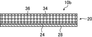
- the paint is cast (applied) on the sheet-like material 10a and dried by evaporating the organic solvent.
- the laminate 10b having the first electrode layer 24 on the first protective layer 28 and the piezoelectric layer 20 on the first electrode layer 24 is produced.
- the first electrode layer 24 refers to the electrode on the substrate side when the piezoelectric layer 20 is applied, and does not indicate the vertical positional relationship in the laminate.
- the matrix 34 may be added with a dielectric polymer material other than a viscoelastic material such as cyanoethylated PVA.
- a dielectric polymer material other than a viscoelastic material such as cyanoethylated PVA.
- the polarization of the piezoelectric layer 20 is preferably Perform processing (polling).
- the method of polarization treatment of the piezoelectric layer 20 is not limited, and known methods can be used.
- the surface of the piezoelectric layer 20 may be smoothed by using a heating roller or the like, which is a calendering treatment. By performing this calendering process, the thermocompression bonding process, which will be described later, can be performed smoothly.
- the sheet-like object 10c is prepared in which the second electrode layer 26 is formed on the second protective layer 30.
- FIG. This sheet-like object 10c may be produced by forming a copper thin film or the like as the second electrode layer 26 on the surface of the second protective layer 30 by vacuum deposition, sputtering, plating, or the like.
- the second electrode layer 26 is directed toward the piezoelectric layer 20, and the sheet-like object 10c is laminated on the laminate 10b for which the polarization treatment of the piezoelectric layer 20 has been completed.
- the laminate of the laminate 10b and the sheet material 10c is thermocompression bonded with a heat press device, a pair of heating rollers, etc., with the second protective layer 30 and the first protective layer 28 sandwiched therebetween, and then, as desired.
- the piezoelectric film 10 is produced by cutting into the shape of .
- the processes up to this point can also be carried out while transporting a sheet that is not in the form of a sheet, but in the form of a web, that is, a sheet wound up in a long continuous state.
- Both the laminate 10b and the sheet-like material 10c can be web-like and can be thermocompressed as described above. In that case, the piezoelectric film 10 is produced in web form at this point.
- a special glue layer may be provided when laminating the laminate 10b and the sheet-like material 10c.
- a glue layer may be provided on the surface of the second electrode layer 26 of the sheet 10c.
- the most preferred glue layer is the same material as matrix 34 . It is also possible to apply the same material to the surface of the second electrode layer 26 and bond them together.
- the laminated piezoelectric element 50 has a configuration in which a plurality of piezoelectric films 10 are laminated (hereinafter also referred to as a single-wafer type laminated piezoelectric element). is not limited to this and various configurations are available.
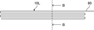
- the laminated piezoelectric element 56 shown in FIG. 7 uses a plurality of the same members as the laminated piezoelectric element 50 described above.
- a laminated piezoelectric element 56 shown in FIG. 7 is obtained by laminating a plurality of piezoelectric films in layers by folding a long piezoelectric film 10L in the longitudinal direction one or more times, preferably a plurality of times.
- the piezoelectric element 56 shown in FIG. By folding and stacking one long piezoelectric film 10L polarized in the thickness direction, the polarization direction of the piezoelectric film adjacent (facing) in the stacking direction is as indicated by the arrow in FIG. , in the opposite direction.
- FIG. 7 omits illustration of the first protective layer 28 and the second protective layer 30 of the piezoelectric film 10L, the piezoelectric film 10L has the first protective layer 28 and the second protective layer 30.
- the laminated piezoelectric element 56 can be configured with only one long piezoelectric film 10L, only one power source PS is required for applying the drive voltage, and the electrodes from the piezoelectric film 10L can be connected. drawer is also good in one place. Therefore, according to the laminated piezoelectric element 56 shown in FIG. 7, the number of parts can be reduced, the configuration can be simplified, the reliability of the piezoelectric element (module) can be improved, and the cost can be reduced. .
- a bellows type piezoelectric element such a structure in which one sheet of long piezoelectric film 10L is folded back (hereinafter also referred to as a bellows type piezoelectric element) tends to have a long path through which current flows. Since a plurality of piezoelectric films cannot be connected in parallel as described above, a single-wafer laminated piezoelectric element is preferable from the viewpoint of satisfying the range of XE 20 described above.
- the piezoelectric element 56 shown in FIG. 7 in the piezoelectric element 56 obtained by folding the long piezoelectric film 10L, it is preferable to insert the core rod 58 into the folded portion of the piezoelectric film 10L while contacting the piezoelectric film 10L.
- the first electrode layer 24 and the second electrode layer 26 of the piezoelectric film 10L are formed of metal deposition films or the like. If the vapor-deposited metal film is bent at an acute angle, cracks or the like are likely to occur, which may lead to disconnection of the electrode. That is, in the piezoelectric element 56 shown in FIG. 7, cracks or the like easily occur in the electrodes inside the bent portion.
- the first electrode layer 24 and the second electrode layer 26 are folded by inserting the core rod 58 into the folded portion of the piezoelectric film 10L. can be prevented, and the occurrence of disconnection can be suitably prevented.
- Adhesive layer 19 for adhering piezoelectric films 10 together and adhesive layer 16 for adhering laminated piezoelectric element 50 and diaphragm 12 are not limited, and various known adhesives and adhesives can be used. be.
- Various known adhesive layers can be used as long as the members can be adhered to each other. Therefore, the adhesive layer has fluidity at the time of bonding and then becomes a solid. Even a layer made of an adhesive is a gel-like (rubber-like) soft solid at the time of bonding and remains gel-like after that. It may be a layer made of an adhesive whose state does not change, or a layer made of a material having the characteristics of both an adhesive and an adhesive.
- the vibration plate 12 is vibrated to generate sound. Therefore, it is preferable that the expansion and contraction of each piezoelectric film 10 is directly transmitted. If a substance having a viscosity that reduces vibration is present between the piezoelectric films 10, the efficiency of transmission of the energy of expansion and contraction of the piezoelectric films 10 will be lowered, and the driving efficiency of the piezoelectric films 10 will be lowered.
- the adhesive layer is preferably an adhesive layer made of an adhesive, which provides a solid and hard adhesive layer, rather than an adhesive layer made of an adhesive.
- More preferable adhesive layers are specifically exemplified by adhesive layers made of thermoplastic adhesives such as polyester adhesives and styrene-butadiene rubber (SBR) adhesives. Adhesion, unlike sticking, is useful in seeking high adhesion temperatures. Further, a thermoplastic type adhesive is suitable because it has "relatively low temperature, short time, and strong adhesion".
- the thickness of the adhesive layer is not limited, and the thickness that can exhibit sufficient sticking force (adhesive force, cohesive force) may be appropriately set according to the material forming the adhesive layer.
- adheresive force cohesive force
- the thinner the adhesive layer is the higher the effect of transmitting the expansion/contraction energy (vibration energy) of the piezoelectric layer 20 can be and the higher the energy efficiency can be.
- the adhesive layer is thick and rigid, it may restrict expansion and contraction of the piezoelectric film.
- the adhesive layer is preferably thinner than the piezoelectric layer 20 .
- the adhesive layer is preferably hard and thin.
- the thickness of the adhesive layer after sticking is preferably 0.1 to 50 ⁇ m, more preferably 0.1 to 30 ⁇ m, even more preferably 0.1 to 10 ⁇ m.
- the spring constant of the adhesive layer is high, the expansion and contraction of the piezoelectric film 10 may be restricted. Therefore, it is preferable that the spring constant of the adhesive layer is equal to or less than the spring constant of the piezoelectric film 10 .
- the spring constant is "thickness x Young's modulus".
- the product of the thickness of the adhesive layer and the storage elastic modulus (E′) at a frequency of 1 Hz by dynamic viscoelasticity measurement is 2.0 ⁇ 10 6 N / m or less at 0 ° C. and at 50 ° C. It is preferably 1.0 ⁇ 10 6 N/m or less.
- the internal loss at a frequency of 1 Hz by dynamic viscoelasticity measurement of the adhesive layer is 1.0 or less at 25 ° C. for the adhesive layer, and at 25 ° C. for the adhesive layer. It is preferably 0.1 or less.
- ⁇ Diaphragm> Various articles can be used as the diaphragm 12 without limitation.
- the diaphragm 12 include plate materials such as resin plates and glass plates, advertising notice media such as signboards, office equipment and furniture such as tables, whiteboards and projection screens, organic electroluminescence (OLED) Light Emitting Diode)) Display devices such as displays and liquid crystal displays, vehicle components such as consoles, A-pillars, ceilings and bumpers such as automobiles, and building materials such as walls of houses.
- plate materials such as resin plates and glass plates
- advertising notice media such as signboards, office equipment and furniture such as tables, whiteboards and projection screens, organic electroluminescence (OLED) Light Emitting Diode)
- Display devices such as displays and liquid crystal displays, vehicle components such as consoles, A-pillars, ceilings and bumpers such as automobiles, and building materials such as walls of houses.
- the diaphragm 12 to which the laminated piezoelectric element 50 of the present invention is attached preferably has flexibility, and more preferably can be wound up.
- a panel-shaped display device having flexibility such as a flexible display panel is particularly preferably exemplified.
- the display device is also rollable.
- the laminated piezoelectric element 50 is also adjusted according to the winding curvature of the diaphragm 12. Preferably, it bends with 12 .
- the laminated piezoelectric element 50 of the present invention also basically exhibits good flexibility.
- the winding curvature of the diaphragm 12 is basically a specific curvature, but the winding curvature of the diaphragm 12 may be variable.
- the laminated piezoelectric element 50 is preferably attached to the back side of the display device, that is, to the non-image display side of the display device.
- the size of the adhesive layer 16 in the planar direction is preferably equal to or smaller than the planar size of the laminated piezoelectric element 50 .
- the display device itself such as a flexible display panel may be used as the diaphragm 12, or a plate-like member provided in the display device or a plate engaged with the display device may be used.
- the diaphragm 12 may be a shaped member.
- the driving current is applied to the piezoelectric film 10 while the diaphragm 12 is not wound. I prefer not to.
- a drive current is applied to the piezoelectric film 10 and/or the diaphragm 12 in a state where the diaphragm 12 is not wound, and the diaphragm
- the piezoelectric film 10 and/or the diaphragm 12 are not energized when the film 12 is wound.
- Various known methods can be used as the method for switching between energization and non-energization.
- the planar shape of the laminated piezoelectric element is preferably rectangular (rectangular) (see FIG. 15).
- the length of the long side W2 is increased without changing the length W1 of the short side , thereby increasing the sound pressure with the same applied voltage. can be higher. Therefore, the voltage for obtaining the same sound pressure can be made lower, and the amount of heat generated can be suppressed.
- FIG. 15 shows a plan view of an example of a rectangular laminated piezoelectric element.
- FIG. 16 shows a side view of FIG. 15 viewed from the short side. In FIG. 16, illustration of the adhesive layer and the lead-out portion of the electrode is omitted.
- the example shown in FIGS. 15 and 16 is an example in which a long piezoelectric film 10L is folded several times to form a laminate. In the examples shown in FIGS. 15 and 16, the direction of multiple folds is the direction of the short side.
- the regions to be folded and laminated are folded so that the short sides have the same length. It is formed to have an overhang 60 . As shown in FIG. 15, electrode lead portions (62, 64) are provided near both ends of the overhang portion 60 in the long side direction.
- the planar shape of the laminated piezoelectric element is rectangular, and the length W2 of the long side is increased without changing the length W1 of the short side , thereby suppressing the amount of heat generated. It may be combined with the laminated piezoelectric element of the invention.
- the ratio of the length W 2 of the long side to the length W 1 of the short side is preferably 3 to 30, more preferably 3 to 20, and 3 to 3. 10 is more preferred.
- a laminated body of piezoelectric films having longer long sides is prepared in advance, and then the necessary By cutting according to the thickness, the manufacturing process can be further simplified.
- a piezoelectric film laminate having a long side of 46 cm ⁇ a short side of 3 cm is prepared and cut at a position of 20 cm from one of the short sides to obtain a laminated piezoelectric element of a long side of 20 cm ⁇ a short side of 3 cm and a long side of the piezoelectric film.
- a laminated piezoelectric element of 26 cm ⁇ 3 cm short side can be produced.
- FIG. 17 shows an enlarged view of a part of the BB line cross section when the long piezoelectric film 10L is folded several times to form a laminated body and cut parallel to the paper surface. .
- the ends of the short sides of each layer of the piezoelectric film 10L are deformed in the same direction.
- the ends of each layer are deformed downward. Since the cut ends of the layers deform in the same direction in this way, it is possible to prevent the electrode layers between the layers from coming into contact with each other and causing a short circuit.
- the adhesive layer 19 is provided between each layer, the adhesive layer serves as an insulator, and it is possible to prevent the electrode layers between the layers from coming into contact with each other and causing a short circuit.
- the cut piezoelectric film 10L may be folded several times and laminated. In this case, as shown in FIG. 18, the ends of the short sides of each layer of the piezoelectric film 10L are deformed in the opposite direction to the adjacent layers.
- the piezoelectric film 10L is folded and laminated multiple times, since the electrode layers facing each other are connected to each other, there is no problem even if they come into contact with each other. Short circuits can be prevented.
- the method of connecting the electrode layer of the piezoelectric film and the wiring is not particularly limited, and various known methods can be used for connection.
- the electrode layer and the protective layer may protrude outwardly from the piezoelectric layer in the plane direction, and the wiring may be connected to the electrode layer of the projecting portion.
- a part of the protective layer (the second protective layer 30 in FIG. 20) is removed to form a hole 70, and silver paste or the like is applied to the hole 70.
- the conductive member 72 is arranged to electrically connect the conductive member 72 and the electrode layer (second electrode layer 26 in FIG. 20), and the electrode layer (second electrode layer 26) is electrically connected through the conductive member 72. You may connect wiring (conductor 74a) to .
- a protective layer is arranged at least on the electrode layer on the outermost layer side of the piezoelectric film arranged on the outermost layer of the laminated piezoelectric element. Note that all the piezoelectric films of the sheet-type laminated piezoelectric element may have a protective layer.
- the protective layer has a hole penetrating from the surface to the electrode layer, a conductive member is arranged (filled) in the hole, and a conductive wire (wiring) is electrically connected to the electrode layer through the conductive member, if A is the opening area of the hole, t is the thickness of the electrode layer, and C is the capacitance of the laminated piezoelectric element, then C/ (Axt) is preferably 260 ⁇ F/mm 3 or less.
- C/(Axt) is more preferably 260 ⁇ F/mm 3 or less, and even more preferably 150 ⁇ F/mm 3 or less.
- C / (A ⁇ t) is preferably 50 ⁇ F / mm 3 or more
- the electrostatic capacitance C of the laminated piezoelectric element is measured between the wiring drawn from each electrode layer of the piezoelectric film constituting the laminated piezoelectric element using an LCR meter (for example, ZM2372 manufactured by NF Circuit Design Block Co., Ltd.). and measure it. The measurement was performed at a measurement frequency of 1 kHz and a voltage of 5V.
- LCR meter for example, ZM2372 manufactured by NF Circuit Design Block Co., Ltd.
- the capacitance C of the piezoelectric film is determined according to the thickness of the piezoelectric layer, the area of the piezoelectric layer, and the dielectric constant of the piezoelectric layer. Therefore, by adjusting these, the capacitance C of the piezoelectric film can be adjusted.
- the opening area A (area in plan view) of the hole can be measured by removing the conducting wire and exposing the hole of the protective layer with a CNC image measuring machine (such as Quick Vision manufactured by Mitutoyo Co., Ltd.). can. If the contour of the hole is not visible, the conductive member may be removed. At this time, it is necessary to select a method that does not damage the protective layer.
- a CNC image measuring machine such as Quick Vision manufactured by Mitutoyo Co., Ltd.
- the opening area A of the hole is large. On the other hand, if the opening area A of the hole is too large, it is disadvantageous in terms of productivity.
- the shape of the opening of the hole (the shape in plan view) is not limited, and may be various shapes such as circular, elliptical, rectangular, polygonal, and irregular. A circular shape is preferable from the viewpoint of ease of formation.
- the method for forming the holes is not limited, and a known method may be used depending on the material for forming the protective layer. Examples of the method for forming the hole include laser processing, removal by dissolution using a solvent, and mechanical processing such as mechanical polishing.
- the thickness of the electrode layer can be measured by cutting the piezoelectric film using an ultramicrotome (UC6 manufactured by Leica, etc.) and then observing the cross section using an SEM (SU8220 manufactured by Hitachi High-Tech, etc.).
- U6 ultramicrotome
- SEM SEM
- conductive paste such as silver paste, solder, conductive cloth, metal cloth, conductive urethane foam, and the like can be used.
- a material containing silver, copper, gold, carbon, nickel, solder, or the like as a filler is used.
- the conductive paste may be filled into the holes using a dispenser or the like.
- the conductive paste is preferably filled in a sufficient amount so as to fill the holes. More preferably, the conductive paste is filled in an amount that rises from the hole, or the conductive paste is filled in an amount that overflows the hole.
- a conductive cloth is, for example, a woven or non-woven fabric woven from resin threads coated with a metal film by plating or the like.
- Various known conductive cloths can be used as the conductive cloth.
- the conductive cloth a conductive cloth obtained by plating the surface of a thread made of PET with Cu or Ni is exemplified.
- Sui-10-511M manufactured by Seiren Co., Ltd. can be used as the conductive cloth.
- a metal cloth is a woven or non-woven fabric woven with metal threads.
- Various known metal cloths can be used as the metal cloth.
- a plain weave wire mesh ⁇ 0.05 ⁇ 200 m/s manufactured by Okutani Wire Net Mfg. Co., Ltd. can be used as the metal cloth.
- Conductive urethane foam is made by supporting conductive particles such as carbon black on soft urethane foam.
- Various known conductive urethane foams can be used as the conductive urethane foam.
- the thickness of the conductive member is preferably greater than the thickness of the protective layer. Thereby, the conductive member and the conducting wire can be reliably connected.
- a sheet-like object (metal foil) or a wire-like object (metal wire) made of a conductive metal material can be used as the conducting wire. Copper, aluminum, nickel, tin, gold, silver and the like are preferably exemplified as the material of the conductor wire. Moreover, you may use an FFC cable as a conductor.
- the conductive wire may have any shape and size as long as it can be electrically connected to the conductive member and can be used as an extraction electrode.
- connection between the conducting wire and the conductive member may be performed by a known method.
- the conductive member is a conductive paste
- the conductive wire and the conductive member may be connected by curing the conductive paste after bringing the conductive wire and the conductive paste into contact with each other.
- the conducting wire and the conducting member may be connected by covering at least a portion of the contact portion and adhering an adhesive tape onto the protective layer while the conducting wire and the conducting member are in contact with each other.
- the connection between the conducting wire and the conducting member may be fixed by adhering the conducting wire and the protective layer while the conducting wire and the conducting member are in contact with each other.
- the laminated piezoelectric element of the present invention has been described in detail above, the present invention is not limited to the above examples, and various improvements and changes may be made without departing from the gist of the present invention. Of course.
- Sheets 10a and 10c were prepared by forming a copper thin film with a thickness of 100 nm on a PET film with a thickness of 4 ⁇ m by sputtering. That is, in this example, the first electrode layer 24 and the second electrode layer 26 are copper thin films with a thickness of 100 nm, and the first protective layer 28 and the second protective layer 30 are PET films with a thickness of 4 ⁇ m.
- the gas pressure for sputtering the copper thin film onto the PET film was 0.4 Pa, and the substrate temperature (the temperature of the PET film) was 120°C.
- sputtering 1 In the column of the electrode layer forming method in Table 1 below, the case where sputtering is performed under the same conditions as in Example 1 is referred to as "sputtering 1".
- a PET film with a separator temporary support PET having a thickness of 50 ⁇ m was used, and the separator of each protective layer was removed after the sheet-like material 10c was thermocompressed. rice field.
- cyanoethylated PVA (CR-V, manufactured by Shin-Etsu Chemical Co., Ltd.) was dissolved in methyl ethyl ketone (MEK) at the following composition ratio.
- PZT particles were added to this solution in the following composition ratio and dispersed with a propeller mixer (rotation speed: 2000 rpm) to prepare a paint for forming the piezoelectric layer 20 .
- ⁇ PZT particles ⁇ 300 parts by mass
- ⁇ Cyanoethylated PVA ⁇ 15 parts by mass ⁇ MEK ⁇ 85 parts by mass
- the PZT particles used were obtained by sintering a commercially available PZT raw material powder at 1000 to 1200° C. and then pulverizing and classifying the sintered particles to an average particle size of 5 ⁇ m.
- the previously prepared paint for forming the piezoelectric layer 20 was applied onto the first electrode layer 24 (copper thin film) of the sheet 10a previously prepared.
- the paint was applied so that the thickness of the coating film after drying was 20 ⁇ m.
- the sheet material 10a coated with the paint was dried by heating on a hot plate at 120° C. to evaporate the MEK, thereby forming the laminate 10b.
- a sheet 10c was laminated on the laminated body 10b with the second electrode layer 26 (copper thin film side) side facing the piezoelectric layer 20, and was thermocompression bonded at 120.degree.
- the piezoelectric film 10 having the first protective layer 28, the first electrode layer 24, the piezoelectric layer 20, the second electrode layer 26 and the second protective layer 30 in this order was produced.
- the produced piezoelectric film was cut into a size of 200 mm ⁇ 190 mm in plan view and folded four times in the longitudinal direction to produce a bellows-shaped piezoelectric element 56 .
- the surfaces to be folded back and in contact with each other were bonded together using a thermal adhesive sheet (FB-ML4 manufactured by Nitto Shinko Co., Ltd.).
- FB-ML4 thermal adhesive sheet manufactured by Nitto Shinko Co., Ltd.
- the first electrode layer 24 and wiring were connected at one end of the long side of the folded piezoelectric film as described below, and the second electrode layer 26 and wiring were connected at the other end.
- a hole was formed in each of the first protective layer and the second protective layer using a laser processing machine.
- the opening shape of the hole was circular, and the opening area was 60 mm 2 .
- a conductive paste containing a Ni filler was used as the conductive member, and a copper foil having a thickness of 35 ⁇ m was used as the wiring (conductive wire). After filling the holes with the conductive paste using a dispenser, the wiring was brought into contact with the hole and the conductive paste was dried and cured.
- the capacitance between the wiring connected to the first electrode layer 24 and the wiring connected to the second electrode layer 26 of the manufactured laminated piezoelectric element is measured by an LCR meter (for example, NF Circuit Design Block Co., Ltd.). When measured using ZM2372), it was 1.2 ⁇ F. Therefore, C/(A ⁇ t) obtained by dividing the capacitance C by the opening area A of the hole and the thickness t of the electrode layer was 200.0 ⁇ F/mm 3 .
- Example 2 A piezoelectric film was produced in the same manner as in Example 1, except that the thickness of the first electrode layer 24 and the second electrode layer 26 (copper thin film) was 150 nm.
- Example 3 Five piezoelectric films 10 having a size of 200 mm ⁇ 38 mm in plan view were cut from the piezoelectric film 10 produced in Example 1, and the five piezoelectric films 10 cut out were laminated to produce a single-wafer type piezoelectric element 50 . Adjacent piezoelectric films 10 were bonded together using a thermal adhesive sheet (FB-ML4 manufactured by Nitto Shinko Co., Ltd.). Also, the first electrode layer 24 and the wiring were connected on one side in the width direction of each 200 mm side of each piezoelectric film 10, and the second electrode layer 26 and the wiring were connected on the other side. That is, the first electrode layer 24 and the wiring of each piezoelectric film 10, and the second electrode layer 26 and the wiring were connected at two points. Moreover, each piezoelectric film 10 was connected in parallel.
- FB-ML4 thermal adhesive sheet
- the electrostatic capacity of the produced laminated piezoelectric element was 1.2 ⁇ F.
- C/(Axt) was 200.0 ⁇ F/mm 3 .
- Example 4 A sheet-type piezoelectric element 50 was fabricated in the same manner as in Example 3, except that a copper thin film was formed by ion-assisted vapor deposition and the thickness was set to 150 nm.
- ST55 (1500 W, 7 A, 225 eV) manufactured by TELEMARK was used as an ion gun for ion-assisted vapor deposition of a copper thin film on a PET film.
- Example 5 A bellows-type piezoelectric element was produced in the same manner as in Example 2, except that the opening area A of the hole was 40 mm 2 .
- the capacitive reactance Xc and equivalent series resistance ESR of the manufactured piezoelectric element were measured by the methods described above.
- the capacitive reactance Xc at 20 kHz was 8.36 ⁇ , and the equivalent series resistance ESR was 0.68 ⁇ . Therefore, the ratio Xc/ESR between the capacitive reactance Xc and the equivalent series resistance ESR was 12.3.
- Xc/ESR at 20 kHz when Xc/ESR at 1 kHz is 1, that is, XE 20 was 1.08.
- the electrostatic capacity of the produced laminated piezoelectric element was 1.2 ⁇ F.
- C/(Axt) was 200.0 ⁇ F/mm 3 .
- Example 6 A piezoelectric film was produced in the same manner as in Example 1 except that the thickness of the first electrode layer 24 and the second electrode layer 26 (copper thin film) was 300 nm and the opening area A of the hole was 20 mm 2 .
- the capacitive reactance Xc and equivalent series resistance ESR of the manufactured piezoelectric element were measured by the methods described above.
- the capacitive reactance Xc at 20 kHz was 8.44 ⁇ , and the equivalent series resistance ESR was 0.49 ⁇ . Therefore, the ratio Xc/ESR between the capacitive reactance Xc and the equivalent series resistance ESR was 17.2.
- Xc/ESR at 20 kHz when Xc/ESR at 1 kHz is 1, that is, XE 20 was 1.21.
- the electrostatic capacity of the produced laminated piezoelectric element was 1.2 ⁇ F.
- C/(Axt) was 200.0 ⁇ F/mm 3 .
- Example 7 A piezoelectric film was produced in the same manner as in Example 6, except that the opening area A of the holes was 30 mm 2 .
- the capacitive reactance Xc and equivalent series resistance ESR of the manufactured piezoelectric element were measured by the methods described above.
- the capacitive reactance Xc at 20 kHz was 8.43 ⁇ , and the equivalent series resistance ESR was 0.44 ⁇ . Therefore, the ratio Xc/ESR between the capacitive reactance Xc and the equivalent series resistance ESR was 19.2.
- Xc/ESR at 20 kHz when Xc/ESR at 1 kHz is 1, that is, XE 20 was 1.33.
- Example 8 A piezoelectric film was produced in the same manner as in Example 6, except that the opening area A of the hole was 15 mm 2 .
- the capacitive reactance Xc and equivalent series resistance ESR of the manufactured piezoelectric element were measured by the methods described above.
- the capacitive reactance Xc at 20 kHz was 8.46 ⁇ , and the equivalent series resistance ESR was 0.54 ⁇ . Therefore, the ratio Xc/ESR between the capacitive reactance Xc and the equivalent series resistance ESR was 15.7.
- Xc/ESR at 20 kHz when Xc/ESR at 1 kHz is 1, that is, XE 20 was 1.12.
- Example 1 A bellows-type piezoelectric element was fabricated in the same manner as in Example 1, except that the copper thin film was formed by vacuum deposition. A resistance heating system was used as the vapor deposition source for vacuum vapor deposition of the copper thin film on the PET film, the substrate temperature was 50° C., and the gas pressure was 5 ⁇ 10 ⁇ 3 Pa.
- the electrostatic capacity of the produced laminated piezoelectric element was 1.2 ⁇ F.
- C/(Axt) was 200.0 ⁇ F/mm 3 .
- the electrostatic capacity of the produced laminated piezoelectric element was 1.2 ⁇ F.
- C/(Axt) was 200.0 ⁇ F/mm 3 .
- Example 3 The piezoelectric film produced in Example 1 was cut into a size of 200 mm ⁇ 380 mm in plan view, and folded nine times in the longitudinal direction to produce a bellows-shaped piezoelectric element 56 .
- the surfaces to be folded back and in contact with each other were bonded together using a thermal adhesive sheet (FB-ML4 manufactured by Nitto Shinko Co., Ltd.).
- FB-ML4 thermal adhesive sheet manufactured by Nitto Shinko Co., Ltd.
- the first electrode layer 24 and the wiring were connected at one end of the long side of the folded piezoelectric film, and the second electrode layer 26 and the wiring were connected at the other end.
- the electrostatic capacity of the produced laminated piezoelectric element was 2.4 ⁇ F.
- C/(Axt) was 400.0 ⁇ F/mm 3 .
- the capacitive reactance Xc and equivalent series resistance ESR of the manufactured piezoelectric element were measured by the methods described above.
- the capacitive reactance Xc at 20 kHz was 8.31 ⁇ , and the equivalent series resistance ESR was 1.41 ⁇ . Therefore, the ratio Xc/ESR between the capacitive reactance Xc and the equivalent series resistance ESR was 5.9.
- the electrostatic capacity of the produced laminated piezoelectric element was 1.2 ⁇ F.
- C/(Axt) was 600.0 ⁇ F/mm 3 .
- the capacitive reactance Xc and equivalent series resistance ESR of the manufactured piezoelectric element were measured by the methods described above.
- the capacitive reactance Xc at 20 kHz was 8.42 ⁇ , and the equivalent series resistance ESR was 1.22 ⁇ . Therefore, the ratio Xc/ESR between the capacitive reactance Xc and the equivalent series resistance ESR was 6.90.
- Xc/ESR at 20 kHz when Xc/ESR at 1 kHz is 1, that is, XE 20 was 0.58.
- the electrostatic capacity of the produced laminated piezoelectric element was 1.2 ⁇ F.
- C/(Axt) was 500.0 ⁇ F/mm 3 .
- the laminated piezoelectric element thus produced was connected to a continuous drive test (40 Vrms), suspended in the air, and the temperature reached by the laminated piezoelectric element after continuous driving for 1 hour was measured.
- An SN2 signal was used as an input signal.
- the SN2 signal is a noise signal standard defined by JEITA, and is a noise signal obtained by cutting high frequency components and low frequency components of a white noise signal.
- the frequency of the applied voltage was in the range of 20 Hz to 20 kHz.
- the temperature of the laminated piezoelectric element was measured at an arbitrary position where the highest temperature was reached. Table 1 shows the results.
- the piezoelectric element of the present invention reaches a lower temperature than the comparative example and can suppress heat generation.
- Example 1 and Comparative Example 2 it can be seen that even if the film formation method is the same, the film quality varies depending on the film formation conditions, and heat generation increases when the film quality is poor.
- Example 1 and Comparative Example 3 it can be seen that heat generation increases as the length of the path through which the current flows increases.
- Example 1 and Example 3 it is understood that when the piezoelectric element is formed by stacking piezoelectric films, it is preferable to connect the piezoelectric films in parallel.
- Sheets 10a and 10c were prepared by forming a copper thin film with a thickness of 300 nm on a PET film with a thickness of 5 ⁇ m by vacuum deposition.
- the conditions for the vacuum deposition of the copper thin film were the same as in Comparative Example 1. That is, in this example, the first electrode layer 24 and the second electrode layer 26 are copper thin films with a thickness of 300 nm, and the first protective layer 28 and the second protective layer 30 are PET films with a thickness of 5 ⁇ m.
- a piezoelectric layer 20 having a thickness of 50 ⁇ m was formed in the same manner as in Example 1 to produce a long piezoelectric film 10L.
- the produced piezoelectric film was cut into a size of 150 mm ⁇ 200 mm in plan view, and folded four times in the direction of 150 mm to produce a bellows-shaped laminated piezoelectric element. That is, the short side of the laminated piezoelectric element was 30 mm, and the long side was 200 mm. Moreover, the surfaces to be folded back and in contact with each other were pasted together using a butadiene-based adhesive. The thickness of the adhesive layer was 30 ⁇ m.
- first electrode layer 24 and the wiring were connected at one end of the long side of the laminated piezoelectric element after folding, and the second electrode layer 26 and the wiring were connected at the other end.
- the produced laminated piezoelectric element was attached to a diaphragm as an exciter, and the sound pressure was measured.
- a duralumin plate having a thickness of 0.8 mm, a length of 450 mm and a width of 500 mm was used as the diaphragm.
- the lateral direction of the diaphragm and the longitudinal direction of the laminated piezoelectric element were aligned, and the laminated piezoelectric element was adhered to substantially the center of the diaphragm.
- the laminated piezoelectric element was connected to a continuous drive test, driven with an applied voltage of 40 Vrms, and the sound pressure was measured with a microphone placed 1 m away from the center of the diaphragm.
- Table 2 shows the measurement results of the sound pressure at each frequency of 1 kHz to 20 kHz.
- the temperature of the laminated piezoelectric element with a long side length of 200 mm was about 40°C.
- a laminated piezoelectric element with a long side length of 260 mm, and by adjusting the applied voltage, the applied voltage was found to produce a sound pressure equivalent to that of a laminated piezoelectric element with a long side length of 200 mm at an applied voltage of 40 Vrms. , 32 Vrms.
- the temperature of the laminated piezoelectric element was about 33°C.
Landscapes
- Engineering & Computer Science (AREA)
- Manufacturing & Machinery (AREA)
- Chemical & Material Sciences (AREA)
- Mechanical Engineering (AREA)
- Physics & Mathematics (AREA)
- Acoustics & Sound (AREA)
- Signal Processing (AREA)
- Composite Materials (AREA)
- Materials Engineering (AREA)
- Piezo-Electric Transducers For Audible Bands (AREA)
- Laminated Bodies (AREA)
- Ceramic Engineering (AREA)
Priority Applications (5)
| Application Number | Priority Date | Filing Date | Title |
|---|---|---|---|
| CN202280018666.2A CN116965059A (zh) | 2021-03-12 | 2022-02-04 | 层叠压电元件 |
| KR1020237029414A KR20230133920A (ko) | 2021-03-12 | 2022-02-04 | 적층 압전 소자 |
| JP2023505218A JP7734182B2 (ja) | 2021-03-12 | 2022-02-04 | 積層圧電素子 |
| EP22766694.8A EP4306225A1 (en) | 2021-03-12 | 2022-02-04 | Multilayer piezoelectric element |
| US18/461,900 US20230413674A1 (en) | 2021-03-12 | 2023-09-06 | Laminated piezoelectric element |
Applications Claiming Priority (6)
| Application Number | Priority Date | Filing Date | Title |
|---|---|---|---|
| JP2021040070 | 2021-03-12 | ||
| JP2021-040070 | 2021-03-12 | ||
| JP2021-079134 | 2021-05-07 | ||
| JP2021079134 | 2021-05-07 | ||
| JP2021112010 | 2021-07-06 | ||
| JP2021-112010 | 2021-07-06 |
Related Child Applications (1)
| Application Number | Title | Priority Date | Filing Date |
|---|---|---|---|
| US18/461,900 Continuation US20230413674A1 (en) | 2021-03-12 | 2023-09-06 | Laminated piezoelectric element |
Publications (1)
| Publication Number | Publication Date |
|---|---|
| WO2022190729A1 true WO2022190729A1 (ja) | 2022-09-15 |
Family
ID=83227904
Family Applications (1)
| Application Number | Title | Priority Date | Filing Date |
|---|---|---|---|
| PCT/JP2022/004356 Ceased WO2022190729A1 (ja) | 2021-03-12 | 2022-02-04 | 積層圧電素子 |
Country Status (6)
| Country | Link |
|---|---|
| US (1) | US20230413674A1 (https=) |
| EP (1) | EP4306225A1 (https=) |
| JP (1) | JP7734182B2 (https=) |
| KR (1) | KR20230133920A (https=) |
| TW (1) | TW202236705A (https=) |
| WO (1) | WO2022190729A1 (https=) |
Citations (4)
| Publication number | Priority date | Publication date | Assignee | Title |
|---|---|---|---|---|
| US20070247028A1 (en) * | 2006-03-14 | 2007-10-25 | Jared Brosch | High temperature piezo buzzer |
| JP2014014063A (ja) | 2011-09-30 | 2014-01-23 | Fujifilm Corp | 電気音響変換フィルム、フレキシブルディスプレイ、声帯マイクロフォンおよび楽器用センサー |
| WO2017018313A1 (ja) * | 2015-07-27 | 2017-02-02 | 富士フイルム株式会社 | 電気音響変換フィルムおよびその製造方法、ならびに、電気音響変換器、フレキシブルディスプレイ、声帯マイクロフォンおよび楽器用センサー |
| WO2020095812A1 (ja) * | 2018-11-08 | 2020-05-14 | 富士フイルム株式会社 | 積層圧電素子および電気音響変換器 |
Family Cites Families (1)
| Publication number | Priority date | Publication date | Assignee | Title |
|---|---|---|---|---|
| KR102617510B1 (ko) | 2019-06-28 | 2023-12-22 | 후지필름 가부시키가이샤 | 고분자 복합 압전체 및 압전 필름 |
-
2022
- 2022-02-04 WO PCT/JP2022/004356 patent/WO2022190729A1/ja not_active Ceased
- 2022-02-04 KR KR1020237029414A patent/KR20230133920A/ko not_active Withdrawn
- 2022-02-04 EP EP22766694.8A patent/EP4306225A1/en not_active Withdrawn
- 2022-02-04 JP JP2023505218A patent/JP7734182B2/ja active Active
- 2022-02-17 TW TW111105733A patent/TW202236705A/zh unknown
-
2023
- 2023-09-06 US US18/461,900 patent/US20230413674A1/en active Pending
Patent Citations (4)
| Publication number | Priority date | Publication date | Assignee | Title |
|---|---|---|---|---|
| US20070247028A1 (en) * | 2006-03-14 | 2007-10-25 | Jared Brosch | High temperature piezo buzzer |
| JP2014014063A (ja) | 2011-09-30 | 2014-01-23 | Fujifilm Corp | 電気音響変換フィルム、フレキシブルディスプレイ、声帯マイクロフォンおよび楽器用センサー |
| WO2017018313A1 (ja) * | 2015-07-27 | 2017-02-02 | 富士フイルム株式会社 | 電気音響変換フィルムおよびその製造方法、ならびに、電気音響変換器、フレキシブルディスプレイ、声帯マイクロフォンおよび楽器用センサー |
| WO2020095812A1 (ja) * | 2018-11-08 | 2020-05-14 | 富士フイルム株式会社 | 積層圧電素子および電気音響変換器 |
Also Published As
| Publication number | Publication date |
|---|---|
| TW202236705A (zh) | 2022-09-16 |
| US20230413674A1 (en) | 2023-12-21 |
| KR20230133920A (ko) | 2023-09-19 |
| EP4306225A1 (en) | 2024-01-17 |
| JPWO2022190729A1 (https=) | 2022-09-15 |
| JP7734182B2 (ja) | 2025-09-04 |
Similar Documents
| Publication | Publication Date | Title |
|---|---|---|
| JP7506773B2 (ja) | 積層圧電素子および電気音響変換器 | |
| JP7470765B2 (ja) | 電気音響変換器 | |
| JP7390390B2 (ja) | 圧電フィルムおよび圧電フィルムの製造方法 | |
| JP7265625B2 (ja) | 電気音響変換フィルムおよび電気音響変換器 | |
| WO2021199800A1 (ja) | 積層圧電素子 | |
| JP7137689B2 (ja) | 圧電フィルム、積層圧電素子および電気音響変換器 | |
| JP7386324B2 (ja) | 積層圧電素子および電気音響変換器 | |
| JP7286790B2 (ja) | 圧電素子 | |
| CN116965059A (zh) | 层叠压电元件 | |
| JP7734182B2 (ja) | 積層圧電素子 | |
| WO2023047958A1 (ja) | 積層圧電素子および電気音響変換器 | |
| WO2022190715A1 (ja) | 圧電フィルム | |
| JP7333410B2 (ja) | 積層圧電素子 | |
| WO2023248696A1 (ja) | 圧電フィルム、圧電素子および電気音響変換器、ならびに、圧電フィルムの製造方法 | |
| WO2023153126A1 (ja) | 圧電素子および電気音響変換器 | |
| CN118743331A (zh) | 压电元件及电声换能器 | |
| WO2023053751A1 (ja) | 圧電素子および電気音響変換器 | |
| WO2023181699A1 (ja) | 電気音響変換器 | |
| WO2023048022A1 (ja) | 圧電素子および圧電スピーカー | |
| WO2023053750A1 (ja) | 圧電素子および電気音響変換器 | |
| WO2022196353A1 (ja) | 電気音響変換器 | |
| WO2024180931A1 (ja) | 積層圧電素子および電気音響変換器 |
Legal Events
| Date | Code | Title | Description |
|---|---|---|---|
| 121 | Ep: the epo has been informed by wipo that ep was designated in this application |
Ref document number: 22766694 Country of ref document: EP Kind code of ref document: A1 |
|
| WWE | Wipo information: entry into national phase |
Ref document number: 2023505218 Country of ref document: JP |
|
| ENP | Entry into the national phase |
Ref document number: 20237029414 Country of ref document: KR Kind code of ref document: A |
|
| WWE | Wipo information: entry into national phase |
Ref document number: 202280018666.2 Country of ref document: CN |
|
| WWE | Wipo information: entry into national phase |
Ref document number: 2022766694 Country of ref document: EP |
|
| NENP | Non-entry into the national phase |
Ref country code: DE |
|
| ENP | Entry into the national phase |
Ref document number: 2022766694 Country of ref document: EP Effective date: 20231012 |