WO2022190306A1 - サージ保護回路及びサージ保護方法 - Google Patents
サージ保護回路及びサージ保護方法 Download PDFInfo
- Publication number
- WO2022190306A1 WO2022190306A1 PCT/JP2021/009713 JP2021009713W WO2022190306A1 WO 2022190306 A1 WO2022190306 A1 WO 2022190306A1 JP 2021009713 W JP2021009713 W JP 2021009713W WO 2022190306 A1 WO2022190306 A1 WO 2022190306A1
- Authority
- WO
- WIPO (PCT)
- Prior art keywords
- surge protection
- conductor wiring
- circuit board
- printed circuit
- protection circuit
- Prior art date
Links
- 238000000034 method Methods 0.000 title claims description 3
- 239000004020 conductor Substances 0.000 claims abstract description 108
- 239000006096 absorbing agent Substances 0.000 claims abstract description 36
- 230000004048 modification Effects 0.000 description 15
- 238000012986 modification Methods 0.000 description 15
- 230000000052 comparative effect Effects 0.000 description 14
- 238000010586 diagram Methods 0.000 description 14
- NJPPVKZQTLUDBO-UHFFFAOYSA-N novaluron Chemical compound C1=C(Cl)C(OC(F)(F)C(OC(F)(F)F)F)=CC=C1NC(=O)NC(=O)C1=C(F)C=CC=C1F NJPPVKZQTLUDBO-UHFFFAOYSA-N 0.000 description 12
- 230000005389 magnetism Effects 0.000 description 10
- 230000000694 effects Effects 0.000 description 7
- XEEYBQQBJWHFJM-UHFFFAOYSA-N Iron Chemical compound [Fe] XEEYBQQBJWHFJM-UHFFFAOYSA-N 0.000 description 4
- 239000004065 semiconductor Substances 0.000 description 4
- 125000006850 spacer group Chemical group 0.000 description 4
- 239000000463 material Substances 0.000 description 3
- 229910052742 iron Inorganic materials 0.000 description 2
- 230000000149 penetrating effect Effects 0.000 description 2
- 239000000758 substrate Substances 0.000 description 2
- 239000000853 adhesive Substances 0.000 description 1
- 230000001070 adhesive effect Effects 0.000 description 1
- 238000004891 communication Methods 0.000 description 1
- 238000009413 insulation Methods 0.000 description 1
- 239000012212 insulator Substances 0.000 description 1
- 239000000696 magnetic material Substances 0.000 description 1
- 239000002184 metal Substances 0.000 description 1
- 229910052751 metal Inorganic materials 0.000 description 1
- 238000000465 moulding Methods 0.000 description 1
- 230000035699 permeability Effects 0.000 description 1
- 239000011347 resin Substances 0.000 description 1
- 229920005989 resin Polymers 0.000 description 1
- 229910001220 stainless steel Inorganic materials 0.000 description 1
- 238000003466 welding Methods 0.000 description 1
Images


Classifications
-
- H—ELECTRICITY
- H05—ELECTRIC TECHNIQUES NOT OTHERWISE PROVIDED FOR
- H05K—PRINTED CIRCUITS; CASINGS OR CONSTRUCTIONAL DETAILS OF ELECTRIC APPARATUS; MANUFACTURE OF ASSEMBLAGES OF ELECTRICAL COMPONENTS
- H05K1/00—Printed circuits
- H05K1/02—Details
- H05K1/0213—Electrical arrangements not otherwise provided for
- H05K1/0254—High voltage adaptations; Electrical insulation details; Overvoltage or electrostatic discharge protection ; Arrangements for regulating voltages or for using plural voltages
- H05K1/0257—Overvoltage protection
- H05K1/0259—Electrostatic discharge [ESD] protection
-
- H—ELECTRICITY
- H05—ELECTRIC TECHNIQUES NOT OTHERWISE PROVIDED FOR
- H05K—PRINTED CIRCUITS; CASINGS OR CONSTRUCTIONAL DETAILS OF ELECTRIC APPARATUS; MANUFACTURE OF ASSEMBLAGES OF ELECTRICAL COMPONENTS
- H05K1/00—Printed circuits
- H05K1/02—Details
- H05K1/0213—Electrical arrangements not otherwise provided for
- H05K1/0263—High current adaptations, e.g. printed high current conductors or using auxiliary non-printed means; Fine and coarse circuit patterns on one circuit board
-
- H—ELECTRICITY
- H02—GENERATION; CONVERSION OR DISTRIBUTION OF ELECTRIC POWER
- H02H—EMERGENCY PROTECTIVE CIRCUIT ARRANGEMENTS
- H02H9/00—Emergency protective circuit arrangements for limiting excess current or voltage without disconnection
- H02H9/02—Emergency protective circuit arrangements for limiting excess current or voltage without disconnection responsive to excess current
-
- H—ELECTRICITY
- H05—ELECTRIC TECHNIQUES NOT OTHERWISE PROVIDED FOR
- H05K—PRINTED CIRCUITS; CASINGS OR CONSTRUCTIONAL DETAILS OF ELECTRIC APPARATUS; MANUFACTURE OF ASSEMBLAGES OF ELECTRICAL COMPONENTS
- H05K7/00—Constructional details common to different types of electric apparatus
- H05K7/14—Mounting supporting structure in casing or on frame or rack
-
- H—ELECTRICITY
- H02—GENERATION; CONVERSION OR DISTRIBUTION OF ELECTRIC POWER
- H02H—EMERGENCY PROTECTIVE CIRCUIT ARRANGEMENTS
- H02H9/00—Emergency protective circuit arrangements for limiting excess current or voltage without disconnection
- H02H9/04—Emergency protective circuit arrangements for limiting excess current or voltage without disconnection responsive to excess voltage
- H02H9/06—Emergency protective circuit arrangements for limiting excess current or voltage without disconnection responsive to excess voltage using spark-gap arresters
-
- H—ELECTRICITY
- H05—ELECTRIC TECHNIQUES NOT OTHERWISE PROVIDED FOR
- H05K—PRINTED CIRCUITS; CASINGS OR CONSTRUCTIONAL DETAILS OF ELECTRIC APPARATUS; MANUFACTURE OF ASSEMBLAGES OF ELECTRICAL COMPONENTS
- H05K1/00—Printed circuits
- H05K1/16—Printed circuits incorporating printed electric components, e.g. printed resistor, capacitor, inductor
- H05K1/165—Printed circuits incorporating printed electric components, e.g. printed resistor, capacitor, inductor incorporating printed inductors
Definitions
- the present disclosure relates to surge protection circuits and surge protection methods.
- a lightning arrester described in Patent Document 1 which is an example of a surge protection circuit, has a semiconductor element for protecting circuits and elements provided in the lightning arrester from lightning strikes and the like. It has a coil to protect against sudden ascents.
- the coil described above is extremely large compared to the size of the semiconductor element described above. As a result, it has been difficult to miniaturize the surge protection circuit described above.
- An object of the present disclosure is to provide a surge protection circuit that can be easily miniaturized.
- the surge protection circuit includes a printed circuit board, a surge absorber arranged on the printed circuit board, and a conductive and magnetic element extending in a direction orthogonal to the surface of the printed circuit board. and a conductor wiring having one end connected to the surge absorber and the other end connected to the member, the plane parallel to the surface of the printed circuit board and the center line of the member in the orthogonal direction. and the conductor wiring formed along at least a portion of a virtual helical shape centered at the intersection point on the parallel plane.
- the surge protection circuit According to the surge protection circuit according to the present disclosure, miniaturization can be easily achieved compared to a surge protection circuit using a coil.
- FIG. 1 is a circuit diagram of a device including a surge protection circuit of Embodiment 1;
- FIG. FIG. 2A is a perspective view showing the configuration of the surge protection circuit 10 of Embodiment 1.
- FIG. 2B is a cross-sectional view showing the configuration of the surge protection circuit 10 of Embodiment 1.
- FIG. 3A is a perspective view showing the operation of the surge protection circuit 10 of Embodiment 1.
- FIG. 3B is a cross-sectional view showing the operation of the surge protection circuit 10 of Embodiment 1.
- FIG. 4A is a perspective view showing the relationship between the surge current SC and the magnetic field JK of Embodiment 1.
- FIG. 4B is a cross-sectional view showing the relationship between the surge current SC and the magnetic field JK in Embodiment 1.
- FIG. 5A is a diagram (a diagram of the configuration of Embodiment 1) showing a comparison between the surge protection circuit 10 of Embodiment 1 and a surge protection circuit of a comparative example.
- FIG. 5B is a diagram (a configuration diagram of a comparative example) showing a comparison between the surge protection circuit 10 of the first embodiment and a surge protection circuit of a comparative example.
- Modification 1 of the conductor wiring 14 is shown.
- FIG. 7A is a view (front view) showing Modified Example 2 of the conductor wiring 14.
- FIG. 7B is a view (back side view) showing Modified Example 2 of the conductor wiring 14 .
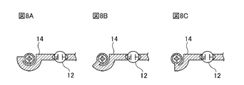
- FIG. 8A is a view (a view of approximately 180 degrees) showing Modification 3 of the conductor wiring 14.
- FIG. 8B is a view (a view of approximately 135 degrees) showing Modified Example 3 of the conductor wiring 14 .
- FIG. 8C is a view (a view of approximately 90 degrees) showing Modified Example 3 of the conductor wiring 14 .
- FIG. 9A is a perspective view of the configuration of the surge protection circuit 20 of Embodiment 2.
- FIG. 9B is a cross-sectional view showing the configuration of the surge protection circuit 20 of Embodiment 2.
- FIG. 10A is a perspective view showing the configuration of the surge protection circuit 30 of Embodiment 3.
- FIG. 10B is a cross-sectional view showing the configuration of the surge protection circuit 30 of Embodiment 3.
- FIG. 11A is a perspective view showing the configuration of the surge protection circuit 40 of Embodiment 4.
- FIG. 11B is a cross-sectional view showing the configuration of the surge protection circuit 40 of the fourth embodiment.
- FIG. 11 is a cross-sectional view showing a magnetic field generated by a surge protection circuit 40 of Embodiment 4;
- FIG. 9 is a cross-sectional view showing a magnetic field generated by a surge protection circuit 30 of Embodiment 3 of a comparative example;
- Embodiment 1 A first embodiment of a surge protection circuit according to the present disclosure will be described.
- FIG. 1 is a circuit diagram of equipment including the surge protection circuit of Embodiment 1.
- FIG. 1 is a circuit diagram of equipment including the surge protection circuit of Embodiment 1.
- the device KK of Embodiment 1 includes a printed circuit board 11, as shown in FIG.
- the printed circuit board 11 is provided with a circuit KR such as an electric circuit and an electronic circuit, and a varistor VR and a surge absorber 12 for protecting the circuit KR from lightning or the like.
- a conductor wiring 14 is also formed on the printed circuit board 11 .
- a rod-shaped member 13 is arranged between the printed circuit board 11 and the housing KT (shown in FIG. 2) of the device KK.
- the circuit KR is supplied with power, for example, single-phase AC 100 V, via the first terminal TN1 and the second terminal TN2, and the first power line PL1 and the second power line PL2.
- the varistor VR is connected between the first power line PL1 and the second power line PL2.
- Surge absorber 12, conductor wiring 14, and bar member 13 are connected in series between second power supply line PL2 and ground potential GL.
- the device KK more precisely, the housing KT of the device KK (illustrated in FIG. 2) is connected to the ground potential GL.
- a portion of the printed circuit board 11 , the surge absorber 12 , the cylindrical rod-shaped member 13 , and the conductor wiring 14 constitute the surge protection circuit 10 .
- FIG. 2A is a perspective view showing the configuration of the surge protection circuit 10 of Embodiment 1.
- FIG. 2A is a perspective view showing the configuration of the surge protection circuit 10 of Embodiment 1.
- FIG. 2B is a cross-sectional view showing the configuration of the surge protection circuit 10 of Embodiment 1 on the XZ plane 100 of FIG. 2A.
- the surge protection circuit 10 includes a printed circuit board 11, a surge absorber 12, a bar member 13, and conductor wiring 14, as shown in FIG. 2A.
- the surge protection circuit 10 corresponds to "surge protection circuit”
- the printed circuit board 11 corresponds to “printed circuit board”
- the surge absorber 12 corresponds to “surge absorber”
- the rod-shaped member 13 corresponds to "member”.
- the conductor wiring 14 corresponds to "conductor wiring”.
- the printed circuit board 11 is an insulator plate, as is conventionally known.
- a surge absorber 12 is arranged on the surface (XY plane) of the printed circuit board 11 .
- a conductor wiring 14 is formed on the surface of the printed board 11 , that is, on the upper surface of the printed board 11 .
- the printed circuit board 11 is provided with holes AN for fixing the printed circuit board 11 to the equipment KK with the rod-shaped member 13 .
- the surge absorber 12 is, for example, a two-terminal arrester.
- the surge absorber 12 has a gap between electrodes at both ends, and discharges a surge voltage caused by lightning or the like in the gap.
- the rod-shaped member 13 is a screw made of a conductive and magnetic material. Examples of the material include iron and some stainless steels having magnetism.
- the rod-shaped member 13 extends in a direction (Z-axis direction) orthogonal to the surface (XY plane) of the printed circuit board 11 .
- the conductor wiring 14 has one end connected to the surge absorber 12 and the other end connected to the bar member 13 .
- the surge absorber 12, the conductor wiring 14, and the bar member 13 are connected in series with each other.
- the conductor wiring 14 is also wired starting from the intersection point KTN between the surface (XY plane) of the printed circuit board 11 and the center line CS of the rod-shaped member 13 in the orthogonal direction (Z-axis direction).
- the conductor wiring 14 is further formed along at least part of a virtual spiral KRK centered on the intersection point KTN on the surface (XY plane) of the printed circuit board 11 .
- the conductor wiring 14 is formed so as to surround the rod-shaped member 13 .
- the conductor wiring 14 is, for example, a plane (XY plane) parallel to the surface (XY plane) of the printed circuit board 11 and imaginary in the printed circuit board 11. (not shown) and the center line CS of the rod-like member 13 may be set as the starting point.
- the intersection point KTN may exist within a layer of the printed circuit board 11 instead of existing on the surface of the printed circuit board 11 .
- the housing KT of the device KK is basically made of a conductive material, such as metal.
- a conductive material such as metal.
- Part KK1 is made of a conductive material.
- the portion KK1 described above is formed in a columnar shape extending in the orthogonal direction (Z-axis direction).
- the rod-shaped member 13 is screwed to a portion KK1 of the housing KT of the device KK via the hole AN of the printed circuit board 11 described above. Thereby, the printed circuit board 11 and the housing KT of the device KK are mechanically fixed. In addition to mechanically fixing the printed circuit board 11 and the device KK, the rod-shaped member 13 electrically connects the conductor wiring 14 on the printed circuit board 11 and the housing KT of the device KK.
- FIG. 1 is a perspective view showing the operation of the surge protection circuit 10 of Embodiment 1.
- FIG. 3A is a perspective view showing the operation of the surge protection circuit 10 of Embodiment 1.
- FIG. 3B is a cross-sectional view showing the operation of the surge protection circuit 10 of Embodiment 1.
- FIG. 3B is a cross-sectional view showing the operation of the surge protection circuit 10 of Embodiment 1.
- the surge absorber 12 reacts to the surge voltage, and the dotted arrow , a surge current SC flows. Specifically, the surge current SC passes from the varistor VR (shown in FIG. 1) to the device KK via the surge absorber 12, the conductor wiring 14, and the rod-shaped member 13, as indicated by the dotted arrow. It flows to the housing KT.
- ⁇ Effect of Embodiment 1> 4A is a perspective view showing the relationship between the surge current SC and the magnetic field JK of Embodiment 1.
- FIG. 4A is a perspective view showing the relationship between the surge current SC and the magnetic field JK of Embodiment 1.
- FIG. 4B is a cross-sectional view showing the relationship between the surge current SC and the magnetic field JK in Embodiment 1.
- FIG. 4B is a cross-sectional view showing the relationship between the surge current SC and the magnetic field JK in Embodiment 1.
- the surge protection circuit 10 of Embodiment 1 by adopting the configuration of the conductor wiring 14 of the rod-shaped member 13 described above, a larger space for arrangement is required in the space above the printed circuit board 11 than for the surge absorber 12 and the like. There is no need to place a coil to As a result, the surge protection circuit 10 of the first embodiment can be made smaller than conventional surge protection circuits.
- FIG. 5A is a diagram (a diagram of the configuration of Embodiment 1) showing a comparison between the surge protection circuit 10 of Embodiment 1 and a surge protection circuit of a comparative example.
- FIG. 5B is a diagram (a diagram of a configuration of a comparative example) showing a comparison between the surge protection circuit 10 of Embodiment 1 and a surge protection circuit of a comparative example.
- the surge protection circuit 10 of the first embodiment and the surge protection circuit of the comparative example each use an iron screw with a relative magnetic permeability of 1000 or more as the rod-shaped member 13 .
- the conductor wiring 14 is formed along the virtual spiral KRK in a small space around the rod-shaped member 13, and theoretically about 30 nH of inductance is generated.
- the conductor wiring 14X is not along the virtual spiral KRK but straight and folded. formed by
- the conductor wiring 14X has a wiring width of 3 mm, generally 0.6 nH/mm. As a result, the total length of the conductor wiring 14X (the length of the dashed-dotted line in FIG. 5B) is required to be approximately 50 mm. From this, it can be said that the space for forming the conductor wiring 14 in the surge protection circuit 10 of the first embodiment is smaller than the space for forming the conductor wiring 14X in the surge protection circuit of the comparative example.
- FIG. 6 shows Modification 1 of the conductor wiring 14 .
- the conductor wiring 14 may be wound multiple times, such as twice, instead of being wound only once (illustrated in FIG. 2A). This further increases the inductance of the conductor wiring 14, and as a result, it is possible to more strongly suppress a rapid change in the surge current SC.
- FIG. 7A is a diagram (surface diagram) showing Modified Example 2 of the conductor wiring 14.
- FIG. 7A is a diagram (surface diagram) showing Modified Example 2 of the conductor wiring 14.
- FIG. 7B is a view (back side view) showing Modification 2 of the conductor wiring 14.
- FIG. 7B specifically shows the rear surface of the printed circuit board 11 seen through from the front surface.
- the conductor wiring 14 is formed on both the front surface and the rear surface of the printed circuit board 11, which are two layers. good too.
- a conductor wiring 14A corresponding to half of the conductor wiring 14 is formed on the surface of the printed circuit board 11, and as shown in FIG. A conductor wiring 14B corresponding to the remaining half may be formed on the back surface of the printed circuit board 11 .
- the conductor wiring 14A and the conductor wiring 14B are connected by through holes TH1 and TH2 penetrating the printed circuit board 11, for example.
- the conductor wiring 14 may be formed on both sides of the multilayer printed circuit board 11 (not shown) and between the layers.
- FIG. 8A is a view (a view of about 180 degrees) showing Modification 3 of the conductor wiring 14.
- FIG. 8A is a view (a view of about 180 degrees) showing Modification 3 of the conductor wiring 14.
- FIG. 8B is a diagram (a diagram of about 135 degrees) showing Modification 3 of the conductor wiring 14.
- FIG. 8B is a diagram (a diagram of about 135 degrees) showing Modification 3 of the conductor wiring 14.
- FIG. 8C is a view (a view of about 90 degrees) showing Modification 3 of the conductor wiring 14.
- the conductor wiring 14 is formed along the virtual spiral KRK as shown in FIG. 8A. , and may be formed to a length corresponding to about 135 degrees along the imaginary spiral KRK, as shown in FIG. 8B, and further, As shown in FIG. 8C, it may be formed with a length corresponding to approximately 90 degrees along the virtual helix KRK.
- the inductance of the conductor wiring 14 is not increased to the extent that the conductor wiring 14 having a length corresponding to about 270 degrees in the first embodiment increases.
- the length, shape, etc. of the conductor wiring 14 can be appropriately adjusted from the viewpoint of the width of the space on the surface of the substrate 11 and the size of the inductance to be increased.
- the direction of the virtual spiral KRK in which the conductor wiring 14 is routed may be clockwise (for example, shown in FIG. 8) instead of counterclockwise from outside to inside (shown in FIG. 2A). .
- the conductor wiring 14 may be wound multiple times as described above (shown in FIG. 6), formed between planes and layers (shown in FIG. 7, etc.), and formed along a portion of the virtual spiral KRK. (illustrated in FIG. 8).
- the rod-shaped member 13 may have any shape as long as it has conductivity and magnetism.
- the rod-shaped member 13 may have a length that is the same as the length of the portion KK1, and It may have a length exceeding the length of said portion KK1.
- ⁇ Modification of surge absorber 12> instead of using an arrester as the surge absorber 12, another semiconductor element such as a varistor may be used, or both may be used together.
- Surge absorber 12 may be connected to a communication line such as a telephone line instead of first and second power lines PL1 and PL2 for supplying power.
- a communication line such as a telephone line
- a spacer separate from the device KK may be used.
- the housing KT of the device KK may have magnetism in addition to conductivity.
- the device KK may be supplied with three-phase AC power or DC power instead of being supplied with single-phase AC power from the first and second power lines PL1 and PL2.
- Embodiment 2 A second embodiment of the surge protection circuit will be described.
- FIG. 9A is a perspective view showing the configuration of the surge protection circuit 20 of Embodiment 2.
- FIG. 9A is a perspective view showing the configuration of the surge protection circuit 20 of Embodiment 2.
- FIG. 9B is a cross-sectional view showing the configuration of the surge protection circuit 20 of Embodiment 2 on the XZ plane 200 of FIG. 9A.
- the configuration of the surge protection circuit 20 of Embodiment 2 will be described with reference to FIGS. 9A and 9B.
- the surge protection circuit 20 of the second embodiment includes a printed circuit board 21, a surge absorber 22, a bar member 23, and a conductor wiring 24, like the surge protection circuit 10 of the first embodiment (shown in FIG. 2). include.
- the configurations and functions of the printed circuit board 21 and the surge absorber 22 of the second embodiment are basically the same as the configurations and functions of the printed circuit board 11 and the surge absorber 12 of the first embodiment.
- the rod-shaped member 23 of Embodiment 2 has conductivity and magnetism like the rod-shaped member 13 of Embodiment 1, but unlike the rod-shaped member 13 of Embodiment 1, it is a spacer instead of a screw.
- the rod-shaped member 23 has, for example, a columnar shape or a tubular shape.
- the rod-shaped member 23 is mechanically fixed to the equipment KK (not shown).
- the rod-shaped member 23 is also screwed through the hole AN of the printed circuit board 21 with a mounting screw 25 . Thereby, the printed circuit board 21 and the housing KT of the device KK are mechanically fixed.
- the mounting screws 25 have the mechanical fixing function described above.
- the mounting screw 25 does not need to be conductive and magnetic, unlike the bar member 13 of the first embodiment, that is, the conductive and magnetic screw. Therefore, the mounting screws 25 may be made of resin, for example.
- the conductor wiring 24 of the second embodiment has one end connected to the surge absorber 22 and the other end connected to the rod-shaped member 23 and surrounds the rod-shaped member 23, similarly to the conductor wiring 14 of the first embodiment. is formed as
- the conductor wiring 24 of the second embodiment is formed on the back surface of the printed circuit board 21 unlike the conductor wiring 14 of the first embodiment.
- a conductor wiring 24 is formed on the back surface of the printed circuit board 21 by mechanically fixing the rod-shaped member 23 and the device KK and screwing the mounting screws 25 through the holes AN of the printed circuit board 21. are electrically connected to the bar member 23 and the housing KT of the device KK.
- Embodiment 2 The operation of the surge protection circuit 20 of the second embodiment is similar to the operation of the surge protection circuit 10 of the first embodiment (shown in FIGS. 3 and 4).
- the conductor wiring 24 formed on the back surface of the printed circuit board 21 is connected to the rod-shaped member 23, more specifically, has conductivity and magnetism, and is connected between the printed circuit board 21 and the device KK. is directly and electrically connected to the rod-shaped member 23 which is a spacer of the . Therefore, unlike the rod-like member 13 of Embodiment 1, which is a conductive and magnetic screw, the mounting screw 25 of the second embodiment does not need to have conductivity and magnetism. As a result, for example, when selecting one type of mounting screw 25 from a plurality of types of mounting screw 25 candidates, it is not necessary to consider electrical properties such as conductivity and magnetism. As a result, it is possible to select one type of mounting screw 25 more freely than in the first embodiment, for example, only considering mechanical characteristics and workability of mechanical assembly. can be selected.
- the mounting screw 25 and the hole AN are not necessarily used if the conductor wiring 24 and the rod-shaped member 23 are electrically connected and the conductor wiring 24 is arranged so as to surround the rod-shaped member 23 .
- the portion of the upper surface where the rod-shaped member 23 contacts the printed circuit board 21 may be formed into a convex shape, and the convex upper surface portion may be used to position the rod-shaped member 23 on the printed circuit board 21 .
- the rod-shaped member 23 can be formed into a convex and threaded shape on the upper surface where the rod-shaped member 23 contacts the printed circuit board 21, and by passing a nut or the like through the convex and threaded upper surface, the printed circuit board can be mounted on the printed circuit board. 21 may be fixed.
- the mounting screw 25 may have a length equal to the length of the rod-shaped member 23 instead of having a length about half the length of the rod-shaped member 23, or may have a length equal to the length of the rod-shaped member 23. It may have a length exceeding the height.
- the conductor wiring 24 may be wound a plurality of times (shown in FIG. 6), or may be formed on both sides or between layers of the printed circuit board 21 (shown in FIG. 7). 180 degrees, 135 degrees, and 90 degrees along the virtual spiral KRK (shown in FIG. 8), or a combination thereof.
- Embodiment 3 A third embodiment of the surge protection circuit will be described.
- FIG. 10A is a perspective view showing the configuration of the surge protection circuit 30 of Embodiment 3.
- FIG. 10A is a perspective view showing the configuration of the surge protection circuit 30 of Embodiment 3.
- FIG. 10B is a cross-sectional view showing the configuration of the surge protection circuit 30 of Embodiment 3 on the XZ plane 300 of FIG. 10A.
- the surge protection circuit 30 of Embodiment 3 includes a printed circuit board 31, a surge absorber 32, a truncated conical trapezoidal member 33, and conductor wiring 34 .
- the configurations and functions of the printed circuit board 31 and the surge absorber 32 of the third embodiment are basically the same as the configurations and functions of the printed circuit board 11 and the surge absorber 12 of the first embodiment.
- the housing KT of the device KK of the third embodiment is different from the housing KT of the device KK of the first embodiment and is made of a material having conductivity and magnetism.
- the pedestal member 33 is a part of the housing KT of the device KK, and more specifically, it is a portion formed into a trapezoidal shape or the like by press working or the like from the housing KT of the device KK.
- a hole AN2 is provided in the upper surface of the platform member 33 .
- the printed circuit board 31 and the housing KT of the device KK are mechanically fixed by screwing the mounting screws 35 through the holes AN of the printed circuit board 31 and the holes AN2 of the pedestal member 33 .
- the mounting screw 35 does not need to have electrical conductivity and magnetism, so the material does not matter.
- Embodiment 3 The operation of the surge protection circuit 30 of the third embodiment is similar to the operation of the surge protection circuit 10 of the first embodiment (illustrated in FIGS. 3 and 4).
- a surge protection circuit 30 of the third embodiment has a platform member 33 instead of the rod-shaped member 23 of the second embodiment. Unlike the bar member 23 which is a spacer separate from the housing KT of the device KK, the platform member 33 is a part of the housing KT of the device KK, that is, is integral with the housing KT of the device KK. be. As a result, the surge protection circuit 30 of the third embodiment can reduce the number of parts to be mounted and the number of parts to be assembled, for example, compared to the surge protection circuit 20 of the second embodiment.
- the pedestal member 33 may be provided by welding or attaching to the housing KT of the device KK with a conductive adhesive instead of being provided by molding such as press working as described above, or may be provided by press fitting. .
- the mounting screw 35 does not have to penetrate the platform member 33 instead of penetrating the platform member 33 as long as the printed circuit board 31 can be fixed to the platform member 33 .
- the convex upper surface portion of the platform member 33 may be used to position the platform member 33 on the printed circuit board 31, or the protrusion of the platform member 33 may be used.
- the printed circuit board 31 may be fixed by passing a nut or the like through the portion of the upper surface that is formed into a shape and a threaded shape.
- the conductor wiring 34 may be wound a plurality of times (shown in FIG. 6), or may be formed on both sides or between layers of the printed circuit board 21 (shown in FIG. 7). 180 degrees along the virtual spiral KRK (shown in FIG. 8), or a combination thereof.
- Embodiment 4 A fourth embodiment of the surge protection circuit will be described.
- FIG. 11A is a perspective view showing the configuration of the surge protection circuit 40 of Embodiment 4.
- FIG. 11A is a perspective view showing the configuration of the surge protection circuit 40 of Embodiment 4.
- FIG. 11B is a cross-sectional view showing the configuration of the surge protection circuit 40 of Embodiment 4 on the XZ plane 400 of FIG. 11A.
- the configuration of the surge protection circuit 40 of Embodiment 4 will be described with reference to FIGS. 11A and 11B.
- the surge protection circuit 40 of Embodiment 4 includes a printed circuit board 41, a surge absorber 42, a platform member 43, conductor wiring 44, including.
- the pedestal member 43 of the fourth embodiment differs from the pedestal member 33 of the third embodiment in that the outer diameter 43KE of the upper surface of the pedestal member 43 is larger than the inner diameter 44KE of the conductor wiring 44 .
- the outer diameter 43KE of the upper surface of the platform member 43 is the diameter of the upper surface of the platform member 43, which has a substantially circular shape.
- the inner diameter 44KE of the conductor wiring 44 is the point at which the conductor wiring 44, which is spirally formed along the imaginary spiral shape KRK, bends at a substantially right angle toward the center line CS. It is approximately twice the distance 44KY between PT and the centerline CS.
- the outer diameter 43KE of the upper surface of the pedestal member 43 corresponds to "the diameter of the upper surface of the member”.
- the inner diameter 44KE of the conductor wiring 44 corresponds to "the diameter of the virtual circle defined by at least part of the virtual spiral of the conductor wiring”.
- the platform member 43 is also provided with a notch 46 as shown in FIG. 11B. Notch 46 ensures that platform member 43 is in principle not electrically connected to the entire conductor trace 44, as shown in FIG. As an exception, the shaped member 43 has a shape to ensure that it is electrically connected only to the circular region RY of the conductor wiring 44 that is in the vicinity of the mounting screw 45 .
- Embodiment 4 The operation of the surge protection circuit 40 of the fourth embodiment is similar to the operation of the surge protection circuit 10 of the first embodiment (illustrated in FIGS. 3 and 4).
- FIG. 12 shows the magnetic field generated by the surge protection circuit 40 of the fourth embodiment.
- FIG. 13 shows the magnetic field generated by the surge protection circuit 30 of Embodiment 3 of the comparative example.
- Embodiment 3 which is a comparative example, as shown in FIG.
- the inner diameter is smaller than 34KE.
- the surge protection circuit 40 of the fourth embodiment in contrast to the surge protection circuit 30 of the third embodiment, in the surge protection circuit 40 of the fourth embodiment, as described above with reference to FIG. greater than As a result, all of the magnetic field JK ⁇ b>4 generated by the surge current SC flowing through the conductor wiring 44 passes through the upper surface of the platform member 43 . Therefore, in the surge protection circuit 40 of the fourth embodiment, the inductance can be made larger than in the surge protection circuit 30 of the third embodiment, and as a result, rapid changes in the surge current SC can be further suppressed. becomes possible.
- an insulating sheet member may be arranged between the conductor wiring 44 and the pedestal member 43 instead of the notch 46 described above.
- the notch 46 may not be provided.
- a surge protection circuit according to the present disclosure can be used, for example, in a surge protection system that protects a semiconductor element for protecting a circuit and elements from a lightning strike or the like from a sudden increase in current caused by the lightning strike or the like.
Landscapes
- Engineering & Computer Science (AREA)
- Microelectronics & Electronic Packaging (AREA)
- Power Engineering (AREA)
- Emergency Protection Circuit Devices (AREA)
Abstract
Description
〈実施形態1〉
本開示に係るサージ保護回路の実施形態1について説明する。
図1は、実施形態1のサージ保護回路を含む機器の回路図である。
図3Aは、実施形態1のサージ保護回路10の動作を示す斜視図である。
図4Aは、実施形態1のサージ電流SCと磁界JKとの関係を示す斜視図である。
図5Aは、実施形態1のサージ保護回路10と比較例のサージ保護回路との比較を示す図(実施形態1の構成の図)である。
〈導体配線14の変形例〉
図6は、導体配線14の変形例1を示す。
棒状部材13は、導電性及び磁性を有しさえすれば、形状を問わず、具体的には、ネジであることに代えて、釘、角柱、ブロック等のいずれかであってもよい。
サージアブソーバ12としてアレスタを使用することに代えて、バリスタ等の他の半導体素子を使用してもよく、または、両者を併用してもよい。
〈機器KKの変形例〉
機器KKの筐体KTの一部分KK1を用いることに代えて、機器KKとは別体であるスペーサを用いてもよい。
〈実施形態2〉
サージ保護回路の実施形態2について説明する。
図9Aは、実施形態2のサージ保護回路20の構成を示す斜視図である。
実施形態2のサージ保護回路20の動作は、実施形態1のサージ保護回路10の動作(図3、図4に図示。)と同様である。
実施形態2のサージ保護回路20では、プリント基板21の裏面に形成された導体配線24が、棒状部材23と、より詳しくは、導電性及び磁性を有し、かつ、プリント基板21及び機器KK間のスペーサである棒状部材23と、直接的に電気的に接続されている。従って、実施形態2の取付用ネジ25は、導電性及び磁性を有するネジである実施形態1の棒状部材13とは相違して、導電性及び磁性を有することを要しない。これにより、例えば、複数の種類の取付用ネジ25の候補から一種類の取付用ネジ25を選択するときに、導電性及び磁性等の電気的特性を考慮する必要が無い。その結果、前記一種類の取付用ネジ25を選択することを、実施形態1に比してより自由に行うことができ、例えば、機械的特性、機械的な組み立ての作業性のみを考慮して選択することができる。
〈取付用ネジ25の変形例〉
取付用ネジ25及び孔ANは、導体配線24と棒状部材23とが電気的に接続され、かつ、導体配線24が棒状部材23を囲むように配置されれば、必ずしも使用することを要しない。例えば、棒状部材23がプリント基板21と接触する上面の部分を凸形状に成形し、当該凸形状である上面の部分を、プリント基板21に棒状部材23を位置決めするために用いてもよい。例えば、また、棒状部材23がプリント基板21と接触する上面の部分を凸形状かつネジ切り形状に成形し、当該凸形状かつネジ切り形状である上面の部分にナット等を通すことにより、プリント基板21を固定してもよい。
導体配線24は、実施形態1の導体配線14の変形例と同様に、複数回巻いてもよく(図6に図示。)、プリント基板21の両面、層間に形成してもよく(図7に図示等。)、仮想螺旋形KRKに沿って約180度、約135度、約90度に相当する長さに形成してもよく(図8に図示。)、これらを組み合わせてもよい。
〈実施形態3〉
サージ保護回路の実施形態3について説明する。
図10Aは、実施形態3のサージ保護回路30の構成を示す斜視図である。
実施形態3のサージ保護回路30の動作は、実施形態1のサージ保護回路10の動作(図3、図4に図示。)と同様である。
実施形態3のサージ保護回路30では、実施形態2の棒状部材23に代えて、台状部材33を有する。台状部材33は、機器KKの筐体KTとは別体なスペーサである棒状部材23と相違して、機器KKの筐体KTの一部分であり、即ち、機器KKの筐体KTと同体である。これにより、実施形態3のサージ保護回路30は、実施形態2のサージ保護回路20に比して、例えば、実装すべき部品の点数、組み立てるべき部品の点数を低減することができる。
〈台状部材33の変形例〉
台状部材33は、上記したプレス加工等の成形により設けることに代えて、機器KKの筐体KTに溶接や導電性接着剤により取り付けることにより設けてもよく、また、圧入によって設けてもよい。
取付用ネジ35は、プリント基板31を台状部材33に固定することができれば、台状部材33を貫通することに代えて、台状部材33を貫通しなくてもよい。
導体配線34は、実施形態1の導体配線14の変形例と同様に、複数回巻いてもよく(図6に図示。)、プリント基板21の両面、層間に形成してもよく(図7に図示等。)、仮想螺旋形KRKに沿って約180度等に相当する長さに形成してもよく(図8に図示。)、これらを組み合わせてもよい。
〈実施形態4〉
サージ保護回路の実施形態4について説明する。
図11Aは、実施形態4のサージ保護回路40の構成を示す斜視図である。
実施形態4のサージ保護回路40の動作は、実施形態1のサージ保護回路10の動作(図3、図4に図示。)と同様である。
図12は、実施形態4のサージ保護回路40が生起させる磁界を示す。
〈切り欠き46の変形例〉
導体配線44及び台状部材43間の絶縁を確保すべく、上記した切り欠き46に代えて、導体配線44及び台状部材43間に絶縁性のシート部材を配置してもよい。
Claims (5)
- プリント基板と、
前記プリント基板上に配置されたサージアブソーバと、
前記プリント基板の表面と直交する方向に伸びる、導電性及び磁性を有する部材と、
一端が前記サージアブソーバに接続され、他端が前記部材に接続された導体配線であって、前記プリント基板の表面に平行な平面と、前記直交する方向についての前記部材の中心線との交点を起点に、前記平行な面における前記交点を中心とする仮想螺旋形の少なくとも一部に沿って形成された前記導体配線と、
を含むサージ保護回路。 - 前記部材は、円柱状である請求項1に記載のサージ保護回路。
- 前記部材は、円錐台状である請求項1に記載のサージ保護回路。
- 前記部材の上面の径が、前記導体配線の前記仮想螺旋形の少なくとも一部により規定される仮想円の径より大きい
請求項3に記載のサージ保護回路。 - プリント基板上に配置されたサージアブソーバに接続された導体配線であって、前記プリント基板の表面に平行な平面と、前記直交する方向についての前記部材の中心線との交点を起点に、前記平行な面における前記交点を中心とする仮想螺旋形の少なくとも一部に沿って形成された前記導体配線にサージ電流が流れることにより生起する磁界を、前記導体配線に接続され、前記プリント基板の表面と直交する方向に伸び、かつ、導電性及び磁性を有する部材に通させるサージ保護方法。
Priority Applications (5)
| Application Number | Priority Date | Filing Date | Title |
|---|---|---|---|
| CN202180095172.XA CN116897484A (zh) | 2021-03-11 | 2021-03-11 | 浪涌保护电路和浪涌保护方法 |
| DE112021006782.6T DE112021006782T5 (de) | 2021-03-11 | 2021-03-11 | Überspannungsschutzschaltung und überspannungsschutzverfahren |
| JP2023505003A JP7301250B2 (ja) | 2021-03-11 | 2021-03-11 | サージ保護回路及びサージ保護方法 |
| PCT/JP2021/009713 WO2022190306A1 (ja) | 2021-03-11 | 2021-03-11 | サージ保護回路及びサージ保護方法 |
| US18/216,123 US20230345628A1 (en) | 2021-03-11 | 2023-06-29 | Surge protection circuit and surge protection method |
Applications Claiming Priority (1)
| Application Number | Priority Date | Filing Date | Title |
|---|---|---|---|
| PCT/JP2021/009713 WO2022190306A1 (ja) | 2021-03-11 | 2021-03-11 | サージ保護回路及びサージ保護方法 |
Related Child Applications (1)
| Application Number | Title | Priority Date | Filing Date |
|---|---|---|---|
| US18/216,123 Continuation US20230345628A1 (en) | 2021-03-11 | 2023-06-29 | Surge protection circuit and surge protection method |
Publications (1)
| Publication Number | Publication Date |
|---|---|
| WO2022190306A1 true WO2022190306A1 (ja) | 2022-09-15 |
Family
ID=83226493
Family Applications (1)
| Application Number | Title | Priority Date | Filing Date |
|---|---|---|---|
| PCT/JP2021/009713 WO2022190306A1 (ja) | 2021-03-11 | 2021-03-11 | サージ保護回路及びサージ保護方法 |
Country Status (5)
| Country | Link |
|---|---|
| US (1) | US20230345628A1 (ja) |
| JP (1) | JP7301250B2 (ja) |
| CN (1) | CN116897484A (ja) |
| DE (1) | DE112021006782T5 (ja) |
| WO (1) | WO2022190306A1 (ja) |
Citations (6)
| Publication number | Priority date | Publication date | Assignee | Title |
|---|---|---|---|---|
| JPH04284686A (ja) * | 1991-03-14 | 1992-10-09 | Sharp Corp | 電気回路の製造方法 |
| JPH05219648A (ja) * | 1992-02-06 | 1993-08-27 | Ngk Insulators Ltd | 半導体式避雷装置 |
| JPH0567042U (ja) * | 1992-02-14 | 1993-09-03 | 株式会社ジャルコ | 回路基板 |
| JPH0718409U (ja) * | 1993-08-24 | 1995-03-31 | 森宮電機株式会社 | ノイズ吸収機能を付加したプリント基板保持機構 |
| JPH09199818A (ja) * | 1996-01-12 | 1997-07-31 | Canon Inc | グランド間接続構造 |
| JPH1051171A (ja) * | 1996-07-31 | 1998-02-20 | Pfu Ltd | 電子機器用筐体 |
Family Cites Families (4)
| Publication number | Priority date | Publication date | Assignee | Title |
|---|---|---|---|---|
| JPS5219648A (en) | 1975-08-08 | 1977-02-15 | Sumitomo Chem Co Ltd | Preparation of 1-nitroanthraquinone |
| US7151298B1 (en) | 1999-12-20 | 2006-12-19 | Advanced Micro Devices, Inc. | Electrostatic discharge protection network having distributed components |
| JP6843312B1 (ja) | 2020-03-25 | 2021-03-17 | 三菱電機株式会社 | 回路基板及び電子機器 |
| CN217984533U (zh) | 2022-07-22 | 2022-12-06 | 珠海市睿特光电技术有限公司 | 滤波网络及装置 |
-
2021
- 2021-03-11 WO PCT/JP2021/009713 patent/WO2022190306A1/ja active Application Filing
- 2021-03-11 DE DE112021006782.6T patent/DE112021006782T5/de active Granted
- 2021-03-11 JP JP2023505003A patent/JP7301250B2/ja active Active
- 2021-03-11 CN CN202180095172.XA patent/CN116897484A/zh active Pending
-
2023
- 2023-06-29 US US18/216,123 patent/US20230345628A1/en active Pending
Patent Citations (6)
| Publication number | Priority date | Publication date | Assignee | Title |
|---|---|---|---|---|
| JPH04284686A (ja) * | 1991-03-14 | 1992-10-09 | Sharp Corp | 電気回路の製造方法 |
| JPH05219648A (ja) * | 1992-02-06 | 1993-08-27 | Ngk Insulators Ltd | 半導体式避雷装置 |
| JPH0567042U (ja) * | 1992-02-14 | 1993-09-03 | 株式会社ジャルコ | 回路基板 |
| JPH0718409U (ja) * | 1993-08-24 | 1995-03-31 | 森宮電機株式会社 | ノイズ吸収機能を付加したプリント基板保持機構 |
| JPH09199818A (ja) * | 1996-01-12 | 1997-07-31 | Canon Inc | グランド間接続構造 |
| JPH1051171A (ja) * | 1996-07-31 | 1998-02-20 | Pfu Ltd | 電子機器用筐体 |
Also Published As
| Publication number | Publication date |
|---|---|
| CN116897484A (zh) | 2023-10-17 |
| JP7301250B2 (ja) | 2023-06-30 |
| US20230345628A1 (en) | 2023-10-26 |
| JPWO2022190306A1 (ja) | 2022-09-15 |
| DE112021006782T5 (de) | 2023-11-16 |
Similar Documents
| Publication | Publication Date | Title |
|---|---|---|
| KR100668977B1 (ko) | 써지전압 보호용 소자 | |
| US7492246B2 (en) | Winding structure of transformer | |
| KR20060136276A (ko) | 써지전압 보호용 소자 | |
| CN103167721A (zh) | 印刷电路板 | |
| JP6800783B2 (ja) | 保護装置 | |
| WO2022190306A1 (ja) | サージ保護回路及びサージ保護方法 | |
| JP2005203789A (ja) | 高電流フィードスルーデバイス | |
| US6178078B1 (en) | Discharge gap device and its mounting structure | |
| KR102202405B1 (ko) | 인쇄회로기판용 스파크 방지소자 | |
| JP6274369B1 (ja) | 携帯無線端末 | |
| JP2007067993A (ja) | アンテナ装置およびアンテナ用素子 | |
| JP6960588B2 (ja) | マルチバンド対応アンテナ及び無線通信装置 | |
| KR102165964B1 (ko) | 프린트 기판 | |
| JP7118317B1 (ja) | 電気電子機器 | |
| US7085115B2 (en) | Non-ferrous surge biasing coil having multiple pairs of coils positioned at angles to one another | |
| JP2019121652A (ja) | 実装基板及び電子機器 | |
| JP2019213186A (ja) | 電子部品及び電子制御ユニット | |
| WO2022186078A1 (ja) | チョークコイル装置及び電子装置 | |
| US9640970B2 (en) | Over-voltage protection device having a coil assembly | |
| EP1317170A2 (en) | Shielding structure for resonant circuit | |
| JP5966137B2 (ja) | 通信路用サージ保護装置 | |
| JP2019140135A (ja) | プリント配線板及、プリント回路板及び電子装置 | |
| JP2022142669A (ja) | ノイズフィルタ | |
| JP3498889B2 (ja) | 複合型サージ吸収器 | |
| JP2001291980A (ja) | フレームアース接続構造 |
Legal Events
| Date | Code | Title | Description |
|---|---|---|---|
| 121 | Ep: the epo has been informed by wipo that ep was designated in this application |
Ref document number: 21930159 Country of ref document: EP Kind code of ref document: A1 |
|
| ENP | Entry into the national phase |
Ref document number: 2023505003 Country of ref document: JP Kind code of ref document: A |
|
| WWE | Wipo information: entry into national phase |
Ref document number: 202180095172.X Country of ref document: CN |
|
| WWE | Wipo information: entry into national phase |
Ref document number: 112021006782 Country of ref document: DE |
|
| 122 | Ep: pct application non-entry in european phase |
Ref document number: 21930159 Country of ref document: EP Kind code of ref document: A1 |