WO2022186190A1 - 積層部品の整列方法および積層セラミック電子部品の製造方法 - Google Patents
積層部品の整列方法および積層セラミック電子部品の製造方法 Download PDFInfo
- Publication number
- WO2022186190A1 WO2022186190A1 PCT/JP2022/008563 JP2022008563W WO2022186190A1 WO 2022186190 A1 WO2022186190 A1 WO 2022186190A1 JP 2022008563 W JP2022008563 W JP 2022008563W WO 2022186190 A1 WO2022186190 A1 WO 2022186190A1
- Authority
- WO
- WIPO (PCT)
- Prior art keywords
- laminated
- aligning
- magnetic field
- laminated parts
- upper member
- Prior art date
Links
- 239000000919 ceramic Substances 0.000 title claims description 48
- 238000000034 method Methods 0.000 title claims description 45
- 238000004519 manufacturing process Methods 0.000 title claims description 23
- 230000005291 magnetic effect Effects 0.000 claims abstract description 78
- 230000004907 flux Effects 0.000 claims abstract description 20
- 239000000696 magnetic material Substances 0.000 claims abstract description 10
- 230000005294 ferromagnetic effect Effects 0.000 claims description 12
- 230000009471 action Effects 0.000 claims description 8
- 239000011230 binding agent Substances 0.000 claims description 8
- 239000007769 metal material Substances 0.000 claims description 7
- 238000003475 lamination Methods 0.000 claims description 4
- 239000013013 elastic material Substances 0.000 claims description 2
- 238000005245 sintering Methods 0.000 claims 1
- 239000010410 layer Substances 0.000 description 57
- 239000002243 precursor Substances 0.000 description 34
- 238000010586 diagram Methods 0.000 description 27
- 239000011241 protective layer Substances 0.000 description 18
- PXHVJJICTQNCMI-UHFFFAOYSA-N Nickel Chemical compound [Ni] PXHVJJICTQNCMI-UHFFFAOYSA-N 0.000 description 14
- 239000003985 ceramic capacitor Substances 0.000 description 14
- 238000010304 firing Methods 0.000 description 12
- 238000005520 cutting process Methods 0.000 description 10
- 238000005498 polishing Methods 0.000 description 8
- 239000002245 particle Substances 0.000 description 7
- 239000002002 slurry Substances 0.000 description 7
- 229910052759 nickel Inorganic materials 0.000 description 6
- 239000000463 material Substances 0.000 description 5
- 229920005992 thermoplastic resin Polymers 0.000 description 5
- 239000006061 abrasive grain Substances 0.000 description 4
- 239000000853 adhesive Substances 0.000 description 4
- 230000001070 adhesive effect Effects 0.000 description 4
- 229910010293 ceramic material Inorganic materials 0.000 description 4
- 238000001035 drying Methods 0.000 description 3
- 230000005389 magnetism Effects 0.000 description 3
- 239000000843 powder Substances 0.000 description 3
- 230000008569 process Effects 0.000 description 3
- 238000013459 approach Methods 0.000 description 2
- 239000003990 capacitor Substances 0.000 description 2
- 239000003989 dielectric material Substances 0.000 description 2
- 238000010030 laminating Methods 0.000 description 2
- 229910052751 metal Inorganic materials 0.000 description 2
- 239000002184 metal Substances 0.000 description 2
- 238000007639 printing Methods 0.000 description 2
- 229920005989 resin Polymers 0.000 description 2
- 239000011347 resin Substances 0.000 description 2
- 238000007650 screen-printing Methods 0.000 description 2
- 230000007704 transition Effects 0.000 description 2
- 229920006311 Urethane elastomer Polymers 0.000 description 1
- 238000005299 abrasion Methods 0.000 description 1
- 239000000654 additive Substances 0.000 description 1
- 230000000996 additive effect Effects 0.000 description 1
- 229910045601 alloy Inorganic materials 0.000 description 1
- 239000000956 alloy Substances 0.000 description 1
- 229910052782 aluminium Inorganic materials 0.000 description 1
- XAGFODPZIPBFFR-UHFFFAOYSA-N aluminium Chemical compound [Al] XAGFODPZIPBFFR-UHFFFAOYSA-N 0.000 description 1
- 239000011324 bead Substances 0.000 description 1
- 229910052802 copper Inorganic materials 0.000 description 1
- 230000007547 defect Effects 0.000 description 1
- 230000005347 demagnetization Effects 0.000 description 1
- 229910003460 diamond Inorganic materials 0.000 description 1
- 239000010432 diamond Substances 0.000 description 1
- 239000007772 electrode material Substances 0.000 description 1
- 238000005516 engineering process Methods 0.000 description 1
- 238000009415 formwork Methods 0.000 description 1
- 238000007646 gravure printing Methods 0.000 description 1
- 230000002706 hydrostatic effect Effects 0.000 description 1
- 230000005415 magnetization Effects 0.000 description 1
- 150000002739 metals Chemical class 0.000 description 1
- 239000011812 mixed powder Substances 0.000 description 1
- 239000011268 mixed slurry Substances 0.000 description 1
- 238000000465 moulding Methods 0.000 description 1
- 239000003960 organic solvent Substances 0.000 description 1
- 229910052763 palladium Inorganic materials 0.000 description 1
- 239000004014 plasticizer Substances 0.000 description 1
- 238000007517 polishing process Methods 0.000 description 1
- 229920002037 poly(vinyl butyral) polymer Polymers 0.000 description 1
- 229920002379 silicone rubber Polymers 0.000 description 1
- 229910052709 silver Inorganic materials 0.000 description 1
- 229910000679 solder Inorganic materials 0.000 description 1
- 239000002904 solvent Substances 0.000 description 1
- 239000000758 substrate Substances 0.000 description 1
Images


Classifications
-
- H—ELECTRICITY
- H01—ELECTRIC ELEMENTS
- H01G—CAPACITORS; CAPACITORS, RECTIFIERS, DETECTORS, SWITCHING DEVICES, LIGHT-SENSITIVE OR TEMPERATURE-SENSITIVE DEVICES OF THE ELECTROLYTIC TYPE
- H01G13/00—Apparatus specially adapted for manufacturing capacitors; Processes specially adapted for manufacturing capacitors not provided for in groups H01G4/00 - H01G11/00
-
- H—ELECTRICITY
- H01—ELECTRIC ELEMENTS
- H01G—CAPACITORS; CAPACITORS, RECTIFIERS, DETECTORS, SWITCHING DEVICES, LIGHT-SENSITIVE OR TEMPERATURE-SENSITIVE DEVICES OF THE ELECTROLYTIC TYPE
- H01G4/00—Fixed capacitors; Processes of their manufacture
- H01G4/002—Details
- H01G4/018—Dielectrics
- H01G4/06—Solid dielectrics
- H01G4/08—Inorganic dielectrics
- H01G4/12—Ceramic dielectrics
- H01G4/1209—Ceramic dielectrics characterised by the ceramic dielectric material
-
- H—ELECTRICITY
- H01—ELECTRIC ELEMENTS
- H01G—CAPACITORS; CAPACITORS, RECTIFIERS, DETECTORS, SWITCHING DEVICES, LIGHT-SENSITIVE OR TEMPERATURE-SENSITIVE DEVICES OF THE ELECTROLYTIC TYPE
- H01G4/00—Fixed capacitors; Processes of their manufacture
- H01G4/30—Stacked capacitors
Definitions
- the present disclosure relates to a method for aligning laminated components and a method for manufacturing laminated ceramic electronic components.
- Patent Document 1 An example of conventional technology is described in Patent Document 1.
- a method for aligning laminated parts of the present disclosure includes: a support member made of a non-magnetic material and having a horizontally parallel and flat support surface; A rectangular parallelepiped laminated component in which a plurality of ceramic green sheets and ferromagnetic electrode layers are alternately laminated in a space defined by an upper member provided at a predetermined distance from the surface. , exert a magnetic field whose magnetic flux lines intersect said support surface to align the laminate components.
- the manufacturing method of the laminated ceramic component of the present disclosure includes the method of aligning the laminated components described above, and after processing the surfaces of the laminated components aligned in the same direction, the laminated components are fired.
- FIG. 1 is a perspective view of an example of a laminated ceramic capacitor
- FIG. FIG. 3 is a diagram showing a base component before firing
- 1 is a perspective view showing a precursor of a base component
- FIG. FIG. 2 is an enlarged cross-sectional view schematically showing an element precursor
- Fig. 4 shows the state of the base part placed on the support member
- Fig. 4 shows the state of the base part placed on the support member
- It is a schematic diagram showing a state of forming a component assembly. It is a schematic diagram showing a state of fixing the base component.
- FIG. 1 is a schematic diagram showing a method of manufacturing a laminated component
- FIG. 1 is a schematic diagram showing a method of manufacturing a laminated component
- FIG. 1 is a schematic diagram showing a method of manufacturing a laminated component
- FIG. 4 is a schematic diagram showing how stacked components are aligned
- FIG. 4 is a schematic diagram showing how stacked components are aligned
- FIG. 4 is a schematic diagram showing how stacked components are aligned
- FIG. 4 is a schematic diagram showing how stacked components are aligned
- FIG. 4 is a schematic diagram showing how stacked components are aligned
- 1 is a schematic diagram showing a method of manufacturing a laminated component
- FIG. 1 is a schematic diagram showing a method of manufacturing a laminated component
- FIG. 1 is a schematic diagram showing a method of manufacturing a laminated component
- FIG. 1 is a schematic diagram showing a method of manufacturing a laminated component
- FIG. 1 is a schematic diagram showing a method of manufacturing
- FIG. 1 is a schematic diagram showing a method of manufacturing a laminated component
- FIG. FIG. 4 is a schematic diagram showing another method of manufacturing a laminated component
- FIG. 4 is a schematic diagram showing another method of manufacturing a laminated component
- FIG. 4 is a schematic diagram showing another method of manufacturing a laminated component
- FIG. 4 is a schematic diagram showing another method of aligning laminated components
- FIG. 4 is a schematic diagram showing another method of aligning laminated components
- FIG. 4 is a schematic diagram showing another method of manufacturing a laminated component
- FIG. 4 is a schematic diagram showing another method of manufacturing a laminated component
- FIG. 11 is a perspective view showing another example of the upper member
- a step of aligning the surfaces to be machined is required.
- a substantially rectangular chip component with lead-out electrodes of internal electrodes exposed at the ends in the width direction is accommodated in a pocket of a pallet having a concave shape, and a magnet is moved along the bottom surface outside the palette to move the chip component.
- the direction of the chip component is aligned by sucking and overturning the inside of the pocket (see Patent Document 1).
- Patent Literature 1 The smaller the base parts, the more difficult it is to align the surfaces to be processed.
- the alignment method described in Patent Literature 1 requires an operation to put the chip component into the pocket, and there is a problem that this operation becomes more complicated as the base component becomes smaller.
- multilayer ceramic capacitor will be described as an example of a multilayer ceramic electronic component, but the multilayer ceramic components to be disclosed are not limited to multilayer ceramic capacitors, and include multilayer piezoelectric elements, multilayer thermistor elements, and multilayer chip coils. , and various multilayer ceramic components such as ceramic multilayer substrates.
- FIG. 1 is a perspective view of an example of a laminated ceramic capacitor.
- 2 is a perspective view schematically showing an element component of the multilayer ceramic capacitor of FIG. 1.
- FIG. FIG. 2 is a diagram showing a base component before firing. It should be noted that although the fired body part has shrunk due to firing, it has the same structure as the body part before fired, so it can be said that FIG. 2 shows the fired body part.
- 3 is a perspective view showing a precursor of the base component of FIG. 2; FIG. In the following, the precursor of the elemental part is sometimes referred to as an elemental precursor.
- a multilayer ceramic capacitor 1 has a base component 2 and external electrodes 3 .
- the base component 2 has a substantially rectangular parallelepiped shape, as shown in FIG.
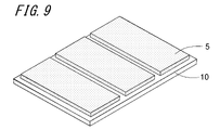
- the element part 2 is made of dielectric ceramics 4 and has a plurality of internal electrode layers 5 connected to the external electrodes 3 .
- the external electrodes 3 are arranged on a pair of end surfaces of the base component 2 and extend around other adjacent surfaces.
- a plurality of internal electrode layers 5 extend inward from a pair of end surfaces of the base component 2 and are alternately laminated without being in contact with each other.
- the internal electrode layers 5 are, for example, ferromagnetic layers containing a ferromagnetic metal material.
- the external electrode 3 is composed of a base layer connected to the base component 2 and a plated outer layer that facilitates solder mounting of the external wiring to the external electrode 3 .
- the base layer may be applied and baked onto the base component 2 after firing.
- the base layer may be disposed on the base component 2 before firing and fired at the same time as the base component 2 .
- the underlying layer and the plated outer layer may be multiple layers according to the required functions.
- the external electrode 3 may be configured to have an underlying layer and a conductive resin layer without having a plated outer layer.
- the base component 2 has a base precursor 13 and a protective layer 6, as shown in FIGS.
- the body precursor 13 has a substantially rectangular parallelepiped shape, as shown in FIG.
- the body precursor 13 has surfaces 7 facing each other, end surfaces 8 facing each other, and side surfaces 9 facing each other.
- the base body part 2 if the long side dimension of the face 7 is a, the width dimension is b, and the dimension in the stacking direction as the thickness is c, the relationship is, for example, a>b ⁇ c.
- the internal electrode layers 5 are exposed on the end faces 8 and side faces 9 of the element precursor 13 .
- the protective layer 6 is arranged on the side surface 9 of the element precursor 13 .
- the protective layer 6 prevents an electrical short circuit between the internal electrode layers 5 exposed on the first end surface 8A and the internal electrode layers 5 exposed on the second end surface 8B.
- the protective layer 6 physically protects the exposed portion of the internal electrode layer 5 on the side surface 9 of the element body precursor 13 .
- the protective layer 6 is applied last in making the base part 2 .
- the protective layer 6 protects the internal electrode layers 5 exposed on the side surfaces 9 of the body precursor 13 .
- the protective layer 6 may consist of a ceramic material. In this case, the protective layer 6 can have insulating properties and high mechanical strength.
- a ceramic material for the protective layer 6 is usually provided on the pre-firing body precursor 13 . In FIG. 2, the boundary between the element body precursor 13 and the protective layer 6 is indicated by a two-dot chain line, but the actual boundary does not appear clearly
- the precursor base 13 which is its precursor, was also described. .
- FIG. 4 is an enlarged cross-sectional view schematically showing the element precursor.
- Layers of ceramic green sheets 10 and internal electrode layers 5 are alternately laminated. Since the ceramic powder and the metal powder are not yet sintered by firing, the ceramic green sheet 10 is in a state in which the dielectric ceramic particles 35 are dispersed in the organic binder, and the internal electrode layers 5 are similarly in the organic binder. Nickel particles 36 are in a dispersed state.
- the magnetic susceptibility of the internal electrode layers 5 must be increased in order to apply a magnetic field to the internal electrode layers 5 . Since the nickel particles 36 of the internal electrode layer 5 are surrounded by the organic binder, most of them are not in contact with each other. In order to increase the magnetic susceptibility of the internal electrode layers 5, the volume ratio of the organic binder should be 1.5 times or less that of the ferromagnetic metal material, nickel particles.
- Figures 5A and 5B show the state of the base part placed on the support member. As shown in FIG. 5A, even when the blank parts 2 are placed on the support member 16 without intentional alignment of the blank parts 2, most of the blank parts 2 are the widest.
- the plane 7 is oriented parallel to the support surface 16 a of the support member 16 .
- the base component 2 when a magnetic field in which the magnetic flux lines 18 intersect the support surface 16a is applied to the base component 2 in the state of FIG. is parallel to the lines of magnetic flux 18.
- the base component 2 rotates so that the thickness direction of the internal electrode layers 5 is perpendicular to the magnetic flux lines 18 .
- the base component 2 is in either a state in which the side surfaces 9 are parallel to the support surface 16a (first state) or a state in which the end surfaces 8 are parallel to the support surface 16a (second state).
- processing treatment such as forming a protective layer 6 on the side surface 9 is applied to the base component 2, and all the base components 2 are oriented so as to be in the first state. is required.
- the two states of the base component 2 coexist, and it is difficult to align the orientation of the base component 2 .
- the base parts 2 in the first state may overlap each other in the vertical direction.
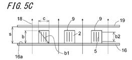
- FIG. 5C and 5D are schematic diagrams explaining the alignment method of this embodiment.
- a support member 16 made of a non-magnetic material and having a flat support surface 16a parallel to the horizontal direction, and a support member 16 made of a non-magnetic material and above the support member 16 A magnetic field in which magnetic flux lines 18 intersect the support surface 16a is applied to a plurality of base components 2 arranged in a gap with an upper member 19 provided at a predetermined distance from the support surface 16a, The directions of the base parts 2 are aligned.
- a magnetic field in which the magnetic flux lines 18 intersect the supporting surface 16a is applied to the plurality of element precursors 13 arranged in the gap between the support member 16 and the upper member 19. , the orientation of the element precursor 13 is aligned.
- the material constituting the support member 16 and the upper member 19 may be any non-magnetic material, such as resin material, hard paper, ceramic material, or non-magnetic metal material such as aluminum.
- the support member 16 and the upper member 19 may be made of any non-magnetic material, and may be made of a non-magnetic material having a thickness sufficient to provide rigidity so that it does not bend.
- the distance between the support member 16 and the upper member 19 is a distance that allows the base component 2 or the base body precursor 13 to rotate about the longitudinal direction, that is, the direction perpendicular to the end face 8 as the axial direction.
- the interval may be such that the element parts 2 (precursor elements 13) in the first state are not vertically overlapped with each other and the element elements 2 (precursor element 13) are prevented from being in the second state. .
- the vertical and horizontal dimensions of the end face 8 of the base component 2 are b and c, and the diagonal dimension of the end face 8 is b1.
- the distance s is set to b1 ⁇ s ⁇ (2 ⁇ b or a, whichever is smaller). good.
- Rotation of the base component 2 is allowed by setting b1 ⁇ s. By setting s ⁇ (2 ⁇ b or a, whichever is smaller), it is possible to prevent the overlapping of the base parts 2 in the first state and the transition to the second state.
- the width of the internal electrode layer 5 is b2
- the vertical and horizontal dimensions of the end face 8 of the element body precursor 13 are b2 and c
- the diagonal dimension of the end face 8 is b3.
- Rotation of the element precursor 13 is allowed by setting b3 ⁇ s.
- s ⁇ (2 ⁇ b2 or a, whichever is smaller) it is possible to inhibit the overlap of the element precursor 13 in the first state and the transition to the second state.
- the width b2 of the internal electrode layer 5 By setting the width b2 of the internal electrode layer 5 to 0.75b ⁇ b2 ⁇ b, the element component 2 can obtain a sufficient rotational moment by the action of the magnetic field even if it has the protective layer 6.
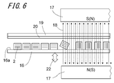
- FIG. 6 is a schematic diagram explaining an alignment method of another embodiment.
- the base component 2 placed in the gap between the support member 16 and the upper member 19 is relatively moved along the horizontal direction in the pre-generated magnetic field.
- the term "relative" as used herein means that the position of the magnetic field is fixed, and the base component 2 placed in the gap may be moved together with the support member 16 and the upper member 19, and the base component 2 placed in the gap may be moved. This means that the positions of the support member 16 and the upper member 19 may be fixed and the magnetic field generated in advance may be moved.
- the base component 2 spontaneously rotates so that the extending direction of the internal electrode layers 5 and the direction of the magnetic flux lines 18 are parallel to each other. The directions of the parts 2 can be aligned.
- the direction of rotation of the base component 2 can be made constant according to the direction of the magnetic flux lines 18 .
- the element body parts 2 are moved from the left side in a magnetic field with the magnetic flux lines 18 directed upward or downward, the element body parts 2 placed at the right end of the gap are all rotated clockwise to align their directions. Become. In this way, the direction of rotation of the base component 2 can be controlled.
- vibration may be imparted to the base component 2 placed in the gap between the support member 16 and the upper member 19 .
- vertical vibrations are applied as indicated by arrows 22 .
- vibration is applied to the support member 16 .
- the adjacent element parts 2 may hinder the rotation even if the magnetic field acts.
- the vibration direction is not limited to the vertical direction, but may be the horizontal direction, or a combination thereof.
- the magnetic field acting on the base component 2 may be generated by, for example, a magnet (first magnet) 17 positioned below the support member 16 and a magnet (second magnet) 17 positioned above the upper member 19 . Opposite sides of the two magnets 17 may have opposite polarities so that the magnetic flux lines 18 of the generated magnetic field intersect the support surface 16a.
- the magnet 17 may be a permanent magnet or an electromagnet.
- the size of the magnet 17 may be, for example, a magnet having an area larger than the area where the base component 2 is arranged on the support surface 16 a of the support member 16 .
- the magnetic field may, for example, be applied continuously to the base component 2, or an intermittent magnetic field may be used in which periods of application and periods of non-application are repeated.
- an intermittent magnetic field By using an intermittent magnetic field, it is possible to widen the distance between the element parts 2 in the same manner as in the case of applying the vibration described above.
- the magnet 17 is a permanent magnet
- the intermittent magnetic field has an active period during which it approaches the support member 16 and the upper member 19, and a non-active period during which it moves away from the support member 16 and the upper member 19. be able to.
- the magnet 17 is an electromagnet
- the period during which the current is supplied can be defined as the active period
- the period during which the current supply is stopped can be defined as the non-active period.
- the magnet 17 for example, only the magnet (first magnet) 17 positioned below the support member 16 may be used, or only the magnet (second magnet) 17 positioned above the upper member 19 may be used.
- a uniform magnetic field can be generated over a wide range.
- the base component 2 can be rotated and oriented at any position on the support surface 16a.
- the magnetic field may be a magnetic field in which the direction of the magnetic flux lines 18 (the direction of the magnetic field) is repeatedly reversed.
- the internal electrode layers 5 of the base component 2 are ferromagnetic, and when a magnetic field is applied to them, the internal electrode layers 5 are magnetized and may have residual magnetism. This residual magnetism may make it difficult to handle the base component 2 in subsequent processes. By repeatedly reversing the direction of the magnetic flux lines 18 , magnetization and demagnetization are repeated, and the residual magnetism of the internal electrode layers 5 can be reduced.
- FIG. 7 is a schematic diagram showing how a component assembly is formed.
- a plurality of element parts 2 aligned in the same direction are gathered under the action of a magnetic field to form a component.
- Form aggregates For example, the jig 25 is moved horizontally from the outside of the gap in the left-right direction toward the center.
- the base parts 2 sandwiched between the jigs 25 from both sides gather at the center to form an aggregate.
- a plurality of base parts 2 can be collectively processed by integrally handling the component assembly in the subsequent processing. As a result, it is possible to process the base parts 2 more quickly than when they are processed individually. Furthermore, it is possible to process a plurality of base parts 2 under the same conditions.
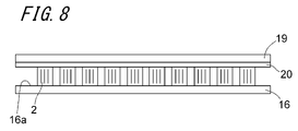
- FIG. 8 is a schematic diagram showing how the base component is fixed.
- the distance between the support member 16 and the upper member 19 is shortened while the magnetic field is applied.
- the action of the magnetic field is stopped in a state in which the plurality of base body parts 2 are held between the support member 16 and the upper member 19.
- the element body part 2 may rotate due to disturbance of the magnetic field at the time of stopping or subsequent handling, and the orientation may not be aligned.
- the base component 2 is fixed, and if the action of the magnetic field is stopped after that, the rotation of the base component 2 at the time of stopping can be prevented. can.
- the base component 2 When the base component 2 is sandwiched between the support member 16 and the upper member 19, the base component 2, the support member 16 and the upper member 19 come into contact with each other. At this time, a configuration may be used in which the portion of the upper member 19 facing the support surface 16a contains an elastic material so that the element component 2 will not be damaged even if an impact is applied to the element component 2 .
- the elastic sheet 20 may be attached to the upper member 19 .
- the elastic sheet 20 may be attached to the support member 16 in the same manner.
- the material of the elastic sheet 20 preferably has excellent durability and abrasion resistance, and for example, silicon rubber or urethane rubber can be used.
- the manufacturing method includes the alignment method described above.
- ceramic mixed powder obtained by adding an additive to BaTiO 3 which is a ceramic dielectric material is wet pulverized and mixed by a bead mill.
- a polyvinyl butyral-based binder, a plasticizer, and an organic solvent are added to and mixed with the pulverized and mixed slurry to prepare a ceramic slurry.
- a ceramic green sheet 10 is formed on the carrier film.
- the thickness of the ceramic green sheet 10 may be, for example, about 1 to 10 ⁇ m. As the thickness of the ceramic green sheet 10 is reduced, the capacitance of the laminated ceramic capacitor can be increased.
- the molding of the ceramic green sheets 10 is not limited to the die coater, and may be performed using, for example, a doctor blade coater or a gravure coater.
- a conductive paste containing nickel (Ni), which is a ferromagnetic metal material to be the internal electrode layers 5, is applied to the ceramic green sheets 10 prepared above by screen printing. pattern.
- the printing of the conductive paste is not limited to the screen printing method, and may be performed using, for example, the gravure printing method.
- the conductive paste may contain metals such as Pd, Cu, Ag, etc., or alloys thereof, in addition to Ni, for example.
- the pattern of the internal electrode layer 5 may be, for example, a pattern such as an individual electrode pattern.
- the internal electrode layer 5 after drying is in a state in which nickel particles are dispersed in the organic binder. As long as the characteristics as a capacitor can be secured, the thinner the internal electrode layer 5 is, the more the internal defects due to internal stress can be prevented. In the case of a capacitor with a high number of laminations, the thickness of the internal electrode layers 5 may be, for example, 2.0 ⁇ m or less.
- a predetermined number of ceramic green sheets 10 having internal electrode layers 5 printed thereon are laminated on the predetermined number of laminated ceramic green sheets 10, and then a predetermined number of ceramic green sheets 10 are laminated. do.
- a predetermined number of ceramic green sheets 10 on which the internal electrode layers 5 are printed are laminated while shifting the pattern of the internal electrode layers 5 .
- the ceramic green sheets 10 are laminated on a support sheet.
- the support sheet may be an adhesive release sheet such as a weak adhesive sheet or a foamed release sheet that can be adhered and peeled.
- a laminate formed by laminating a plurality of ceramic green sheets 10 is pressed in the lamination direction to obtain an integrated mother laminate 11 as shown in FIG.
- the laminate can be pressed using, for example, a hydrostatic press.
- Internal electrode layers 5 are buried in layers in the mother laminate 11 with the ceramic green sheets 10 interposed therebetween.
- the mother laminate 11 is cut lengthwise and crosswise, it becomes the element precursor 13 shown in FIG. Since the surfaces, end surfaces, and side surfaces of the mother laminate 11 correspond to the surface 7, the end surface 8, and the side surface 9, respectively, of the precursor body 13, they are given the same reference numerals below.
- a support sheet used when laminating the ceramic green sheets 10 is located under the mother laminate 11. As shown in FIG.
- the mother laminated body 11 is cut into predetermined dimensions using a press-cutting device to obtain a plurality of first rod-shaped bodies 12 .
- a cut surface of the first rod-shaped body 12 corresponds to the side surface 9 of the element precursor 13 , and the internal electrode layer 5 is exposed on the cut surface of the first rod-shaped body 12 .
- the method of cutting the mother laminated body 11 is not limited to the method using the press cutting device, and for example, a dicing saw device or the like may be used. All the internal electrode layers 5 have discontinuous portions divided at a plurality of locations in the longitudinal direction of the first rod-shaped body 12 .
- a discontinuous portion of the internal electrode layer 5 is, for example, 40 ⁇ m or more.
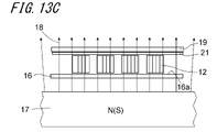
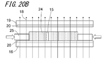
- FIG. 13A After arranging a plurality of first rod-shaped bodies 12 obtained by cutting on the support surface 16a of the support member 16, the upper member 19 is installed.
- the first rod-shaped bodies 12 are arranged so that their longitudinal directions are parallel to each other.
- the distance s between the support member 16 and the upper member 19 is, for example, 1.1 times the diagonal dimension b3 of the end face 8 of the first rod-shaped body 12 .
- FIG. 13B the support member 16 and the upper member 19 are moved to approach the magnet 17 so that the previously provided magnet 17 is positioned below the support member 16 .
- An electromagnet is used as the magnet 17 .
- the magnetic force is adjusted according to the distance from the magnet surface.
- the first rod-shaped body 12 to which the magnetic field of the magnet 17 is applied rotates around the axis extending in the longitudinal direction through the center of the end face 8 .
- all the first rod-shaped bodies 12 are aligned so that the extension direction of the internal electrode layers 5 is parallel to the magnetic flux lines 18 .
- the first rod-shaped bodies 12 aligned in the same direction are clamped and fixed between the upper member 19 and the support member 16 .
- the magnetic field acting on the first rod-shaped body 12, which is a laminated component can be controlled by the type of magnet used, the distance between the laminated component and the magnet, and so on.
- the magnetic flux density should be 50 gauss or more. , the type of magnet and the distance from the magnet.
- the action of the magnetic field on the first rod-shaped body 12 is stopped.
- the current supply to the magnet 17, which is an electromagnet may be stopped.
- an adhesive support sheet 21 is attached to the upper member 19, or another upper member to which the adhesive support sheet 21 is attached in advance.
- the upper member 19 with the support sheet 21 may be brought into contact with the aligned first rods 12 while the magnetic field is acting from above. .
- FIG. 13C shows that the upper member 19 with the support sheet 21 may be brought into contact with the aligned first rods 12 while the magnetic field is acting from above.
- the action of the magnetic field on the first rod 12 may be stopped by separating the first rod 12 from the magnet 17 while holding it between the upper member 19 and the support member 16 .
- the plurality of first rod-shaped bodies 12 fixed to the support sheet 21 can be moved while their directions are aligned.
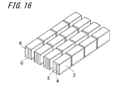
- FIG. 15 is a perspective view of the processed first rod-shaped body.
- the processing treatment is, for example, a treatment for forming the protective layer 6 .
- the ceramic slurry can be applied to the side surfaces 9 all at once with the side surfaces 9 of the first rods 12 oriented in the same direction. After drying, the side surface 9 coated with the ceramic slurry is fixed with another support sheet 21, and the original support sheet 21 is peeled off. The ceramic slurry is also applied to the side surface 9 newly exposed by peeling off the original support sheet 21 . By applying the ceramic slurry to the side surface 9 in this manner, the protective layer 6 can be formed.
- the ceramic slurry to be applied may have the same components as those of the ceramic green sheets 10 forming the mother laminate 11 .
- the base component 2 is obtained by cutting each first rod-shaped body 12 as shown in FIG. After firing the element component 2 thus obtained, the external electrodes 3 are formed, and the multilayer ceramic capacitor 1 can be manufactured.
- the firing temperature can be appropriately set according to the dielectric ceramic material and the metal material contained in the conductive paste forming the internal electrode layers 5 .
- the firing temperature may be, for example, 1100-1250°C.
- the mother laminated body 11 is cut into predetermined dimensions to obtain a plurality of second rod-shaped bodies 12A.
- the direction of cutting is 90° different from that of the first rod-shaped body 12 described above, and the cut surface of the second rod-shaped body 12A corresponds to the end surface 8 of the element precursor 13 .
- a thermoplastic resin 15 is embedded in the gaps between the second rods 12A obtained by cutting, and the surface (face) is covered with the thermoplastic resin 15 to obtain a flat block 23.
- the flat block 23 is further cut to obtain a third rod-like body 24, as shown in FIG.
- the cutting direction is 90° different from that of the second rod-shaped body 12A, and is the same as the cutting direction of the first rod-shaped body 12A.
- a cut surface of the third rod-shaped body 24 corresponds to the side surface 9 of the element precursor 13 .
- the third rod-shaped body 24 has a structure in which the precursor body 13 is connected with the thermoplastic resin 15 .
- the internal electrode layer 5 has discontinuous portions divided by the thermoplastic resin 15 at a plurality of locations in the longitudinal direction of the third rod-shaped body 24 . In such a case, since the apparent magnetic susceptibility of the internal electrode layers 5 in the longitudinal direction does not increase in the magnetic field, the third rod-like body 24 easily rotates about the longitudinal direction.
- a discontinuous portion of the internal electrode layer 5 is, for example, 40 ⁇ m or more.
- a method of aligning the direction of the third rod-shaped body 24 as a laminated part will be explained.
- the upper member 19 is installed.
- the respective first rod-shaped bodies 12 are arranged side by side so that their longitudinal directions are parallel.
- Both the support member 16 and the upper member 19 are attached with an elastic sheet 20 .
- two magnets 17 are arranged in advance, and the base component 2 placed in the gap between the support member 16 and the upper member 19 is positioned between the two magnets 17.
- the first rod-shaped body 12 is moved horizontally in a pre-generated magnetic field in a direction 90° to the longitudinal direction of the first rod-shaped body 12 .
- the third rod-shaped body 24 rotates spontaneously so that the extension direction of the internal electrode layer 5 and the direction of the magnetic flux line 18 are parallel, and the direction of the third rod-shaped body 24 can be aligned.
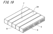
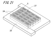
- a plurality of aligned third rod-shaped bodies 24 are assembled to form a component assembly 27 while a magnetic field is applied.
- the jig 25 is moved horizontally from the outside of the gap in the left-right direction toward the center.
- the jig 25 is an L-shaped formwork, and the two jigs 25 position the plurality of third rods 24 in the longitudinal direction and in the direction perpendicular to the longitudinal direction.
- a plate-like component assembly 27 is formed.
- the parts assembly 27 and the jig 25 are fixed with the support sheet 21 provided on the upper member 19 .
- the side surface 9 of the base body precursor 13 is exposed on the opposite side of the part assembly 27 fixed by the support sheet 21 .
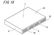
- FIG. 22 is a schematic diagram showing how a component assembly is processed.
- the processing treatment is, for example, a treatment of polishing the side surface 9 .
- a polishing disk 28 can be used to polish the exposed side surface 9 of the part assembly 27 fixed by the support sheet 21 .
- Polishing is performed using a plurality of whetstones and polishing powders, proceeding from coarse grit to fine grit.
- abrasive grains with an average grain size of 1 ⁇ m or less may be used, and abrasive grains with an average grain size of 0.5 ⁇ m or less may be used.
- the abrasive grain material may be diamond abrasive grains that are excellent in polishability and do not easily react with the dielectric material and the electrode material during firing.
- the polished side surface 9 is fixed with another support sheet 21, and the original support sheet 21 is peeled off.
- the side surface 9 of the assembly of parts 27 newly exposed by peeling off the original support sheet 21 can also be polished.
- FIG. 23 is a perspective view showing another example of the upper member.
- a plate-like member similar to the support member 16 is used as the upper member 19 .
- the upper member 19 only needs to be able to define a plurality of laminated parts so that they are not oriented vertically and two parts do not overlap, for example a mesh member or a vertical grid. It may be a member.
- the upper member 19A in the illustrated example is a vertical grid member. In the case of a vertical grid member, the upper member 19A may be arranged so that the vertical grid is non-parallel to the longitudinal direction of the laminated component.
- a method for aligning laminated parts of the present disclosure includes: a support member made of a non-magnetic material and having a horizontally parallel and flat support surface; A rectangular parallelepiped laminated component in which a plurality of ceramic green sheets and ferromagnetic electrode layers are alternately laminated in a space defined by an upper member provided at a predetermined distance from the surface. , exert a magnetic field whose magnetic flux lines intersect said support surface to align the laminate components.
- the manufacturing method of the laminated ceramic component of the present disclosure includes the method of aligning the laminated components described above, and after processing the surfaces of the laminated components aligned in the same direction, the laminated components are fired.
- the orientation of laminated components can be easily and quickly aligned simply by placing a plurality of laminated components on a flat support surface.
- the laminated ceramic component can be manufactured easily and quickly.
- each embodiment is not limited to that embodiment, and may be used in combination. Further, for example, a ceramic green sheet serving as a protective layer or a plate-like assembly provided with ceramic slurry may be cut before firing, or the plate-like assembly may be washed after polishing. Thus, changing the processing conditions of each embodiment or adding a new step to each embodiment does not affect the gist of the present disclosure.
Landscapes
- Engineering & Computer Science (AREA)
- Power Engineering (AREA)
- Manufacturing & Machinery (AREA)
- Microelectronics & Electronic Packaging (AREA)
- Ceramic Engineering (AREA)
- Chemical & Material Sciences (AREA)
- Inorganic Chemistry (AREA)
- Fixed Capacitors And Capacitor Manufacturing Machines (AREA)
- Ceramic Capacitors (AREA)
Abstract
Description
、保護層6を有していても、磁界の作用によって十分な回転モーメントが得られる。
体部品2に対して同一条件で加工することができる。
体部品2を固定し、その後に磁界の作用を停止すれば、停止時の素体部品2の回転を防ぐことができる。
2 素体部品
3 外部電極
4 誘電体セラミックス
5 内部電極層
6 保護層
7 面
8 端面
8A 第1の端面
8B 第2の端面
9 側面
10 セラミックグリーンシート
11 母積層体
12 第一棒状体
12A 第二棒状体
13 素体前駆体
15 熱可塑性樹脂
16 支持部材
16a 支持面
17 磁石
18 磁束線
19、19A 上方部材
20 弾性シート
21 支持シート
22 矢印
23 平板状ブロック
24 第三棒状体
25 冶具
27 部品集合体
28 研磨盤
35 誘電体セラミック粒子
36 ニッケル粒子
Claims (13)
- 非磁性体材料を含み、水平方向に平行で平坦な支持面を有する支持部材と、非磁性体材料を含み、前記支持部材の上方であって、前記支持面から所定の距離を隔てた位置に有する上方部材との間隙に複数配置された、セラミックグリーンシートと強磁性体層とが交互に積層された直方体形状の積層部品に、磁束線が前記支持面と交差する磁界を作用させて、積層部品の向きを揃える、積層部品の整列方法。
- 前記間隙に配置された積層部品に振動を付与する、請求項1記載の積層部品の整列方法。
- 前記磁界が、間欠性の磁界である、請求項1または2記載の積層部品の整列方法。
- 前記磁界が、磁束線の向きが繰り返し反転する磁界である、請求項1~3のいずれか1つに記載の積層部品の整列方法。
- 前記支持部材の下方に位置する第1磁石と前記上方部材の上方に位置する第2磁石とによって前記磁界を発生させる、請求項1~4のいずれか1つに記載の積層部品の整列方法。
- 前記間隙に配置された積層部品を予め発生している磁界中に移動させる、請求項1~5のいずれか1つに記載の積層部品の整列方法。
- 前記間隙に、積層部品に磁界が作用した状態で、向きが揃った複数の積層部品を集合させて部品集合体を形成する、請求項1~6のいずれか1つに記載の積層部品の整列方法。
- 向きが揃った複数の積層部品を前記支持部材と前記上方部材とによって挟持した状態で、磁界の作用を停止する、請求項1~7のいずれか1つに記載の積層部品の整列方法。
- 前記上方部材の、前記支持面に対向する部分が弾性材料を含む、請求項1~8のいずれか1つに記載の積層部品の整列方法。
- 前記上方部材は、網状部材または縦格子状部材である、請求項1~9のいずれか1つに記載の積層部品の整列方法。
- 前記強磁性体層は、強磁性金属材料と有機バインダとを含み、有機バインダの含有量が、体積比率で強磁性金属材料の1.5倍以下である、請求項1~10のいずれか1つに記載の積層部品の整列方法。
- 前記強磁性体層は、積層部品の長手方向において不連続部分を有する、請求項1~11のいずれか1つに記載の積層部品の整列方法。
- 請求項1~12のいずれか1つに記載の積層部品の整列方法を含み、
向きが揃った積層部品の表面に加工処理を行ったのち、積層部品を焼成する、積層セラミック部品の製造方法。
Priority Applications (4)
| Application Number | Priority Date | Filing Date | Title |
|---|---|---|---|
| US18/279,912 US20240145182A1 (en) | 2021-03-02 | 2022-03-01 | Method for aligning multilayer components and method for manufacturing multilayer ceramic electronic components |
| JP2023503857A JPWO2022186190A1 (ja) | 2021-03-02 | 2022-03-01 | |
| CN202280018751.9A CN116997982A (zh) | 2021-03-02 | 2022-03-01 | 层叠部件的排列方法以及层叠陶瓷电子部件的制造方法 |
| KR1020237029827A KR20230138004A (ko) | 2021-03-02 | 2022-03-01 | 적층 부품의 정렬 방법 및 적층 세라믹 전자 부품의 제조 방법 |
Applications Claiming Priority (2)
| Application Number | Priority Date | Filing Date | Title |
|---|---|---|---|
| JP2021-032935 | 2021-03-02 | ||
| JP2021032935 | 2021-03-02 |
Publications (1)
| Publication Number | Publication Date |
|---|---|
| WO2022186190A1 true WO2022186190A1 (ja) | 2022-09-09 |
Family
ID=83154742
Family Applications (1)
| Application Number | Title | Priority Date | Filing Date |
|---|---|---|---|
| PCT/JP2022/008563 WO2022186190A1 (ja) | 2021-03-02 | 2022-03-01 | 積層部品の整列方法および積層セラミック電子部品の製造方法 |
Country Status (5)
| Country | Link |
|---|---|
| US (1) | US20240145182A1 (ja) |
| JP (1) | JPWO2022186190A1 (ja) |
| KR (1) | KR20230138004A (ja) |
| CN (1) | CN116997982A (ja) |
| WO (1) | WO2022186190A1 (ja) |
Citations (8)
| Publication number | Priority date | Publication date | Assignee | Title |
|---|---|---|---|---|
| JPH10284355A (ja) * | 1997-04-09 | 1998-10-23 | Murata Mfg Co Ltd | 電子部品の整列装置及び整列方法 |
| JP2001150249A (ja) * | 1999-11-26 | 2001-06-05 | Matsushita Electric Ind Co Ltd | 電子部品の整列方法および整列装置並びに電子部品の製造方法 |
| JP2011018698A (ja) * | 2009-07-07 | 2011-01-27 | Murata Mfg Co Ltd | 電子部品搬送装置 |
| JP2012134498A (ja) * | 2010-12-21 | 2012-07-12 | Samsung Electro-Mechanics Co Ltd | 積層セラミックキャパシタの回路基板実装構造、方法及び回路基板のランドパターン、積層セラミックキャパシタの包装体並びに整列方法 |
| JP2015084406A (ja) * | 2013-09-20 | 2015-04-30 | 株式会社村田製作所 | コンデンサ素子の製造方法および製造装置 |
| JP2019175902A (ja) * | 2018-03-27 | 2019-10-10 | 太陽誘電株式会社 | チップ部品の整列方法及び磁石 |
| JP2020017764A (ja) * | 2015-09-10 | 2020-01-30 | 株式会社村田製作所 | 電子部品の搬送装置 |
| JP2020141085A (ja) * | 2019-03-01 | 2020-09-03 | 太陽誘電株式会社 | セラミックチップ部品の処理方法、積層セラミック電子部品の製造方法及び積層セラミック電子部品包装体の製造方法 |
Family Cites Families (1)
| Publication number | Priority date | Publication date | Assignee | Title |
|---|---|---|---|---|
| JP3653630B2 (ja) | 2001-06-25 | 2005-06-02 | Tdk株式会社 | チップ部品の向き整列方法 |
-
2022
- 2022-03-01 KR KR1020237029827A patent/KR20230138004A/ko unknown
- 2022-03-01 CN CN202280018751.9A patent/CN116997982A/zh active Pending
- 2022-03-01 US US18/279,912 patent/US20240145182A1/en active Pending
- 2022-03-01 WO PCT/JP2022/008563 patent/WO2022186190A1/ja active Application Filing
- 2022-03-01 JP JP2023503857A patent/JPWO2022186190A1/ja active Pending
Patent Citations (8)
| Publication number | Priority date | Publication date | Assignee | Title |
|---|---|---|---|---|
| JPH10284355A (ja) * | 1997-04-09 | 1998-10-23 | Murata Mfg Co Ltd | 電子部品の整列装置及び整列方法 |
| JP2001150249A (ja) * | 1999-11-26 | 2001-06-05 | Matsushita Electric Ind Co Ltd | 電子部品の整列方法および整列装置並びに電子部品の製造方法 |
| JP2011018698A (ja) * | 2009-07-07 | 2011-01-27 | Murata Mfg Co Ltd | 電子部品搬送装置 |
| JP2012134498A (ja) * | 2010-12-21 | 2012-07-12 | Samsung Electro-Mechanics Co Ltd | 積層セラミックキャパシタの回路基板実装構造、方法及び回路基板のランドパターン、積層セラミックキャパシタの包装体並びに整列方法 |
| JP2015084406A (ja) * | 2013-09-20 | 2015-04-30 | 株式会社村田製作所 | コンデンサ素子の製造方法および製造装置 |
| JP2020017764A (ja) * | 2015-09-10 | 2020-01-30 | 株式会社村田製作所 | 電子部品の搬送装置 |
| JP2019175902A (ja) * | 2018-03-27 | 2019-10-10 | 太陽誘電株式会社 | チップ部品の整列方法及び磁石 |
| JP2020141085A (ja) * | 2019-03-01 | 2020-09-03 | 太陽誘電株式会社 | セラミックチップ部品の処理方法、積層セラミック電子部品の製造方法及び積層セラミック電子部品包装体の製造方法 |
Also Published As
| Publication number | Publication date |
|---|---|
| KR20230138004A (ko) | 2023-10-05 |
| CN116997982A (zh) | 2023-11-03 |
| US20240145182A1 (en) | 2024-05-02 |
| JPWO2022186190A1 (ja) | 2022-09-09 |
Similar Documents
| Publication | Publication Date | Title |
|---|---|---|
| US8410887B2 (en) | Built-in-coil substrate | |
| US9865395B2 (en) | Method and device for manufacturing capacitor element | |
| KR101462757B1 (ko) | 적층 세라믹 커패시터, 그 제조방법 및 적층 세라믹 커패시터가 내장된 인쇄회로기판 | |
| JP6131756B2 (ja) | コンデンサ素子の製造方法 | |
| JPS5927520B2 (ja) | 圧電性セラミックス多層素子及びその製造方法 | |
| KR20170077034A (ko) | 적층 세라믹 전자 부품 및 그 제조 방법 | |
| KR101462758B1 (ko) | 적층 세라믹 커패시터, 그 제조방법 및 적층 세라믹 커패시터가 내장된 인쇄회로기판 | |
| JP2000082852A (ja) | 多層圧電アクチュエ―タおよびその製造方法 | |
| JP7319792B2 (ja) | セラミックチップ部品の処理方法、積層セラミック電子部品の製造方法及び積層セラミック電子部品包装体の製造方法 | |
| WO2022186190A1 (ja) | 積層部品の整列方法および積層セラミック電子部品の製造方法 | |
| JP7116470B2 (ja) | チップ部品の整列方法 | |
| JP3931631B2 (ja) | 電子部品チップの取扱方法および電子部品チップの整列装置 | |
| JP7127720B2 (ja) | 積層セラミック電子部品の製造方法 | |
| CN112185706B (zh) | 一种多层陶瓷电容器的制造方法及多层陶瓷电容器 | |
| WO2023032591A1 (ja) | 積層部品の整列方法およびその整列方法を用いた積層セラミック電子部品の製造方法 | |
| JPH07235442A (ja) | 積層セラミック電子部品の製造方法 | |
| TWI840898B (zh) | 積層陶瓷電子零件及其製造方法 | |
| WO2022224828A1 (ja) | 切断方法および積層セラミック部品の製造方法 | |
| JP4450148B2 (ja) | 導電ペーストの付与方法及び積層セラミック電子部品の製造方法 | |
| CN112071642B (zh) | 一种多层陶瓷电容器的制备方法 | |
| JPH04145674A (ja) | 電歪効果素子及びその製造方法 | |
| KR100819555B1 (ko) | 압전 공진자를 가지는 압전 공진 장치의 형성방법들 | |
| WO2022181260A1 (ja) | 積層セラミック電子部品の製造方法 | |
| KR101922872B1 (ko) | 연마 장치 | |
| CN117642831A (zh) | 层叠陶瓷电子部件及其制造方法 |
Legal Events
| Date | Code | Title | Description |
|---|---|---|---|
| 121 | Ep: the epo has been informed by wipo that ep was designated in this application |
Ref document number: 22763245 Country of ref document: EP Kind code of ref document: A1 |
|
| ENP | Entry into the national phase |
Ref document number: 20237029827 Country of ref document: KR Kind code of ref document: A |
|
| WWE | Wipo information: entry into national phase |
Ref document number: 18279912 Country of ref document: US Ref document number: 202280018751.9 Country of ref document: CN Ref document number: 1020237029827 Country of ref document: KR Ref document number: 2023503857 Country of ref document: JP |
|
| NENP | Non-entry into the national phase |
Ref country code: DE |
|
| 122 | Ep: pct application non-entry in european phase |
Ref document number: 22763245 Country of ref document: EP Kind code of ref document: A1 |