WO2022180722A1 - 画像読取装置 - Google Patents
画像読取装置 Download PDFInfo
- Publication number
- WO2022180722A1 WO2022180722A1 PCT/JP2021/007003 JP2021007003W WO2022180722A1 WO 2022180722 A1 WO2022180722 A1 WO 2022180722A1 JP 2021007003 W JP2021007003 W JP 2021007003W WO 2022180722 A1 WO2022180722 A1 WO 2022180722A1
- Authority
- WO
- WIPO (PCT)
- Prior art keywords
- light
- light receiving
- shielding member
- image reading
- light shielding
- Prior art date
- Legal status (The legal status is an assumption and is not a legal conclusion. Google has not performed a legal analysis and makes no representation as to the accuracy of the status listed.)
- Ceased
Links
Images








Classifications
-
- H—ELECTRICITY
- H04—ELECTRIC COMMUNICATION TECHNIQUE
- H04N—PICTORIAL COMMUNICATION, e.g. TELEVISION
- H04N1/00—Scanning, transmission or reproduction of documents or the like, e.g. facsimile transmission; Details thereof
- H04N1/024—Details of scanning heads ; Means for illuminating the original
- H04N1/028—Details of scanning heads ; Means for illuminating the original for picture information pick-up
- H04N1/03—Details of scanning heads ; Means for illuminating the original for picture information pick-up with photodetectors arranged in a substantially linear array
- H04N1/031—Details of scanning heads ; Means for illuminating the original for picture information pick-up with photodetectors arranged in a substantially linear array the photodetectors having a one-to-one and optically positive correspondence with the scanned picture elements, e.g. linear contact sensors
- H04N1/0311—Details of scanning heads ; Means for illuminating the original for picture information pick-up with photodetectors arranged in a substantially linear array the photodetectors having a one-to-one and optically positive correspondence with the scanned picture elements, e.g. linear contact sensors using an array of elements to project the scanned image elements onto the photodetectors
-
- H—ELECTRICITY
- H10—SEMICONDUCTOR DEVICES; ELECTRIC SOLID-STATE DEVICES NOT OTHERWISE PROVIDED FOR
- H10F—INORGANIC SEMICONDUCTOR DEVICES SENSITIVE TO INFRARED RADIATION, LIGHT, ELECTROMAGNETIC RADIATION OF SHORTER WAVELENGTH OR CORPUSCULAR RADIATION
- H10F39/00—Integrated devices, or assemblies of multiple devices, comprising at least one element covered by group H10F30/00, e.g. radiation detectors comprising photodiode arrays
- H10F39/80—Constructional details of image sensors
- H10F39/806—Optical elements or arrangements associated with the image sensors
- H10F39/8063—Microlenses
-
- H—ELECTRICITY
- H04—ELECTRIC COMMUNICATION TECHNIQUE
- H04N—PICTORIAL COMMUNICATION, e.g. TELEVISION
- H04N1/00—Scanning, transmission or reproduction of documents or the like, e.g. facsimile transmission; Details thereof
- H04N1/024—Details of scanning heads ; Means for illuminating the original
- H04N1/028—Details of scanning heads ; Means for illuminating the original for picture information pick-up
- H04N1/02815—Means for illuminating the original, not specific to a particular type of pick-up head
- H04N1/0282—Using a single or a few point light sources, e.g. a laser diode
- H04N1/02835—Using a single or a few point light sources, e.g. a laser diode in combination with a light guide, e.g. optical fibre, glass plate
-
- H—ELECTRICITY
- H04—ELECTRIC COMMUNICATION TECHNIQUE
- H04N—PICTORIAL COMMUNICATION, e.g. TELEVISION
- H04N1/00—Scanning, transmission or reproduction of documents or the like, e.g. facsimile transmission; Details thereof
- H04N1/024—Details of scanning heads ; Means for illuminating the original
- H04N1/028—Details of scanning heads ; Means for illuminating the original for picture information pick-up
- H04N1/02815—Means for illuminating the original, not specific to a particular type of pick-up head
- H04N1/02895—Additional elements in the illumination means or cooperating with the illumination means, e.g. filters
-
- H—ELECTRICITY
- H04—ELECTRIC COMMUNICATION TECHNIQUE
- H04N—PICTORIAL COMMUNICATION, e.g. TELEVISION
- H04N1/00—Scanning, transmission or reproduction of documents or the like, e.g. facsimile transmission; Details thereof
- H04N1/024—Details of scanning heads ; Means for illuminating the original
- H04N1/028—Details of scanning heads ; Means for illuminating the original for picture information pick-up
- H04N1/03—Details of scanning heads ; Means for illuminating the original for picture information pick-up with photodetectors arranged in a substantially linear array
- H04N1/0306—Details of scanning heads ; Means for illuminating the original for picture information pick-up with photodetectors arranged in a substantially linear array using a plurality of optical elements arrayed in the main scan direction, e.g. an array of lenses
Definitions
- the present disclosure relates to an image reading device.
- An image reading device that acquires two-dimensional image information by optically reading an object to be imaged (hereinafter also referred to as "subject"). See, for example, US Pat.
- the image reading device of Patent Document 1 includes a light shielding member including a plurality of light receiving portions that are regularly arranged, a plurality of openings that are arranged corresponding to the plurality of light receiving portions, and light shielding members corresponding to the plurality of openings, respectively. and an array of microlenses.
- each light-receiving unit includes a plurality of light-receiving pixels arranged in the X-axis direction and the Y-axis direction on the XY plane. This improves resolution.
- an imaging optical system is configured by one light-receiving pixel, an aperture corresponding to the light-receiving pixel, and a microlens corresponding to the aperture.
- An object of the present disclosure is to increase the depth of field while improving the resolution.
- An image reading device is an image reading device that optically reads an object to be imaged, and includes a plurality of light receiving units that are regularly arranged and corresponding to the plurality of light receiving units. a first light shielding member including a plurality of first openings arranged in the same manner as the above; and a plurality of microlenses arranged corresponding to the plurality of first openings, wherein the plurality of light receiving units includes a plurality of light-receiving pixels arranged in a first direction that is the main scanning direction, and each microlens of the plurality of microlenses is object-side telecentric, reflects off the object, and the plurality of microlenses so that the light passing through the microlenses and the first openings corresponding to the microlenses is incident on the plurality of light receiving pixels included in the light receiving section corresponding to the first openings; , the first light shielding member, and the plurality of light receiving portions are arranged.
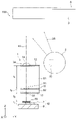
- FIG. 1 is a perspective view schematically showing a main configuration of an image reading device according to Embodiment 1;
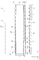
- FIG. 2 is a cross-sectional view of the image reading device shown in FIG. 1 taken along line A2-A2;
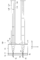
- FIG. 2 is a cross-sectional view of the image reading device shown in FIG. 1 taken along line A3-A3;
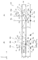
- FIG. 4 is a plan view showing a part of the configuration of the imaging device unit shown in FIGS. 1 to 3;
- FIG. 5A is a plan view showing a configuration of a light receiving pixel unit arranged closest to an end portion in the +X-axis direction of the sensor chip among the plurality of light receiving pixel units shown in FIG. 4;
- FIG. 1 is a perspective view schematically showing a main configuration of an image reading device according to Embodiment 1;
- FIG. 2 is a cross-sectional view of the image reading device shown in FIG. 1 taken along line A2-A2;
- FIG. 2 is a cross-sectional view
- FIG. 5B is a plan view showing the configuration of a light-receiving pixel unit arranged closest to the end of the sensor chip in the ⁇ X-axis direction among the plurality of light-receiving pixel units shown in FIG. 4;
- FIG. 5C is a plan view showing a configuration of a light receiving pixel unit other than the light receiving pixel units shown in FIGS. 5A and 5B among the plurality of light receiving pixel units shown in FIG. 4;
- FIG. 2 is a diagram schematically showing the configuration of an illumination optical section shown in FIG. 1 and illumination light emitted from the illumination optical section;
- FIG. (A) is a plan view showing two light-receiving pixel units positioned in the same column.
- FIG. 4 is a diagram showing imaging rays of reflected light incident on each of the two light-receiving pixel units shown in FIG. 7(A).
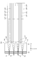
- 4 is a diagram showing a part of the configuration of the image reading device shown in FIG. 3 and principal rays in the image reading device;
- FIG. 4 is a diagram showing principal rays incident on light-receiving pixel units positioned in a first row and principal rays incident on light-receiving pixel units positioned in a second row in the image reading device according to Embodiment 1.
- FIG. 4 is a diagram showing part of the configuration of the image reading device shown in FIG. 3 and reflected light passing through a first opening and a second opening;
- FIG. 10 is a diagram showing backlight rays directed in the +Z-axis direction from light-receiving pixel units in the image reading device according to Embodiment 1;
- FIG. 10 is a diagram showing backlight rays directed in the +Z-axis direction from light-receiving pixel units in the image reading device according to Embodiment 1;
- FIG. 8 is a diagram showing the tilt of the optical axis of the microlens when the first glass member and the second glass member are misaligned in the image reading device according to the first embodiment;
- FIG. 10 is a diagram showing the positions of the fields of view of the microlenses in the X-axis direction when there is variation in the mounting of the sensor chips in the image reading device according to the comparative example;
- FIG. 7 is a cross-sectional view schematically showing the main configuration of an image reading device according to Embodiment 2;
- FIG. 11 is a cross-sectional view schematically showing a main configuration of an image reading device according to a modification of Embodiment 2;
- FIG. 11 is a plan view showing the configuration of an imaging element unit of an image reading apparatus according to Embodiment 3;
- FIG. 11 is a plan view showing the configuration of an imaging element unit of an image reading apparatus according to Embodiment 4;
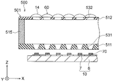
- FIG. 12 is a cross-sectional view schematically showing the main configuration of an image reading device according to Embodiment 5;
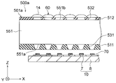
- FIG. 14 is a cross-sectional view schematically showing the main configuration of an image reading device according to Modification 1 of Embodiment 5;
- FIG. 12 is a cross-sectional view schematically showing a main configuration of an image reading device according to Modification 2 of Embodiment 5;
- FIG. 12 is a cross-sectional view schematically showing the main configuration of an image reading device according to Embodiment 6;
- FIG. 1 is a perspective view schematically showing the main configuration of an image reading apparatus 100 according to Embodiment 1.
- FIG. FIG. 2 is a cross-sectional view of the image reading apparatus 100 shown in FIG. 1 taken along line A2-A2.
- FIG. 3 is a cross-sectional view of the image reading apparatus 100 shown in FIG. 1 taken along line A3-A3.
- the image reader 100 includes an imaging optical section 1, an illumination optical section 2, and a top plate glass 3 as a document table.
- the illumination light 25 is scattered and reflected by the document 6 .
- the scattered reflected light (hereinafter also referred to as “reflected light”) is received by the imaging optical unit 1, whereby the image information of the document 6 is read.
- the image reading device 100 is an image reading device that optically reads the document 6 .
- the document 6 in order for the imaging optical unit 1 to acquire two-dimensional image information of the document 6, the document 6 is moved along the top plate glass 3 by the conveying unit (not shown) as the first direction.
- the sheet is conveyed in the sub-scanning direction, which is the second direction orthogonal to the main scanning direction.
- the main scanning direction is the X-axis direction
- the sub-scanning direction is the Y-axis direction.
- the entire document 6 may be scanned by moving the imaging optical unit 1 in the Y-axis direction while the document 6 remains stationary.
- the manuscript 6 is an example of an object to be imaged by the imaging optical unit 1 .
- the manuscript 6 is, for example, a printed material on which characters, images, or the like are printed.
- the document 6 is placed on a predetermined reference plane S. As shown in FIG.
- the reference surface S is a plane on which the document 6 is placed, specifically, a surface on the top plate glass 3 .
- Top plate glass 3 is positioned between document 6 and imaging optical unit 1 .
- the thickness of the top plate glass 3 is, for example, 1.0 mm. Note that the structure for setting the document 6 on the reference surface S is not limited to the top plate glass 3 .
- the imaging optical section 1 includes an imaging element unit 10 as an imaging section, a first light shielding member 11 including a plurality of apertures 31, a second light shielding member 12 including a plurality of apertures 32, and a plurality of apertures 33. It has a third light shielding member 13 and a plurality of microlenses 14 .
- FIG. 4 is a plan view showing a part of the configuration of the imaging element unit 10 shown in FIGS. 1-3.
- the imaging element unit 10 has a plurality of sensor chips 7a, 7b, 7c, a sensor substrate 8, and an image processing device 9.
- FIG. A plurality of sensor chips 7a, 7b, 7c are arranged in the X-axis direction.
- the sensor chips 7a, 7b, and 7c are collectively referred to as "sensor chip 7" when there is no need to distinguish between the sensor chips 7a, 7b, and 7c.
- the sensor chip 7 is made of silicon material, for example.
- a sensor chip 7 is provided on a sensor substrate 8 .
- the sensor chip 7 is electrically connected to the sensor substrate 8 by wire bonding, for example.
- the sensor substrate 8 is a mounting substrate and is made of, for example, glass epoxy resin.
- the image processing device 9 executes image processing based on the image signal output from the sensor chip 7 .
- the image processing device 9 is, for example, an ASIC (Application Specific Integrated Circuit) mounted on the sensor substrate 8 .
- the image processing device 9 can also be realized by an arithmetic processing device that is not mounted on the sensor substrate 8 . Details of the image processing performed by the image processing device 9 will be described later.
- a plurality of light-receiving pixel units 70 as a plurality of light-receiving portions arranged regularly are arranged in one sensor chip 7 .
- a plurality of light-receiving pixel units 70 are arranged in the X-axis direction.
- One sensor chip 7 has, for example, 64 light receiving pixel units 70 .
- Each light-receiving pixel unit 70 receives reflected light reflected by the document 6 .
- one sensor chip 7 is not limited to the configuration described in the first embodiment, and can be realized by a set of any number of light-receiving pixel units 70 .
- the plurality of light-receiving pixel units 70 includes a plurality of light-receiving pixel units 71 arranged at different positions in the Y-axis direction in a first row 70m and a plurality of light-receiving pixels arranged in a second row 70n. and unit 72 .
- a center position interval (hereinafter also referred to as “pitch”) P between two light receiving pixel units 71 (or two light receiving pixel units 72) adjacent to each other in the X-axis direction is, for example, 320 ⁇ m.
- the interval q between the center positions of the light receiving pixel units 71 and 72 adjacent to each other in the Y-axis direction is, for example, 400 ⁇ m.
- the light-receiving pixel unit 72 in the second column 70n is located between the two light-receiving pixel units 71 in the first column 70m.
- the light-receiving pixel units 72 are arranged in the X-axis direction at a pitch P/2, which is half the pitch P (hereinafter also referred to as “pitch P 0 ”), with respect to the light-receiving pixel units 71 belonging to different columns. arranged staggered.
- the plurality of light-receiving pixel units 70 are arranged in a zigzag pattern.
- the pitch P can be increased compared to a configuration in which a plurality of light-receiving pixel units are arranged in a row. can be obtained.
- the aperture can be made larger, the brightness of the image becomes brighter.
- a plurality of light-receiving pixel units 70 included in one sensor chip 7 includes light-receiving pixel units 70z and 70a as first light-receiving portions and second light-receiving portions as light-receiving portions other than the light-receiving pixel units 70z and 70a. and a light receiving pixel unit 70x.
- the light-receiving pixel unit 70z is a light-receiving pixel unit arranged at a position closest to the end 7e of the sensor chip 7 in the +X-axis direction.
- the light-receiving pixel unit 70a is a light-receiving pixel unit arranged closest to the end 7f of the sensor chip 7 in the -X-axis direction.
- FIG. 5A is a plan view showing the configuration of the light receiving pixel unit 70z.
- FIG. 5B is a plan view showing the configuration of the light receiving pixel unit 70a.
- the light-receiving pixel units 70z and 70a each include a plurality of light-receiving pixels 80.
- one light-receiving pixel 80 has a square shape of 10 ⁇ m ⁇ 10 ⁇ m, for example.
- each of the light receiving pixel units 70z and 70a has a rectangular shape of 50 ⁇ m ⁇ 30 ⁇ m, for example. Further, when the interval between the X-axis direction center positions of the light receiving pixels 80 adjacent to each other in the X-axis direction is defined as P1, the interval P1 is 10 ⁇ m.
- FIG. 5(C) is a plan view showing the configuration of the light receiving pixel unit 70x.
- the light-receiving pixel unit 70x in the light-receiving pixel unit 70x, four light-receiving pixels 80 are arranged in the X-axis direction and three light-receiving pixels 80 are arranged in the Y-axis direction. Therefore, one light-receiving pixel unit 70x has, for example, a rectangular shape of 40 ⁇ m ⁇ 30 ⁇ m.
- the number of light-receiving pixels 80 included in the light-receiving pixel units 70z, 70a, and 70x is not limited to the configurations shown in FIGS. Further, the arrangement method of the light receiving pixels 80 in the light receiving pixel units 70z, 70x, and 70a is not limited to the matrix, and may be another arrangement method.
- the number of light-receiving pixels 80 included in the light-receiving pixel units 70z and 70a is greater than the number of light-receiving pixels 80 included in the light-receiving pixel unit 70x.
- the number of light-receiving pixels 80 included in the light-receiving pixel units 70z and 70a may be the same as the number of light-receiving pixels 80 included in the light-receiving pixel unit 70x. That is, the number of the plurality of light receiving pixels 80 included in the light receiving pixel units 70z and 70a should be equal to or greater than the number of the plurality of light receiving pixels 80 included in the light receiving pixel unit 70b.
- Points C 1 , C 2 , and C 3 shown in FIGS. 5A to 5C respectively correspond to the optical axis 40 of the microlens 14 (see FIG. 2, for example) and the light receiving pixel units 70z, 70a, and 70z. It is the intersection with 70x.
- a point C3 shown in FIG. 5C coincides with the center position of the light receiving pixel unit 70x.
- Each light receiving pixel 80 of the plurality of light receiving pixels 80 has a color filter (not shown).
- the light-receiving pixel unit 70 includes a first light-receiving pixel 80R having a red filter that transmits red light, a second light-receiving pixel 80G having a green filter that transmits green light, and a light-receiving pixel 80G having a green filter that transmits green light. and a third light-receiving pixel 80B having a blue filter that transmits the .
- illumination light for example, illumination light 25 shown in FIG. 6 to be described later
- the light-receiving pixel unit 70 can also be realized by a plurality of light-receiving pixels 80 that do not have color filters.
- the first light shielding member 11 is arranged closer to the document 6 than the light receiving pixel unit 70 is.
- the first light shielding member 11 includes a plurality of openings 31 as a plurality of first openings.
- the plurality of openings 31 are arranged at positions corresponding to the plurality of light receiving pixel units 70 respectively. When viewed in the Z-axis direction, the multiple apertures 31 overlap the multiple light-receiving pixel units 70 . Specifically, the center position of each of the plurality of openings 31 is the same as the center position of the light receiving pixel unit 70 on the XY plane.
- the plurality of openings 31 are arranged in two rows.
- the openings 31 in each row are arranged in the X-axis direction.
- the plurality of openings 31 are arranged in a zigzag pattern.
- the opening 31 is, for example, a square of 40 ⁇ m ⁇ 40 ⁇ m. Reflected light reflected by the document 6 passes through the opening 31 .
- the portion other than the opening 31 is the first light shielding portion 41 that shields the reflected light.
- the second light shielding member 12 is arranged closer to the document 6 than the first light shielding member 11 is.
- the second light shielding member 12 is arranged between the first light shielding member 11 and the plurality of microlenses 14 .
- the second light shielding member 12 includes a plurality of openings 32 as a plurality of second openings.
- the plurality of apertures 32 are arranged at positions corresponding to the plurality of microlenses 14 respectively. Specifically, the central position of each of the plurality of openings 32 is the same as the central position of the microlens 14 on the XY plane. When viewed in the Z-axis direction, the multiple apertures 32 overlap the multiple light-receiving pixel units 70 .
- the plurality of openings 32 are arranged in two rows.
- the openings 32 in each row are arranged in the X-axis direction.
- a plurality of openings 32 are arranged in a zigzag pattern.
- the plurality of openings 32 respectively overlap the plurality of openings 31 and also overlap the plurality of openings 33 to be described later.
- the opening 32 is circular, for example.
- the opening area of the opening 32 is larger than the opening areas of the openings 31 and 33 . That is, the diameter of the opening 32 (diameter ⁇ shown in FIG. 13 to be described later) is larger than each side of the openings 31 and 33 .
- the diameter of the opening 32 is, for example, 280 ⁇ m. Reflected light reflected by the document 6 passes through the opening 32 .
- the portion other than the opening 32 is the second light shielding portion 42 that shields the reflected light.
- the imaging optical section 1 further has a glass member 51 as a first translucent member arranged between the first light shielding member 11 and the second light shielding member 12 .
- the first light shielding member 11 is formed on the surface 51a of the glass member 51 on the ⁇ Z axis side (that is, the light receiving pixel unit 70 side), and is formed on the surface 51b of the glass member 51 on the +Z axis side (that is, the original 6 side).
- a second light shielding member 12 is formed.
- the first light shielding member 11 and the second light shielding member 12 are thin light shielding layers formed of a chromium oxide film deposited on the glass member 51 .
- the openings 31 and 32 are formed by etching the chromium oxide film using a mask pattern. Thereby, the positional accuracy and shape accuracy of the openings 31 and 32 can be improved. For example, the positional error in the Y-axis direction between the plurality of openings 31 (or between the plurality of openings 32) is approximately 1 ⁇ m.
- the third light shielding member 13 is arranged closer to the light receiving pixel unit 70 than the first light shielding member 11 is.
- the third light shielding member 13 includes a plurality of openings 33 as a plurality of third openings.
- the plurality of openings 33 are arranged at positions corresponding to the plurality of light receiving pixel units 70 respectively.
- the multiple apertures 33 overlap the multiple light-receiving pixel units 70 .
- the center position of each aperture 33 of the plurality of apertures 33 is the same as the center position of the light receiving pixel unit 70 .
- the plurality of openings 33 are arranged in two rows.
- the openings 33 in each row are arranged in the X-axis direction.
- the plurality of openings 33 are arranged in a zigzag pattern.
- the opening 33 has, for example, a square shape of 60 ⁇ m ⁇ 60 ⁇ m. Reflected light reflected by the document 6 passes through the aperture 33 .
- the portion other than the opening 33 is the third light shielding member 13 that shields the reflected light.
- the imaging optical section 1 further has a glass member 52 as a second translucent member arranged between the first light shielding member 11 and the third light shielding member 13 .
- the glass member 52 is arranged closer to the light receiving pixel unit 70 than the glass member 51 is.
- a third light shielding member 13 is formed on the surface 52a of the glass member 52 on the ⁇ Z axis side (that is, on the light receiving pixel unit 70 side).
- a method of forming the opening 33 is the same as the method of forming the openings 31 and 32 described above, and is formed by etching a chromium oxide film deposited on the glass member 52, for example. Note that the imaging optical unit 1 can be realized without the second light shielding member 12, the third light shielding member 13, and the glass member 52, as shown in FIG. 16, which will be described later.
- the glass member 52 is fixed by being adhered to the glass member 51 with an adhesive or the like so that the center position of the opening 33 overlaps the center position of the opening 31 and the center position of the opening 32. It is In order to improve the accuracy of alignment when bonding the glass member 52 to the glass member 51, the +Z-axis side surface of the glass member 52 and the -Z-axis side surface 51b of the glass member 51 are aligned. may be provided with alignment marks (not shown) for
- the glass members 51 and 52 are members capable of transmitting light, and are, for example, glass substrates.
- the refractive index of glass member 51 is the same as the refractive index of glass member 52 .
- a refractive index n of the glass members 51 and 52 is, for example, 1.52.
- the wire when the above-described wire bonding is used as a method of electrically connecting the sensor chip 7 and the sensor substrate 8, the wire is about 100 to 200 ⁇ m in the +Z-axis direction from the +Z-axis side surface of the sensor chip 7. It can jump out.
- the distance t 0 (see FIG. 2) between the light receiving pixel unit 70 and the glass member 52 is 500 ⁇ m, which is longer than the length of the wire. can be prevented from interfering with
- a spacer member (not shown) having a thickness greater than 500 ⁇ m (specifically, the total value of the distance t0 and the distance t7 shown in FIG. 2) is provided between the sensor substrate 8 and the glass. It is arranged between the member 52 .
- an interval t0 of 500 ⁇ m is accurately ensured.
- the interval t7 is the distance from the +z-axis side surface of the sensor substrate 8 to the +z-axis side surface of the light receiving pixel unit 70 .
- the multiple microlenses 14 are arranged on the +Z-axis side of the multiple openings 32 .
- the optical axis of microlens 14 is indicated by reference numeral 40 (see FIGS. 2 and 3).
- the microlenses 14 are spaced apart from the plurality of apertures 31 in the optical axis direction (that is, the Z-axis direction) via the glass member 51 .
- the microlens 14 is a condensing lens that condenses the light reflected by the document 6 .
- the microlens 14 is, for example, a convex lens.
- the plurality of microlenses 14 are arranged at positions corresponding to the plurality of light receiving pixel units 70 respectively.
- the plurality of microlenses 14 overlap the plurality of light receiving pixel units 70 when viewed in the Z-axis direction.
- the plurality of microlenses 14 are arranged in two rows. Each row of microlenses 14 is arranged in the X-axis direction.
- the plurality of microlenses 14 are arranged in a zigzag pattern.
- the microlenses 14 arranged in a zigzag form constitute a microlens array 60 .
- the microlens array 60 is manufactured, for example, by a method such as nanoimprinting or injection molding.
- the mold used to manufacture the microlens array 60 has recesses corresponding to the shape of the microlens array 60 .
- the nanoimprinting method allows the microlens array 60 to be directly formed on the second light shielding member 12 .
- the diameter of the microlens 14 is set to a predetermined size within the range of several ⁇ m to several mm.
- the radius of curvature of the surface of the microlens 14 is, for example, approximately 1.0 mm.
- the plurality of microlenses 14 are arranged at positions respectively corresponding to the plurality of openings 31 . Specifically, the center position of the microlens 14 overlaps the center position of the aperture 31 on the XY plane. Thereby, the optical axis 40 of the microlens 14 extends in the Z-axis direction perpendicular to the XY plane.
- FIG. 6 is a diagram schematically showing the configuration of the illumination optical section 2 shown in FIG. 1 and the illumination light 25 emitted from the illumination optical section 2.
- the illumination optical section 2 has a light source 20 and a light guide 21 .
- the light source 20 is arranged on the end surface 21 a of the light guide 21 .
- the light source 20 emits light 20 a inside the light guide 21 .
- the light source 20 is, for example, a semiconductor light source.
- the semiconductor light source is, for example, an LED (Light Emitting Diode).
- the light guide 21 directs the light 20a emitted from the light source 20 to the manuscript 6.
- the light guide 21 is, for example, a cylindrical member made of translucent resin material.
- Light 20 a emitted from the light source 20 propagates while repeating total reflection inside the light guide 21 .
- a scattering region 22 is formed in a partial region of the inner surface of the light guide 21 .
- the light 20a is scattered when it hits the scattering region 22, and the light 20a becomes scattered light. A part of the scattered light becomes illumination light 25 that illuminates the document 6 .
- the illumination light 25 applied to the manuscript 6 shown in FIG. 2 is reflected by the manuscript 6 and becomes reflected light.
- the reflected light passes through the microlens 14 , the opening 32 , the glass member 51 , the opening 31 , the glass member 52 and the opening 33 in order and enters the light receiving pixel unit 70 .
- FIG. 7A is a plan view showing two light receiving pixel units 70 positioned in the same column.
- FIG. 7B is a diagram showing imaging rays L11 to L14 of reflected light incident on each of the two light-receiving pixel units 70 shown in FIG. 7A.
- the imaging light beams L11 to L14 are directed in the opposite direction (that is, the +Z-axis direction) from the center position of each of the four second light receiving pixels 80G among the plurality of light receiving pixels 80 included in one light receiving pixel unit 70. It's a back ray.
- the microlens 14 forms an image of the document 6 positioned on the object plane onto the light receiving pixel units 70 positioned on the imaging plane.
- the reduction ratio between the object plane and the imaging plane (hereinafter also referred to as "image transfer magnification") is 1/4.
- the interval P 1 (see FIG. 5A) between the center positions of the light-receiving pixels 80 adjacent in the X-axis direction is 10 ⁇ m.
- the number of light receiving pixels 80 arranged in the X-axis direction is four.
- the resolution of the image reading device 100 on the document 6 in the X-axis direction (in other words, the pitch of the conjugate image of the light-receiving pixels 80 on the document 6) is r
- the resolution r is 40 ⁇ m.
- one microlens 14, one aperture 32, one aperture 31, one aperture 33, and one light-receiving pixel unit 70 constitute an imaging unit 110, which is a unit optical system. be done.
- a plurality of light receiving pixel units 70 are formed on one sensor chip 7 . Therefore, the positional accuracy between the plurality of light receiving pixel units 70 can be improved. Therefore, there is little variation in the position of the optical axis 40 of the microlens 14 between the imaging units 110 adjacent in the X-axis direction.
- the aperture 31 determines the respective numerical apertures on the imaging side and the object side. If the opening width of the opening 31 is large, the numerical aperture on the object side is large, so that the amount of light reflected by the document 6 can be increased. However, in this case, the depth of field is reduced.
- an image affected by stray light may be obtained.
- an image that is not affected by stray light is obtained by satisfying Conditions 1 and 2, which will be described later.
- the microlens 14 is object-side telecentric. Thereby, the depth of field can be increased.
- the aperture 33 which is the diaphragm surface of the microlens 14 , is arranged at the rear focal point of the microlens 14 .
- FIG. 8 is a diagram showing principal rays L21 to L24 in the image reading device 100 according to Embodiment 1.
- the principal rays L21 to L24 are rays passing through the center of the aperture 33 among the imaging rays L11 to L14 shown in FIG. 7B.
- the centers of the apertures 31, 32, and 33 overlap when viewed in the Z-axis direction. straight line passing through the center) are parallel along the Z-axis direction.
- the principal rays L21 to L24 of each microlens 14 are parallel along the optical axis direction.
- principal rays L21 to L24 of imaging rays L11 to L14 reflected by an object (specifically, the document 6) and formed into an image in the imaging optical section 1 are parallel to each other along the Z-axis direction. .
- the distances in the X-axis direction between the principal rays L21 to L24 on the object side do not change, and the reduction ratio does not change.
- the distance between the light receiving pixel unit 70 and the third light shielding member 13 is t 0
- the distance between the third light shielding member 13 and the first light shielding member 11 is denoted as t2
- the distance between the first light shielding member 11 and the second light shielding member 12 is denoted by t1
- the refractive index of each of the glass members 51 and 52 is denoted by n.
- the reflected light that has been reflected by the document 6 and has passed through the microlens 14 and the opening 31 corresponding to the microlens 14 is incident on the plurality of light receiving pixels 80 included in the light receiving pixel unit 70 corresponding to the opening 31 .
- a plurality of microlenses 14, a first light shielding member 11, and a plurality of light receiving pixel units 70 are arranged.
- the position of the document 6 in the Z-axis direction is about 8 mm away from the position of the microlens 14 in the Z-axis direction on the +Z-axis side (see FIG. 1). That is, in Embodiment 1, the object distance is approximately 8 mm. Therefore, the illumination optical unit 2 and the top plate glass 3 can be arranged between the document 6 and the microlens 14 .
- the depth of field is determined by the numerical aperture of the microlens 14 on the object side.
- the numerical aperture on the object side is determined by the width of the aperture 31 and the interval t0 . That is, a desired depth of field can be obtained by changing the aperture width of the aperture 31 .
- the definition of the depth of field changes depending on the allowable range of image contrast, in the first embodiment, the depth of field is approximately 8 mm. You can get depth of field.
- the aperture 33 is the diaphragm surface of the microlens 14 in Embodiment 1, the aperture 31 may be the diaphragm surface. At this time, if the aperture 31 is arranged at the position of the back focal point of the microlens 14, object-side telecentricity can be realized.
- the number N of light-receiving pixels 80 arranged in the X-axis direction included in one light-receiving pixel unit 70 is equal to or greater than a predetermined number. need to be As shown in FIG. 4 described above, in the plurality of light-receiving pixel units 70 arranged in two staggered rows, the pitch P0 between two adjacent light-receiving pixel units 71 and 72 is P/ 2 .
- the distance between the center positions of two microlenses 14 adjacent to each other in the X-axis direction is also P/2.
- the pitch P0 is equal to the width of the microlens 14 in the X-axis direction, which is the visual field range of one microlens 14 . Therefore, it is possible to prevent image information from being lost between the two microlenses 14 .
- the formula (2) is satisfied, overlapping of the fields of view of adjacent microlenses 14 can also be prevented.
- FIG. 9 shows principal rays L21 to L24 incident on the light-receiving pixel units 71 located in the first row 70m shown in FIG.
- FIG. 10 is a diagram showing chief rays L31 to L34 incident on a light receiving pixel unit 72.
- FIG. 9 and FIG. 12 described later the microlens 14 overlapping the light receiving pixel unit 71 is called a microlens 141, and the microlens 14 overlapping the light receiving pixel unit 72 is called a microlens 142.
- FIG. 9 and FIG. 12 described later, the microlens 14 overlapping the light receiving pixel unit 71 is called a microlens 141, and the microlens 14 overlapping the light receiving pixel unit 72 is called a microlens 142.
- the distance in the X-axis direction between the optical axis of the microlens 141 and the optical axis of the microlens 142 is 160 ⁇ m. Therefore, in the space on the object side, the four principal rays L21 to L24 are arranged at intervals of 40 ⁇ m in the X-axis direction. The four principal rays L21 to L24 are also arranged at intervals of 40 ⁇ m in the X-axis direction. That is, the spatial resolution in the X-axis direction on the object side is 40 ⁇ m, and the spatial resolution between the imaging units 110 adjacent in the X-axis direction is 40 ⁇ m and does not change.
- Embodiment 1 all the principal rays L21 to L24 and L31 to L34 are parallel to the Z-axis direction. Therefore, the reduction ratio does not change regardless of the position of the document 6 in the Z-axis direction. Therefore, between the imaging units 110 belonging to different columns, it is possible to prevent the lack of image information, and it is also possible to prevent overlapping of fields of view.
- FIG. 10 is a diagram showing part of the configuration of the image reading apparatus 100 shown in FIG. 3 and reflected light passing through the openings 31 and 33. As shown in FIG. FIG. 10 describes conditions for acquiring an image that is not affected by stray light traveling in the X-axis direction.
- the plurality of light-receiving pixel units 70 arranged in the X-axis direction are also denoted as 70a, 70b, and 70c.
- the plurality of openings 31 are also denoted as 31a, 31b, and 31c
- the plurality of openings 33 are denoted as 33a, 33b, and 33c.
- straight lines connecting the center of the aperture 32, the center of the aperture 31, and the light receiving pixel unit 70 are referred to as optical axes 40a, 40b, and 40c.
- reflected light from the document 6 (see FIG. 1) passing through the openings 31 and 33 is shown as light rays L1, L2, and L3.
- the light beam L1 enters the light receiving pixel unit 70a through the openings 31a and 33a.
- FIG. 11A and 11B are diagrams for explaining the conditions under which the reflected light that has passed through the openings 31 and 33 is incident on the light receiving pixel unit 70 in the image reading device 100.
- the thickness of the glass member 52 is denoted by t 2
- the refractive index of the glass member 52 by n 2
- the distance between the glass member 52 and the light receiving pixel unit 70 by t 0 .
- Condition 1 is a sufficient condition that the smallest incident angle .theta..sub.1 at the aperture 31 among the rays passing through the apertures 31 and 33 having optical axes different from each other satisfies the following equation (3). n 2 ⁇ sin ⁇ 1 >1 (3)
- Expression (3) is expressed using the parameters of the thickness of the glass member 52 and the opening width.
- the half widths of the openings 31 and 33 which are half the widths of the openings, are denoted by X 1 and X 3 , respectively.
- a half width of the width of the light-receiving pixel unit 70 in the X-axis direction is expressed as X0 .
- the distance D1 in the X-axis direction between the ⁇ X-axis direction end in the opening 33w and the +X-axis direction end in the opening 33v is obtained by the following equation (4).
- D 1 (P/2) - X 1 - X 2 (4)
- Equation (6) is derived from equations (3) and ( 5 ) for the thickness t2 of the glass member 52 that satisfies condition 1 above. That is, if the thickness t2 of the glass member 52 is thinner than the value on the right side of Equation (6), the light ray L4 satisfies the total internal reflection condition. At this time, condition 1 is satisfied.
- one light-receiving pixel unit 70b of the plurality of light-receiving pixel units 70 and light-receiving pixel units 70a and 70c adjacent to the light-receiving pixel unit 70b on both sides in the X-axis direction will be described as an example.
- a light ray L6 passing through a point P5 in the opening 31b overlapping with the light receiving pixel unit 70b and a point P6 in the opening 33b overlapping with the light receiving pixel unit 70b reaches the area between the light receiving pixel unit 70a and the light receiving pixel unit 70c.
- condition 2 is satisfied.
- the region between the light-receiving pixel unit 70a and the light-receiving pixel unit 70c is the region sandwiched between the right end of the light-receiving pixel unit 70a and the left end of the light-receiving pixel unit 70c shown in FIG. 11B.
- a light ray L6 shown in FIG. 11B is a light ray that passes through the opening 31b and the opening 33b that overlaps it.
- the light ray L6 passes through the end of the aperture 31b closest to the aperture 31c and then through the end of the aperture 33b closest to the aperture 33a.
- a light ray L6 that has passed through the aperture 33b reaches the point Q0.
- a point Q0 indicates a point at which the light beam L6 reaches the region between the light receiving pixel units 70a and 70b.
- the point Q0 indicates the point farthest from the light-receiving pixel unit 70b in the ⁇ X-axis direction, that is, the point closest to the light-receiving pixel unit 70a.
- the light ray L6 passes through the openings 31b and 33b.
- the light rays do not reach openings other than the light-receiving pixel unit 70b (for example, the light-receiving pixel unit 70a and the light-receiving pixel unit 70c).
- the incident angle ⁇ 2 is obtained by the following equation (7).
- tan ⁇ 2 (X 1 +X 2 )/t 2 (7)
- the relationship between the output angle ⁇ 1 and the incident angle ⁇ 2 is given by the following equation ( 8 ).
- n 2 ⁇ sin ⁇ 2 sin ⁇ 1 (8)
- the distance D2 from the optical axis 40b to the point Q0 is obtained by the following equation ( 9).
- D 2 X 1 +t 0 ⁇ tan ⁇ 1 (9)
- the condition that the point Q0 is located closer to the light receiving pixel unit 70b side than the end of the light receiving pixel unit 70a in the +X-axis direction is expressed by the following equation (10).
- Equation (11) is derived from equations (7) to (10). That is, when the thickness t2 of the glass member 52 is thicker than the value on the right side of Equation (11), Condition 2 above is established.
- X 1 20 ⁇ m
- X 2 30 ⁇ m
- X 0 20 ⁇ m
- t 0 500 ⁇ m
- P/2 160 ⁇ m
- n 2 1.52.
- the plurality of light receiving pixel units 70 are arranged in multiple rows and multiple columns.
- the plurality of light-receiving pixel units 70 are arranged in a zigzag pattern.
- the main scanning direction (that is, the X-axis direction) is
- the array pitch of the light-receiving pixel units should be half the array pitch of the light-receiving pixel units 70 of the first embodiment (that is, 160 ⁇ m). In other words, in the image reading device 100 according to Embodiment 1, the arrangement pitch of the light receiving pixel units 70 arranged in the same row can be increased.
- the thickness t2 that satisfies both the above-described formulas (6) and (11) is set while increasing the value of the half width of each opening. hard to get. Note that even when a plurality of light-receiving pixel units are arranged in one row , there exists a thickness t2 that is a parameter that satisfies both equations (6) and (11).
- the description excluding the description of the configuration in which the plurality of light-receiving pixel units 70 are arranged in two rows is that the plurality of light-receiving pixel units 70 are arranged in one row. Applies even when arrayed.
- FIG. 12 is a cross-sectional view of the image reading device 100 shown in FIG. 1 taken along line A12-A12.
- the openings 31 and 33 overlapping the light receiving pixel unit 71 are denoted by 311 and 331
- the openings 31 and 33 overlapping the light receiving pixel unit 72 are denoted by 312 and 332.
- the optical axis of the microlens 141 is indicated by 40a
- the optical axis of the microlens 142 is indicated by 40e.
- a point R1 is the edge of the light-receiving pixel unit 71 closest to the light-receiving pixel unit 72 .
- Point R2 is the edge of opening 332 closest to opening 331 .
- a point R3 is a point located outside the end of the opening 312 farthest from the opening 311 .
- a reverse light ray L8 which is a virtual light ray directed from the light receiving pixel unit 71 toward the opening 312, is used.
- the reverse ray L8 is a ray that passes from the point R1 to the point R2 and reaches the point R3.
- the distance between the point R3 and the optical axis 40e is denoted by D3
- the length of half the diagonal length of the square opening 312 is denoted by X20 .
- the back ray L 8 reaches the first shaded portion 41 .
- the backlight L8 passes through the opening 312
- the backlight L8 reaches the second light blocking portion 42 if the interval q shown in FIG. 4 is large. . Therefore, even if the distance D3 is smaller than the length X20 , the light rays passing through the openings 312 and 332 are It does not enter the light-receiving pixel unit 71 .
- FIG. 13 is a diagram showing backlight rays 61b, 62b, 63b, and 66b directed in the +Z-axis direction from the light-receiving pixel unit 70b in the image reading device 100.
- FIG. 13 the glass member 51 with a refractive index of n and a thickness of t 1 is illustrated as the glass member 51 with a refractive index of 1 and a thickness of t 1 /n, that is, as a glass member replaced with air.
- a glass member 52 having a refractive index of n and a thickness of t 2 is illustrated as a glass member 52 having a refractive index of 1 and a thickness of t 2 /n.
- the microlens 14 is spaced apart from the opening 32b of the second light shielding member 12 by a distance t 2 /n.
- the backlights 61b, 62b, 63b, and 66b are backlights directed in the +Z-axis direction from the object plane of the light receiving surface of the light receiving pixel unit 70b.
- the opening width (diameter ⁇ in FIG. 13) of the opening 32 of the second light shielding member 12 is smaller than the outer diameter of the microlens 14 . Therefore, the backlight 66b shown in FIG. 13 reaches the second light shielding portion 42. As shown in FIG. Since the backlight 66b is a backlight directed in the +Z-axis direction from the end of the light-receiving pixel unit 70b in the -X-axis direction, all the light rays incident on the light-receiving pixel unit 70b pass through the opening 32b.
- the image reading apparatus 100 can read an image with good image quality.
- the reading width of the image reading apparatus 100 ⁇ Relationship between reading width and number of sensor chips>
- the relationship between the reading width (hereinafter also referred to as "reading length") of the image reading apparatus 100 and the number of sensor chips 7 will be described.
- the image sensor unit 10 has a plurality of sensor chips 7 arranged in the X-axis direction, thereby realizing an image reading device 100 with a reading length of 200 mm.
- the specific number of sensor chips 7 will be described below.
- the pitch P of the light-receiving pixel units 70 described above is expressed by the following equation (12) using the number N of the light-receiving pixels 80 arranged in the X-axis direction in one light-receiving pixel unit 70 and the resolution r.
- P 2Nr (12)
- the imaging range A is expressed by the following equation (13) based on the number M and the resolution r.
- A M ⁇ r (13)
- FIG. 7 In order to prevent such defects, for example, a light receiving pixel unit 70z positioned at the +X-axis direction end of the sensor chip 7a shown in FIG. The distance from the unit 70a must be P/2 (160 ⁇ m in the first embodiment).
- the distance from the point C1 on the light-receiving pixel unit 70z to the +X-axis direction end 70e of the light - receiving pixel unit 70z, and the point C on the light-receiving pixel unit 70a 2 to the edge 70f of the light-receiving pixel unit 70a in the -X - axis direction is called a distance P2.
- the distance between the light receiving pixel unit 70z and the light receiving pixel unit 70a shown in FIG. 4 is Xg
- the distance Xg is expressed by the following formula (14).
- Xg P/2 ⁇ 2 ⁇ P 2 (14)
- a single sensor chip 7 is formed by cutting a silicon wafer with a dicing machine. Therefore, a margin is required when cutting a silicon wafer in consideration of a cutting allowance or a cutting error.
- the distance between the +X-axis direction end 70e of the light-receiving pixel unit 70z and the +X-axis direction end 7e of the sensor chip 7a, and the ⁇ X-axis direction end 70f of the light-receiving pixel unit 70a and the end of the sensor chip 7a in the ⁇ X-axis direction is set to a value smaller than 60 ⁇ m, which is 1/2 of the above-mentioned interval Xg. Thereby, pixel defects can be prevented in the boundary area between the adjacent sensor chips 7 . Since the image transfer magnification of the microlens 14 is 1/4, which is smaller than 1, a margin necessary for cutting the silicon wafer can be provided.
- Embodiment 1 ⁇ Relationship between assembly error and acquired image> As described above, in Embodiment 1, multiple openings are formed on the same glass member, and multiple microlenses 14 are also formed on the same glass member 51 . Thereby, it is possible to improve the positional accuracy between the plurality of apertures or the plurality of microlenses 14 located on the same plane.
- the first light shielding member 11 including a plurality of openings 31 the second light shielding member 12 including a plurality of openings 32, and the microlens array 60 including a plurality of microlenses 14 are formed on the glass member 51. formed.
- the third light shielding member 13 including the plurality of openings 33 is formed on the glass member 52 .
- the positioning accuracy between the center position of the microlens 14 and the center positions of the openings 31, 32, and 33 and the position in the Z-axis direction can be improved. It is conceivable to improve the accuracy of the positioning of the center positions of the openings 31, 32, and 33 having different .
- alignment of members whose positions in the Z-axis direction are different from each other tends to have a larger error than alignment of members located on the same plane.
- a step of bonding the glass member 51 and the glass member 52 using alignment marks is required, it is difficult to reduce the error to zero.
- 14A and 14B are diagrams illustrating the inclination of the optical axis of the microlens when the first glass member and the second glass member are misaligned in the image reading device according to the first embodiment.
- the center positions of the glass members 51 and 52 are deviated from the center position of the imaging device unit 10 toward the +X-axis side. Further, the center position of the glass member 51 in the X-axis direction is shifted to the +X-axis side with respect to the center position of the glass member 52 in the X-axis direction.
- the optical axis of the microlens 14 when such positional deviation occurs is denoted by reference numeral 45.
- An optical axis 45 of the microlens 14 is inclined with respect to the optical axis 40 toward the +X-axis side. Therefore, the intersection point where the optical axis 45 and the light-receiving pixel unit 70 intersect (for example, point C 3 shown in FIG. 5C) is shifted in the ⁇ X-axis direction.
- the center position of the image sensor unit 10 in the X-axis direction is aligned with the center position of the glass members 51 and 52 in the X-axis direction so that the crossing point matches the center position of the light-receiving pixel unit 70 in the X-axis direction. Alignment work is required to adjust the
- Embodiment 1 although the glass members 51 and 52 are shifted in the X-axis direction with respect to the imaging element unit 10, the optical axes 45 adjacent to each other in the X-axis direction are parallel to each other. . This prevents the fields of view of the microlenses 14 from overlapping or separating from each other between adjacent imaging units 110 (see FIG. 7B). Therefore, even when the glass members 51 and 52 are misaligned with respect to the image sensor unit 10, the image reading apparatus 100 can read an image having good image quality without duplication or loss of image information.
- the center positions of the microlenses 14 and the apertures 31, 32, and 33 in one imaging unit 110 may vary. occurs.
- adjacent optical axes 45 are not parallel to each other as in the first embodiment.
- the fields of view of the microlenses 14 overlap or are separated between adjacent imaging units 110, resulting in duplication or lack of image information. Therefore, in the image reading apparatus 100 having a plurality of imaging units 110, the plurality of microlenses 14 are integrally formed in the same plane and the plurality of openings are integrally formed in the same plane. , is a configuration necessary for reading an image with good image quality.
- FIG. 15 is a diagram showing the position of the field of view of the microlens 14 in the X-axis direction when the sensor chips 7a and 7b are mounted differently in the image reading device 101 according to the comparative example.
- the number of light receiving pixels 80 arranged in the X-axis direction in the light receiving pixel units 70aa and 70za arranged closest to the ends in the X-axis direction of the sensor chips 7a and 7b is four. This is different from the image reading apparatus 100 according to the first embodiment in this point.
- the field of view imaged on the sensor chip 7a is denoted by reference numeral 91
- the field of view imaged on the sensor chip 7b is denoted by reference numeral 92.
- the regions arranged in the X-axis direction by dividing the field of view 91 are denoted by reference numerals 91a, 91b, and 91c
- the regions arranged in the X-axis direction by dividing the field of view 92 are denoted by reference numerals 91a, 91b, and 91c.
- Reference numerals 92a, 92b, and 92c are used.
- the sensor chip 7a is shifted by 10 ⁇ m corresponding to one pixel of the light receiving pixel 80 in the +X-axis direction.
- the sensor chip 7b is shifted by 10 ⁇ m in the ⁇ X-axis direction.
- the visual field 91 shifts in the ⁇ X-axis direction by 40 ⁇ m corresponding to one pixel, and a visual field defect area 93 is generated.
- the visual field 92 shifts by 40 ⁇ m in the +X-axis direction, resulting in a visual field defect area 94 . Therefore, a field defect of 80 ⁇ m corresponding to two pixels is generated between the field of view 91 and the field of view 92 .
- the visual field defect area 93 forms an image on an area 95 adjacent to the light-receiving pixel unit 70za in the -X-axis direction. Also, the visual field defect region 94 forms an image on a region 96 adjacent to the light receiving pixel unit 70aa in the +X-axis direction.
- the number of light-receiving pixels 80 arranged in the X-axis direction in light-receiving pixel units 70z and 70a is the same as that in light-receiving pixel unit 70b in the X-axis direction. is larger than the number of light-receiving pixels 80 arranged in a row.
- the light-receiving pixels 80 are arranged in the visual field defect regions 93 and 94 . As a result, even if the mounting of the sensor chips 7a and 7b varies, it is possible to prevent the loss of the field of view.
- correction is performed by image processing. be able to. This correction method will be described later.
- the image processing device 9 converts the analog image signal output from the sensor chip 7 into digital image data, and executes the following image processing.
- the plurality of light-receiving pixel units 70 are arranged in a zigzag pattern. is shifted in the Y-axis direction by a distance q from the center position of the light-receiving pixel unit 72 belonging to . Therefore, when the document 6 is scanned in the Y-axis direction, it is necessary to restore an image without positional deviation.
- image processing device 9 acquires the image information from the light receiving pixel units 71 on the first row 70m and the image information from the light receiving pixel units 72 on the second row 70n.
- image combining process A process of shifting the number of pixels corresponding to the distance q and image information (hereinafter referred to as "image combining process") is performed.
- the light-receiving pixel units 70 in the second row 70n are arranged with a pitch P/2 that is half the pitch P in the X-axis direction with respect to the light-receiving pixel units 70 in the first row 70m.
- the image processing device 9 scans the light-receiving pixel unit 70 at a time interval when the document 6 is conveyed in the Y-axis direction by the resolution r on the document surface.
- the distance q indicating the positional deviation amount of the image information is preferably an integral multiple of the resolution r on the document surface, but is not limited to this.
- the image processing device 9 may estimate the brightness value of the sub-pixel position using the pixel interpolation process, and synthesize the image information using the estimated brightness value.
- the image processing device 9 shifts the timing at which the light-receiving pixel units 71 belonging to the first column 70m acquire the image information and the timing at which the light-receiving pixel units 72 belonging to the second column 70n acquire the image information. You may synthesize
- one light-receiving pixel 80 is additionally arranged in the X-axis direction in the light-receiving pixel units 70z and 70a arranged closest to the end of the sensor chip 7 in the X-axis direction. . Therefore, even if the mounting of the sensor chip 7 varies in the X-axis direction within the range of the single light receiving pixel 80, no light receiving pixel is lost in the document 6.
- FIG. 1 A block diagrammatic representation
- the field of view 91z overlaps the field of view 91a.
- the image information acquired by the sensor chip 7a and the image information acquired by the sensor chip 7b are combined in the image processing device 9, processing for removing overlapping light-receiving pixels may be performed.
- image interpolation processing is performed at sub-pixel positions so as not to cause contradiction between the overlapping fields of view 91, and the image is restored. Just do it.
- the interval between the reading positions on the document 6 between the sensor chips 7 adjacent in the X-axis direction deviates from the distance q in the Y-axis direction.
- this deviation is corrected based on the shift amount, which is the distance by which the image processing device 9 shifts the image information in the Y-axis direction.
- the sub-pixel deviation in the Y-axis direction can be corrected by performing image interpolation processing at the sub-pixel position.
- the image reading device 100 has a plurality of light-receiving pixel units 70 that are regularly arranged.
- Each light-receiving pixel unit 70 includes a plurality of light-receiving pixels 80 arranged in the main scanning direction.
- the resolution can be improved in the image reading apparatus 100 .
- the microlens 14 is telecentric on the object side. Further, the light reflected by the document 6 and passing through the microlens 14 and the opening 31 corresponding to the microlens 14 is incident on the plurality of light receiving pixels 80 included in the light receiving pixel unit 70 corresponding to the opening 31. A plurality of microlenses 14, a first light shielding member 11, and a plurality of light receiving pixel units 70 are arranged. Therefore, the field of view of the microlens 14 does not overlap with the field of view of another adjacent microlens 14, and there is no gap. As a result, the depth of field is increased, so that the distance between the position of the document 6 in the Z-axis direction and the position of the microlens 14 in the Z-axis direction, which is the imaging position on the object side, can be increased.
- the plurality of light receiving pixel units 70 are arranged in a zigzag manner, and the plurality of openings 31 are arranged in a zigzag manner so as to correspond to the plurality of light receiving pixel units 70 respectively.
- a plurality of microlenses 14 are arranged in a zigzag pattern so as to correspond to the plurality of openings 31 respectively.
- the pitch P0 between the light-receiving pixel units 71 and the light-receiving pixel units 72 belonging to different columns among the plurality of light-receiving pixel units 70 satisfies the formula ( 2 ) described above.
- the depth of field can be increased in the image reading apparatus 100 .
- the image reading device 100 includes the surface 51a provided with the first light shielding member 11 including the plurality of openings 31 and the microlens array 60 (that is, the plurality of microlenses 14). and a glass member 51 including a curved surface 51b.
- the first light shielding member 11 and the microlens array 60 can be integrally formed on the same member.
- the positional accuracy of the plurality of apertures 31 and the plurality of microlenses 14 can be enhanced. Therefore, it is possible to prevent the occurrence of variation in the orientation of the optical axis between adjacent imaging units 110 . In other words, it is possible to prevent overlapping and loss of fields of view between adjacent microlenses 14 .
- the plurality of light-receiving pixel units 70 included in one sensor chip 7 are closest to the +X-axis direction end 7e and the -X-axis direction end 7f of the sensor chip 7. It includes light-receiving pixel units 70z and 70a arranged at positions, and light-receiving pixel units 70x other than the light-receiving pixel units 70z and 70a.
- the number of light-receiving pixels 80 arranged in the X-axis direction in the light-receiving pixel units 70z and 70a is greater than the number of light-receiving pixels 80 in the light-receiving pixel unit 70x.
- the thickness t 2 of the glass member 52 satisfies the above-described formula (6), so that the light passing through the openings 32 and 31 located on the same optical axis as the light receiving pixel unit 70 is passed through. Since the reflected light is incident on the light-receiving pixel unit 70, an image that is not affected by stray light can be obtained.
- the depth of field can be further increased by the thickness t2 of the glass member 52 satisfying the above - described formula (11).
- the image reading apparatus 100 includes the second light shielding member 12 provided on the +Z-axis side surface of the glass member 51 and including the plurality of openings 32 corresponding to the plurality of microlenses 14 respectively. have The aperture width ⁇ of each aperture 32 of the plurality of apertures 32 is smaller than the outer diameter of the microlens 14 .
- the second light shielding member 12 shields the reflected light that does not pass through the microlens 14 out of the reflected light reflected by the document 6 . Therefore, the image reading apparatus 100 can read an image with good image quality.
- the plurality of light receiving pixel units 70 includes the plurality of light receiving pixel units 71 in the first row 70m and the plurality of light receiving pixels in the second row 70n arranged at different positions in the sub-scanning direction. and a pixel unit 72 .
- Each light-receiving pixel unit 72 of the plurality of light-receiving pixel units 72 is arranged between two light-receiving pixel units 71 adjacent in the main scanning direction. That is, the plurality of light receiving pixel units 70 are arranged in a zigzag pattern.
- the pitch P can be increased compared to a configuration in which a plurality of light-receiving pixel units are arranged in one row, so that the image reading device 100 can acquire an image that is not affected by stray light. can. Also, the brightness of the image can be increased.
- FIG. 16 is a cross-sectional view schematically showing the main configuration of an image reading device 200 according to Embodiment 2.
- the image reading device 200 according to the second embodiment differs from the image reading device 100 according to the first embodiment in that it does not have the second light shielding member 12, the third light shielding member 13, and the glass member 52. . Except for this point, the image reading apparatus 200 according to the second embodiment is the same as the image reading apparatus 100 according to the first embodiment.
- the image reading device 200 has an imaging optical section 201 .
- the imaging optical section 201 includes an imaging device unit 10 , a first light shielding member 11 including multiple openings 31 , a microlens array 60 including multiple microlenses 14 , and a glass member 251 .
- the first light shielding member 11 is provided on the ⁇ Z-axis side surface 251c of the glass member 251, and the microlens array 60 is provided on the +Z-axis side surface 251d of the glass member 251.
- the image reading apparatus 200 does not have the second light shielding member 12 (see FIG. 3).
- the step of forming the second light shielding member 12 on the member 251 is not required. Therefore, the manufacturing process of the image reading device 200 can be simplified.
- the image reading apparatus 200 has the glass member 52 (see FIG. 3) provided with the third light shielding member 13. Therefore, the step of bonding the glass member 251 and the glass member 52 together is not required. Therefore, the manufacturing process of the image reading device 200 can be further simplified.
- FIG. 17 is a cross-sectional view showing the main configuration of an image reading device 200a according to the second embodiment. 17, the same or corresponding components as those shown in FIG. 16 are given the same reference numerals as those shown in FIG.
- An image reading device 200a according to a modification of the second embodiment differs from the image reading device 200 according to the second embodiment in that it further includes a second light blocking member 12.
- FIG. Except for this point, the image reading apparatus 200a according to the modification of the second embodiment is the same as the image reading apparatus 200 according to the second embodiment.
- the image reading device 200a has an imaging optical section 201a.
- the imaging optical unit 201a includes an image sensor unit 10, a first light shielding member 11 including a plurality of apertures 31, a second light shielding member 12 including a plurality of apertures 32, and a microlens array including a plurality of microlenses 14. 60 and a glass member 251a.
- the second light shielding member 12 is provided on the +Z-axis side surface 251d of the glass member 251a.
- the second light shielding member 12 is arranged between the +Z-axis side surface 251 d of the glass member 251 a and the microlens array 60 .
- the image reading device 200a includes the second light shielding member 12 arranged between the +Z-axis side surface 251d of the glass member 251a and the microlens array 60. have.
- the scattered reflected light reflected by the document 6 reaches the outside in the X-axis direction from the microlens 14, the scattered reflected light is blocked by the second light blocking portion 42 of the second light blocking member 12. It does not reach the light-receiving pixel unit 70 . Therefore, the image reading device 200a can read an image that is not affected by stray light.
- FIG. 18 is a plan view showing the configuration of the imaging device unit 310 of the image reading apparatus according to the third embodiment. 18, the same or corresponding components as those shown in FIG. 4 are given the same reference numerals as those shown in FIG.
- the imaging element unit 310 according to Embodiment 3 differs from the imaging element unit 10 of the image reading apparatus 100 according to Embodiment 1 in that a plurality of light receiving pixel units 370 are arranged in one line. Except for this point, the image reading apparatus according to the third embodiment is the same as the image reading apparatus 100 according to the first embodiment. Therefore, FIG. 3 will be referred to in the following description.
- the imaging element unit 310 has a plurality of sensor chips 307, a sensor substrate 8, and an image processing device 9.
- the sensor chip 307 has a plurality of light receiving pixel units 370 .
- the plurality of light-receiving pixel units 370 are arranged in one row in the X-axis direction. This makes it possible to simplify image processing in the image processing device 9 compared to a configuration in which a plurality of light-receiving pixel units 70 (see FIG. 4) are arranged in a zigzag pattern.
- the above-described image combining processing performed in the first embodiment becomes unnecessary.
- the plurality of microlenses 14, the plurality of apertures 32, the plurality of apertures 31, and the plurality of apertures 33 are arranged at positions corresponding to the plurality of light receiving pixel units 370, respectively. That is, the plurality of microlenses 14, the plurality of apertures 32, the plurality of apertures 31, and the plurality of apertures 33 are each arranged in one row in the X-axis direction.
- a unit An imaging unit which is an optical system, is configured. When a plurality of light-receiving pixel units 370 are arranged in one row in this way, the interval between imaging units adjacent in the X-axis direction becomes narrow, which may cause stray light. However, by reducing the opening width of the opening 31, the image reading apparatus according to Embodiment 3 can acquire an image that is not affected by stray light.
- Embodiment 3 the plurality of light receiving pixel units 370 are arranged in one line. Accordingly, in Embodiment 3, image combining processing is not required as compared with the configuration in which a plurality of light-receiving pixel units 70 (see FIG. 4) are arranged in a zigzag pattern. can be simplified.
- FIG. 19 is a cross-sectional view showing the configuration of an imaging element unit 410 of the image reading apparatus according to Embodiment 4. As shown in FIG. 19, the same or corresponding components as those shown in FIG. 4 are given the same reference numerals as those shown in FIG.
- the image reading apparatus according to the fourth embodiment differs from the image reading apparatus 100 according to the first embodiment in the configuration of the sensor chip 407. FIG. Except for this point, the image reading apparatus according to the fourth embodiment is the same as the image reading apparatus 100 according to the first embodiment.
- the imaging element unit 410 has a sensor chip 407 as a light receiving section, a sensor substrate 8, and an image processing device 9.
- the sensor chip 407 has a plurality of light receiving pixels 480 arranged in a two-dimensional matrix.
- the light-receiving pixels 480 adjacent in the X-axis direction are in contact with each other, and the light-receiving pixels 480 adjacent in the Y-axis direction are in contact with each other.
- a sensor chip has a plurality of light receiving pixels arranged in a two-dimensional matrix as shown in FIG.
- Image signals output from a plurality of light-receiving pixels 480 that overlap the regions of the light-receiving pixel units 70 shown in FIG. 4 are output to the image processing device 9 .
- the sensor chip 407 has a plurality of light receiving pixels 480 arranged in a two-dimensional matrix. Accordingly, compared with the sensor chip 7 shown in FIG. 4, there is no need to manufacture a special sensor chip 7 including a plurality of light-receiving pixel units 70 arranged in a zigzag pattern. Therefore, the cost of the image reading device according to the fourth embodiment can be reduced.
- FIG. 20 is a cross-sectional view schematically showing the main configuration of an image reading device 500 according to Embodiment 5.
- the image reading apparatus 500 according to the fifth embodiment differs from the image reading apparatus 100 according to the first embodiment in the configuration of the imaging optical unit 501.
- FIG. Except for this, the image reading apparatus 500 according to the fifth embodiment is the same as the image reading apparatus 100 according to the first embodiment.
- the image reading device 500 has an imaging optical section 501 .
- the imaging optical section 501 has an imaging element unit 10 , a first light shielding member 511 , a second light shielding member 512 , a microlens array 60 including a plurality of microlenses 14 , and a spacer member 515 .
- the first light shielding member 511 includes a plurality of openings 531 as a plurality of first openings corresponding to the plurality of light receiving pixel units 70 respectively.
- the thickness of the first light shielding member 511 is thicker than the thickness of the first light shielding member 11 shown in FIG. Also, in the example shown in FIG. 20, the opening width of the opening 531 narrows from the +Z-axis side toward the ⁇ Z-axis side.
- the second light shielding member 512 includes a plurality of apertures 532 as a plurality of second apertures corresponding to the plurality of microlenses 14 respectively.
- the thickness of the second light shielding member 512 is thicker than the thickness of the second light shielding member 12 shown in FIG.
- Each of the first light shielding member 511 and the second light shielding member 512 is made of, for example, a metal plate.
- the first light shielding member 511 and the second light shielding member 512 are formed by, for example, an electroforming process that provides high processing accuracy.
- the microlens array 60 is formed on the +Z-axis side surface of the second light shielding member 512 .
- the second light shielding member 512 is thicker than the second light shielding member 12 in the first embodiment. Therefore, even if the second light shielding member 512 is not supported by a glass member (for example, the glass member 51 shown in FIG. 3), the plurality of openings 32 and the microlens array 60 can be formed.
- the spacer member 515 connects the first light shielding member 511 and the second light shielding member 512 . Thereby, the space in the Z-axis direction between the first light shielding member 511 and the second light shielding member 512 is set to a predetermined size.
- the image reading device 500 of Embodiment 5 does not have the glass member 51 shown in FIG.
- the spacer members 515 are provided at both ends of the first light shielding member 511 in the X-axis direction.
- the position in the Y-axis direction of the spacer member 515 on the ⁇ X-axis side and the position in the Y-axis direction of the spacer member (not shown) on the +X-axis side may be different from each other.
- illustration is omitted, when the image reading device 500 is viewed from a ZX cross section different from the ZX cross section of FIG.
- a member may be arranged.
- each of the first light shielding member 511 and the second light shielding member 512 is formed of a metal plate. Accordingly, the first light shielding member 511 and the second light shielding member 512 have a thickness equal to or larger than a predetermined size in the Z-axis direction. Therefore, there are no light rays passing through apertures 532 and 531 having optical axes different from each other. Therefore, the image reading apparatus 100 can acquire images that are not affected by stray light.
- the image reading device 500 has the spacer member 515 that connects the first light shielding member 511 and the second light shielding member 512, and the first light shielding member 511 and the second light shielding member The distance from the member 512 is set to a predetermined size. As a result, it is possible to prevent overlap and loss of fields of view between adjacent image pickup units, thereby increasing the depth of field.
- FIG. 21 is a cross-sectional view schematically showing the main configuration of an image reading device 500a according to Variation 1 of Embodiment 5. As shown in FIG. In FIG. 21, the same reference numerals as those shown in FIG. 20 are attached to the constituent elements that are the same as or correspond to the constituent elements shown in FIG.
- An image reading device 500a according to Modification 1 of Embodiment 5 differs from the image reading device 500 according to Embodiment 5 in the configuration of an imaging optical unit 501a. Except for this point, the image reading apparatus 500a according to the first modification of the fifth embodiment is the same as the image reading apparatus 500 according to the fifth embodiment.
- the image reading device 500a has an imaging optical section 501a.
- the imaging optical unit 501a includes the image sensor unit 10, a first light shielding member 511 including a plurality of apertures 531, a second light shielding member 512 including a plurality of apertures 532, and a microlens array including a plurality of microlenses 14. 60 and a glass member 551 as a first glass member.
- the glass member 551 is arranged between the first light shielding member 511 and the second light shielding member 512 .
- each of the first light shielding member 511 and the second light shielding member 512 can be manufactured by an electroforming process that provides high processing accuracy.
- the glass member 551 is attached to the first light shielding member 511 and the second light shielding member 512 .
- the image reading device 500a has the glass member 551 arranged between the first light shielding member 511 and the second light shielding member 512.
- the distance between the first light shielding member 511 and the second light shielding member 512 is set to a predetermined size. As a result, it is possible to prevent overlap and loss of fields of view between adjacent image pickup units, thereby increasing the depth of field.
- FIG. 22 is a cross-sectional view schematically showing the main configuration of an image reading device 500b according to Modification 2 of Embodiment 5.
- the same or corresponding components as those shown in FIG. 20 are given the same reference numerals as those shown in FIG.
- An image reading apparatus 500b according to Modification 2 of Embodiment 5 differs from the image reading apparatus 500 according to Embodiment 5 in that it further includes a light shielding wall 516 . Except for this point, the image reading apparatus 500b according to the second variation of the fifth embodiment is the same as the image reading apparatus 500 according to the fifth embodiment.
- the image reading device 500b has an imaging optical section 501b.
- the imaging optical unit 501b includes an imaging element unit 10, a first light shielding member 511, a second light shielding member 512, a microlens array 60 including a plurality of microlenses 14, a spacer member 515, and a fourth light shielding member. and a plurality of light shielding walls 516 as members.
- the portion other than the plurality of openings 531 is the first light shielding portion 541 that shields the reflected light.
- the portion other than the plurality of openings 532 is the second light shielding portion 542 that shields the reflected light.
- Each light shielding wall 516 of the plurality of light shielding walls 516 extends along the optical axis 40 of the microlens 14 .
- the light shielding wall 516 connects the first light shielding portion 541 and the second light shielding portion 542 .
- the image reading device 500b can acquire an image that is not affected by stray light.
- the image reading device 500b has the light shielding wall 516 that connects the first light shielding portion 541 and the second light shielding portion 542 .
- the image reading device 500b can acquire an image that is not affected by stray light.
- FIG. 23 is a cross-sectional view schematically showing the main configuration of an image reading device 600 according to Embodiment 6.
- the image reading device 600 according to the sixth embodiment differs from the image reading device 100 according to the first embodiment in the configuration of the imaging device unit 610 . Except for this, the image reading apparatus 600 according to the sixth embodiment is the same as the image reading apparatus 100 according to the first embodiment. Therefore, FIG. 4 will be referred to in the following description.
- the imaging device unit 610 includes a sensor chip 7 as a first substrate, a sensor substrate 8, an image processing device 9 (see FIG. 4), and a sensor auxiliary substrate as a second substrate. 605.
- the sensor auxiliary substrate 605 is adhered to the surface 7h of the sensor chip 7 opposite to the surface 7g on which the plurality of light receiving pixel units 70 are provided.
- the sensor auxiliary substrate 605 is made of a glass material like the glass members 51 and 52 .
- the coefficient of linear expansion of the sensor auxiliary substrate 605 is the same as the coefficient of linear expansion of the glass members 51 and 52 .
- An electric circuit (not shown) is printed on the sensor auxiliary board 605 .
- the electric circuit is electrically connected to the sensor chip 7 by wire bonding, for example.
- the sensor auxiliary board 605 is electrically connected to an electric circuit provided on the sensor board 8 by wire bonding, for example.
- the image processing device 9 converts the analog image signal output from the sensor chip 7 into digital image data.
- the coefficient of linear expansion of the glass epoxy resin which is the raw material of the sensor substrate 8
- the coefficient of linear expansion of the glass members 51 and 52 is, for example, 7.0 ⁇ 10 ⁇ 6 /°C. Therefore, there is a large difference between the coefficient of linear expansion of the sensor substrate 8 and the coefficient of linear expansion of the glass members 51 and 52 . Therefore, in the image reading device 100 according to the first embodiment, the position of the light receiving pixel unit 70 may be shifted with respect to the optical axis 40 of the microlens 14 when the temperature changes. Since the amount of light received by the light-receiving pixel unit 70 decreases due to the positional deviation, there is a possibility that the image obtained by the image reading apparatus 100 becomes dark or the image cannot be obtained.
- the sensor auxiliary substrate 605 which is a glass member, is adhered to the surface 7h of the sensor chip 7 opposite to the surface 7g on which the plurality of light receiving pixel units 70 are provided. Accordingly, even when the temperature changes, the light receiving pixel unit 70 is positioned on the optical axis of the microlens 14, so that the amount of light received by the light receiving pixel unit 70 can be prevented from decreasing. Therefore, the image reading device 600 can obtain an image having good image quality regardless of temperature changes.
- the image reading device 600 includes a sensor auxiliary substrate adhered to the surface 7h of the sensor chip 7 opposite to the surface 7g provided with the plurality of light receiving pixel units 70. 605. Accordingly, even when the temperature changes, the light receiving pixel unit 70 is positioned on the optical axis of the microlens 14, so that the amount of light received by the light receiving pixel unit 70 can be prevented from decreasing. Therefore, the image reading device 600 can obtain an image having good image quality regardless of temperature changes.
Landscapes
- Engineering & Computer Science (AREA)
- Multimedia (AREA)
- Signal Processing (AREA)
- Physics & Mathematics (AREA)
- Optics & Photonics (AREA)
- Facsimile Heads (AREA)
- Facsimile Scanning Arrangements (AREA)
Priority Applications (5)
| Application Number | Priority Date | Filing Date | Title |
|---|---|---|---|
| CN202180094071.0A CN116888952A (zh) | 2021-02-25 | 2021-02-25 | 图像读取装置 |
| PCT/JP2021/007003 WO2022180722A1 (ja) | 2021-02-25 | 2021-02-25 | 画像読取装置 |
| DE112021007141.6T DE112021007141T5 (de) | 2021-02-25 | 2021-02-25 | Bildlesevorrichtung |
| US18/276,454 US20240128294A1 (en) | 2021-02-25 | 2021-02-25 | Image reading device |
| JP2022534827A JP7118329B1 (ja) | 2021-02-25 | 2021-02-25 | 画像読取装置 |
Applications Claiming Priority (1)
| Application Number | Priority Date | Filing Date | Title |
|---|---|---|---|
| PCT/JP2021/007003 WO2022180722A1 (ja) | 2021-02-25 | 2021-02-25 | 画像読取装置 |
Publications (1)
| Publication Number | Publication Date |
|---|---|
| WO2022180722A1 true WO2022180722A1 (ja) | 2022-09-01 |
Family
ID=82847645
Family Applications (1)
| Application Number | Title | Priority Date | Filing Date |
|---|---|---|---|
| PCT/JP2021/007003 Ceased WO2022180722A1 (ja) | 2021-02-25 | 2021-02-25 | 画像読取装置 |
Country Status (5)
| Country | Link |
|---|---|
| US (1) | US20240128294A1 (https=) |
| JP (1) | JP7118329B1 (https=) |
| CN (1) | CN116888952A (https=) |
| DE (1) | DE112021007141T5 (https=) |
| WO (1) | WO2022180722A1 (https=) |
Citations (3)
| Publication number | Priority date | Publication date | Assignee | Title |
|---|---|---|---|---|
| JP2001290104A (ja) * | 2000-04-06 | 2001-10-19 | Rohm Co Ltd | 画像の結像方法、レンズアレイアッセンブリ、レンズアレイおよび光学装置 |
| JP2010091864A (ja) * | 2008-10-09 | 2010-04-22 | Hitachi Maxell Ltd | 光学部品、撮像装置、生体情報取得装置、及び光学部品の製造方法 |
| JP2013131794A (ja) * | 2011-12-20 | 2013-07-04 | Mitsubishi Electric Corp | 画像読取装置 |
Family Cites Families (2)
| Publication number | Priority date | Publication date | Assignee | Title |
|---|---|---|---|---|
| DE102006004802B4 (de) | 2006-01-23 | 2008-09-25 | Fraunhofer-Gesellschaft zur Förderung der angewandten Forschung e.V. | Bilderfassungssystem und Verfahren zur Herstellung mindestens eines Bilderfassungssystems |
| JP6124809B2 (ja) * | 2014-01-15 | 2017-05-10 | 三菱電機株式会社 | 画像読取装置 |
-
2021
- 2021-02-25 CN CN202180094071.0A patent/CN116888952A/zh active Pending
- 2021-02-25 JP JP2022534827A patent/JP7118329B1/ja active Active
- 2021-02-25 DE DE112021007141.6T patent/DE112021007141T5/de active Pending
- 2021-02-25 WO PCT/JP2021/007003 patent/WO2022180722A1/ja not_active Ceased
- 2021-02-25 US US18/276,454 patent/US20240128294A1/en active Pending
Patent Citations (3)
| Publication number | Priority date | Publication date | Assignee | Title |
|---|---|---|---|---|
| JP2001290104A (ja) * | 2000-04-06 | 2001-10-19 | Rohm Co Ltd | 画像の結像方法、レンズアレイアッセンブリ、レンズアレイおよび光学装置 |
| JP2010091864A (ja) * | 2008-10-09 | 2010-04-22 | Hitachi Maxell Ltd | 光学部品、撮像装置、生体情報取得装置、及び光学部品の製造方法 |
| JP2013131794A (ja) * | 2011-12-20 | 2013-07-04 | Mitsubishi Electric Corp | 画像読取装置 |
Also Published As
| Publication number | Publication date |
|---|---|
| JP7118329B1 (ja) | 2022-08-15 |
| US20240128294A1 (en) | 2024-04-18 |
| JPWO2022180722A1 (https=) | 2022-09-01 |
| DE112021007141T5 (de) | 2023-12-14 |
| CN116888952A (zh) | 2023-10-13 |
Similar Documents
| Publication | Publication Date | Title |
|---|---|---|
| JP5488928B2 (ja) | 光ナビゲーションデバイス、データ処理ユニット用入力デバイス、および画像出力デバイス上のカーソルを制御する方法 | |
| US9297642B2 (en) | Alignment device for exposure device, and alignment mark | |
| CN103179312B (zh) | 图像读取装置 | |
| TWI461858B (zh) | 表面位置偵測裝置、曝光裝置、表面位置偵測方法以及元件製造方法 | |
| JP5901471B2 (ja) | 画像読取装置 | |
| JP6058091B2 (ja) | 画像読取装置 | |
| JP6124809B2 (ja) | 画像読取装置 | |
| EP0786814A1 (en) | Photosensor array with compensation for optical aberrations and illumination non-uniformity | |
| CN103907061B (zh) | 微透镜阵列以及使用该微透镜阵列的扫描曝光装置 | |
| JP7118329B1 (ja) | 画像読取装置 | |
| JP7170889B2 (ja) | 画像読取装置 | |
| JPH01171872A (ja) | 光走査装置 | |
| CN116711293A (zh) | 图像读取装置 | |
| JPWO2022180722A5 (https=) | ||
| JP2820748B2 (ja) | 結像素子 | |
| JPH07226825A (ja) | カラー画像読取装置 | |
| JPH02549A (ja) | 光走査装置 | |
| JP2000121936A (ja) | 結像素子及び読取装置 | |
| JPH0221714B2 (https=) | ||
| JP2001111776A (ja) | カラー画像読取装置 | |
| JPH02220859A (ja) | 画像形成装置 |
Legal Events
| Date | Code | Title | Description |
|---|---|---|---|
| ENP | Entry into the national phase |
Ref document number: 2022534827 Country of ref document: JP Kind code of ref document: A |
|
| 121 | Ep: the epo has been informed by wipo that ep was designated in this application |
Ref document number: 21927824 Country of ref document: EP Kind code of ref document: A1 |
|
| WWE | Wipo information: entry into national phase |
Ref document number: 18276454 Country of ref document: US |
|
| WWE | Wipo information: entry into national phase |
Ref document number: 202180094071.0 Country of ref document: CN |
|
| WWE | Wipo information: entry into national phase |
Ref document number: 112021007141 Country of ref document: DE |
|
| 122 | Ep: pct application non-entry in european phase |
Ref document number: 21927824 Country of ref document: EP Kind code of ref document: A1 |