WO2022176987A1 - 発光装置 - Google Patents
発光装置 Download PDFInfo
- Publication number
- WO2022176987A1 WO2022176987A1 PCT/JP2022/006736 JP2022006736W WO2022176987A1 WO 2022176987 A1 WO2022176987 A1 WO 2022176987A1 JP 2022006736 W JP2022006736 W JP 2022006736W WO 2022176987 A1 WO2022176987 A1 WO 2022176987A1
- Authority
- WO
- WIPO (PCT)
- Prior art keywords
- light
- light emitting
- emitting device
- emitting element
- lid
- Prior art date
- Legal status (The legal status is an assumption and is not a legal conclusion. Google has not performed a legal analysis and makes no representation as to the accuracy of the status listed.)
- Ceased
Links
Images





Classifications
-
- G—PHYSICS
- G02—OPTICS
- G02B—OPTICAL ELEMENTS, SYSTEMS OR APPARATUS
- G02B6/00—Light guides; Structural details of arrangements comprising light guides and other optical elements, e.g. couplings
- G02B6/24—Coupling light guides
- G02B6/42—Coupling light guides with opto-electronic elements
- G02B6/4201—Packages, e.g. shape, construction, internal or external details
- G02B6/4248—Feed-through connections for the hermetical passage of fibres through a package wall
-
- H—ELECTRICITY
- H01—ELECTRIC ELEMENTS
- H01S—DEVICES USING THE PROCESS OF LIGHT AMPLIFICATION BY STIMULATED EMISSION OF RADIATION [LASER] TO AMPLIFY OR GENERATE LIGHT; DEVICES USING STIMULATED EMISSION OF ELECTROMAGNETIC RADIATION IN WAVE RANGES OTHER THAN OPTICAL
- H01S5/00—Semiconductor lasers
- H01S5/02—Structural details or components not essential to laser action
- H01S5/022—Mountings; Housings
- H01S5/0225—Out-coupling of light
-
- G—PHYSICS
- G02—OPTICS
- G02B—OPTICAL ELEMENTS, SYSTEMS OR APPARATUS
- G02B6/00—Light guides; Structural details of arrangements comprising light guides and other optical elements, e.g. couplings
- G02B6/24—Coupling light guides
- G02B6/42—Coupling light guides with opto-electronic elements
- G02B6/4201—Packages, e.g. shape, construction, internal or external details
- G02B6/4204—Packages, e.g. shape, construction, internal or external details the coupling comprising intermediate optical elements, e.g. lenses, holograms
- G02B6/4214—Packages, e.g. shape, construction, internal or external details the coupling comprising intermediate optical elements, e.g. lenses, holograms the intermediate optical element having redirecting reflective means, e.g. mirrors, prisms for deflecting the radiation from horizontal to down- or upward direction toward a device
-
- G—PHYSICS
- G02—OPTICS
- G02B—OPTICAL ELEMENTS, SYSTEMS OR APPARATUS
- G02B6/00—Light guides; Structural details of arrangements comprising light guides and other optical elements, e.g. couplings
- G02B6/24—Coupling light guides
- G02B6/42—Coupling light guides with opto-electronic elements
- G02B6/4201—Packages, e.g. shape, construction, internal or external details
- G02B6/4249—Packages, e.g. shape, construction, internal or external details comprising arrays of active devices and fibres
- G02B6/425—Optical features
-
- G—PHYSICS
- G02—OPTICS
- G02B—OPTICAL ELEMENTS, SYSTEMS OR APPARATUS
- G02B6/00—Light guides; Structural details of arrangements comprising light guides and other optical elements, e.g. couplings
- G02B6/24—Coupling light guides
- G02B6/42—Coupling light guides with opto-electronic elements
- G02B6/4201—Packages, e.g. shape, construction, internal or external details
- G02B6/4251—Sealed packages
-
- G—PHYSICS
- G02—OPTICS
- G02B—OPTICAL ELEMENTS, SYSTEMS OR APPARATUS
- G02B6/00—Light guides; Structural details of arrangements comprising light guides and other optical elements, e.g. couplings
- G02B6/24—Coupling light guides
- G02B6/42—Coupling light guides with opto-electronic elements
- G02B6/4201—Packages, e.g. shape, construction, internal or external details
- G02B6/4286—Optical modules with optical power monitoring
-
- H—ELECTRICITY
- H01—ELECTRIC ELEMENTS
- H01S—DEVICES USING THE PROCESS OF LIGHT AMPLIFICATION BY STIMULATED EMISSION OF RADIATION [LASER] TO AMPLIFY OR GENERATE LIGHT; DEVICES USING STIMULATED EMISSION OF ELECTROMAGNETIC RADIATION IN WAVE RANGES OTHER THAN OPTICAL
- H01S5/00—Semiconductor lasers
- H01S5/02—Structural details or components not essential to laser action
- H01S5/022—Mountings; Housings
- H01S5/02218—Material of the housings; Filling of the housings
- H01S5/02234—Resin-filled housings; the housings being made of resin
-
- H—ELECTRICITY
- H01—ELECTRIC ELEMENTS
- H01S—DEVICES USING THE PROCESS OF LIGHT AMPLIFICATION BY STIMULATED EMISSION OF RADIATION [LASER] TO AMPLIFY OR GENERATE LIGHT; DEVICES USING STIMULATED EMISSION OF ELECTROMAGNETIC RADIATION IN WAVE RANGES OTHER THAN OPTICAL
- H01S5/00—Semiconductor lasers
- H01S5/02—Structural details or components not essential to laser action
- H01S5/022—Mountings; Housings
- H01S5/0239—Combinations of electrical or optical elements
-
- H—ELECTRICITY
- H01—ELECTRIC ELEMENTS
- H01S—DEVICES USING THE PROCESS OF LIGHT AMPLIFICATION BY STIMULATED EMISSION OF RADIATION [LASER] TO AMPLIFY OR GENERATE LIGHT; DEVICES USING STIMULATED EMISSION OF ELECTROMAGNETIC RADIATION IN WAVE RANGES OTHER THAN OPTICAL
- H01S5/00—Semiconductor lasers
- H01S5/40—Arrangement of two or more semiconductor lasers, not provided for in groups H01S5/02 - H01S5/30
- H01S5/4012—Beam combining, e.g. by the use of fibres, gratings, polarisers, prisms
-
- G—PHYSICS
- G02—OPTICS
- G02B—OPTICAL ELEMENTS, SYSTEMS OR APPARATUS
- G02B6/00—Light guides; Structural details of arrangements comprising light guides and other optical elements, e.g. couplings
- G02B6/10—Light guides; Structural details of arrangements comprising light guides and other optical elements, e.g. couplings of the optical waveguide type
- G02B6/12—Light guides; Structural details of arrangements comprising light guides and other optical elements, e.g. couplings of the optical waveguide type of the integrated circuit kind
- G02B6/122—Basic optical elements, e.g. light-guiding paths
- G02B6/125—Bends, branchings or intersections
-
- H—ELECTRICITY
- H01—ELECTRIC ELEMENTS
- H01S—DEVICES USING THE PROCESS OF LIGHT AMPLIFICATION BY STIMULATED EMISSION OF RADIATION [LASER] TO AMPLIFY OR GENERATE LIGHT; DEVICES USING STIMULATED EMISSION OF ELECTROMAGNETIC RADIATION IN WAVE RANGES OTHER THAN OPTICAL
- H01S5/00—Semiconductor lasers
- H01S5/02—Structural details or components not essential to laser action
- H01S5/022—Mountings; Housings
- H01S5/02208—Mountings; Housings characterised by the shape of the housings
-
- H—ELECTRICITY
- H01—ELECTRIC ELEMENTS
- H01S—DEVICES USING THE PROCESS OF LIGHT AMPLIFICATION BY STIMULATED EMISSION OF RADIATION [LASER] TO AMPLIFY OR GENERATE LIGHT; DEVICES USING STIMULATED EMISSION OF ELECTROMAGNETIC RADIATION IN WAVE RANGES OTHER THAN OPTICAL
- H01S5/00—Semiconductor lasers
- H01S5/02—Structural details or components not essential to laser action
- H01S5/022—Mountings; Housings
- H01S5/0233—Mounting configuration of laser chips
- H01S5/02345—Wire-bonding
-
- H—ELECTRICITY
- H01—ELECTRIC ELEMENTS
- H01S—DEVICES USING THE PROCESS OF LIGHT AMPLIFICATION BY STIMULATED EMISSION OF RADIATION [LASER] TO AMPLIFY OR GENERATE LIGHT; DEVICES USING STIMULATED EMISSION OF ELECTROMAGNETIC RADIATION IN WAVE RANGES OTHER THAN OPTICAL
- H01S5/00—Semiconductor lasers
- H01S5/06—Arrangements for controlling the laser output parameters, e.g. by operating on the active medium
- H01S5/068—Stabilisation of laser output parameters
- H01S5/0683—Stabilisation of laser output parameters by monitoring the optical output parameters
-
- H—ELECTRICITY
- H01—ELECTRIC ELEMENTS
- H01S—DEVICES USING THE PROCESS OF LIGHT AMPLIFICATION BY STIMULATED EMISSION OF RADIATION [LASER] TO AMPLIFY OR GENERATE LIGHT; DEVICES USING STIMULATED EMISSION OF ELECTROMAGNETIC RADIATION IN WAVE RANGES OTHER THAN OPTICAL
- H01S5/00—Semiconductor lasers
- H01S5/40—Arrangement of two or more semiconductor lasers, not provided for in groups H01S5/02 - H01S5/30
- H01S5/4025—Array arrangements, e.g. constituted by discrete laser diodes or laser bar
- H01S5/4087—Array arrangements, e.g. constituted by discrete laser diodes or laser bar emitting more than one wavelength
- H01S5/4093—Red, green and blue [RGB] generated directly by laser action or by a combination of laser action with nonlinear frequency conversion
Definitions
- the present disclosure relates to a light emitting device.
- Patent Document 1 An example of conventional technology is described in Patent Document 1.
- a light emitting device of the present disclosure includes a substrate having a first surface; a first light emitting element positioned within an element sealing region on the first surface; a second light emitting element positioned within the element sealing region; a clad located on the first surface; a first core located in the clad and into which light from the first light emitting element is incident; a second core located in the clad and into which light from the second light emitting element is incident; a light receiving element positioned within the element sealing region and having a light receiving surface for receiving light from the first light emitting element and light from the second light emitting element.
- FIG. 1 is an exploded perspective view showing a light emitting device according to an embodiment of the present disclosure
- FIG. FIG. 2 is a plan view of the light emitting device shown in FIG. 1 omitting a lid
- FIG. 3 is a cross-sectional view of the light-emitting device seen from the cross-sectional line III-III in FIG. 2
- FIG. 4 is an enlarged cross-sectional view showing a light emitting device according to another embodiment of the present disclosure
- FIG. 4 is an enlarged cross-sectional view showing a light emitting device according to another embodiment of the present disclosure
- FIG. 4 is an enlarged cross-sectional view showing a light emitting device according to another embodiment of the present disclosure
- FIG. 4 is an enlarged cross-sectional view showing a light emitting device according to another embodiment of the present disclosure
- FIG. 4 is an enlarged cross-sectional view showing a light emitting device according to another embodiment of the present disclosure
- FIG. 1 is an exploded perspective view showing a light emitting device according
- FIG. 4 is an enlarged cross-sectional view showing a light emitting device according to another embodiment of the present disclosure
- FIG. 4 is an enlarged cross-sectional view showing a light emitting device according to another embodiment of the present disclosure
- FIG. 4 is an enlarged cross-sectional view showing a light emitting device according to another embodiment of the present disclosure
- FIG. 4 is an enlarged cross-sectional view showing a light emitting device according to another embodiment of the present disclosure
- FIG. 4 is an enlarged cross-sectional view showing a light emitting device according to another embodiment of the present disclosure
- FIG. 4 is an enlarged cross-sectional view showing a light emitting device according to another embodiment of the present disclosure
- FIG. 4 is an enlarged cross-sectional view showing a light emitting device according to another embodiment of the present disclosure
- FIG. 4 is an enlarged cross-sectional view showing a light emitting device according to another embodiment of the present disclosure
- FIG. 4 is an enlarged cross-sectional view showing a light emitting device according to another
- FIG. 4 is an enlarged cross-sectional view showing a light emitting device according to another embodiment of the present disclosure
- FIG. 4 is an enlarged cross-sectional view showing a light emitting device according to another embodiment of the present disclosure
- FIG. 4 is an enlarged cross-sectional view showing a light emitting device according to another embodiment of the present disclosure
- FIG. 4 is an enlarged cross-sectional view showing a light emitting device according to another embodiment of the present disclosure
- a light-emitting device including a light source such as a light-emitting element having a configuration that forms the basis of the present disclosure monitors the intensity of light emitted from the light source and controls the emitted light to a desired output.
- the intensity of light from the light source is monitored by the amount of light received by a light receiving element provided within the light emitting device.
- a diffraction grating is arranged in the light output path of the light source, and light reflected by the diffraction grating among the emitted light is received by the light receiving element.
- Some light-emitting devices include a plurality of light-emitting elements.
- the plurality of light emitting elements emit light with different wavelengths, for example, and it is necessary to adjust the output of each light emitting element in order to achieve a desired color tone.
- a diffraction grating is arranged in the light output path of each light emitting element, and the light reflected by each diffraction grating is reflected by each light emitting element. The light is received by the light receiving element provided in the .
- a light emitting device of the present disclosure includes a substrate having a first surface; a first light emitting element positioned within an element sealing region on the first surface; a second light emitting element positioned within the element sealing region; a clad located on the first surface; a first core located in the clad and into which light from the first light emitting element is incident; a second core located in the clad and into which light from the second light emitting element is incident; a light receiving element positioned within the element sealing region and having a light receiving surface for receiving light from the first light emitting element and light from the second light emitting element.
- the light emitting device 100 of this embodiment according to FIGS. , a lid 11 positioned on the clad 3, a first light emitting element 10a positioned within the element sealing region 9 on the first surface 2, and a second light emitting element 10b positioned within the element sealing region 9; and a light receiving element 12 positioned within the element sealing region 9 .
- the light-emitting device 100 of this embodiment includes a first light-emitting element 10a and a second light-emitting element 10b, and further includes a third light-emitting element 10c.
- These are, for example, lasers in which the first light emitting element 10a emits red (R) light, the second light emitting element 10b emits green (G) light, and the third light emitting element 10c emits blue (B) light.
- R red
- G green
- B blue
- a diode or the like is applied.
- the first light emitting element 10a, the second light emitting element 10b, and the third light emitting element 10c may be collectively called the light emitting element 10 in some cases.
- the light receiving element 12 has a light receiving surface 12a that receives light from the first light emitting element 10a and light from the second light emitting element 10b.
- the light receiving surface 12a of the light receiving element 12 of this embodiment also receives light from the third light emitting element 10c.
- a photodiode, for example, is applied to the light receiving element 12 .
- the substrate 1 may be, for example, a ceramic wiring substrate whose dielectric layer is made of a ceramic material.
- ceramic materials used in ceramic wiring boards include aluminum oxide sintered bodies, mullite sintered bodies, silicon carbide sintered bodies, aluminum nitride sintered bodies, and glass ceramic sintered bodies.
- the dielectric layer is provided with conductors such as connection pads, internal wiring conductors, and external connection terminals for electrical connection between the light-emitting element and the light-receiving element and an external circuit. ing.
- the substrate 1 may be, for example, an organic wiring substrate whose dielectric layer is made of an organic material.
- organic wiring boards include printed wiring boards, build-up wiring boards, and flexible wiring boards.
- organic materials used for organic wiring boards include epoxy resins, polyimide resins, polyester resins, acrylic resins, phenolic resins, and fluorine resins.
- the clad 3 and core 4 constitute an optical waveguide.
- Materials for the cladding 3 and the core 4 may be a glass material such as quartz or a resin material, or one may be glass and the other resin.
- the clad 3 and the core 4 have different refractive indices, and the core 4 has a higher refractive index than the clad 3 . Using this difference in refractive index, the light inside the core 4 is totally reflected.
- a waveguide (core 4) with a material with a high refractive index and surrounding it with a material (cladding 3) with a low refractive index light travels through the waveguide with a high refractive index.
- the core 4 includes a first core 41a into which light from the first light emitting element 10a is incident, a second core 41b into which light from the second light emitting element 10b is incident, and a third core 41b into which light from the third light emitting element 10c is incident. It has a third core 41c, a combining portion 43 where the first core 41a, the second core 41b, and the third core 41c meet, and an integrated path 44 including an output end face .
- the first core 41a includes an incident end face 4a
- the second core 41b includes an incident end face 4b
- the third core 41c includes an incident end face 4c.
- the light from the first light emitting element 10a, the light from the second light emitting element 10b, and the light from the third light emitting element 10c travel through the first core 41a, the second core 41b, and the third core 41c, and reach the integrated path 44.
- the combined light is emitted from the emission end face 42 .
- the lens 45 positioned on the optical path of the light emitted from the core 4 may collimate or condense the light emitted from the core 4 .
- the lens 45 is, for example, a plano-convex lens having a plane entrance surface and a convex exit surface.
- the clad 3 has a portion surrounding the light emitting element 10 and the light receiving element 12 mounted on the first surface 2 of the substrate 1 .
- the clad 3 has a through hole 8 .
- the first light emitting element 10 a , the second light emitting element 10 b , the third light emitting element 10 c , and the light receiving element 12 are positioned inside the through hole 8 .
- the element sealing region 9 of this embodiment is a space surrounded by the substrate 1 , clad 3 and lid 11 . Further, the lid 11 of this embodiment has a recess 11a, and the element sealing region 9 is a space including the through hole 8. As shown in FIG.
- the lid 11 may be flat, and the light-emitting element 10 and the light-receiving element 12 may be placed in a height.
- the lid 11 may have a recess 11a.
- a light receiving surface 12 a of the light receiving element 12 faces the lid 11 .
- the light emitted from the first light-emitting element 10a, the second light-emitting element 10b, and the third light-emitting element 10c enters the core 4, but the part of the light that does not enter and the light on the side opposite to the emission surface of the light-emitting element
- Light emitted from the reflecting surface is received by the light receiving surface 12 a of the light receiving element 12 within the space of the element sealing region 9 .
- the light reflected by the inner peripheral surface of the through hole 8 of the clad 3 or the inner surface of the lid 11 is received by the light receiving surface 12a.
- the light reflected by the inner surface of the concave portion 11a is received by the light receiving surface 12a.
- the light-emitting device 100 can be miniaturized due to the configuration in which the light from the plurality of light-emitting elements 10 is received by the single light-receiving element 12 .
- the surface including the light receiving surface 120 is 0.4 mm square, and the height (thickness) is 0.2 mm.
- the light emitting element 10 and the light receiving element 12 are connected to the external connection wiring 15 .
- the external connection wiring 15 extends from inside the device sealing region 9 to outside the device sealing region 9 .
- the electrodes on the lower surface side of the light emitting element 10 and the light receiving element 12 are directly connected to the external connection wiring 15, respectively, and the electrodes on the lower surface side of the light emitting element 10 and the light receiving element 12 are respectively connected to the external connection wiring 15 via bonding wires or the like.
- the light-emitting element 10 and the light-receiving element 12 are electrically connected to an external control circuit or the like via an external connection wiring 15, for example.
- the light-emitting device 100 of the present embodiment is controlled by an external control circuit so that only one of the first light-emitting element 10a, the second light-emitting element 10b, and the third light-emitting element 10c emits light.
- Light emission timing is controlled.
- the light-receiving element 12 receives the emitted light in accordance with the light emission timing, and the control circuit capable of adjusting the output of the light-emitting element 10 based on the obtained light-receiving amount detects, for example, each By adjusting the current supplied to the light emitting element, the emitted light can be adjusted to a desired color tone or the like.
- the light emission timing of the light emitting device 100 may be controlled by the control circuit so that the first light emitting element 10a, the second light emitting element 10b and the third light emitting element 10c emit light simultaneously.
- the light receiving element 12 receives light from all the light emitting elements and outputs the amount of received light.
- the control circuit may adjust, for example, the current supplied to each light emitting element based on the amount of light received.
- the light-emitting device 100 may include a sealing metal film 17 on the clad 3 at a portion (facing portion) where the lid 11 and the clad 3 face each other.
- the facing portion is a region sandwiched between the upper surface of the clad 3 and the lower surface of the lid 11 positioned around the recess 11a.
- the sealing metal film 17 is made of, for example, a metal material, surrounds the through hole 8 in a plan view, and is provided in a continuous annular shape.
- the light-emitting device 100 having the sealing metal film 17 has excellent airtightness in the space of the element sealing region 9 .
- FIG. 4 is an enlarged cross-sectional view showing a light emitting device according to another embodiment of the present disclosure.
- FIG. 4 shows an enlarged view of the element sealing region 9 and its vicinity.
- the same reference numerals are given to the parts corresponding to those of the above-described embodiment, and redundant explanations are omitted.
- the lid 11 has the first reflective film 21 on the inner surface of the recess 11a.
- the recess 11a includes a bottom portion 11a1 and side portions 11a2 on its inner surface, and the first reflecting film 21 is positioned on the bottom portion 11a1 and the side portions 11a2.
- the first reflective film 21 for example, a metal film such as aluminum, chromium, gold, or titanium, or a dielectric multilayer film can be used. Part of the light reaching the inner surface of the concave portion 11 a of the lid 11 is reflected, part is transmitted through the lid 11 , and part is absorbed by the lid 11 . Since the cover 11 has the first reflective film 21 , the amount of reflected light increases in the space of the element sealing region 9 , so the amount of light received by the light receiving element 12 increases. Since the light-emitting element 10 can be highly adjusted by increasing the amount of light received by the light-receiving element 12, the light-emitting device 100 having this has excellent color tone adjustment capability.
- a metal film such as aluminum, chromium, gold, or titanium, or a dielectric multilayer film
- the first reflective film 21 may be provided on the surface (lower surface) of the lid 11 on the substrate 1 side.
- the first reflective film 21 is provided at least in a region facing the element sealing region 9 on the lower surface of the lid 11 .
- FIG. 5 is an enlarged cross-sectional view showing a light emitting device according to another embodiment of the present disclosure.
- FIG. 5 shows an enlarged view of the element sealing region 9 and its vicinity.
- the same reference numerals are given to the parts corresponding to those of the above-described embodiment, and redundant explanations are omitted.
- the lid body 11 is a transparent body, and the lid body 11 has the fourth reflective film 24 on its outer surface.
- the transparent body should be transparent to at least one of the light emitted from the first light emitting element 10a, the second light emitting element 10b, and the third light emitting element 10c.
- the fourth reflective film 24 for example, a metal film such as aluminum, chromium, gold, or titanium, or a dielectric multilayer film can be used.
- the light reaching the inner surface of the lid 11 is partly reflected, partly transmitted through the lid 11 , and partly absorbed by the lid 11 . Since the lid 11 has the fourth reflective film 24 , the light that passes through the lid 11 is reflected by the fourth reflective film 24 and returns to the space of the element sealing region 9 . To increase.
- FIG. 6 is an enlarged cross-sectional view showing a light emitting device according to another embodiment of the present disclosure.
- FIG. 6 shows an enlarged view of the element sealing region 9 and its vicinity.
- the same reference numerals are given to the parts corresponding to those of the above-described embodiment, and redundant explanations are omitted.
- the lid 11 has the second reflective film 22 connected to the first reflective film 21 inside the sealing metal film 17 .
- the second reflective film 22 can be made of, for example, a metal film such as aluminum, chromium, gold, or titanium, or a dielectric multilayer film.
- the light reaching the first reflecting film 21 is reflected by the first reflecting film 21, and the light reaching the sealing metal film 17 is reflected by the sealing metal film.
- Light other than the light reflected by 17 becomes leakage light that passes through the lid 11 or is absorbed by the lid 11 . Since the second reflective film 22 can reflect the light reaching the portion between the first reflective film 21 and the sealing metal film 17, leakage light is reduced and the amount of light received by the light receiving element 12 is increased. .
- FIG. 7 is an enlarged cross-sectional view showing a light emitting device according to another embodiment of the present disclosure.
- FIG. 7 shows an enlarged view of the element sealing region 9 and its vicinity.
- the same reference numerals are given to the parts corresponding to those of the above-described embodiment, and redundant explanations are omitted.
- the lid 11 has a third reflective film 23 that is located in a facing portion between the lid 11 and the clad 3 and continues to the first reflective film 21 .
- the third reflective film 23 is located on the lower surface of the lid 11 around the recessed portion 11a, and overlaps the sealing metal film 17 when seen from above.
- the third reflecting film 23 can be made of, for example, a metal film such as aluminum, chromium, gold, or titanium, or a dielectric multilayer film. Like the second reflective film 22, the third reflective film 23 can reflect the light that reaches the portion between the first reflective film 21 and the sealing metal film 17, so that leakage light is reduced. The amount of light received by the light receiving element 12 increases. By bonding the third reflecting film 23 and the sealing metal film 17 together, the lid 11 and the sealing metal film 17 are firmly bonded.
- FIG. 8 is an enlarged cross-sectional view showing a light emitting device according to another embodiment of the present disclosure.
- FIG. 8 shows an enlarged view of the element sealing region 9 and its vicinity.
- the same reference numerals are given to the parts corresponding to those of the above-described embodiment, and redundant explanations are omitted.
- the recessed portion 11a of the lid 11 includes a bottom portion 11a1 and side portions 11a2 on the inner surface, and the side portions 11a2 are inclined outward as they are separated from the clad 3 .
- the lid 11 In the configuration in which the light-receiving surface 12a of the light-receiving element 12 faces the lid 11 as in the present embodiment, light that travels in the space of the element sealing region 9 and is reflected by the bottom portion 11a1 is reflected by the light-receiving surface 12a. It is likely to be received at 12a. Since the side portion 11a2 of the concave portion 11a is inclined as described above, the light that reaches the side portion 11a2 is reflected by the side portion 11a2 and is more likely to travel toward the bottom portion 11a1. do.
- the lid 11 shown in FIG. 8 does not include the reflective films 21 , 22 and 23 , but may include the reflective films 21 , 22 and 23 .
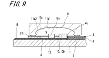
- FIG. 9 is an enlarged cross-sectional view showing a light emitting device according to another embodiment of the present disclosure.
- FIG. 9 shows an enlarged view of the element sealing region 9 and its vicinity.
- the same reference numerals are given to the parts corresponding to those of the above-described embodiment, and redundant explanations are omitted.
- the inner surface of the recess 11a is dome-shaped. With such a configuration, the amount of light received by the light receiving element 12 increases because the light is reflected by the light curved surface reaching the dome-shaped inner surface in the space of the element sealing region 9 .
- the curved surface may be shaped like a concave lens, for example, and the reflected light may be focused on the light receiving surface 12a to increase the amount of light received by the light receiving element 12.
- FIG. 9 has sides 11a2 sloping outwardly away from the cladding 3, but the sides 11a2 may be perpendicular to the cladding 3 in an upward direction or It may be inclined inwardly with respect to the clad 3 .
- the lid 11 shown in FIG. Although the lid 11 shown in FIG. Although the lid 11 shown in FIG.
- FIG. 10 is an enlarged cross-sectional view showing a light emitting device according to another embodiment of the present disclosure.
- FIG. 10 shows an enlarged view of the element sealing region 9 and its vicinity.
- the same reference numerals are given to the parts corresponding to those of the above-described embodiment, and redundant explanations are omitted.
- the inner surface of the recess 11a includes a roughened surface.
- the roughened surface may have a larger surface roughness than other surfaces other than the roughened surface, such as the outer surface. Since the light reaching the roughened surface is diffusely reflected, the amount of light received by the light receiving element 12 increases.
- the lid 11 shown in FIG. 10 does not include the reflective films 21 , 22 , 23 , but may include the reflective films 21 , 22 , 23 .
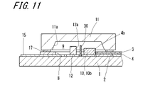
- FIG. 11 is an enlarged cross-sectional view showing a light emitting device according to another embodiment of the present disclosure.
- FIG. 11 shows an enlarged view of the element sealing region 9 and its vicinity.
- the same reference numerals are given to the parts corresponding to those of the above-described embodiment, and redundant explanations are omitted.
- the light receiving surface 12a of the light receiving element 12 faces the light emitting element 10, unlike the above embodiments.
- the light from the light emitting element 10 is directly received rather than the reflected light.
- a light diffusion member 30 is provided between the light receiving element 12 and the light emitting element 10 .
- the light from the light emitting element 10 is diffused by the light diffusing member 30, and the light receiving element 12 receives this diffused light.
- the arrangement position of the light diffusing member 30 may be adjusted so that the light receiving element 12 can receive the diffused light from the plurality of light emitting elements 10 .
- the light receiving element 12 receives the diffused light from the plurality of light emitting elements 10, the amount of received light can be suppressed. In addition, it becomes easy to adjust the arrangement of the light-emitting element 10 and the light-receiving element 12 .
- a diffraction grating or the like can be used as the light diffusion member 30 .
- FIG. 12 is an enlarged cross-sectional view showing a light emitting device according to still another embodiment of the present disclosure.
- FIG. 12 shows an enlarged view of the element sealing region 9 and its vicinity.
- the same reference numerals are given to the parts corresponding to those of the above-described embodiment, and redundant explanations are omitted.
- the lid 11 is not provided, but the sealing member 40 for sealing the light emitting element 10 and the light receiving element 12 is provided.
- the element sealing region 9 includes a sealing member 40 .
- the sealing member 40 is transparent to the light emitted from the light emitting element 10 , and the light receiving element 12 receives the light from the light emitting element 10 .
- the sealing member 40 may be transparent to the light emitted from the light emitting element 10, and may be, for example, a resin material or a glass material.
- a light receiving surface 12 a of the light receiving element 12 is the opposite surface of the surface facing the first surface 2 of the substrate 1 . This is the same as the configuration provided with the lid body 11 described above.
- the clad 3 does not have to have a portion (through hole 8) surrounding the light emitting element 10 and the light receiving element 12 as in the above-described embodiment.
- the light emitting element 10 and the light receiving element 12 may be mounted on the first surface 2 of the substrate 1 and sealed with the sealing member 40 while being connected to the external connection wiring 15 .
- the light-emitting device 100 can be miniaturized due to the configuration in which the light from the plurality of light-emitting elements 10 is received by the single light-receiving element 12 .
- the sealing member 40 has a fifth reflective film 51 on its outer surface.
- the fifth reflective film 51 can use, for example, a metal film such as aluminum, chromium, gold, or titanium, or a dielectric multilayer film.
- the fifth reflective film 51 By having the fifth reflective film 51 , the amount of reflected light increases in the sealing member 40 , so the amount of light received by the light receiving element 12 increases. Since the light-emitting element 10 can be highly adjusted by increasing the amount of light received by the light-receiving element 12, the light-emitting device 100 having this has excellent color tone adjustment capability.
- FIG. 13 is an enlarged cross-sectional view showing a light emitting device according to another embodiment of the present disclosure.
- FIG. 13 shows an enlarged view of the element sealing region 9 and its vicinity.
- the same reference numerals are given to the parts corresponding to those of the above-described embodiment, and redundant explanations are omitted.
- the clad 3 has the through hole 8
- the sealing member 40 is surrounded by the clad 3 in the direction along the first surface 2 of the substrate 1 .
- the sealing member 40 is formed by covering the light-emitting element 10 and the light-receiving element 12 in a softened or fluid state during sealing, and then curing the element.
- the sealing member 40 which is in a softened state or a fluid state during sealing, is placed in the clad 3. can be dammed up, and the sealing member 40 can be easily formed.
- FIG. 14 is an enlarged cross-sectional view showing a light emitting device according to another embodiment of the present disclosure.
- FIG. 14 shows an enlarged view of the element sealing region 9 and its vicinity.
- the same reference numerals are given to the parts corresponding to those of the above-described embodiment, and redundant explanations are omitted.
- the clad 3 has the through hole 8 and the sixth reflective film 52 is provided on the outer surface of the sealing member 40 .
- the sixth reflective film 52 for example, a metal film such as aluminum, chromium, gold, or titanium, or a dielectric multilayer film can be used.
- the sixth reflective film 52 extends from the outer surface of the outer surface of the sealing member 40 to above the clad 3 .
- the sealing member 40 is surrounded by the clad 3 and the sixth reflective film 52, so that leakage light is reduced and the amount of light received by the light receiving element 12 is increased.
- FIG. 15 is an enlarged cross-sectional view showing a light emitting device according to another embodiment of the present disclosure.
- FIG. 15 shows an enlarged view of the element sealing region 9 and its vicinity.
- the same reference numerals are given to the parts corresponding to those of the above-described embodiment, and redundant explanations are omitted.
- the outer surface of the sealing member 40 includes a roughened surface. It is sufficient that the roughened surface has a larger surface roughness than the surfaces other than the roughened surface. Since the light reaching the roughened surface is diffusely reflected, the amount of light received by the light receiving element 12 increases.
- the sealing member 40 shown in FIG. 15 does not include the sixth reflective film 52, but may include the sixth reflective film 52.
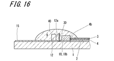
- FIG. 16 is an enlarged cross-sectional view showing a light emitting device according to another embodiment of the present disclosure.
- FIG. 16 shows an enlarged view of the element sealing region 9 and its vicinity.
- the same reference numerals are given to the parts corresponding to those of the above-described embodiment, and redundant explanations are omitted.
- the light receiving surface 12a of the light receiving element 12 faces the light emitting element 10, and the light diffusion member 30 is provided between the light receiving element 12 and the light emitting element 10.
- the sealing member 40 the light from the light emitting element 10 is diffused by the light diffusing member 30, and the light receiving element 12 receives this diffused light.
- the arrangement position of the light diffusing member 30 may be adjusted so that the light receiving element 12 can receive the diffused light from the plurality of light emitting elements 10 . Since the light receiving element 12 receives the diffused light from the plurality of light emitting elements 10, the amount of received light can be suppressed. In addition, it becomes easy to adjust the arrangement of the light-emitting element 10 and the light-receiving element 12 .
- a diffraction grating or the like can be used as the light diffusion member 30 .
- the light receiving surface 12a of the light receiving element 12 faces the light emitting element 10, and a reflector such as a mirror may be arranged between the light receiving element 12 and the light emitting element 10. .
- a reflector is arranged for each light emitting element 10 and the angle of reflection is adjusted. Light from the first light emitting element 10 a is reflected by the first reflector and received by the light receiving element 12 . Light from the second light emitting element 10 b is reflected by the second reflector and received by the light receiving element 12 . Light from the third light emitting element 10 c is reflected by the third reflector and received by the light receiving element 12 .
Landscapes
- Physics & Mathematics (AREA)
- General Physics & Mathematics (AREA)
- Optics & Photonics (AREA)
- Condensed Matter Physics & Semiconductors (AREA)
- Electromagnetism (AREA)
- Led Device Packages (AREA)
Priority Applications (4)
| Application Number | Priority Date | Filing Date | Title |
|---|---|---|---|
| CN202280014695.1A CN116829999A (zh) | 2021-02-19 | 2022-02-18 | 发光装置 |
| EP22756304.6A EP4297205A1 (en) | 2021-02-19 | 2022-02-18 | Light emitting device |
| US18/277,245 US20240094486A1 (en) | 2021-02-19 | 2022-02-18 | Light emitter |
| JP2023500947A JP7642782B2 (ja) | 2021-02-19 | 2022-02-18 | 発光装置 |
Applications Claiming Priority (2)
| Application Number | Priority Date | Filing Date | Title |
|---|---|---|---|
| JP2021025665 | 2021-02-19 | ||
| JP2021-025665 | 2021-02-19 |
Publications (1)
| Publication Number | Publication Date |
|---|---|
| WO2022176987A1 true WO2022176987A1 (ja) | 2022-08-25 |
Family
ID=82930642
Family Applications (1)
| Application Number | Title | Priority Date | Filing Date |
|---|---|---|---|
| PCT/JP2022/006736 Ceased WO2022176987A1 (ja) | 2021-02-19 | 2022-02-18 | 発光装置 |
Country Status (5)
| Country | Link |
|---|---|
| US (1) | US20240094486A1 (https=) |
| EP (1) | EP4297205A1 (https=) |
| JP (1) | JP7642782B2 (https=) |
| CN (1) | CN116829999A (https=) |
| WO (1) | WO2022176987A1 (https=) |
Citations (8)
| Publication number | Priority date | Publication date | Assignee | Title |
|---|---|---|---|---|
| JPH05175614A (ja) * | 1991-12-26 | 1993-07-13 | Canon Inc | 光半導体装置 |
| JPH10300990A (ja) * | 1997-04-22 | 1998-11-13 | Sharp Corp | 光結合半導体装置 |
| US20030002826A1 (en) * | 2001-06-27 | 2003-01-02 | International Business Machines Corporation | Light emitter control system |
| JP2004207911A (ja) | 2002-12-24 | 2004-07-22 | Seiko Epson Corp | 光学ユニット、光源制御装置、光強度制御装置、光通信装置 |
| JP2009186578A (ja) * | 2008-02-04 | 2009-08-20 | Fuji Xerox Co Ltd | 光導波部材、光モジュール、及び光伝送装置 |
| JP2010237483A (ja) * | 2009-03-31 | 2010-10-21 | Anritsu Corp | 光変調器モジュール |
| WO2014091551A1 (ja) * | 2012-12-11 | 2014-06-19 | パイオニア株式会社 | 光源ユニット、光源ユニットの制御方法、プログラム及び記録媒体 |
| US20190296522A1 (en) * | 2018-03-20 | 2019-09-26 | Vixar, Inc. | Eye safe optical modules |
Family Cites Families (4)
| Publication number | Priority date | Publication date | Assignee | Title |
|---|---|---|---|---|
| JP4445270B2 (ja) * | 2002-03-28 | 2010-04-07 | 富士通株式会社 | レーザアレー装置及びレーザアレー制御方法 |
| JP2004064013A (ja) * | 2002-07-31 | 2004-02-26 | Kinseki Ltd | 電子部品用パッケ−ジのキャップ封止方法 |
| JP6205001B2 (ja) * | 2016-01-14 | 2017-09-27 | 株式会社フジクラ | 光電変換モジュール、及び、アクティブ光ケーブル |
| DE102020110658A1 (de) * | 2020-04-20 | 2021-10-21 | Schott Ag | Multilaser-Anordnung, insbesondere RGB-Lasermodul sowie diese umfassende Vorrichtungen |
-
2022
- 2022-02-18 EP EP22756304.6A patent/EP4297205A1/en not_active Withdrawn
- 2022-02-18 WO PCT/JP2022/006736 patent/WO2022176987A1/ja not_active Ceased
- 2022-02-18 JP JP2023500947A patent/JP7642782B2/ja active Active
- 2022-02-18 US US18/277,245 patent/US20240094486A1/en active Pending
- 2022-02-18 CN CN202280014695.1A patent/CN116829999A/zh active Pending
Patent Citations (8)
| Publication number | Priority date | Publication date | Assignee | Title |
|---|---|---|---|---|
| JPH05175614A (ja) * | 1991-12-26 | 1993-07-13 | Canon Inc | 光半導体装置 |
| JPH10300990A (ja) * | 1997-04-22 | 1998-11-13 | Sharp Corp | 光結合半導体装置 |
| US20030002826A1 (en) * | 2001-06-27 | 2003-01-02 | International Business Machines Corporation | Light emitter control system |
| JP2004207911A (ja) | 2002-12-24 | 2004-07-22 | Seiko Epson Corp | 光学ユニット、光源制御装置、光強度制御装置、光通信装置 |
| JP2009186578A (ja) * | 2008-02-04 | 2009-08-20 | Fuji Xerox Co Ltd | 光導波部材、光モジュール、及び光伝送装置 |
| JP2010237483A (ja) * | 2009-03-31 | 2010-10-21 | Anritsu Corp | 光変調器モジュール |
| WO2014091551A1 (ja) * | 2012-12-11 | 2014-06-19 | パイオニア株式会社 | 光源ユニット、光源ユニットの制御方法、プログラム及び記録媒体 |
| US20190296522A1 (en) * | 2018-03-20 | 2019-09-26 | Vixar, Inc. | Eye safe optical modules |
Also Published As
| Publication number | Publication date |
|---|---|
| EP4297205A1 (en) | 2023-12-27 |
| JPWO2022176987A1 (https=) | 2022-08-25 |
| CN116829999A (zh) | 2023-09-29 |
| JP7642782B2 (ja) | 2025-03-10 |
| US20240094486A1 (en) | 2024-03-21 |
Similar Documents
| Publication | Publication Date | Title |
|---|---|---|
| JP7339591B2 (ja) | 発光モジュールの製造方法、発光モジュール及びプロジェクタ | |
| CN115867841A (zh) | 光波导封装件、发光装置及投影系统 | |
| JP7157346B2 (ja) | 発光装置 | |
| JP2019207976A (ja) | 光源装置 | |
| US11811190B2 (en) | Light-emitting device | |
| US20090121248A1 (en) | Semiconductor light emitting device and planar light source | |
| JP2023127591A (ja) | 光導波路パッケージおよび発光装置 | |
| CN101828136B (zh) | 用于背光应用的侧面发光led光源 | |
| WO2022176992A1 (ja) | 発光装置 | |
| US12124079B2 (en) | Optical waveguide package and light-emitting device | |
| JP7642782B2 (ja) | 発光装置 | |
| JP2013197450A (ja) | 発光装置およびその製造方法 | |
| US12222540B2 (en) | Optical waveguide package and light-emitting device | |
| WO2023153419A1 (ja) | 光導波路基板、光導波路パッケージおよび光源モジュール | |
| JP2025165179A (ja) | 発光装置 | |
| TW202346930A (zh) | 光波導基板、光波導封裝及光源模組 | |
| WO2024204657A1 (ja) | 光導波路パッケージ及び光源モジュール | |
| US10082271B2 (en) | Laser light optical module utilizing reflective films for improved efficiency | |
| JP2026004719A (ja) | 光導波路、電子素子収納用パッケージ、電子モジュール及び電子デバイス | |
| JP2023123752A (ja) | 光導波路モジュール | |
| WO2024128324A1 (ja) | 発光装置 | |
| CN119768718A (zh) | 光波导封装件 | |
| CN121241285A (zh) | 具有集成微型led的光子集成电路 | |
| JPWO2022176987A5 (https=) |
Legal Events
| Date | Code | Title | Description |
|---|---|---|---|
| 121 | Ep: the epo has been informed by wipo that ep was designated in this application |
Ref document number: 22756304 Country of ref document: EP Kind code of ref document: A1 |
|
| WWE | Wipo information: entry into national phase |
Ref document number: 202280014695.1 Country of ref document: CN |
|
| WWE | Wipo information: entry into national phase |
Ref document number: 18277245 Country of ref document: US |
|
| WWE | Wipo information: entry into national phase |
Ref document number: 2023500947 Country of ref document: JP |
|
| WWE | Wipo information: entry into national phase |
Ref document number: 2022756304 Country of ref document: EP |
|
| NENP | Non-entry into the national phase |
Ref country code: DE |
|
| ENP | Entry into the national phase |
Ref document number: 2022756304 Country of ref document: EP Effective date: 20230919 |