WO2022176434A1 - レーザ素子、レーザ素子アレイ及びレーザ素子の製造方法 - Google Patents
レーザ素子、レーザ素子アレイ及びレーザ素子の製造方法 Download PDFInfo
- Publication number
- WO2022176434A1 WO2022176434A1 PCT/JP2022/000513 JP2022000513W WO2022176434A1 WO 2022176434 A1 WO2022176434 A1 WO 2022176434A1 JP 2022000513 W JP2022000513 W JP 2022000513W WO 2022176434 A1 WO2022176434 A1 WO 2022176434A1
- Authority
- WO
- WIPO (PCT)
- Prior art keywords
- lens
- layer
- laser device
- light reflecting
- light
- Prior art date
Links
- 238000004519 manufacturing process Methods 0.000 title claims abstract description 40
- 230000003287 optical effect Effects 0.000 claims abstract description 44
- 239000004065 semiconductor Substances 0.000 claims description 179
- 239000000463 material Substances 0.000 claims description 95
- 238000002347 injection Methods 0.000 claims description 67
- 239000007924 injection Substances 0.000 claims description 67
- 238000006243 chemical reaction Methods 0.000 claims description 53
- 238000000034 method Methods 0.000 claims description 35
- 238000005530 etching Methods 0.000 claims description 21
- 239000012530 fluid Substances 0.000 claims description 19
- 238000005215 recombination Methods 0.000 claims description 15
- 230000006798 recombination Effects 0.000 claims description 15
- 238000010030 laminating Methods 0.000 claims description 9
- 229910001218 Gallium arsenide Inorganic materials 0.000 claims description 8
- 239000012141 concentrate Substances 0.000 claims description 5
- 238000001312 dry etching Methods 0.000 claims description 5
- 238000001039 wet etching Methods 0.000 claims description 5
- 238000005516 engineering process Methods 0.000 abstract description 16
- 239000010410 layer Substances 0.000 description 424
- 239000000758 substrate Substances 0.000 description 37
- 238000010586 diagram Methods 0.000 description 31
- 239000010408 film Substances 0.000 description 23
- 150000002500 ions Chemical class 0.000 description 18
- 239000002245 particle Substances 0.000 description 15
- OAICVXFJPJFONN-UHFFFAOYSA-N Phosphorus Chemical compound [P] OAICVXFJPJFONN-UHFFFAOYSA-N 0.000 description 13
- 229910004298 SiO 2 Inorganic materials 0.000 description 12
- 229910052751 metal Inorganic materials 0.000 description 11
- 239000002184 metal Substances 0.000 description 11
- 239000002096 quantum dot Substances 0.000 description 11
- 230000000694 effects Effects 0.000 description 10
- 229910052737 gold Inorganic materials 0.000 description 10
- 229910052759 nickel Inorganic materials 0.000 description 10
- 238000010438 heat treatment Methods 0.000 description 9
- 230000002093 peripheral effect Effects 0.000 description 9
- 229910052771 Terbium Inorganic materials 0.000 description 8
- 239000000969 carrier Substances 0.000 description 7
- 230000007423 decrease Effects 0.000 description 7
- 230000010355 oscillation Effects 0.000 description 7
- 230000002269 spontaneous effect Effects 0.000 description 7
- VYPSYNLAJGMNEJ-UHFFFAOYSA-N Silicium dioxide Chemical compound O=[Si]=O VYPSYNLAJGMNEJ-UHFFFAOYSA-N 0.000 description 6
- 230000004888 barrier function Effects 0.000 description 6
- 239000012535 impurity Substances 0.000 description 6
- 239000000203 mixture Substances 0.000 description 6
- 229910052782 aluminium Inorganic materials 0.000 description 5
- 229910052763 palladium Inorganic materials 0.000 description 5
- 238000000206 photolithography Methods 0.000 description 5
- 230000005855 radiation Effects 0.000 description 5
- 229910052709 silver Inorganic materials 0.000 description 5
- 239000002356 single layer Substances 0.000 description 5
- 229910052684 Cerium Inorganic materials 0.000 description 4
- XLOMVQKBTHCTTD-UHFFFAOYSA-N Zinc monoxide Chemical compound [Zn]=O XLOMVQKBTHCTTD-UHFFFAOYSA-N 0.000 description 4
- 230000009969 flowable effect Effects 0.000 description 4
- 238000005468 ion implantation Methods 0.000 description 4
- 229910052749 magnesium Inorganic materials 0.000 description 4
- 229910052757 nitrogen Inorganic materials 0.000 description 4
- 238000001020 plasma etching Methods 0.000 description 4
- 229910052712 strontium Inorganic materials 0.000 description 4
- 229910020068 MgAl Inorganic materials 0.000 description 3
- JNDMLEXHDPKVFC-UHFFFAOYSA-N aluminum;oxygen(2-);yttrium(3+) Chemical compound [O-2].[O-2].[O-2].[Al+3].[Y+3] JNDMLEXHDPKVFC-UHFFFAOYSA-N 0.000 description 3
- 229910052788 barium Inorganic materials 0.000 description 3
- 229910052791 calcium Inorganic materials 0.000 description 3
- 238000005229 chemical vapour deposition Methods 0.000 description 3
- 229910052681 coesite Inorganic materials 0.000 description 3
- 229910052906 cristobalite Inorganic materials 0.000 description 3
- 230000005484 gravity Effects 0.000 description 3
- 229910052748 manganese Inorganic materials 0.000 description 3
- 239000012788 optical film Substances 0.000 description 3
- 229910052760 oxygen Inorganic materials 0.000 description 3
- 230000008569 process Effects 0.000 description 3
- 229910052710 silicon Inorganic materials 0.000 description 3
- 239000000377 silicon dioxide Substances 0.000 description 3
- 235000012239 silicon dioxide Nutrition 0.000 description 3
- 229910052682 stishovite Inorganic materials 0.000 description 3
- 230000032258 transport Effects 0.000 description 3
- 229910052905 tridymite Inorganic materials 0.000 description 3
- 229910019901 yttrium aluminum garnet Inorganic materials 0.000 description 3
- 229910000980 Aluminium gallium arsenide Inorganic materials 0.000 description 2
- ZOXJGFHDIHLPTG-UHFFFAOYSA-N Boron Chemical compound [B] ZOXJGFHDIHLPTG-UHFFFAOYSA-N 0.000 description 2
- 229910004829 CaWO4 Inorganic materials 0.000 description 2
- UFHFLCQGNIYNRP-UHFFFAOYSA-N Hydrogen Chemical compound [H][H] UFHFLCQGNIYNRP-UHFFFAOYSA-N 0.000 description 2
- 229910010413 TiO 2 Inorganic materials 0.000 description 2
- QVGXLLKOCUKJST-UHFFFAOYSA-N atomic oxygen Chemical compound [O] QVGXLLKOCUKJST-UHFFFAOYSA-N 0.000 description 2
- 229910052796 boron Inorganic materials 0.000 description 2
- 229910052739 hydrogen Inorganic materials 0.000 description 2
- 239000001257 hydrogen Substances 0.000 description 2
- 239000011810 insulating material Substances 0.000 description 2
- ZKATWMILCYLAPD-UHFFFAOYSA-N niobium pentoxide Chemical compound O=[Nb](=O)O[Nb](=O)=O ZKATWMILCYLAPD-UHFFFAOYSA-N 0.000 description 2
- 230000003647 oxidation Effects 0.000 description 2
- 238000007254 oxidation reaction Methods 0.000 description 2
- 239000001301 oxygen Substances 0.000 description 2
- 238000000059 patterning Methods 0.000 description 2
- 238000004528 spin coating Methods 0.000 description 2
- 229910052719 titanium Inorganic materials 0.000 description 2
- 239000011787 zinc oxide Substances 0.000 description 2
- YBNMDCCMCLUHBL-UHFFFAOYSA-N (2,5-dioxopyrrolidin-1-yl) 4-pyren-1-ylbutanoate Chemical compound C=1C=C(C2=C34)C=CC3=CC=CC4=CC=C2C=1CCCC(=O)ON1C(=O)CCC1=O YBNMDCCMCLUHBL-UHFFFAOYSA-N 0.000 description 1
- 102100032047 Alsin Human genes 0.000 description 1
- 101710187109 Alsin Proteins 0.000 description 1
- OKTJSMMVPCPJKN-UHFFFAOYSA-N Carbon Chemical compound [C] OKTJSMMVPCPJKN-UHFFFAOYSA-N 0.000 description 1
- 229910004613 CdTe Inorganic materials 0.000 description 1
- 229910052693 Europium Inorganic materials 0.000 description 1
- 229910000530 Gallium indium arsenide Inorganic materials 0.000 description 1
- 229910004262 HgTe Inorganic materials 0.000 description 1
- 229910000673 Indium arsenide Inorganic materials 0.000 description 1
- 229910001477 LaPO4 Inorganic materials 0.000 description 1
- 229910006404 SnO 2 Inorganic materials 0.000 description 1
- GWEVSGVZZGPLCZ-UHFFFAOYSA-N Titan oxide Chemical compound O=[Ti]=O GWEVSGVZZGPLCZ-UHFFFAOYSA-N 0.000 description 1
- 229910009372 YVO4 Inorganic materials 0.000 description 1
- 229910052769 Ytterbium Inorganic materials 0.000 description 1
- 229910007709 ZnTe Inorganic materials 0.000 description 1
- 230000009471 action Effects 0.000 description 1
- XAGFODPZIPBFFR-UHFFFAOYSA-N aluminium Chemical compound [Al] XAGFODPZIPBFFR-UHFFFAOYSA-N 0.000 description 1
- UHYPYGJEEGLRJD-UHFFFAOYSA-N cadmium(2+);selenium(2-) Chemical compound [Se-2].[Cd+2] UHYPYGJEEGLRJD-UHFFFAOYSA-N 0.000 description 1
- 229910052956 cinnabar Inorganic materials 0.000 description 1
- 230000001427 coherent effect Effects 0.000 description 1
- 150000001875 compounds Chemical class 0.000 description 1
- 239000004020 conductor Substances 0.000 description 1
- 239000000470 constituent Substances 0.000 description 1
- 239000011258 core-shell material Substances 0.000 description 1
- 230000000994 depressogenic effect Effects 0.000 description 1
- 238000009826 distribution Methods 0.000 description 1
- 238000010894 electron beam technology Methods 0.000 description 1
- 239000011521 glass Substances 0.000 description 1
- 229910021389 graphene Inorganic materials 0.000 description 1
- 229910052738 indium Inorganic materials 0.000 description 1
- RPQDHPTXJYYUPQ-UHFFFAOYSA-N indium arsenide Chemical compound [In]#[As] RPQDHPTXJYYUPQ-UHFFFAOYSA-N 0.000 description 1
- APFVFJFRJDLVQX-UHFFFAOYSA-N indium atom Chemical compound [In] APFVFJFRJDLVQX-UHFFFAOYSA-N 0.000 description 1
- AMGQUBHHOARCQH-UHFFFAOYSA-N indium;oxotin Chemical compound [In].[Sn]=O AMGQUBHHOARCQH-UHFFFAOYSA-N 0.000 description 1
- 238000009413 insulation Methods 0.000 description 1
- 229910052745 lead Inorganic materials 0.000 description 1
- 230000000670 limiting effect Effects 0.000 description 1
- 229910052744 lithium Inorganic materials 0.000 description 1
- 230000008018 melting Effects 0.000 description 1
- 238000002844 melting Methods 0.000 description 1
- 239000011368 organic material Substances 0.000 description 1
- 230000001151 other effect Effects 0.000 description 1
- 230000001590 oxidative effect Effects 0.000 description 1
- 229910052698 phosphorus Inorganic materials 0.000 description 1
- 229920002120 photoresistant polymer Polymers 0.000 description 1
- 150000002910 rare earth metals Chemical group 0.000 description 1
- SBIBMFFZSBJNJF-UHFFFAOYSA-N selenium;zinc Chemical compound [Se]=[Zn] SBIBMFFZSBJNJF-UHFFFAOYSA-N 0.000 description 1
- 239000010703 silicon Substances 0.000 description 1
- 229910052950 sphalerite Inorganic materials 0.000 description 1
- 238000004544 sputter deposition Methods 0.000 description 1
- PBCFLUZVCVVTBY-UHFFFAOYSA-N tantalum pentoxide Inorganic materials O=[Ta](=O)O[Ta](=O)=O PBCFLUZVCVVTBY-UHFFFAOYSA-N 0.000 description 1
- OGIDPMRJRNCKJF-UHFFFAOYSA-N titanium oxide Inorganic materials [Ti]=O OGIDPMRJRNCKJF-UHFFFAOYSA-N 0.000 description 1
- 230000007704 transition Effects 0.000 description 1
- 238000001771 vacuum deposition Methods 0.000 description 1
- XLYOFNOQVPJJNP-UHFFFAOYSA-N water Chemical compound O XLYOFNOQVPJJNP-UHFFFAOYSA-N 0.000 description 1
- 230000005428 wave function Effects 0.000 description 1
- 229910052844 willemite Inorganic materials 0.000 description 1
- 229910052882 wollastonite Inorganic materials 0.000 description 1
- 229910052727 yttrium Inorganic materials 0.000 description 1
- 229910052984 zinc sulfide Inorganic materials 0.000 description 1
Images


Classifications
-
- H—ELECTRICITY
- H01—ELECTRIC ELEMENTS
- H01S—DEVICES USING THE PROCESS OF LIGHT AMPLIFICATION BY STIMULATED EMISSION OF RADIATION [LASER] TO AMPLIFY OR GENERATE LIGHT; DEVICES USING STIMULATED EMISSION OF ELECTROMAGNETIC RADIATION IN WAVE RANGES OTHER THAN OPTICAL
- H01S5/00—Semiconductor lasers
- H01S5/02—Structural details or components not essential to laser action
- H01S5/0206—Substrates, e.g. growth, shape, material, removal or bonding
- H01S5/0207—Substrates having a special shape
-
- H—ELECTRICITY
- H01—ELECTRIC ELEMENTS
- H01S—DEVICES USING THE PROCESS OF LIGHT AMPLIFICATION BY STIMULATED EMISSION OF RADIATION [LASER] TO AMPLIFY OR GENERATE LIGHT; DEVICES USING STIMULATED EMISSION OF ELECTROMAGNETIC RADIATION IN WAVE RANGES OTHER THAN OPTICAL
- H01S5/00—Semiconductor lasers
- H01S5/10—Construction or shape of the optical resonator, e.g. extended or external cavity, coupled cavities, bent-guide, varying width, thickness or composition of the active region
- H01S5/18—Surface-emitting [SE] lasers, e.g. having both horizontal and vertical cavities
-
- H—ELECTRICITY
- H01—ELECTRIC ELEMENTS
- H01S—DEVICES USING THE PROCESS OF LIGHT AMPLIFICATION BY STIMULATED EMISSION OF RADIATION [LASER] TO AMPLIFY OR GENERATE LIGHT; DEVICES USING STIMULATED EMISSION OF ELECTROMAGNETIC RADIATION IN WAVE RANGES OTHER THAN OPTICAL
- H01S5/00—Semiconductor lasers
- H01S5/02—Structural details or components not essential to laser action
- H01S5/026—Monolithically integrated components, e.g. waveguides, monitoring photo-detectors, drivers
-
- H—ELECTRICITY
- H01—ELECTRIC ELEMENTS
- H01S—DEVICES USING THE PROCESS OF LIGHT AMPLIFICATION BY STIMULATED EMISSION OF RADIATION [LASER] TO AMPLIFY OR GENERATE LIGHT; DEVICES USING STIMULATED EMISSION OF ELECTROMAGNETIC RADIATION IN WAVE RANGES OTHER THAN OPTICAL
- H01S5/00—Semiconductor lasers
- H01S5/10—Construction or shape of the optical resonator, e.g. extended or external cavity, coupled cavities, bent-guide, varying width, thickness or composition of the active region
- H01S5/18—Surface-emitting [SE] lasers, e.g. having both horizontal and vertical cavities
- H01S5/183—Surface-emitting [SE] lasers, e.g. having both horizontal and vertical cavities having only vertical cavities, e.g. vertical cavity surface-emitting lasers [VCSEL]
- H01S5/18308—Surface-emitting [SE] lasers, e.g. having both horizontal and vertical cavities having only vertical cavities, e.g. vertical cavity surface-emitting lasers [VCSEL] having a special structure for lateral current or light confinement
- H01S5/18338—Non-circular shape of the structure
-
- H—ELECTRICITY
- H01—ELECTRIC ELEMENTS
- H01S—DEVICES USING THE PROCESS OF LIGHT AMPLIFICATION BY STIMULATED EMISSION OF RADIATION [LASER] TO AMPLIFY OR GENERATE LIGHT; DEVICES USING STIMULATED EMISSION OF ELECTROMAGNETIC RADIATION IN WAVE RANGES OTHER THAN OPTICAL
- H01S5/00—Semiconductor lasers
- H01S5/10—Construction or shape of the optical resonator, e.g. extended or external cavity, coupled cavities, bent-guide, varying width, thickness or composition of the active region
- H01S5/18—Surface-emitting [SE] lasers, e.g. having both horizontal and vertical cavities
- H01S5/183—Surface-emitting [SE] lasers, e.g. having both horizontal and vertical cavities having only vertical cavities, e.g. vertical cavity surface-emitting lasers [VCSEL]
- H01S5/18361—Structure of the reflectors, e.g. hybrid mirrors
-
- H—ELECTRICITY
- H01—ELECTRIC ELEMENTS
- H01S—DEVICES USING THE PROCESS OF LIGHT AMPLIFICATION BY STIMULATED EMISSION OF RADIATION [LASER] TO AMPLIFY OR GENERATE LIGHT; DEVICES USING STIMULATED EMISSION OF ELECTROMAGNETIC RADIATION IN WAVE RANGES OTHER THAN OPTICAL
- H01S5/00—Semiconductor lasers
- H01S5/30—Structure or shape of the active region; Materials used for the active region
- H01S5/34—Structure or shape of the active region; Materials used for the active region comprising quantum well or superlattice structures, e.g. single quantum well [SQW] lasers, multiple quantum well [MQW] lasers or graded index separate confinement heterostructure [GRINSCH] lasers
- H01S5/343—Structure or shape of the active region; Materials used for the active region comprising quantum well or superlattice structures, e.g. single quantum well [SQW] lasers, multiple quantum well [MQW] lasers or graded index separate confinement heterostructure [GRINSCH] lasers in AIIIBV compounds, e.g. AlGaAs-laser, InP-based laser
- H01S5/34313—Structure or shape of the active region; Materials used for the active region comprising quantum well or superlattice structures, e.g. single quantum well [SQW] lasers, multiple quantum well [MQW] lasers or graded index separate confinement heterostructure [GRINSCH] lasers in AIIIBV compounds, e.g. AlGaAs-laser, InP-based laser with a well layer having only As as V-compound, e.g. AlGaAs, InGaAs
- H01S5/3432—Structure or shape of the active region; Materials used for the active region comprising quantum well or superlattice structures, e.g. single quantum well [SQW] lasers, multiple quantum well [MQW] lasers or graded index separate confinement heterostructure [GRINSCH] lasers in AIIIBV compounds, e.g. AlGaAs-laser, InP-based laser with a well layer having only As as V-compound, e.g. AlGaAs, InGaAs the whole junction comprising only (AI)GaAs
-
- H—ELECTRICITY
- H01—ELECTRIC ELEMENTS
- H01S—DEVICES USING THE PROCESS OF LIGHT AMPLIFICATION BY STIMULATED EMISSION OF RADIATION [LASER] TO AMPLIFY OR GENERATE LIGHT; DEVICES USING STIMULATED EMISSION OF ELECTROMAGNETIC RADIATION IN WAVE RANGES OTHER THAN OPTICAL
- H01S5/00—Semiconductor lasers
- H01S5/30—Structure or shape of the active region; Materials used for the active region
- H01S5/34—Structure or shape of the active region; Materials used for the active region comprising quantum well or superlattice structures, e.g. single quantum well [SQW] lasers, multiple quantum well [MQW] lasers or graded index separate confinement heterostructure [GRINSCH] lasers
- H01S5/343—Structure or shape of the active region; Materials used for the active region comprising quantum well or superlattice structures, e.g. single quantum well [SQW] lasers, multiple quantum well [MQW] lasers or graded index separate confinement heterostructure [GRINSCH] lasers in AIIIBV compounds, e.g. AlGaAs-laser, InP-based laser
- H01S5/3434—Structure or shape of the active region; Materials used for the active region comprising quantum well or superlattice structures, e.g. single quantum well [SQW] lasers, multiple quantum well [MQW] lasers or graded index separate confinement heterostructure [GRINSCH] lasers in AIIIBV compounds, e.g. AlGaAs-laser, InP-based laser with a well layer comprising at least both As and P as V-compounds
-
- H—ELECTRICITY
- H01—ELECTRIC ELEMENTS
- H01S—DEVICES USING THE PROCESS OF LIGHT AMPLIFICATION BY STIMULATED EMISSION OF RADIATION [LASER] TO AMPLIFY OR GENERATE LIGHT; DEVICES USING STIMULATED EMISSION OF ELECTROMAGNETIC RADIATION IN WAVE RANGES OTHER THAN OPTICAL
- H01S5/00—Semiconductor lasers
- H01S5/30—Structure or shape of the active region; Materials used for the active region
- H01S5/34—Structure or shape of the active region; Materials used for the active region comprising quantum well or superlattice structures, e.g. single quantum well [SQW] lasers, multiple quantum well [MQW] lasers or graded index separate confinement heterostructure [GRINSCH] lasers
- H01S5/343—Structure or shape of the active region; Materials used for the active region comprising quantum well or superlattice structures, e.g. single quantum well [SQW] lasers, multiple quantum well [MQW] lasers or graded index separate confinement heterostructure [GRINSCH] lasers in AIIIBV compounds, e.g. AlGaAs-laser, InP-based laser
- H01S5/34346—Structure or shape of the active region; Materials used for the active region comprising quantum well or superlattice structures, e.g. single quantum well [SQW] lasers, multiple quantum well [MQW] lasers or graded index separate confinement heterostructure [GRINSCH] lasers in AIIIBV compounds, e.g. AlGaAs-laser, InP-based laser characterised by the materials of the barrier layers
- H01S5/34353—Structure or shape of the active region; Materials used for the active region comprising quantum well or superlattice structures, e.g. single quantum well [SQW] lasers, multiple quantum well [MQW] lasers or graded index separate confinement heterostructure [GRINSCH] lasers in AIIIBV compounds, e.g. AlGaAs-laser, InP-based laser characterised by the materials of the barrier layers based on (AI)GaAs
-
- H—ELECTRICITY
- H01—ELECTRIC ELEMENTS
- H01S—DEVICES USING THE PROCESS OF LIGHT AMPLIFICATION BY STIMULATED EMISSION OF RADIATION [LASER] TO AMPLIFY OR GENERATE LIGHT; DEVICES USING STIMULATED EMISSION OF ELECTROMAGNETIC RADIATION IN WAVE RANGES OTHER THAN OPTICAL
- H01S5/00—Semiconductor lasers
- H01S5/30—Structure or shape of the active region; Materials used for the active region
- H01S5/34—Structure or shape of the active region; Materials used for the active region comprising quantum well or superlattice structures, e.g. single quantum well [SQW] lasers, multiple quantum well [MQW] lasers or graded index separate confinement heterostructure [GRINSCH] lasers
- H01S5/343—Structure or shape of the active region; Materials used for the active region comprising quantum well or superlattice structures, e.g. single quantum well [SQW] lasers, multiple quantum well [MQW] lasers or graded index separate confinement heterostructure [GRINSCH] lasers in AIIIBV compounds, e.g. AlGaAs-laser, InP-based laser
- H01S5/34346—Structure or shape of the active region; Materials used for the active region comprising quantum well or superlattice structures, e.g. single quantum well [SQW] lasers, multiple quantum well [MQW] lasers or graded index separate confinement heterostructure [GRINSCH] lasers in AIIIBV compounds, e.g. AlGaAs-laser, InP-based laser characterised by the materials of the barrier layers
- H01S5/34373—Structure or shape of the active region; Materials used for the active region comprising quantum well or superlattice structures, e.g. single quantum well [SQW] lasers, multiple quantum well [MQW] lasers or graded index separate confinement heterostructure [GRINSCH] lasers in AIIIBV compounds, e.g. AlGaAs-laser, InP-based laser characterised by the materials of the barrier layers based on InGa(Al)AsP
-
- H—ELECTRICITY
- H01—ELECTRIC ELEMENTS
- H01S—DEVICES USING THE PROCESS OF LIGHT AMPLIFICATION BY STIMULATED EMISSION OF RADIATION [LASER] TO AMPLIFY OR GENERATE LIGHT; DEVICES USING STIMULATED EMISSION OF ELECTROMAGNETIC RADIATION IN WAVE RANGES OTHER THAN OPTICAL
- H01S5/00—Semiconductor lasers
- H01S5/40—Arrangement of two or more semiconductor lasers, not provided for in groups H01S5/02 - H01S5/30
- H01S5/42—Arrays of surface emitting lasers
-
- H—ELECTRICITY
- H01—ELECTRIC ELEMENTS
- H01S—DEVICES USING THE PROCESS OF LIGHT AMPLIFICATION BY STIMULATED EMISSION OF RADIATION [LASER] TO AMPLIFY OR GENERATE LIGHT; DEVICES USING STIMULATED EMISSION OF ELECTROMAGNETIC RADIATION IN WAVE RANGES OTHER THAN OPTICAL
- H01S5/00—Semiconductor lasers
- H01S5/04—Processes or apparatus for excitation, e.g. pumping, e.g. by electron beams
- H01S5/042—Electrical excitation ; Circuits therefor
- H01S5/0425—Electrodes, e.g. characterised by the structure
- H01S5/04252—Electrodes, e.g. characterised by the structure characterised by the material
- H01S5/04253—Electrodes, e.g. characterised by the structure characterised by the material having specific optical properties, e.g. transparent electrodes
-
- H—ELECTRICITY
- H01—ELECTRIC ELEMENTS
- H01S—DEVICES USING THE PROCESS OF LIGHT AMPLIFICATION BY STIMULATED EMISSION OF RADIATION [LASER] TO AMPLIFY OR GENERATE LIGHT; DEVICES USING STIMULATED EMISSION OF ELECTROMAGNETIC RADIATION IN WAVE RANGES OTHER THAN OPTICAL
- H01S5/00—Semiconductor lasers
- H01S5/04—Processes or apparatus for excitation, e.g. pumping, e.g. by electron beams
- H01S5/042—Electrical excitation ; Circuits therefor
- H01S5/0425—Electrodes, e.g. characterised by the structure
- H01S5/04256—Electrodes, e.g. characterised by the structure characterised by the configuration
-
- H—ELECTRICITY
- H01—ELECTRIC ELEMENTS
- H01S—DEVICES USING THE PROCESS OF LIGHT AMPLIFICATION BY STIMULATED EMISSION OF RADIATION [LASER] TO AMPLIFY OR GENERATE LIGHT; DEVICES USING STIMULATED EMISSION OF ELECTROMAGNETIC RADIATION IN WAVE RANGES OTHER THAN OPTICAL
- H01S5/00—Semiconductor lasers
- H01S5/10—Construction or shape of the optical resonator, e.g. extended or external cavity, coupled cavities, bent-guide, varying width, thickness or composition of the active region
- H01S5/18—Surface-emitting [SE] lasers, e.g. having both horizontal and vertical cavities
- H01S5/183—Surface-emitting [SE] lasers, e.g. having both horizontal and vertical cavities having only vertical cavities, e.g. vertical cavity surface-emitting lasers [VCSEL]
- H01S5/18341—Intra-cavity contacts
-
- H—ELECTRICITY
- H01—ELECTRIC ELEMENTS
- H01S—DEVICES USING THE PROCESS OF LIGHT AMPLIFICATION BY STIMULATED EMISSION OF RADIATION [LASER] TO AMPLIFY OR GENERATE LIGHT; DEVICES USING STIMULATED EMISSION OF ELECTROMAGNETIC RADIATION IN WAVE RANGES OTHER THAN OPTICAL
- H01S5/00—Semiconductor lasers
- H01S5/10—Construction or shape of the optical resonator, e.g. extended or external cavity, coupled cavities, bent-guide, varying width, thickness or composition of the active region
- H01S5/18—Surface-emitting [SE] lasers, e.g. having both horizontal and vertical cavities
- H01S5/183—Surface-emitting [SE] lasers, e.g. having both horizontal and vertical cavities having only vertical cavities, e.g. vertical cavity surface-emitting lasers [VCSEL]
- H01S5/18361—Structure of the reflectors, e.g. hybrid mirrors
- H01S5/18369—Structure of the reflectors, e.g. hybrid mirrors based on dielectric materials
-
- H—ELECTRICITY
- H01—ELECTRIC ELEMENTS
- H01S—DEVICES USING THE PROCESS OF LIGHT AMPLIFICATION BY STIMULATED EMISSION OF RADIATION [LASER] TO AMPLIFY OR GENERATE LIGHT; DEVICES USING STIMULATED EMISSION OF ELECTROMAGNETIC RADIATION IN WAVE RANGES OTHER THAN OPTICAL
- H01S5/00—Semiconductor lasers
- H01S5/10—Construction or shape of the optical resonator, e.g. extended or external cavity, coupled cavities, bent-guide, varying width, thickness or composition of the active region
- H01S5/18—Surface-emitting [SE] lasers, e.g. having both horizontal and vertical cavities
- H01S5/183—Surface-emitting [SE] lasers, e.g. having both horizontal and vertical cavities having only vertical cavities, e.g. vertical cavity surface-emitting lasers [VCSEL]
- H01S5/18386—Details of the emission surface for influencing the near- or far-field, e.g. a grating on the surface
- H01S5/18388—Lenses
-
- H—ELECTRICITY
- H01—ELECTRIC ELEMENTS
- H01S—DEVICES USING THE PROCESS OF LIGHT AMPLIFICATION BY STIMULATED EMISSION OF RADIATION [LASER] TO AMPLIFY OR GENERATE LIGHT; DEVICES USING STIMULATED EMISSION OF ELECTROMAGNETIC RADIATION IN WAVE RANGES OTHER THAN OPTICAL
- H01S5/00—Semiconductor lasers
- H01S5/20—Structure or shape of the semiconductor body to guide the optical wave ; Confining structures perpendicular to the optical axis, e.g. index or gain guiding, stripe geometry, broad area lasers, gain tailoring, transverse or lateral reflectors, special cladding structures, MQW barrier reflection layers
- H01S5/2054—Methods of obtaining the confinement
- H01S5/2059—Methods of obtaining the confinement by means of particular conductivity zones, e.g. obtained by particle bombardment or diffusion
- H01S5/2063—Methods of obtaining the confinement by means of particular conductivity zones, e.g. obtained by particle bombardment or diffusion obtained by particle bombardment
-
- H—ELECTRICITY
- H01—ELECTRIC ELEMENTS
- H01S—DEVICES USING THE PROCESS OF LIGHT AMPLIFICATION BY STIMULATED EMISSION OF RADIATION [LASER] TO AMPLIFY OR GENERATE LIGHT; DEVICES USING STIMULATED EMISSION OF ELECTROMAGNETIC RADIATION IN WAVE RANGES OTHER THAN OPTICAL
- H01S5/00—Semiconductor lasers
- H01S5/30—Structure or shape of the active region; Materials used for the active region
- H01S5/34—Structure or shape of the active region; Materials used for the active region comprising quantum well or superlattice structures, e.g. single quantum well [SQW] lasers, multiple quantum well [MQW] lasers or graded index separate confinement heterostructure [GRINSCH] lasers
- H01S5/343—Structure or shape of the active region; Materials used for the active region comprising quantum well or superlattice structures, e.g. single quantum well [SQW] lasers, multiple quantum well [MQW] lasers or graded index separate confinement heterostructure [GRINSCH] lasers in AIIIBV compounds, e.g. AlGaAs-laser, InP-based laser
- H01S5/34333—Structure or shape of the active region; Materials used for the active region comprising quantum well or superlattice structures, e.g. single quantum well [SQW] lasers, multiple quantum well [MQW] lasers or graded index separate confinement heterostructure [GRINSCH] lasers in AIIIBV compounds, e.g. AlGaAs-laser, InP-based laser with a well layer based on Ga(In)N or Ga(In)P, e.g. blue laser
-
- H—ELECTRICITY
- H01—ELECTRIC ELEMENTS
- H01S—DEVICES USING THE PROCESS OF LIGHT AMPLIFICATION BY STIMULATED EMISSION OF RADIATION [LASER] TO AMPLIFY OR GENERATE LIGHT; DEVICES USING STIMULATED EMISSION OF ELECTROMAGNETIC RADIATION IN WAVE RANGES OTHER THAN OPTICAL
- H01S5/00—Semiconductor lasers
- H01S5/40—Arrangement of two or more semiconductor lasers, not provided for in groups H01S5/02 - H01S5/30
- H01S5/42—Arrays of surface emitting lasers
- H01S5/423—Arrays of surface emitting lasers having a vertical cavity
Definitions
- the present technology relates to a laser element that emits laser light in a direction perpendicular to a layer surface, a laser element array, and a method for manufacturing a laser element.
- a VCSEL element has a structure in which a light-emitting layer is sandwiched between a pair of reflecting mirrors.
- a current confinement structure is provided in the vicinity of the light emitting layer, and current is concentrated in a partial region in the light emitting layer by the current confinement structure to generate spontaneous emission light.
- a pair of reflecting mirrors forms a resonator, and reflects light of a predetermined wavelength among spontaneous emission light toward the light-emitting layer, thereby causing laser oscillation.
- the effect of gravity hinders capillary action, resulting in a flat or concave shape.
- the contact angle between the substrate surface and the fluid material cannot be made smaller than a certain value due to the influence of the tension between the substrate surface and the fluid material, and the shape of the fluid material becomes flat or concave. . If the flowable material becomes flat or concave, the desired optical properties of the concave mirror cannot be obtained.
- an object of the present technology is to provide a laser element, a laser element array, and a method of manufacturing a laser element that have a concave mirror structure and excellent optical characteristics.
- a laser device includes a first light reflecting layer, a second light reflecting layer, and a laminate.
- the first light reflecting layer reflects light of a specific wavelength.
- the second light reflecting layer reflects light of the wavelength.
- the laminate includes a first semiconductor layer made of a semiconductor material having a first conductivity type, a second semiconductor layer made of a semiconductor material having a second conductivity type, the first semiconductor layer and the second semiconductor layer.
- an active layer disposed between two semiconductor layers and emitting light by carrier recombination; disposed between the first light reflecting layer and the second light reflecting layer; It has a layer-side first surface and a second light reflecting layer-side second surface, and a lens is provided on the first surface.
- the lens has a longitudinal direction in a first direction parallel to a plane perpendicular to the optical axis direction of emitted light, a lateral direction in a second direction parallel to the plane and orthogonal to the first direction, and 1, has a lens shape that protrudes toward the light reflecting layer side, has a first width that is the minimum width along the second direction at the central portion in the first direction, and The non-center portion has a second width that is the maximum width along the second direction, the height from the plane is uniform or the center portion is higher than the end portions, and the lens top portion has a second width.
- the radius of curvature in two directions is uniform.
- the first light reflecting layer is laminated on the first surface to form a concave mirror having a concave shape on the lens.
- the "uniformity" of the height and the radius of curvature means that the value does not exceed ⁇ 20% of the average value at the top of the predetermined concave mirror at almost all sites.
- the laminate has a current confinement structure that confines current and forms a current injection region where current concentrates,
- the current injection region has a shape in which a planar figure viewed from the optical axis direction overlaps the lens when viewed from the optical axis direction, with the first direction being the longitudinal direction and the second direction being the lateral direction. may have.
- the length of the lens along the first direction may be greater than the second width.
- the length of the lens along the first direction may be 40 ⁇ m or more.
- the second width of the lens may be 10 ⁇ m or more.
- the cavity length of the laser element is the distance between the concave mirror and the second light reflecting layer,
- the radius of curvature may be greater than or equal to the resonator length.
- the surface precision of the lens surface may be 1.0 nm or less in RMS (Root Mean Square).
- the first semiconductor layer and the second semiconductor layer may be made of GaN. laser element.
- the first semiconductor layer and the second semiconductor layer may be made of GaAs.
- the first semiconductor layer and the second semiconductor layer may be made of InP.
- the laser element may further include a wavelength conversion layer made of a wavelength conversion material, provided on the side of the second light reflection layer opposite to the laminate.
- the first light reflecting layer and the second reflecting layer may be DBRs (Distributed Bragg Reflectors) made of multilayer light reflecting films.
- a laser element array is a laser element array in which a plurality of individually drivable laser elements are arranged,
- the above laser element is a first light reflecting layer that reflects light of a specific wavelength; a second light reflecting layer that reflects light of the wavelength; a first semiconductor layer made of a semiconductor material having a first conductivity type; a second semiconductor layer made of a semiconductor material having a second conductivity type; and an active layer that is disposed between the first light reflecting layer and the second light reflecting layer and that emits light due to carrier recombination.
- the lens has a longitudinal direction in a first direction parallel to a plane perpendicular to the optical axis direction of emitted light, a lateral direction in a second direction parallel to the plane and orthogonal to the first direction, and 1, has a lens shape that protrudes toward the light reflecting layer side, has a first width that is the minimum width along the second direction at the central portion in the first direction, and The non-center portion has a second width that is the maximum width along the second direction, the height from the plane is uniform or the center portion is higher than the end portions, and the lens top portion has a second width.
- the radius of curvature in two directions is uniform
- the first light reflecting layer is laminated on the first surface to form a concave mirror having a concave shape on the lens.
- a method for manufacturing a laser device provides a first semiconductor layer made of a semiconductor material having a first conductivity type and a second semiconductor layer made of a semiconductor material having a second conductivity type.
- a direction parallel to a plane perpendicular to the optical axis direction of emitted light is a first direction and a direction parallel to the plane and perpendicular to the first direction is a second direction, , made of a fluid material, having a certain thickness, the first direction being the longitudinal direction, the second direction being the lateral direction, and the central portion in the first direction being along the second direction forming a structure having a first width that is the smallest width along the second direction, and a non-central portion in the first direction having a second width that is the largest width along the second direction;
- the structure is heated, the fluid material is made to flow, the structure is deformed, and the shape of the structure is utilized to provide the first surface with a uniform height from the plane or a center portion at the end.
- a lens having a shape higher than the portion and having a uniform radius of curvature in the second direction at the top of the lens; laminating a first light reflecting layer that reflects light of a specific wavelength on the first surface, forming a concave mirror having a concave shape on the lens; A second light reflecting layer that reflects light of the wavelength is formed on the second surface side of the laminate.
- the structure has a lens shape protruding toward the first light reflecting layer, with the first direction being the longitudinal direction and the second direction being the lateral direction,
- the central part has the first width
- the non-central part has the second width
- the height from the plane is uniform or the central part is higher than the end parts
- the top part The shape may be deformed to have a uniform radius of curvature in the second direction.
- the laminated body may be etched using the structure deformed into the shape as an etching mask to form the lens on the first surface.
- the structure deformed into the shape may be used as the lens.
- the length of the structure along the first direction may be greater than the second width.
- the length of the structure along the first direction may be 40 ⁇ m or more.
- the etching may be dry etching or wet etching.
- FIG. 1 is a cross-sectional view of a laser device according to a first embodiment of the present technology
- FIG. 3 is an exploded cross-sectional view of a partial configuration of the laser device
- FIG. 4 is a schematic diagram showing a current injection region of the laser device
- FIG. 4 is a schematic diagram showing a current injection region of the laser device
- FIG. 4 is a plan view of a lens included in the laser element
- FIG. 3 is a perspective view of a lens included in the laser element
- FIG. 4 is a plan view of a lens included in the laser element
- FIG. It is a schematic diagram which shows the shape of the lens with which the said laser element is provided.
- FIG. 1 is a cross-sectional view of a laser device in which a lens is made of a separate member, according to a first embodiment of the present technology;
- FIG. It is a mimetic diagram showing operation of a laser element concerning a 1st embodiment of this art.
- FIG. 1 is a schematic diagram which shows the shape of the lens shown as a comparison.
- FIG. 4 is a perspective view of a structure in the method for manufacturing the laser device;
- FIG. FIG. 3 is a plan view of a structure in the method of manufacturing the laser device;
- FIG. 4 is a schematic diagram showing the shape of a structure in the method for manufacturing a laser device;
- FIG. 10 is a perspective view of the structure after deformation in the method for manufacturing the laser device;
- It is a schematic diagram which shows the etching process in the manufacturing method of the said laser element.
- 4 is a perspective view of a structure in the method for manufacturing the laser device;
- FIG. FIG. 3 is a plan view of a structure in the method of manufacturing the laser device;
- FIG. 4 is a schematic diagram showing the shape of a structure in the method for manufacturing a laser device;
- FIG. 10 is a perspective view of the structure after deformation in the method for manufacturing the laser device;
- It is a schematic diagram which shows the etching process in the manufacturing method of the said laser element.
- 4 is a perspective view
- FIG. 4 is a plan view of another shaped lens included in the laser element.
- FIG. 24 is a perspective view of a structure used in the process of forming the lens shown in FIG. 23;
- FIG. 4 is a plan view of another shaped lens included in the laser element.
- FIG. 1 is a cross-sectional view of a laser element array according to a first embodiment of the present technology;
- FIG. 2 is a plan view of the laser element array;
- FIG. 1 is a cross-sectional view of a laser device array with a wavelength conversion layer, according to a first embodiment of the present technology;
- FIG. It is a sectional view of a laser element concerning a 2nd embodiment of this art.
- FIG. 2 is a cross-sectional view showing an exploded partial configuration of the laser element; It is a schematic diagram which shows the electric current constriction structure of the said laser element.
- 2 is a cross-sectional view of a laser device having another configuration, according to a second embodiment of the present technology;
- FIG. 2 is a cross-sectional view showing an exploded partial configuration of the laser element; It is a schematic diagram which shows the electric current constriction structure of the said laser element.
- the optical axis direction of light emitted from the laser element is the Z direction
- one direction orthogonal to the Z direction is the X direction
- the Z direction and the direction orthogonal to the X direction are the Y direction.
- the laser device according to the present embodiment has a structure similar to a VCSEL (Vertical Cavity Surface Emitting Laser) device, but the VCSEL device has a structure in which light resonates in the Z direction.
- the laser device according to this embodiment is different from the VCSEL device in that it resonates not only in the Z direction but also in another direction (Y direction).
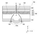
- FIG. 1 is a cross-sectional view of a laser device 100 according to this embodiment
- FIG. 2 is a schematic diagram showing the disassembled laser device 100.
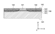
- the laser device 100 includes a first semiconductor layer 101, a second semiconductor layer 102, an active layer 103, a first light reflecting layer 104, a second light reflecting layer 105, a first electrode 106 and a second semiconductor layer 106.
- An electrode 107 is provided.
- the first semiconductor layer 101 , the second semiconductor layer 102 and the active layer 103 are collectively referred to as a laminate 150 .
- Each of these layers has a layer surface direction along the XY plane, and includes a first electrode 106, a first light reflecting layer 104, a first semiconductor layer 101, an active layer 103, a second semiconductor layer 102, and a second electrode 107. and the second light reflecting layer 105 are laminated in this order. Therefore, the laminate 150 is arranged between the first light reflecting layer 104 and the second light reflecting layer 105 .
- the first semiconductor layer 101 is a layer made of a semiconductor having a first conductivity type and transporting carriers to the active layer 103 .
- the first conductivity type can be n-type, and the first semiconductor layer 101 can be, for example, an n-GaN substrate.
- a lens 160 is provided on the first semiconductor layer 101 . This lens 160 will be described later.
- the second semiconductor layer 102 is made of a semiconductor of the second conductivity type and transports carriers to the active layer 103 .
- the second conductivity type can be p-type, and the second semiconductor layer 102 can be made of p-GaN, for example.
- the active layer 103 is arranged between the first semiconductor layer 101 and the second semiconductor layer 102 and is a layer that emits light by carrier recombination.
- the active layer 103 has a multi-quantum well structure in which multiple layers of quantum well layers and barrier layers are alternately laminated.
- the quantum well layers can be made of, for example, InGaN, and the barrier layers can be made of, for example, GaN.
- the active layer 103 may be any layer that emits light by carrier recombination.
- the surface on the first light reflecting layer 104 side is referred to as a first surface 151
- the surface on the second light reflecting layer 105 side is referred to as a second surface 152.
- Lens 160 is provided on first surface 151 .
- the first surface 151 has a main surface 151a and a lens surface 151b.
- the main surface 151a is a plane (XY plane) perpendicular to the optical axis direction (Z direction) of emitted light.
- the lens surface 151b is the surface of the lens 160 and is a surface that protrudes from the main surface 151a.
- the first light reflecting layer 104 reflects light of a specific wavelength (hereinafter referred to as wavelength ⁇ ) and transmits light of other wavelengths.
- the wavelength ⁇ is, for example, 445 nm.
- the first light reflecting layer 104 is a DBR (DBR ( Distributed Bragg Reflector).
- the first light reflecting layer 104 can have a laminated structure such as Ta 2 O 5 /SiO 2 , SiO 2 /SiN, SiO 2 /Nb 2 O 5 or the like.
- the first light reflecting layer 104 has a concave mirror 104c.
- the first light reflecting layer 104 is laminated on the first surface 151 of the laminate 150 with a constant thickness, and as shown in FIG.
- the surface opposite to the laminate 150 forms a convex surface 104e.
- a concave mirror 104c is formed on the first light reflecting layer 104. As shown in FIG.
- the second light reflecting layer 105 reflects light of wavelength ⁇ and transmits light of other wavelengths.
- the second light reflecting layer 105 is a DBR (DBR) made of a multilayer light reflecting film in which a plurality of high refractive index layers 105a and low refractive index layers 105b each having an optical film thickness of ⁇ /4 are alternately laminated.
- DBR DBR
- the second light reflecting layer 105 can have a laminated structure such as Ta 2 O 5 /SiO 2 , SiO 2 /SiN, SiO 2 /Nb 2 O 5 or the like.
- the first electrode 106 is provided around the concave mirror 104 c on the first light reflecting layer 104 and functions as one electrode of the laser element 100 .
- the first electrode 106 can be, for example, a single-layer metal film made of Au, Ni, Ti, or the like, or a multi-layer metal film made of Ti/Au, Ag/Pd, Ni/Au/Pt, or the like.
- the second electrode 107 is arranged between the second semiconductor layer 102 and the second light reflecting layer 105 and functions as the other electrode of the laser device 100 .
- the second electrode 107 is made of, for example, ITO (Indium Tin Oxide), ITiO (Indium Titan Oxide), TiO, AZO (Aluminum doped zinc oxide), ZnO, SnO, ZSnO, SnO 2 , SnO 3 , TiO, TiO 2 or graphene. It can be made of a transparent conductive material.
- the laminated body 150 has a current confinement structure.
- 3 and 4 are schematic diagrams showing current confinement structures.
- 3(a) and 4(a) are plan views of the current constriction structure viewed from the optical axis direction (Z direction).
- FIG. 3B is a cross-sectional view of the XZ cross section showing the current confinement structure
- FIG. 4B is a cross-sectional view of the YZ cross section showing the current confinement structure.
- the current confinement structure has a current injection region 121 and an insulating region 122 (dotted regions).
- the current injection region 121 is a region into which ions are not implanted (non-ion-implanted region) and has conductivity.
- the insulating region 122 is a region that surrounds the current injection region 121 in the layer surface direction (XY direction), and is a region (ion-implanted region) that is insulated by implanting ions into the semiconductor material forming the laminate 150 .
- the ions implanted into the insulating region 122 can be B (boron) ions.
- B ions ions such as O (oxygen) ions and H (hydrogen) ions that can insulate a semiconductor material may also be used.
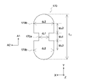
- the current injection region 121 is an elongated plane having one direction (Y direction) as its longitudinal direction and a direction perpendicular to the longitudinal direction (X direction) as its lateral direction. have a shape.
- the longitudinal direction (Y direction) of the current injection region 121 is defined as a first direction A1
- the lateral direction (X direction) of the current injection region 121 is defined as a second direction A2.
- Both the first direction A1 and the second direction A2 are directions orthogonal to the optical axis direction (Z direction) and mutually orthogonal.
- the length of the current injection region 121 along the first direction A1 is the length Le
- the width along the second direction A2 is the width de.
- the length L e is preferably 3 times or more the width d e , and more preferably 20 times or more.
- the length L e is preferably 40 ⁇ m or more.
- the current flowing through the laser element 100 cannot pass through the insulating region 122 and is concentrated in the current injection region 121. That is, the current injection region 121 and the insulating region 122 form a current confinement structure.
- the insulating region 122 may not be provided in all of the first semiconductor layer 101, the active layer 103, and the second semiconductor layer 102, and may be provided in at least one of these layers. Just do it.
- the planar shape of the current injection region 121 seen from the optical axis direction (Z direction) shown in FIGS. 3A and 4A is as shown in FIGS. 3B and 4B. , and a plan view of a portion of the current injection region 121 having the smallest diameter in the layer surface direction (XY direction). Since the diameter of the current injection region 121 increases with increasing distance from the interface between the second semiconductor layer 102 and the second electrode 106, the planar shape of the current injection region 121 is the shape of the current injection region 121 at the same interface.
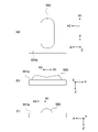
- FIGS. 5 to 7 are schematic diagrams showing the shape of the lens 160.
- FIG. 5A is a plan view of the first semiconductor layer 101 viewed from the optical axis direction (Z direction), and FIG. 5B is a cross-sectional view of the first semiconductor layer 101.
- FIG. FIG. 6 is a perspective view of the lens 160.
- FIG. 7A is a plan view of the lens 160 viewed from the X direction
- FIG. 7B is a plan view of the lens 160 viewed from the Y direction.
- the lens 160 is provided so as to protrude from the main surface 151a parallel to the XY plane toward the first light reflecting layer 104 side.
- the main surface 151a is referred to as a “flat surface” for defining the shape of the lens 160.
- FIG. 5A is a plan view of the first semiconductor layer 101 viewed from the optical axis direction (Z direction)
- FIG. 5B is a cross-sectional view of the first semiconductor layer 101.
- FIG. FIG. 6
- the lens 160 has an elongated lens shape with one direction (Y direction) parallel to the main surface 151a as the longitudinal direction and the transverse direction (X direction) perpendicular to the longitudinal direction.
- the longitudinal direction (Y direction) of the lens 160 coincides with the first direction A1, which is the longitudinal direction of the current injection region 121 (see FIG. 3). It coincides with the second direction A2, which is the lateral direction. That is, the lens 160 has a longitudinal direction in the first direction A1 and a lateral direction in the second direction A2.
- FIG. 8 is a schematic diagram showing the shape of the lens 160 viewed from the optical axis direction (Z direction).
- lens 160 has a central portion 160a and a non-central portion 160b.
- the center portion 160a is a portion of the lens 160 located at the center in the first direction A1.
- the width of the central portion 160a along the second direction A2 is a first width ds1
- the first width ds1 is the minimum width of the lens 160 along the second direction A2.
- the first width d s 1 can be, for example, 36 ⁇ m.
- the non-central portion 160b is a portion of the lens 160 located away from the central portion 160a in the first direction A1, and is a portion near both ends of the lens 160. As shown in FIG. Assuming that the width of the non-central portion 160b along the second direction A2 is a second width ds2 , the second width ds2 is the maximum width of the lens 160 along the second direction A2.
- the second width d s 2 is preferably 10 ⁇ m or more, and can be 40 ⁇ m, for example.
- a portion of the lens 160 between the central portion 160a and the non-central portion 160b has a shape in which the width along the second direction A2 gradually decreases from the non-central portion 160b toward the central portion 160a, as shown in FIG. can do.
- An angle ⁇ formed between the peripheral edge of the lens 160 and the first direction A1 when viewed from the optical axis direction (Z direction) can be set to 3.8°, for example.
- the length of the lens 160 along the first direction A1 is the length Ls as shown in FIG. is preferred.
- the length L s can be, for example, 100 ⁇ m.
- FIGS. 9A and 9B are schematic diagrams showing the shapes of the central portion 160a and the non-central portion 160b.
- FIG. 9A is the cross-sectional shape of the central portion 160a taken along the XZ plane
- FIG. 9B is the non-central portion 160b.
- the cross-sectional shape by an XZ plane is shown.
- the central portion 160a and the non-central portion 160b can have a curved shape in the XZ cross section. Different curve shapes.
- the curve drawn by the peripheral edge in the XZ cross section has an intermediate shape between FIGS. 9(a) and 9(b).
- the height (Z direction) of the lens 160 from the main surface 151a is defined as a height Hs.
- both the central portion 160a and the non-central portion 160b have a height Hs.
- the portion between the central portion 160a and the non-central portion 160b also has a height H s and, as shown in FIG. 7, the lens 160 has a uniform height H s .
- the height Hs is preferably 10 nm or more.
- the lens 160 may have a shape in which the height of the central portion 160a from the main surface 151a is higher than the height of the end portion from the main surface 151a.
- the end portions are portions located near both ends of the lens 160a in the first direction A1, such as the non-central portion 160b.
- the lens 160 has a radius of curvature (ROC) R s in the second direction A2 at the top of the lens surface 152b (hereinafter referred to as the lens top).
- ROC radius of curvature
- FIGS. 9A and 9B the lens apex is indicated by a dashed line, and the curvature radius Rs of the lens apex in the second direction A2 is indicated.
- both the central portion 160a and the non-central portion 160b have the same radius of curvature R s at the lens apex.
- a portion between the central portion 160a and the non-central portion 160b also has a radius of curvature Rs
- the top of the lens 160 has a uniform radius of curvature Rs in the second direction A2.
- This radius of curvature R s is preferably equal to or greater than the cavity length of the laser device 100 .
- FIG. 10 is a schematic diagram showing the cavity length K of the laser device 100. As shown in FIG. As shown in the figure, the cavity length K of the laser device 100 is the distance between the concave mirror 104c and the second light reflecting layer 105. As shown in FIG.
- the curvature radius Rs is preferably equal to or longer than the resonator length K, and may be the same as the resonator length K or longer than the resonator length K. This is because if the radius of curvature Rs is less than the cavity length K, laser oscillation, which will be described later, may not occur.
- the cavity length K can be, for example, 25 ⁇ m, and the radius of curvature R s can be, for example, 44 ⁇ m.
- the lens 160 preferably has a surface precision (RMS: Root Mean Square) of 1.0 nm or less on the lens surface 152b. This is because optical loss occurs in the lens surface 152b when the surface precision (RMS) of the lens surface 152b exceeds 1.0 nm.
- Surface accuracy (RMS) can be set to 0.6 nm, for example.
- FIG. 11 is a schematic diagram showing the positional relationship between the lens 160 and the current injection region 121 (see FIG. 3), and is a diagram of the lens 160 and the current injection region 121 viewed from the optical axis direction (Z direction). As shown in the figure, the lens 160 is positioned and shaped so that the current injection region 121 overlaps the lens 160 when viewed from the same direction.
- FIG. 12 is a cross-sectional view showing the lens 160 bonded to the first semiconductor layer 101. As shown in FIG. As shown in the figure, the lens 160 may be a member bonded to the first semiconductor layer 101 .
- the main surface 151a parallel to the XY plane is defined as a "plane" for defining the shape of the lens 160, but the main surface 151a is not limited to a flat surface parallel to the XY plane. It may be a curved surface or the like. In this case, a virtual plane parallel to the XY plane can be used as a “plane” for defining the shape of lens 160 .
- the lens 160 can have a shape in which the peripheral edge in the XZ cross section draws a curve as described above.
- the shape described by the periphery of the lens 160 in the XZ cross section can be configured as a partial circle, a partial parabola, a partial sine curve, a partial ellipse, or a partial catenary curve. This shape may not be strictly part of a circle, may not be strictly part of a parabola, may not be strictly part of a sine curve, or may not be strictly part of a sine curve. It may not be part of an ellipse, or strictly part of a catenary curve.
- the shape is part of a circle, part of a parabola, part of a sine curve, when it is generally a part of an ellipse, and when it is generally a part of a catenary curve.
- the shape is part of a circle, part of a parabola, part of a sine curve, part of an ellipse, part of a generally catenary curve.
- Some of these curves may be replaced with line segments.
- the shape drawn by the peripheral edge of the lens 160 in the XZ cross section can be obtained by measuring the shape of the lens surface 152b with a measuring instrument and analyzing the obtained data based on the method of least squares.
- FIG. A current flows between the first electrode 106 and the second electrode 107 when a voltage is applied between the first electrode 106 and the second electrode 107 .
- the current is confined by the current confinement structure and injected into the current injection region 121 as indicated by arrow C in FIG.
- This injected current causes spontaneous emission light F near the current injection region 121 of the active layer 103 .
- the spontaneous emission light F travels in the stacking direction (Z direction) of the laser element 100 and is reflected by the first light reflecting layer 104 and the second light reflecting layer 105 .
- the first light reflecting layer 104 and the second light reflecting layer 105 are configured to reflect light having the oscillation wavelength ⁇ , the component of the spontaneous emission light having the oscillation wavelength ⁇ A standing wave is formed between the two light reflecting layers 105 and amplified by the active layer 103 .
- the injected current exceeds a threshold, the light forming the standing wave causes lasing.
- the laser light E thus generated passes through the second light reflecting layer 105 and is emitted from the laser element 100 with the Z direction as the optical axis direction.
- the current injection region 121 has an elongated planar shape extending along the first direction A1 (Y direction), and the lens 160 also has an elongated lens shape extending along the first direction A1 (see FIG. 11).
- the light confinement region by the current injection region 121 is expanded in the first direction A1, while the light confinement region by the current injection region 121 is expanded in the second direction A2.
- the optical confinement area can be limited. As a result, the width of the laser light E emitted from the laser element along the first direction A1 is increased, and the radiation angle of the laser light E along the Y direction can be reduced.
- the lens 160 causes light resonance not only in the stacking direction (Z direction) but also in the first direction A1 (Y direction).
- the coherence of the laser beam E can be improved.
- the laser element 100 can emit the laser light E with a large beam diameter and a narrow radiation angle because the current injection region 121 and the lens 160 have an elongated shape along the first direction A1. It works as a line light source that emits a linear beam.
- the laser element 100 has the lens 160 having a uniform height Hs from the main surface 151a and a uniform radius of curvature Rs in the second direction A2 of the top of the lens.
- 14A and 14B are schematic diagrams of the lens 560 shown from each direction for comparison.
- the lens 560 has an elongated lens shape with a longitudinal direction in the first direction A1 and a lateral direction in the second direction A2.
- the lens 560 has a shape in which the height from the plane 551a is uneven and the height in the central portion is low.
- the lens 560 has a non-uniform radius of curvature in the second direction A2 of the top of the lens.
- the lens When the lens has a shape that is long in one direction (especially 40 ⁇ m or more), the central part is depressed as shown in FIG. It can have a non-uniform shape. If the laser device 100 were to have a lens 560 instead of the lens 160, the height of the lens 560 would be non-uniform, especially the edge would be higher than the center.
- the resonator length K (see FIG. 10) is different. Therefore, different longitudinal modes (repeated states in the Z direction) are established at different locations in the laser element 100 .
- the lens 560 has a non-uniform curvature radius at the top of the lens, different transverse modes (repeated states in the XY directions) are established within the laser element 100 . Due to these causes, when the laser element 100 has the lens 560, uneven brightness of the laser light E occurs within the laser element 100, the light field within the laser element 100 does not become coherent, and the laser light E with a narrow radiation angle is emitted. cannot be ejected.
- the laser element 100 has a lens 160 having a uniform height H s and a uniform radius of curvature R s at the top of the lens. Therefore, by forming the current injection region 121 on the lens 160, a mode having both resonance in the optical axis direction (Z direction) and resonance in the longitudinal direction (Y direction) of the lens 160 is formed. A laser device 100 that emits light with high linearity can be realized. Further, since the radius of curvature R s of the laser device 100 is uniform, the transverse mode can be unified, and since the height H s is uniform, the longitudinal mode can be unified in some cases. As a result, the laser element 100 can realize a good line light source because the laser light E can be emitted without luminance unevenness.
- FIG. 15 to 21 are schematic diagrams showing the manufacturing method of the laser element 100.
- FIG. 15 as shown in FIG. 15, a laminate 150 is produced.
- the laminate 150 can be produced by laminating the active layer 103 and the second semiconductor layer 102 on the first semiconductor layer 101 (substrate).
- the active layer 103 and the second semiconductor layer 102 can be laminated by a metal organic-chemical vapor deposition (MOCVD) method or the like.
- MOCVD metal organic-chemical vapor deposition
- insulating regions 122 are formed.
- the insulating region 122 can be formed by implanting ions into the stacked body 150 from the second semiconductor layer 102 side.
- the current injection region 121 which is a region into which ions are not implanted, can be formed.
- FIG. 17 is a plan view showing the shape of the structure 170, and is a view of the structure 170 viewed from the optical axis direction (Z direction).
- the structural body 170 has an elongated shape with one direction (Y direction) as the longitudinal direction and the transverse direction (X direction) perpendicular to the longitudinal direction.
- the longitudinal direction (Y direction) of the structure 170 coincides with the first direction A1, which is the longitudinal direction of the current injection region 121 (see FIG.
- the lateral direction (X direction) of the structure 170 coincides with the current injection region.
- 121 coincides with the second direction A2, which is the lateral direction of 121. That is, the structure 170 has the longitudinal direction in the first direction A1 and the lateral direction in the second direction A2.
- FIG. 19 is a schematic diagram showing the shape of the structure 170 viewed from the optical axis direction (Z direction).
- structure 170 has a central portion 170a and a non-central portion 170b.
- the center portion 170a is a portion of the structure 170 located at the center in the first direction A1.
- the width of the central portion 170a along the second direction A2 is a first width dp1
- the first width dp1 is the minimum width of the structure 170 along the second direction A2.
- the first width d p 1 can be, for example, 36 ⁇ m.
- the non-central portion 170b is a portion of the structural body 170 that is located away from the central portion 170a in the first direction A1, and is a portion near both ends of the structural body 170. As shown in FIG. Assuming that the width of the non-central portion 170b along the second direction A2 is a second width dp2 , the second width dp2 is the maximum width of the structure 170 along the second direction A2.
- the second width d p 2 is preferably 10 ⁇ m or more, and can be 40 ⁇ m, for example.
- the portion between the central portion 170a and the non-central portion 170b in the structure 170 has a shape in which the width along the second direction A2 gradually decreases from the non-central portion 170b toward the central portion 170a.
- An angle ⁇ formed between the peripheral edge of the structure 170 and the first direction A1 viewed from the optical axis direction (Z direction) can be set to 3.8°, for example.
- the length Lp is preferably larger than the second width dp2 , and is 40 ⁇ m. The above is preferable.
- the length Lp can be, for example, 100 ⁇ m.
- the structure 170 is made of a fluid material that has fluidity at room temperature or in the heating process described later.
- the flowable material can be an organic material or SOG (silicon on glass) and can be a commercially available photoresist.
- the structure 170 can be formed by applying a fluid material to the first surface 151 with a certain thickness and patterning it.
- the application of the fluid material can be performed by spin coating, and the rotation speed of spin coating is 10 rpm or more, for example, 3000 rpm.
- Patterning can be performed by forming a mask having the planar shape of the structure 170 described above on the fluid material and performing etching using the mask.
- the etching may be wet etching or dry etching.
- Reactive ion etching RIE; Reactive Ion Etching
- Masks can be formed by photolithography, and exposure equipment can utilize aligners, steppers, or electron beam writers.
- the light source can use g-line, i-line, KrF laser or ArF laser.
- FIG. 20 is a schematic diagram showing a structure 175 in which the structure 170 is deformed by heat treatment.
- the shape of the structure 175 is the same as the shape of the lens 160 described above. That is, the width of the central portion of the structure 175 is equal to the first width d s 1 of the lens 160 (see FIG. 8), and the width of the non-central portion of the structure 175 is equal to the second width d s 2 of the lens 160 .
- the height of the structure 175 is uniform and equal to the height Hs of the lens 160, and the radius of curvature of the top of the structure 175 in the second direction A2 is equal to the radius of curvature R s .
- FIG. 21 is a schematic diagram showing this etching.
- An etchant is supplied to the first semiconductor layer 101 from the first surface 151 side, as indicated by an arrow in FIG. Thereby, the first semiconductor layer 101 is etched from the first surface 151 side to form the lens 160 .
- the lens 160 having the same shape as that of the structure 175 can be formed.
- the etching may be wet etching or dry etching, but anisotropic etching is preferable, and reactive ion etching may be used.
- the structure 175 may be used as the lens 160 .
- the lens 160 is formed of a member separate from the first semiconductor layer 101, as shown in FIG.
- the structural body 175 can be used as the lens 160 by forming the structural body 170 from a material having transparency to the light of the oscillation wavelength ⁇ .
- the lens 160 can be formed on the first surface 151 as described above (see FIG. 6). After that, the first light reflecting layer 104, the second light reflecting layer 105, the first electrode 106 and the second electrode 107 are respectively formed, and the laser element 100 shown in FIG. 1 can be manufactured. Each of these layers can be formed by a sputtering method, a vacuum deposition method, or the like. When laminating the first light reflecting layer 104 on the first semiconductor layer 101, since the lens 160 is provided on the first surface 151, a concave mirror 104c is formed. It should be noted that the second light reflecting layer 105 and the second electrode 107 can also be formed before forming the lens 160 .
- the structure 170 has a narrow central portion 170a (see FIG. 19), so that the height of the structure 175 and the radius of curvature of the top are made uniform. height and the radius of curvature of the top of the lens can be made uniform. If the structure 170 has a uniform width when viewed in the Z direction, the central portion becomes hollow due to the influence of surface tension and weight when the structure 175 is deformed (see FIG. 14), and the curvature radius of the central portion becomes growing. On the other hand, if the structure 170 has a narrow central portion 170a, surface tension acts to reduce the radius of curvature, and the height and radius of curvature of the top of the structure 175 can be made uniform. Become.
- etching is performed under the condition that the surface accuracy (RMS: Root Mean Square) of the structure 175 is lower than the surface accuracy (RMS) of the first semiconductor layer 101.
- surface precision (RMS) of the surface of the lens 160 can be made lower than before etching. Thereby, the scattering loss on the surface of the lens 160 can be suppressed and the performance of the resonator can be improved. As a result, it is possible to reduce the threshold value and power consumption of the laser device 100, and to improve the output structure, efficiency, and reliability.
- the laser device 100 can be manufactured as described above. It should be noted that the method for manufacturing the laser element 100 is not limited to that shown here, and it is also possible to manufacture the laser element 100 by other manufacturing methods.
- FIG. 22 is a schematic diagram showing another manufacturing method of the laser element 100.
- FIG. After forming the structure 170 (see FIG. 17) on the first surface 151, heat treatment (reflow) is performed with the first surface 151 facing vertically downward as shown in the figure. Since this prevents the height of the central portion of the structure 175 from becoming lower due to gravity, the height of the structure 175 can be made uniform or the central portion can be made higher than the ends.
- the lens 160 included in the laser element 100 may have the following configuration in addition to the configuration described above.
- 23 and 25 are plan views of lens 160 having other configurations, and are views of lens 160 viewed from the optical axis direction (Z direction).
- the lens 160 may have a shape in which the width along the second direction A2 decreases stepwise from the non-central portion 160b toward the central portion 160a.
- the height H s of the lens 160 and the radius of curvature R s (see FIG. 9) of the top of the lens in the second direction A2 are uniform. 10) can be longer, for example 44 ⁇ m.
- a first width d s 1 along the second direction A2 of the central portion 160a can be, for example, 36 ⁇ m
- a second width d s2 along the second direction A2 of the non-central portion 160b can be, for example, 40 ⁇ m
- the length Ls of the lens 160 along the first direction A1 is, for example, 100 ⁇ m
- the length M s1 of the portion having the first width ds1 along the first direction A1 is, for example, 10 ⁇ m
- the length M s 2 along the first direction A1 of the portion having s 2 can be, for example, 30 ⁇ m.
- FIG. 24 is a plan view of a structure 170 capable of forming this lens 160 shape.
- the structure 170 has a constant thickness from the first surface 151 (see FIG. 17), and as shown in the figure, the width along the second direction A2 is stepped from the non-central portion 160b toward the central portion 160a. It can be a shape that decreases in shape.
- a first width d p 1 along the second direction A2 of the central portion 170a may be, for example, 36 ⁇ m
- a second width d p 2 along the second direction A2 of the non-central portion 170b may be, for example, 40 ⁇ m
- the length L p of the structure 170 along the first direction A1 is, for example, 100 ⁇ m
- the length M p 1 of the portion having the first width d p1 along the first direction A1 is, for example, 10 ⁇ m
- the second width The length M p 2 along the first direction A1 of the portion having d p 2 can be, for example, 30 ⁇ m.
- the lens 160 can also be formed in a shape in which rectangular blocks (B1 to B5) whose width narrows from the non-central portion 160b toward the central portion 160a are connected.
- the number of blocks is not particularly limited, and may be five, for example.
- the height H s of the lens 160 and the radius of curvature R s (see FIG. 9) of the top of the lens in the second direction A2 are uniform. 10) can be longer, for example 44 ⁇ m.
- a first width d s 1 along the second direction A2 of the central portion 160a can be, for example, 36 ⁇ m
- a second width d s2 along the second direction A2 of the non-central portion 160b can be, for example, 40 ⁇ m.
- a portion between the central portion 160a and the non-central portion 160b has a narrower width along the second direction A2 from the non-central portion 160b toward the central portion 160a. The relationship of fourth width d s 4>first width d s 1 is satisfied.
- the second width ds2 can be 40 ⁇ m
- the third width ds3 can be 39 ⁇ m
- the fourth width ds4 can be 38 ⁇ m
- the first width ds1 can be 36 ⁇ m.
- the length L s of the lens 160 along the first direction A1 is, for example, 100 ⁇ m
- the lengths M s 1 to M s 4 of each portion along the first direction A1 are 10 ⁇ m
- the length M s 2 is 10 ⁇ m.
- the length M s 3 may be 10 ⁇ m
- the length M s 4 may be 5 ⁇ m
- the length M s 1 may be 10 ⁇ m.
- FIG. 26 is a plan view of a structure 170 capable of forming this lens 160 shape.
- the structure 170 has a constant thickness from the first surface 151 (see FIG. 17), and as shown in the figure, rectangular blocks (B1 to B5 ) can be formed in a row.
- a first width d p 1 along the second direction A2 of the central portion 170a may be, for example, 36 ⁇ m
- a second width d p 2 along the second direction A2 of the non-central portion 170b may be, for example, 40 ⁇ m.
- the relation of fourth width d p 4>first width d p 1 is satisfied.
- the second width d p 2 can be 40 ⁇ m
- the third width d p 3 can be 39 ⁇ m
- the fourth width d p 4 can be 38 ⁇ m
- the first width d p 1 can be 36 ⁇ m.
- the length L p of the lens 160 along the first direction A1 is, for example, 100 ⁇ m, and the lengths M p 1 to M p 4 of each portion along the first direction A1 are 10 ⁇ m, and the length M p 2 is 10 ⁇ m.
- the length M p 3 may be 10 ⁇ m, the length M p 4 may be 5 ⁇ m, and the length M p 1 may be 10 ⁇ m.
- the lens 160 has the configuration shown in FIGS. 23 and 25, the height H s and the radius of curvature R s of the top of the lens are uniform, so that a good line light source that emits the laser light E without unevenness in brightness can be obtained. It is possible to realize In addition, the shape of the lens 160 may have a central portion 160a and a non-central portion 160b, and the height Hs and the radius of curvature Rs of the top portion of the lens may be uniform other than those shown here.
- FIG. 27 is a cross-sectional view of laser device 100 having wavelength conversion layer 181 .
- the wavelength conversion layer 181 is made of a wavelength conversion material, is provided on the side opposite to the laminate 150 of the second light reflection layer 105, and converts the wavelength of the laser light E (see FIG. 13) incident from the second light reflection layer 105. do.
- the wavelength conversion material forming the wavelength conversion layer 181 can be a wavelength conversion material that is excited by blue light and emits red light.
- red-emitting phosphor particles more specifically, (ME:Eu)S [where "ME” means at least one atom selected from the group consisting of Ca, Sr and Ba and the same applies hereinafter], (M:Sm)x(Si,Al) 12 (O,N) 16 [wherein "M” is at least one selected from the group consisting of Li, Mg and Ca , ME 2 Si 5 N 8 :Eu, (Ca:Eu)SiN 2 , (Ca:Eu)AlSiN 3 .
- the wavelength conversion material forming the wavelength conversion layer 181 can be a wavelength conversion material that emits green light when excited by blue light.
- green-emitting phosphor particles more specifically (ME:Eu)Ga 2 S 4 , (M:RE) X (Si, Al) 12 (O, N) 16 [however, “RE means Tb and Yb], (M:Tb) X (Si,Al) 12 (O,N) 16 , (M:Yb) X (Si,Al) 12 (O,N) 16 , Si 6- ZAlZOZN8 -Z : Eu can be mentioned.
- the wavelength conversion material forming the wavelength conversion layer 181 can be a wavelength conversion material that emits yellow light when excited by blue light. Specifically, yellow-emitting phosphor particles, more specifically, YAG (yttrium-aluminum-garnet)-based phosphor particles can be used.
- the wavelength conversion material may be of one type, or two or more types may be mixed and used.
- wavelength conversion layer 181 by using a mixture of two or more kinds of wavelength conversion materials constituting the wavelength conversion layer 181, it is also possible to adopt a configuration in which emitted light of a color other than yellow, green, and red is emitted from the wavelength conversion material mixture. can. Specifically, for example, it may be configured to emit cyan light .
- the wavelength conversion material forming the wavelength conversion layer 181 can be a wavelength conversion material that emits red light when excited by ultraviolet rays. Specifically, red-emitting phosphor particles, more specifically Y2O3:Eu, YVO4 :Eu, Y ( P , V) O4 :Eu, 3.5MgO.0.5MgF2.Ge 2 : Mn, CaSiO3: Pb, Mn, Mg6AsO11 : Mn, ( Sr, Mg) 3 ( PO4 ) 3 : Sn, La2O2S : Eu , Y2O2S : Eu can be done.
- the wavelength conversion material forming the wavelength conversion layer 181 can be a wavelength conversion material that emits green light when excited by ultraviolet rays.
- green - emitting phosphor particles more specifically LaPO4 :Ce,Tb, BaMgAl10O17 : Eu ,Mn, Zn2SiO4 :Mn, MgAl11O19 :Ce, Tb , Y 2 SiO 5 : Ce, Tb, MgAl 11 O 19 : CE, Tb, Mn, Si 6-Z Al ZO Z N 8-Z : Eu.
- the wavelength conversion material forming the wavelength conversion layer 181 can be a wavelength conversion material that emits blue light when excited by ultraviolet light.
- blue - emitting phosphor particles more specifically, BaMgAl10O17 :Eu, BaMg2Al16O27 :Eu, Sr2P2O7 : Eu , Sr5 ( PO4 ) 3Cl : Eu, (Sr, Ca, Ba, Mg) 5 (PO 4 ) 3 Cl:Eu, CaWO4, CaWO 4 :Pb.
- the wavelength conversion material that constitutes the wavelength conversion layer 181 can be a wavelength conversion material that emits yellow light when excited by ultraviolet light.
- yellow light-emitting phosphor particles more specifically, YAG-based phosphor particles can be mentioned.
- the wavelength conversion material may be of one type, or two or more types may be mixed and used.
- it is also possible to adopt a configuration in which emitted light of a color other than yellow, green, and red is emitted from the wavelength conversion material mixture.
- it may be configured to emit cyan light, and in this case, a mixture of the above-mentioned green light-emitting phosphor particles and blue light-emitting phosphor particles may be used.
- the wavelength conversion material is not limited to phosphor particles.
- quantum dots can be mentioned as described above.
- the size (diameter) of the quantum dot decreases, the bandgap energy increases and the wavelength of light emitted from the quantum dot decreases. That is, the smaller the size of the quantum dot, the shorter the wavelength of light (blue light), and the larger the size of the quantum dot, the longer the wavelength of light (red light). Therefore, by using the same material for the quantum dots and adjusting the size of the quantum dots, it is possible to obtain quantum dots that emit light of a desired wavelength (convert to a desired color).
- the quantum dots preferably have a core-shell structure.
- materials constituting quantum dots include Si ; , AgInS 2 , AgInSe 2 ; perovskite materials; III-V group compounds GaAs, GaP, InP, InAs, InGaAs, AlGaAs, InGaP, AlGaInP, InGaAsP, GaN; CdSe, CdSeS, CdS, CdTe, In 2 Se 3 , In 2 S 3 , Bi 2 Se 3 , Bi 2 S 3 , ZnSe, ZnTe, ZnS, HgTe, HgS, PbSe, PbS, TiO 2 and the like, but not limited thereto.
- the first semiconductor layer 101 is made of an n-type semiconductor material
- the second semiconductor layer 102 is made of a p-type semiconductor material.
- the semiconductor layer 102 may be made of an n-type semiconductor material.
- the laser device 100 may have other configurations that enable the operation of the laser device 100 described above.
- a laser element array can be configured by the laser elements 100 .
- FIG. 28 is a cross-sectional view of the laser element array 10 according to this embodiment, and
- FIG. 29 is a schematic plan view of the laser element array 10. As shown in FIG.
- the laser element array 10 is composed of a plurality of laser elements 100 arranged. Although the number of laser elements 100 constituting the laser element array 10 is not specified, it can be ten, for example. As shown in FIG. 29, the laser elements 100 can be arranged such that the first direction A1 (longitudinal direction of the lens 160) of each laser element 100 is aligned. The array pitch R (interval between the centers of the lenses 160) can be set to 20 ⁇ m, for example. The arrangement direction of the laser elements 100 is not limited to this, and the lenses 160 may be arranged in a hexagonal close-packed arrangement.
- each laser element 100 is separated from the first electrodes 106 of adjacent laser elements 100 . Therefore, by independently controlling the voltage between the first electrode 106 and the second electrode 107 of each laser element 100, each laser element 100 can be caused to emit light independently.
- the laser element array 10 is a good line light source in which each laser element 100 emits a laser beam E without luminance unevenness, and the output can be increased by arraying. For example, the output can exceed 1 W. be.
- the laser elements 100 can be provided with the wavelength conversion layer 181 .
- FIG. 30 is a cross-sectional view showing the laser element array 10 having the wavelength conversion layer 181. As shown in FIG.
- the wavelength conversion layer 181 may be provided in each laser element 100, or may be one continuous layer between a plurality of laser elements 100.
- the laser device according to this embodiment differs from the laser device according to the first embodiment mainly in the current confinement structure.
- the laser device according to this embodiment has a structure similar to that of the VCSEL device, but differs from the VCSEL device in that the laser device according to this embodiment causes resonance not only in the Z direction but also in another direction (Y direction). differ.
- FIG. 31 is a cross-sectional view of a laser device 200 according to this embodiment
- FIG. 32 is a cross-sectional view showing a partial exploded configuration of the laser device 200.
- the laser device 200 includes a substrate 201, a first semiconductor layer 202, a second semiconductor layer 203, a third semiconductor layer 204, an active layer 205, a tunnel junction layer 206, a first light reflecting layer 207, A second light reflecting layer 208 , a first electrode 209 , a second electrode 210 and an insulating film 211 are provided.
- the substrate 201 , the first semiconductor layer 202 , the second semiconductor layer 203 , the third semiconductor layer 204 , the active layer 205 and the tunnel junction layer 206 are collectively referred to as a laminate 250 .
- Each of these layers has a layer surface direction along the XY plane, and includes a first light reflecting layer 207, a substrate 201, a first semiconductor layer 202, an active layer 205, a second semiconductor layer 203, a third semiconductor layer 204,
- the layers are stacked in the order of the second light reflecting layer 208 . Therefore, the stack 250 is arranged between the first light reflecting layer 207 and the second light reflecting layer 208 .
- a substrate 201 supports each layer of the laser element 200 .
- Substrate 201 may be, for example, a semi-insulating InP substrate. As shown in FIG. 32, the substrate 201 is provided with a lens 260 . This lens 260 will be described later.
- the first semiconductor layer 202 is a layer made of a semiconductor having a first conductivity type and transporting carriers to the active layer 205 .
- the first conductivity type can be n-type, and the first semiconductor layer 202 can be a layer made of n-InP, for example.
- the second semiconductor layer 203 is made of a semiconductor of the second conductivity type and transports carriers to the active layer 205 .
- the second conductivity type can be p-type, and the second semiconductor layer 203 can be a layer made of p-InP, for example.
- the third semiconductor layer 204 is a layer made of a semiconductor having the first conductivity type and transporting carriers to the tunnel junction layer 206 .
- the third semiconductor layer 204 can be, for example, a layer made of n-InP.
- the active layer 205 is arranged between the first semiconductor layer 202 and the second semiconductor layer 203 and is a layer that emits light by carrier recombination.
- the active layer 205 has a multi-quantum well structure in which multiple layers of quantum well layers and barrier layers are alternately laminated.
- the quantum well layers are made of, for example, InGaAsP
- the barrier layers are made of, for example, InGaAsP having a composition different from that of the quantum well layers. can be made.
- the active layer 205 may be any layer that emits light by carrier recombination.
- Tunnel junction layer 206 forms a buried tunnel junction.
- the tunnel junction layer 206 is arranged between the central portion of the second semiconductor layer 203 and the central portion of the third semiconductor layer 204 .
- the tunnel junction layer 206 has a first layer 206a on the second semiconductor layer 203 side and a second layer 206b on the third semiconductor layer 204 side.
- the first layer 206a is a layer of the second conductivity type with a high impurity concentration, and can be made of, for example, p + -AlInGaAs.
- the second layer 206b is a layer of the first conductivity type with a high impurity concentration, and can be made of, for example, n + -InP.
- the active layer 205, the second semiconductor layer 203 and the third semiconductor layer 204 are removed at their outer peripheral portions to form a mesa (plateau structure) M.
- the tunnel junction layer 206 is arranged so as to be positioned in the center of the mesa M when viewed in the Z direction.
- the surface on the first light reflecting layer 207 side is defined as a first surface 251
- the surface on the second light reflecting layer 208 side is defined as a second surface 252 .
- a lens 260 is provided on the first surface 251 .
- the first surface 251 has a main surface 251a and a lens surface 251b.
- the main surface 251a is a plane (XY plane) perpendicular to the optical axis direction (Z direction) of emitted light.
- the lens surface 251b is the surface of the lens 260 and is a surface that protrudes from the main surface 251a.
- the first light reflecting layer 207 reflects light of a specific wavelength (hereinafter referred to as wavelength ⁇ ) and transmits light of other wavelengths.
- the wavelength ⁇ is, for example, a specific wavelength within 1300-1600 nm.
- the first light reflecting layer 207 is a DBR (DBR) made of a multilayer light reflecting film in which a plurality of high refractive index layers 207a and low refractive index layers 207b each having an optical film thickness of ⁇ /4 are alternately laminated.
- DBR DBR
- the first light reflecting layer 207 can have a laminated structure such as Ta 2 O 5 /SiO 2 , SiO 2 /SiN, SiO 2 /Nb 2 O 5 or the like.
- the first light reflecting layer 207 has a concave mirror 207c.
- the first light reflecting layer 207 is laminated on the second surface 201b of the substrate 201 with a constant thickness, and the surface on the side of the laminated body 250 forms a concave surface 207d according to the shape of the lens 260 provided on the first surface 251, The surface opposite the laminate 250 forms a convex surface 207e.
- a concave mirror 207c is formed on the first light reflecting layer 207. As shown in FIG.
- the second light reflecting layer 208 reflects light of wavelength ⁇ and transmits light of other wavelengths.
- the second light reflecting layer 208 is a multilayer light reflecting film DBR ( Distributed Bragg Reflector).
- the second light reflecting layer 208 can have a laminated structure such as Ta 2 O 5 /SiO 2 , SiO 2 /SiN, SiO 2 /Nb 2 O 5 or the like.
- the first electrode 209 is provided around the mesa M on the first semiconductor layer 202 and functions as one electrode of the laser element 200 .
- the first electrode 209 can be, for example, a single-layer metal film made of Au, Ni, or Ti, or a multi-layer metal film made of Ti/Au, Ag/Pd, Ni/Au/Pt, or the like.
- the second electrode 210 is provided around the second light reflecting layer 208 on the third semiconductor layer 204 and functions as the other electrode of the laser element 200 .
- the second electrode 210 can be, for example, a single-layer metal film made of Au, Ni, or Ti, or a multi-layer metal film made of Ti/Au, Ag/Pd, Ni/Au/Pt, or the like.
- the insulating film 211 is provided around the second electrode 210 on the side surface of the mesa M and the upper surface of the mesa M, and insulates the outer circumference of the mesa M. As shown in FIG.
- the insulating film 211 is made of any insulating material.
- FIG. 33 is a schematic diagram showing a current confinement structure.
- the current confinement structure has a current injection region 221 and an insulating region 222 as shown in the figure.
- a current injection region 221 is a region (tunnel junction region) in which a tunnel junction is formed by the tunnel junction layer 206, and current is passed through the tunnel junction.
- the insulating region 222 surrounds the current injection region 221 in the layer surface direction (XY direction) and is a region (non-tunnel junction region) that does not pass current because no tunnel junction is formed.
- the current flowing through the laser element 200 concentrates in the current injection region 221 because it cannot pass through the insulating region 222 . That is, the current injection region 221 and the insulating region 222 form a current confinement structure.
- the shape of the current injection region 221 in the laser device 200 is the same as the current injection region 121 according to the first embodiment. That is, the current injection region 221 has an elongated planar shape with the first direction A1 as the longitudinal direction and the second direction A2 as the lateral direction (see FIGS. 3 and 4). Both the first direction A1 and the second direction A2 are directions orthogonal to the optical axis direction (Z direction) and mutually orthogonal.
- the shape of the lens 260 in the laser element 200 is the same as the lens 160 according to the first embodiment. That is, the lens 260 has an elongated lens shape with the longitudinal direction in the first direction A1 and the lateral direction in the second direction A2. The length, width, height, radius of curvature of the top of the lens, and surface accuracy (RMS) of the lens 260 are also the same as those of the lens 160 .
- the lens 260 may be formed of a part of the substrate 201 as shown in FIG. (See FIG. 12).
- the laser device 200 operates similarly to the laser device 100 according to the first embodiment. That is, when a voltage is applied between the first electrode 209 and the second electrode 210 , current flows between the first electrode 209 and the second electrode 210 . The current is confined by the current confinement structure and injected into the current injection region 221 . The spontaneous emission light generated by this injected current is reflected by the first light reflecting layer 207 and the second light reflecting layer 208 to generate laser oscillation. The laser light generated thereby passes through the second light reflecting layer 208 and is emitted from the laser element 200 with the Z direction as the optical axis direction.
- the laser element 200 can emit laser light E with a large beam diameter and a narrow radiation angle due to the shapes of the current injection region 221 and the lens 260, and operates as a line light source that emits a linear beam.
- the laser element 200 also has a lens 260 in which the height H s from the main surface 251a and the radius of curvature R s (see FIG. 9) of the top of the lens in the second direction A2 are uniform. Therefore, by forming the current injection region 221 on the lens 260, a mode having both resonance in the optical axis direction (Z direction) and resonance in the longitudinal direction (Y direction) of the lens 260 is formed. A laser device 200 that emits light with high linearity can be realized. Further, in the laser device 200, since the radius of curvature R s is uniform, the transverse mode can be unified, and since the height H s is uniform, the longitudinal mode can be unified in some cases. As a result, the laser element 200 can realize a good line light source because the laser light E can be emitted without luminance unevenness. In addition, the lens 260 has a more uniform height and distributes stress, which can improve durability.
- Method for manufacturing laser element In the method of manufacturing the laser element 200, after layers up to the second layer 206b are laminated on the substrate 201 by the metal-organic chemical vapor deposition method or the like, the first layer 206a and the second layer 206b are removed by photolithography and etching. A portion is removed to form the tunnel junction layer 206 .
- the shape of the tunnel junction layer 206 can be freely controlled by photolithography.
- a third semiconductor layer 204 is laminated on the tunnel junction layer 206, and a mesa M is formed by photolithography and etching. Thereby, a laminate 250 is formed on the substrate 201 .
- the laser element 200 can be manufactured by providing the lens 260 on the substrate 201 and laminating the first light reflecting layer 207 and the second light reflecting layer 208 by the same method as in the first embodiment. Also, the laser element 200 can be manufactured by other manufacturing methods.
- the current confinement structure is provided by the buried tunnel junction of the tunnel junction layer 206.
- the current confinement structure may be provided by ion implantation into the tunnel junction layer 206 as follows. It is possible.
- FIG. 34 is a cross-sectional view of a laser device 200 having insulating regions 223 formed by ion implantation.
- the tunnel junction layer 206 is disposed entirely between the second semiconductor layer 203 and the third semiconductor layer 204, and the peripheral region of the tunnel junction layer 206 includes an insulating region 223 (dotted region). ) is provided.
- the current confinement structure is composed of a current injection region 221 and an insulating region 223, as shown in FIG.
- the current injection region 221 is formed by the tunnel junction layer 206 into which ions are not implanted.
- the insulating region 223 surrounds the current injection region 221 in the layer plane direction (XY direction) and is a region insulated by implanting ions into the tunnel junction layer 206 .
- the ions implanted into the ion implantation region can be B (boron) ions.
- ions such as O (oxygen) ions and H (hydrogen) ions that can insulate a semiconductor material may also be used.
- the current flowing through the laser element 200 is concentrated in the current injection region 221 because it cannot pass through the insulating region 223 . That is, the current injection region 221 and the insulating region 223 form a current confinement structure.
- each layer is laminated on the substrate 201 to produce the laminated body 250, but the laminated body is formed by laminating each layer on another supporting substrate, removing the supporting substrate, and bonding it to the substrate 201. 250 can also be formed.
- the laser element 200 is provided with a wavelength conversion layer (see FIG. 27) for changing the wavelength of emitted light on the opposite side of the second light reflection layer 208 from the laminate 250, as in the first embodiment. is also possible.
- the first semiconductor layer 202 and the third semiconductor layer 204 are made of an n-type semiconductor material
- the second semiconductor layer 203 is made of a p-type semiconductor material. It may be made of a p-type semiconductor material and the second semiconductor layer 203 may be made of an n-type semiconductor material.
- the first layer 206a of the tunnel junction layer 206 can be an n-type layer with a high impurity concentration
- the second layer 206b can be a p-type layer with a high impurity concentration.
- the laser device 200 may have other configurations that enable the laser device 200 to operate.
- the laser elements 200 can be arrayed as in the first embodiment.
- the laser element array composed of the laser elements 200 is a good line light source in which each laser element 200 emits a laser beam E without brightness unevenness, and can be made into an array to achieve a high output, for example, an output exceeding 1 W. It is possible.
- a laser element array composed of laser elements 200 may be provided with a wavelength conversion layer (see FIG. 28).
- the laser device according to this embodiment differs from the laser device according to the first embodiment mainly in the current confinement structure.
- the laser device according to this embodiment has a structure similar to that of the VCSEL device, but differs from the VCSEL device in that the laser device according to this embodiment causes resonance not only in the Z direction but also in another direction (Y direction). differ.
- FIG. 35 is a cross-sectional view of a laser device 300 according to this embodiment
- FIG. 36 is a cross-sectional view showing a partial exploded configuration of the laser device 300.
- the laser device 300 includes a substrate 301, a first semiconductor layer 302, a second semiconductor layer 303, an active layer 304, an oxidized constricting layer 305, a first light reflecting layer 306 and a second light reflecting layer 307. , a first electrode 308 , a second electrode 309 and an insulating film 310 .
- the substrate 301 , the first semiconductor layer 302 , the second semiconductor layer 303 , the active layer 304 and the oxidized constricting layer 305 are collectively referred to as a laminate 350 .
- Each of these layers has a layer surface direction along the XY plane, and includes a first light reflecting layer 306, a substrate 301, a first semiconductor layer 302, an active layer 304, a second semiconductor layer 303, an oxidized constricting layer 305, a
- the two light reflecting layers 307 are laminated in this order. Therefore, the stack 350 is arranged between the first light reflecting layer 306 and the second light reflecting layer 307 .
- a substrate 301 supports each layer of the laser element 300 .
- Substrate 301 may be, for example, a semi-insulating GaAs substrate.
- the substrate 301 is provided with a lens 360 . This lens 360 will be described later.
- the first semiconductor layer 302 is a layer made of a semiconductor having a first conductivity type and transporting carriers to the active layer 304 .
- the first conductivity type can be n-type, and the first semiconductor layer 302 can be a layer made of n-GaAs, for example.
- the second semiconductor layer 303 is made of a semiconductor of the second conductivity type and transports carriers to the active layer 304 .
- the second conductivity type can be p-type, and the second semiconductor layer 303 can be a layer made of p-GaAs, for example.
- the active layer 304 is arranged between the first semiconductor layer 302 and the second semiconductor layer 303 and is a layer that emits light by carrier recombination.
- the active layer 304 has a multi-quantum well structure in which quantum well layers and barrier layers are alternately laminated.
- the quantum well layers can be made of GaAs, and the barrier layers can be made of AlGaAs.
- the active layer 304 may be any layer that emits light by carrier recombination.
- the oxidized confinement layer 305 forms a current confinement structure.
- the oxidized constricting layer 305 has an unoxidized region 305a where the semiconductor material is not oxidized and an oxidized region 305b where the semiconductor material is oxidized.
- the non-oxidized region 305a is made of a material of the second conductivity type with a high impurity concentration, such as p + -AlAs.
- the oxidized region 305b is made of a material obtained by oxidizing the constituent material of the non-oxidized region 305a, and can be made of AlAs oxide, for example.
- the surface on the first light reflecting layer 306 side is defined as a first surface 351
- the surface on the second light reflecting layer 307 side is defined as a second surface 352 .
- a lens 360 is provided on the first surface 351 .
- the first surface 351 has a main surface 351a and a lens surface 351b.
- the main surface 351a is a plane (XY plane) perpendicular to the optical axis direction (Z direction) of emitted light.
- the lens surface 351b is the surface of the lens 360 and is a surface that protrudes from the main surface 351a.
- the first light reflecting layer 306 reflects light of a specific wavelength (hereinafter referred to as wavelength ⁇ ) and transmits light of other wavelengths.
- the wavelength ⁇ is, for example, a specific wavelength within the range of 850-1400 nm.
- the first light reflecting layer 306 is a DBR (DBR) made of a multilayer light reflecting film in which a plurality of high refractive index layers 306a and low refractive index layers 306b each having an optical film thickness of ⁇ /4 are alternately laminated.
- DBR DBR
- the first light reflecting layer 306 can have a laminated structure such as Ta2O5 / SiO2 , SiO2 / SiN , or SiO2 / Nb2O5 .
- the first light reflecting layer 306 has a concave mirror 306c.
- the first light reflecting layer 306 is laminated on the second surface 301b of the substrate 301 with a constant thickness, and the surface on the side of the laminated body 350 forms a concave surface 306d according to the shape of the lens 360 provided on the first surface 351, The surface opposite the laminate 350 forms a convex surface 306e.
- a concave mirror 306c is formed on the first light reflecting layer 306. As shown in FIG.
- the second light reflecting layer 307 reflects light of wavelength ⁇ and transmits light of other wavelengths.
- the second light reflecting layer 307 is a multilayer light reflecting film DBR ( Distributed Bragg Reflector).
- the second light reflective layer 307 can be a semiconductor DBR made of a semiconductor material.
- the active layer 304, the second semiconductor layer 303, the oxidized constricting layer 305 and the second light reflecting layer 307 are removed at their outer peripheral portions to form a mesa (plateau structure) M.
- the first electrode 308 is provided around the mesa M on the first semiconductor layer 302 and functions as one electrode of the laser element 300 .
- the first electrode 308 can be, for example, a single-layer metal film made of Au, Ni, or Ti, or a multi-layer metal film made of Ti/Au, Ag/Pd, Ni/Au/Pt, or the like.
- a second electrode 309 is provided on the second light reflecting layer 307 and functions as the other electrode of the laser element 300 .
- the second electrode 309 can be, for example, a single-layer metal film made of Au, Ni, Ti, or the like, or a multi-layer metal film made of Ti/Au, Ag/Pd, Ni/Au/Pt, or the like.
- the insulating film 310 is provided around the second electrode 309 on the side surface of the mesa M and the upper surface of the mesa M, and insulates the outer periphery of the mesa M.
- the insulating film 310 is made of any insulating material.
- FIG. 37 is a schematic diagram showing a current confinement structure.
- the current confining structure has a current injection region 321 and an insulating region 322 as shown in the figure.
- the current injection region 321 is a region having conductivity due to the non-oxidized region 305a.
- the insulating region 322 surrounds the current injection region 221 in the layer plane direction (XY direction) and is a region that does not have conductivity due to the oxidized region 305b that is insulated by oxidation.
- the current flowing through the laser element 300 concentrates in the current injection region 321 because it cannot pass through the insulating region 322 . That is, in the laser element 300, the current confinement structure is formed by the oxidized confinement layer 305.
- the shape of the current injection region 321 in the laser device 300 is the same as the current injection region 321 according to the first embodiment. That is, the current injection region 321 has an elongated planar shape with the first direction A1 as the longitudinal direction and the second direction A2 as the lateral direction (see FIGS. 3 and 4). Both the first direction A1 and the second direction A2 are directions orthogonal to the optical axis direction (Z direction) and mutually orthogonal.
- the shape of the lens 360 in the laser element 300 is the same as the lens 160 according to the first embodiment. That is, the lens 360 has an elongated lens shape with the longitudinal direction in the first direction A1 and the lateral direction in the second direction A2. The length, width, height, radius of curvature of the top of the lens, and surface precision (RMS) of the lens 360 are also the same as those of the lens 160 .
- the lens 360 may be formed of a part of the substrate 301 as shown in FIG. (See FIG. 12).
- the laser device 300 operates similarly to the laser device 100 according to the first embodiment. That is, when a voltage is applied between the first electrode 308 and the second electrode 309 , current flows between the first electrode 308 and the second electrode 309 . A current is confined by the current confinement structure and injected into the current injection region 321 . The spontaneous emission light generated by this injected current is reflected by the first light reflecting layer 306 and the second light reflecting layer 307 to generate laser oscillation. The laser light generated thereby passes through the second light reflecting layer 307 and is emitted from the laser element 300 with the Z direction as the optical axis direction.
- the laser element 300 can emit laser light E with a large beam diameter and a narrow radiation angle due to the shapes of the current injection region 321 and the lens 360, and operates as a line light source that emits a linear beam.
- the laser element 300 also has a lens 360 in which the height H s from the main surface 351a and the radius of curvature R s (see FIG. 9) of the top of the lens in the second direction A2 are uniform. Therefore, by forming the current injection region 321 on the lens 360, a mode having both resonance in the optical axis direction (Z direction) and resonance in the longitudinal direction (Y direction) of the lens 360 is formed. A laser element 300 that emits light with high linearity can be realized. In the laser device 300, since the radius of curvature R s of the top of the lens is uniform, the transverse mode can be unified, and since the height H s is uniform, the longitudinal mode can be unified in some cases. be. As a result, the laser element 300 can realize a good line light source because the laser light E can be emitted without luminance unevenness. In addition, the lens 360 has a more uniform height and stress distribution, which can improve durability.
- the mesa M is formed by photolithography and etching.
- the material of the oxidized constricting layer 305 is oxidized from the outer peripheral side by a method such as heating the laminated body 350 in a water vapor atmosphere to form an oxidized region 305b.
- the shape of the non-oxidized region 305a viewed from the Z direction can be controlled by the shape of the mesa M viewed from the Z direction.
- the laser element 300 can be manufactured by providing the lens 360 on the substrate 301 and laminating the first light reflecting layer 306 and the second light reflecting layer 307 by the same method as in the first embodiment. Also, the laser device 300 can be manufactured by other manufacturing methods.
- each layer is laminated on the substrate 301 to produce the laminated body 350, but the laminated body is formed by laminating each layer on another supporting substrate, removing the supporting substrate, and bonding it to the substrate 301. It is also possible to form 350.
- the laser element 300 is provided with a wavelength conversion layer (see FIG. 27) for changing the wavelength of emitted light on the opposite side of the second light reflection layer 307 from the laminate 250, as in the first embodiment. is also possible.
- the first semiconductor layer 302 is made of an n-type semiconductor material and the second semiconductor layer 303 is made of a p-type semiconductor material
- the first semiconductor layer 302 is made of a p-type semiconductor material
- the second semiconductor layer 303 is made of a p-type semiconductor material.
- the non-oxidized region 305a of the oxidized constricting layer 305 can be made of an n-type material with a high impurity concentration.
- the laser device 300 may have other configurations that enable the operation of the laser device 300 to be realized.
- the laser elements 300 can be arrayed as in the first embodiment.
- the laser element array composed of the laser elements 300 is a good line light source in which each laser element 300 emits a laser beam E without luminance unevenness, and the output can be increased by arraying, for example, the output exceeds 1 W. It is possible.
- a laser element array composed of laser elements 300 may be provided with a wavelength conversion layer (see FIG. 28).
- the present technology can also have the following configuration. (1) a first light reflecting layer that reflects light of a specific wavelength; a second light reflecting layer that reflects light of the wavelength; a first semiconductor layer made of a semiconductor material having a first conductivity type; a second semiconductor layer made of a semiconductor material having a second conductivity type; and an active layer that is disposed between the first light reflecting layer and the second light reflecting layer and that emits light due to carrier recombination.
- the lens has a longitudinal direction in a first direction parallel to a plane perpendicular to the optical axis direction of emitted light, a lateral direction in a second direction parallel to the plane and orthogonal to the first direction, and 1, has a lens shape that protrudes toward the light reflecting layer side, has a first width that is the minimum width along the second direction at the central portion in the first direction, and The non-center portion has a second width that is the maximum width along the second direction, the height from the plane is uniform or the center portion is higher than the end portions, and the lens top portion has a second width.
- the first light reflecting layer is laminated on the first surface and forms a concave mirror having a concave shape on the lens.
- the laminate has a current confinement structure that confines current and forms a current injection region where current concentrates,
- the current injection region has a shape in which a planar figure viewed from the optical axis direction overlaps the lens when viewed from the optical axis direction, with the first direction being the longitudinal direction and the second direction being the lateral direction. a laser element.
- the laser device according to (1) or (2) above The length of the lens along the first direction is greater than the second width of the laser element.
- the laser device according to any one of (1) to (3) above, The laser element, wherein the length of the lens along the first direction is 40 ⁇ m or more.
- the laser device according to any one of (1) to (4) above, The laser element, wherein the second width of the lens is 10 ⁇ m or more.
- the cavity length of the laser element is the distance between the concave mirror and the second light reflecting layer, The laser device, wherein the radius of curvature is equal to or greater than the cavity length.
- the laser device according to any one of (1) to (6) above, The laser element, wherein the lens has a surface accuracy of 1.0 nm or less in RMS (Root Mean Square).
- the laser device according to any one of (1) to (11) above, The laser device, wherein the first light reflecting layer and the second reflecting layer are DBRs (Distributed Bragg Reflectors) made of multilayer light reflecting films.
- DBRs Distributed Bragg Reflectors
- the lens has a longitudinal direction in a first direction parallel to a plane perpendicular to the optical axis direction of emitted light, a lateral direction in a second direction parallel to the plane and orthogonal to the first direction, and 1, has a lens shape that protrudes toward the light reflecting layer side, has a first width that is the minimum width along the second direction at the central portion in the first direction, and The non-center portion has a second width that is the maximum width along the second direction, the height from the plane is uniform or the center portion is higher than the end portions, and the lens top portion has a second width.
- the first light reflecting layer is laminated on the first surface and forms a concave mirror having a concave shape on the lens.
- Laser element array (14) a first semiconductor layer made of a semiconductor material having a first conductivity type; a second semiconductor layer made of a semiconductor material having a second conductivity type; forming a stack having a first side and a second side, with an active layer disposed therebetween for emitting light by carrier recombination; Assuming that a direction parallel to a plane perpendicular to the optical axis direction of emitted light is a first direction and a direction parallel to the plane and perpendicular to the first direction is a second direction, , made of a fluid material, having a certain thickness, the first direction being the longitudinal direction, the second direction being the lateral direction, and the central portion in the first direction being along the second direction forming a structure having a first width that is the smallest width along the second direction, and a non-central portion in the first
- a method for manufacturing a laser device comprising: forming a second light reflecting layer that reflects light of the wavelength on the second surface side of the laminate.
- a method for manufacturing a laser device according to (14) above In the step of forming the lens, the structure has a lens shape protruding toward the first light reflecting layer, with the first direction being the longitudinal direction and the second direction being the lateral direction, The central part has the first width, the non-central part has the second width, the height from the plane is uniform or the central part is higher than the end parts, and the top part A method of manufacturing a laser device, wherein the shape is deformed into a shape having a uniform radius of curvature in the second direction. (16) A method for manufacturing a laser device according to (15) above, In the step of forming the lens, the layered body is etched using the structure deformed into the shape as an etching mask to form the lens on the first surface.
- a method for manufacturing a laser device according to (15) above In the step of forming the lens, the structure deformed into the shape is used as the lens.
- a method for manufacturing a laser device according to any one of (14) to (17) above The length of the structure along the first direction is greater than the second width of the laser element.
- (19) A method for manufacturing a laser device according to any one of (14) to (18) above, The laser element, wherein the structure has a length along the first direction of 40 ⁇ m or more.
- the etching is dry etching or wet etching. The laser device.
- Tunnel Bonding layer 305 Oxidation constricting layer 104, 207, 306 First light reflecting layer 104c, 207c, 306c Concave mirror 105, 208, 307 Second light reflecting layer 106, 209, 308 First electrode 107, 210, 309 Second electrode 121, 221, 321 Current injection region 122, 222, 322 Insulation region 150, 250, 350 Laminate 160, 260, 360 Lens 170, 270, 370 Structure 175, 275, 375 Structure 181... Wavelength conversion layer
Abstract
Description
上記第1の光反射層は、特定の波長の光を反射する。
上記第2の光反射層は、上記波長の光を反射する。
上記積層体は、第1の伝導型を有する半導体材料からなる第1の半導体層と、第2の伝導型を有する半導体材料からなる第2の半導体層と、上記第1の半導体層と上記第2の半導体層の間に配置され、キャリア再結合による発光を生じる活性層とを備え、上記第1の光反射層と上記第2の光反射層の間に配置され、上記第1の光反射層側の第1の面と、上記第2の光反射層側の第2の面を有し、上記第1の面にレンズが設けられている。
上記レンズは、出射光の光軸方向に垂直な平面に平行な第1の方向を長手方向、上記平面に平行かつ上記第1の方向に直交する第2の方向を短手方向とし、上記第1の光反射層側に突出するレンズ形状を有し、上記第1の方向における中央部が上記第2の方向に沿った最小幅である第1の幅を有し、上記第1の方向における非中央部が上記第2の方向に沿った最大幅である第2の幅を有し、上記平面からの高さが均一あるいは中央部が端部よりも高い形状であり、レンズ頂部の上記第2の方向における曲率半径が均一である。
上記第1の光反射層は、上記第1の面に積層され、上記レンズ上に凹面形状を有する凹面鏡を形成する。なお、本明細において高さや曲率半径が「均一」とは、所定の凹面鏡の頂部における平均値から、おおよそすべての部位においてその値が±20%を超えない範囲とする。
上記電流注入領域は、上記光軸方向から見た平面図形が上記第1の方向を長手方向、上記第2の方向を短手方向とし、上記光軸方向から見て上記レンズに重複する形状を有してもよい。
上記曲率半径は、上記共振器長以上であってもよい。
レーザ素子。
上記レーザ素子は、
特定の波長の光を反射する第1の光反射層と、
上記波長の光を反射する第2の光反射層と、
第1の伝導型を有する半導体材料からなる第1の半導体層と、第2の伝導型を有する半導体材料からなる第2の半導体層と、上記第1の半導体層と上記第2の半導体層の間に配置され、キャリア再結合による発光を生じる活性層とを備え、上記第1の光反射層と上記第2の光反射層の間に配置され、上記第1の光反射層側の第1の面と、上記第2の光反射層側の第2の面を有し、上記第1の面にレンズが設けられた積層体と
を具備し、
上記レンズは、出射光の光軸方向に垂直な平面に平行な第1の方向を長手方向、上記平面に平行かつ上記第1の方向に直交する第2の方向を短手方向とし、上記第1の光反射層側に突出するレンズ形状を有し、上記第1の方向における中央部が上記第2の方向に沿った最小幅である第1の幅を有し、上記第1の方向における非中央部が上記第2の方向に沿った最大幅である第2の幅を有し、上記平面からの高さが均一あるいは中央部が端部よりも高い形状であり、レンズ頂部の上記第2の方向における曲率半径が均一であり、
上記第1の光反射層は、上記第1の面に積層され、上記レンズ上に凹面形状を有する凹面鏡を形成する。
出射光の光軸方向に垂直な平面に平行な一方向を第1の方向とし、上記平面に平行かつ上記第1の方向に直交する方向を第2の方向とすると、上記第1の面に、流動性材料からなり、一定の厚みを有し、上記第1の方向を長手方向、上記第2の方向を短手方向とし、上記第1の方向における中央部が上記第2の方向に沿った最小幅である第1の幅を有し、上記第1の方向における非中央部が上記第2の方向に沿った最大幅である第2の幅を有する構造体を形成し、
上記構造体を加熱し、上記流動性材料を流動させて上記構造体を変形させ、上記構造体の形状を利用して上記第1の面に上記平面からの高さが均一あるいは中央部が端部よりも高い形状であり、レンズ頂部の上記第2の方向における曲率半径が均一であるレンズを形成し、
上記第1の面上に特定の波長の光を反射する第1の光反射層を積層し、上記レンズ上に凹面形状を有する凹面鏡を形成し、
上記積層体の上記第2の面側に上記波長の光を反射する第2の光反射層を形成する。
本技術の第1の実施形態に係るレーザ素子について説明する。本開示の各図において、レーザ素子から出射される光の光軸方向をZ方向とし、Z方向に直交する一方向をX方向、Z方向及びX方向に直交する方向をY方向とする。本実施形態に係るレーザ素子は、VCSEL(Vertical Cavity Surface Emitting Laser:垂直共振器型面発光レーザ)素子に類似した構造を有するが、VCSEL素子はZ方向において光の共振が生じる構造であるのに対し、本実施形態に係るレーザ素子はZ方向に加え、他の方向(Y方向)にも共振を生じる点でVCSEL素子とは相違する。
図1は本実施形態に係るレーザ素子100の断面図であり、図2はレーザ素子100を分解して示す模式図である。これらの図に示すように、レーザ素子100は、第1半導体層101、第2半導体層102、活性層103、第1光反射層104、第2光反射層105、第1電極106及び第2電極107を備える。このうち、第1半導体層101、第2半導体層102及び活性層103を併せて積層体150とする。
レンズ160の形状について説明する。図5乃至図7はレンズ160の形状を示す模式図である。図5(a)は、光軸方向(Z方向)から見た第1半導体層101の面図、図5(b)は第1半導体層101の断面図である。図6はレンズ160の斜視図である。図7(a)はX方向から見たレンズ160の平面図、図7(b)はY方向から見たレンズ160の平面図である。図5乃至図7に示すように、レンズ160は、X-Y平面に平行な主面151aから第1光反射層104側に突出して設けられている。以下、主面151aをレンズ160の形状を規定するための「平面」とする。
レーザ素子100の動作について説明する。図13は、レーザ素子100の動作を示す模式図である。第1電極106と第2電極107の間に電圧を印加すると、第1電極106と第2電極107の間に電流が流れる。電流は電流狭窄構造により狭窄され、図13に矢印Cとして示すように電流注入領域121に注入される。
上記のようにレーザ素子100は、主面151aからの高さHsが均一であり、レンズ頂部の第2方向A2における曲率半径Rsが均一であるレンズ160を有する。図14は比較として示すレンズ560を各方向から見た模式図である。レンズ560は、第1方向A1を長手方向とし、第2方向A2を短手方向とする細長いレンズ形状を有する。レンズ560は、平面551aからの高さが不均一であり、中央部の高さが低い形状を有する。また、レンズ560はレンズ頂部の第2方向A2における曲率半径も不均一である。
レーザ素子100の製造方法について説明する。図15乃至図21は、レーザ素子100の製造方法を示す模式図である。まず、図15に示すように積層体150を作製する。積層体150は、第1半導体層101(基板)上に活性層103及び第2半導体層102を積層して作製することができる。活性層103及び第2半導体層102は有機金属化学的気相成長(MOCVD;Metal Organic-Chemical Vapor Deposition)法等により積層することができる。
レーザ素子100が備えるレンズ160は、上記構成の他に以下に示す構成を有するものであってもよい。図23及び図25は、他の構成を有するレンズ160の平面図であり、レンズ160を光軸方向(Z方向)から見た図である。
レーザ素子100の構成は上述のものに限られず、波長変換層を備えるものとすることも可能である。図27は波長変換層181を備えるレーザ素子100の断面図である。波長変換層181は波長変換材料からなり、第2光反射層105の積層体150とは反対側に設けられ、第2光反射層105から入射するレーザ光E(図13参照)の波長を変換する。
レーザ素子100によってレーザ素子アレイを構成することが可能である。図28は本実施形態に係るレーザ素子アレイ10の断面図であり、図29はレーザ素子アレイ10の模式的平面図である。
本技術の第2の実施形態に係るレーザ素子について説明する。本実施形態に係るレーザ素子は、第1の実施形態に係るレーザ素子に対して主に電流狭窄構造が異なる。本実施形態に係るレーザ素子は、VCSEL素子に類似した構造を有するが、本実施形態に係るレーザ素子はZ方向に加え、他の方向(Y方向)にも共振を生じる点でVCSEL素子とは相違する。
図31は本実施形態に係るレーザ素子200の断面図であり、図32はレーザ素子200の一部構成を分解して示す断面図である。これらの図に示すように、レーザ素子200は、基板201、第1半導体層202、第2半導体層203、第3半導体層204、活性層205、トンネル接合層206、第1光反射層207、第2光反射層208、第1電極209、第2電極210及び絶縁膜211を備える。このうち、基板201、第1半導体層202、第2半導体層203、第3半導体層204、活性層205及びトンネル接合層206を併せて積層体250とする。
レーザ素子200における電流注入領域221の形状は第1の実施形態に係る電流注入領域121と同一である。即ち、電流注入領域221は、第1方向A1を長手方向、第2方向A2を短手方向とする細長い平面形状を有する(図3及び図4参照)。第1方向A1及び第2方向A2は共に光軸方向(Z方向)に直交し、かつ互いに直交する方向である。
レーザ素子200は第1の実施形態に係るレーザ素子100と同様に動作する。即ち、第1電極209と第2電極210の間に電圧を印加すると、第1電極209と第2電極210の間に電流が流れる。電流は電流狭窄構造により狭窄され、電流注入領域221に注入される。この注入電流によって生じた自然放出光は第1光反射層207及び第2光反射層208によって反射され、レーザ発振を生じる。これにより生じたレーザ光は、第2光反射層208を透過し、Z方向を光軸方向としてレーザ素子200から出射される。レーザ素子200では、電流注入領域221及びレンズ260の形状により、ビーム径が大きく、放射角の狭いレーザ光Eを出射することが可能であり、線状のビームを出射するライン光源として動作する。
レーザ素子200においても、主面251aからの高さHsとレンズ頂部の第2方向A2における曲率半径Rs(図9参照)が均一であるレンズ260を有している。このため、レンズ260上に電流注入領域221を形成することで、光軸方向(Z方向)への共振とレンズ260の長手方向(Y方向)への共振との両方を持つモードを形成し、直線性の高い光を出射するレーザ素子200を実現することができる。また、レーザ素子200では、曲率半径Rsが均一であるため、横モードを単一化することができ、高さHsが均一であるため、縦モードを単一化できる場合がある。これらによって、輝度ムラのないレーザ光Eを出射することができるため、レーザ素子200は良好なライン光源を実現することが可能である。さらに、レンズ260では高さがより均一であり、応力が分散されるため、耐久性を向上させることが可能である。
レーザ素子200の製造方法では、基板201上に第2層206bまでの各層を有機金属化学的気相成長法等により積層した後、フォトリソグラフィ及びエッチングにより第1層206a及び第2層206bの不要部分を除去し、トンネル接合層206を形成する。トンネル接合層206はフォトリソグラフィにより、自由に形状を制御することが可能である。
レーザ素子200では上記のように、トンネル接合層206による埋め込みトンネル接合によって電流狭窄構造が設けられるものとしたが、次のように、トンネル接合層206へのイオン注入によって電流狭窄構造を設けることも可能である。
上記説明では、基板201上に各層を積層し、積層体250を作製するものとしたが、他の支持基板上に各層を積層し、支持基板を除去して基板201に接合することによって積層体250を形成することも可能である。また、レーザ素子200は第1の実施形態と同様に、第2光反射層208の積層体250とは反対側に出射光の波長を変化する波長変換層(図27参照)を備えるものとすることも可能である。
レーザ素子200は第1の実施形態と同様にアレイ化することが可能である。レーザ素子200からなるレーザ素子アレイは、各レーザ素子200が輝度ムラのないレーザ光Eを出射する良好なライン光源であると共にアレイ化により高出力化が可能であり、例えば1Wを超える出力とすることが可能である。レーザ素子200からなるレーザ素子アレイは波長変換層(図28参照)を備えるものであってもよい。
本技術の第3の実施形態に係るレーザ素子について説明する。本実施形態に係るレーザ素子は、第1の実施形態に係るレーザ素子に対して主に電流狭窄構造が異なる。本実施形態に係るレーザ素子は、VCSEL素子に類似した構造を有するが、本実施形態に係るレーザ素子はZ方向に加え、他の方向(Y方向)にも共振を生じる点でVCSEL素子とは相違する。
図35は本実施形態に係るレーザ素子300の断面図であり、図36はレーザ素子300の一部構成を分解して示す断面図である。これらの図に示すように、レーザ素子300は、基板301、第1半導体層302、第2半導体層303、活性層304、酸化狭窄層305、第1光反射層306、第2光反射層307、第1電極308、第2電極309及び絶縁膜310を備える。このうち、基板301、第1半導体層302、第2半導体層303、活性層304及び酸化狭窄層305を併せて積層体350とする。
レーザ素子300における電流注入領域321の形状は第1の実施形態に係る電流注入領域321と同一である。即ち、電流注入領域321は、第1方向A1を長手方向、第2方向A2を短手方向とする細長い平面形状を有する(図3及び図4参照)。第1方向A1及び第2方向A2は共に光軸方向(Z方向)に直交し、かつ互いに直交する方向である。
レーザ素子300は第1の実施形態に係るレーザ素子100と同様に動作する。即ち、第1電極308と第2電極309の間に電圧を印加すると、第1電極308と第2電極309の間に電流が流れる。電流は電流狭窄構造により狭窄され、電流注入領域321に注入される。この注入電流によって生じた自然放出光は第1光反射層306及び第2光反射層307によって反射され、レーザ発振を生じる。これにより生じたレーザ光は、第2光反射層307を透過し、Z方向を光軸方向としてレーザ素子300から出射される。レーザ素子300では、電流注入領域321及びレンズ360の形状により、ビーム径が大きく、放射角の狭いレーザ光Eを出射することが可能であり、線状のビームを出射するライン光源として動作する。
レーザ素子300においても、主面351aからの高さHsとレンズ頂部の第2方向A2における曲率半径Rs(図9参照)が均一であるレンズ360を有している。このため、レンズ360上に電流注入領域321を形成することで、光軸方向(Z方向)への共振とレンズ360の長手方向(Y方向)への共振との両方を持つモードを形成し、直線性の高い光を出射するレーザ素子300を実現することができる。また、レーザ素子300では、レンズ頂部の曲率半径Rsが均一であるため、横モードを単一化することができ、高さHsが均一であるため、縦モードを単一化できる場合がある。これらによって、輝度ムラのないレーザ光Eを出射することができるため、レーザ素子300は良好なライン光源を実現することが可能である。さらに、レンズ360では高さがより均一であり、応力が分散されるため、耐久性を向上させることが可能である。
レーザ素子300の製造方法では、基板301上に第2光反射層307までの各層を、有機金属化学的気相成長法等によって積層した後、フォトリソグラフィ及びエッチングによりメサMを形成する。続いて、積層体350を水蒸気雰囲気下で加熱する等の方法で酸化狭窄層305の材料を外周側から酸化させ、酸化領域305bを形成する。この際、Z方向から見たメサMの形状によって、同方向から見た非酸化領域305aの形状を制御することができる。
上記説明では、基板301上に各層を積層し、積層体350を作製するものとしたが、他の支持基板上に各層を積層し、支持基板を除去して基板301に接合することによって積層体350を形成することも可能である。また、レーザ素子300は第1の実施形態と同様に、第2光反射層307の積層体250とは反対側に出射光の波長を変化する波長変換層(図27参照)を備えるものとすることも可能である。
レーザ素子300は第1の実施形態と同様にアレイ化することが可能である。レーザ素子300からなるレーザ素子アレイは、各レーザ素子300が輝度ムラのないレーザ光Eを出射する良好なライン光源であると共にアレイ化により高出力化が可能であり、例えば1Wを超える出力とすることが可能である。レーザ素子300からなるレーザ素子アレイは波長変換層(図28参照)を備えるものであってもよい。
本開示中に記載された効果はあくまで例示であって限定されるものでは無く、また他の効果があってもよい。上記の複数の効果の記載は、それらの効果が必ずしも同時に発揮されるということを意味しているのではない。条件等により、少なくとも上記した効果のいずれかが得られることを意味しており、本開示中に記載されていない効果が発揮される可能性もある。また、本開示において説明した特徴部分のうち、少なくとも2つの特徴部分を任意に組み合わせることも可能である。
(1)
特定の波長の光を反射する第1の光反射層と、
上記波長の光を反射する第2の光反射層と、
第1の伝導型を有する半導体材料からなる第1の半導体層と、第2の伝導型を有する半導体材料からなる第2の半導体層と、上記第1の半導体層と上記第2の半導体層の間に配置され、キャリア再結合による発光を生じる活性層とを備え、上記第1の光反射層と上記第2の光反射層の間に配置され、上記第1の光反射層側の第1の面と、上記第2の光反射層側の第2の面を有し、上記第1の面にレンズが設けられた積層体と
を具備し、
上記レンズは、出射光の光軸方向に垂直な平面に平行な第1の方向を長手方向、上記平面に平行かつ上記第1の方向に直交する第2の方向を短手方向とし、上記第1の光反射層側に突出するレンズ形状を有し、上記第1の方向における中央部が上記第2の方向に沿った最小幅である第1の幅を有し、上記第1の方向における非中央部が上記第2の方向に沿った最大幅である第2の幅を有し、上記平面からの高さが均一あるいは中央部が端部よりも高い形状であり、レンズ頂部の上記第2の方向における曲率半径が均一であり、
上記第1の光反射層は、上記第1の面に積層され、上記レンズ上に凹面形状を有する凹面鏡を形成する
レーザ素子。
(2)
上記(1)に記載のレーザ素子であって、
上記積層体は、電流を狭窄し、電流が集中する電流注入領域を形成する電流狭窄構造を有し、
上記電流注入領域は、上記光軸方向から見た平面図形が上記第1の方向を長手方向、上記第2の方向を短手方向とし、上記光軸方向から見て上記レンズに重複する形状を有する
レーザ素子。
(3)
上記(1)又は(2)に記載のレーザ素子であって、
上記レンズの上記第1の方向に沿った長さは上記第2の幅より大きい
レーザ素子。
(4)
上記(1)から(3)のうちいずれか1つに記載のレーザ素子であって、
上記レンズの上記第1の方向に沿った長さは40μm以上である
レーザ素子。
(5)
上記(1)から(4)のうちいずれか1つに記載のレーザ素子であって、
上記レンズの上記第2の幅は10μm以上である
レーザ素子。
(6)
上記(1)から(5)のうちいずれか1つに記載のレーザ素子であって、
上記レーザ素子の共振器長は上記凹面鏡と上記第2の光反射層の距離であり、
上記曲率半径は、上記共振器長以上である
レーザ素子。
(7)
上記(1)から(6)のうちいずれか1つに記載のレーザ素子であって、
上記レンズの表面の面精度は、RMS(Root Mean Square)が1.0nm以下である
レーザ素子。
(8)
上記(1)から(7)のうちいずれか1つに記載のレーザ素子であって、
上記第1の半導体層及び上記第2の半導体層は、GaNからなる
レーザ素子。
(9)
上記(1)から(7)のうちいずれか1つに記載のレーザ素子であって、
上記第1の半導体層及び上記第2の半導体層は、GaAsからなる
レーザ素子。
(10)
上記(1)から(7)のうちいずれか1つに記載のレーザ素子であって、
上記第1の半導体層及び上記第2の半導体層は、InPからなる
レーザ素子。
(11)
上記(1)から(10)のうちいずれか1つに記載のレーザ素子であって、
上記第2の光反射層の、上記積層体とは反対側に設けられ、波長変換材料からなる波長変換層
をさらに具備するレーザ素子。
(12)
上記(1)から(11)のうちいずれか1つに記載のレーザ素子であって、
上記第1の光反射層及び上記第2の反射層は、多層光反射膜からなるDBR(Distributed Bragg Reflector)である
レーザ素子。
(13)
個別に駆動可能なレーザ素子が複数配列されたレーザ素子アレイであって、
上記レーザ素子は、
特定の波長の光を反射する第1の光反射層と、
上記波長の光を反射する第2の光反射層と、
第1の伝導型を有する半導体材料からなる第1の半導体層と、第2の伝導型を有する半導体材料からなる第2の半導体層と、上記第1の半導体層と上記第2の半導体層の間に配置され、キャリア再結合による発光を生じる活性層とを備え、上記第1の光反射層と上記第2の光反射層の間に配置され、上記第1の光反射層側の第1の面と、上記第2の光反射層側の第2の面を有し、上記第1の面にレンズが設けられた積層体と
を具備し、
上記レンズは、出射光の光軸方向に垂直な平面に平行な第1の方向を長手方向、上記平面に平行かつ上記第1の方向に直交する第2の方向を短手方向とし、上記第1の光反射層側に突出するレンズ形状を有し、上記第1の方向における中央部が上記第2の方向に沿った最小幅である第1の幅を有し、上記第1の方向における非中央部が上記第2の方向に沿った最大幅である第2の幅を有し、上記平面からの高さが均一あるいは中央部が端部よりも高い形状であり、レンズ頂部の上記第2の方向における曲率半径が均一であり、
上記第1の光反射層は、上記第1の面に積層され、上記レンズ上に凹面形状を有する凹面鏡を形成する
レーザ素子アレイ。
(14)
第1の伝導型を有する半導体材料からなる第1の半導体層と、第2の伝導型を有する半導体材料からなる第2の半導体層と、上記第1の半導体層と上記第2の半導体層の間に配置され、キャリア再結合による発光を生じる活性層とを備え、第1の面と第2の面を有する積層体を作製し、
出射光の光軸方向に垂直な平面に平行な一方向を第1の方向とし、上記平面に平行かつ上記第1の方向に直交する方向を第2の方向とすると、上記第1の面に、流動性材料からなり、一定の厚みを有し、上記第1の方向を長手方向、上記第2の方向を短手方向とし、上記第1の方向における中央部が上記第2の方向に沿った最小幅である第1の幅を有し、上記第1の方向における非中央部が上記第2の方向に沿った最大幅である第2の幅を有する構造体を形成し、
上記構造体を加熱し、上記流動性材料を流動させて上記構造体を変形させ、上記構造体の形状を利用して上記第1の面に上記平面からの高さが均一あるいは中央部が端部よりも高い形状であり、レンズ頂部の上記第2の方向における曲率半径が均一であるレンズを形成し、
上記第1の面上に特定の波長の光を反射する第1の光反射層を積層し、上記レンズ上に凹面形状を有する凹面鏡を形成し、
上記積層体の上記第2の面側に上記波長の光を反射する第2の光反射層を形成する
レーザ素子の製造方法。
(15)
上記(14)に記載のレーザ素子の製造方法であって、
上記レンズを形成する工程では、上記構造体を、上記第1の方向を長手方向、上記第2の方向を短手方向とし、上記第1の光反射層側に突出するレンズ形状を有し、上記中央部が上記第1の幅を有し、上記非中央部が上記第2の幅を有し、上記平面からの高さが均一あるいは中央部が端部よりも高い形状であり、頂部の上記第2の方向における曲率半径が均一な形状に変形させる
レーザ素子の製造方法。
(16)
上記(15)に記載のレーザ素子の製造方法であって、
上記レンズを形成する工程では、上記形状に変形させた構造体をエッチングマスクとして上記積層体をエッチングし、上記第1の面に上記レンズを形成する
レーザ素子の製造方法。
(17)
上記(15)に記載のレーザ素子の製造方法であって、
上記レンズを形成する工程では、上記形状に変形させた構造体を上記レンズとする
レーザ素子の製造方法。
(18)
上記(14)から(17)のうちいずれか1つに記載のレーザ素子の製造方法であって、
上記構造体の上記第1の方向に沿った長さは上記第2の幅より大きい
レーザ素子。
(19)
上記(14)から(18)のうちいずれか1つに記載のレーザ素子の製造方法であって、
上記構造体の上記第1の方向に沿った長さは40μm以上である
レーザ素子。
(20)
上記(14)から(19)のうちいずれか1つに記載のレーザ素子の製造方法であって、
上記エッチングは、ドライエッチング又はウェットエッチングである
レーザ素子。
201、301…基板
101、202、302…第1半導体層
102、203、303…第2半導体層
204…第3半導体層
103、205、304…活性層
206…トンネル接合層
305…酸化狭窄層
104、207、306…第1光反射層
104c、207c、306c…凹面鏡
105、208、307…第2光反射層
106、209、308…第1電極
107、210、309…第2電極
121、221、321…電流注入領域
122、222、322…絶縁領域
150、250、350…積層体
160、260、360…レンズ
170、270、370…構造体
175、275、375…構造体
181…波長変換層
Claims (20)
- 特定の波長の光を反射する第1の光反射層と、
前記波長の光を反射する第2の光反射層と、
第1の伝導型を有する半導体材料からなる第1の半導体層と、第2の伝導型を有する半導体材料からなる第2の半導体層と、前記第1の半導体層と前記第2の半導体層の間に配置され、キャリア再結合による発光を生じる活性層とを備え、前記第1の光反射層と前記第2の光反射層の間に配置され、前記第1の光反射層側の第1の面と、前記第2の光反射層側の第2の面を有し、前記第1の面にレンズが設けられた積層体と
を具備し、
前記レンズは、出射光の光軸方向に垂直な平面に平行な第1の方向を長手方向、前記平面に平行かつ前記第1の方向に直交する第2の方向を短手方向とし、前記第1の光反射層側に突出するレンズ形状を有し、前記第1の方向における中央部が前記第2の方向に沿った最小幅である第1の幅を有し、前記第1の方向における非中央部が前記第2の方向に沿った最大幅である第2の幅を有し、前記平面からの高さが均一あるいは中央部が端部よりも高い形状であり、レンズ頂部の前記第2の方向における曲率半径が均一であり、
前記第1の光反射層は、前記第1の面に積層され、前記レンズ上に凹面形状を有する凹面鏡を形成する
レーザ素子。 - 請求項1に記載のレーザ素子であって、
前記積層体は、電流を狭窄し、電流が集中する電流注入領域を形成する電流狭窄構造を有し、
前記電流注入領域は、前記光軸方向から見た平面図形が前記第1の方向を長手方向、前記第2の方向を短手方向とし、前記光軸方向から見て前記レンズに重複する形状を有する
レーザ素子。 - 請求項1に記載のレーザ素子であって、
前記レンズの前記第1の方向に沿った長さは前記第2の幅より大きい
レーザ素子。 - 請求項1に記載のレーザ素子であって、
前記レンズの前記第1の方向に沿った長さは40μm以上である
レーザ素子。 - 請求項1に記載のレーザ素子であって、
前記レンズの前記第2の幅は10μm以上である
レーザ素子。 - 請求項1に記載のレーザ素子であって、
前記レーザ素子の共振器長は前記凹面鏡と前記第2の光反射層の距離であり、
前記曲率半径は、前記共振器長以上である
レーザ素子。 - 請求項1に記載のレーザ素子であって、
前記レンズの表面の面精度は、RMS(Root Mean Square)が1.0nm以下である
レーザ素子。 - 請求項1に記載のレーザ素子であって、
前記第1の半導体層及び前記第2の半導体層は、GaNからなる
レーザ素子。 - 請求項1に記載のレーザ素子であって、
前記第1の半導体層及び前記第2の半導体層は、GaAsからなる
レーザ素子。 - 請求項1に記載のレーザ素子であって、
前記第1の半導体層及び前記第2の半導体層は、InPからなる
レーザ素子。 - 請求項1に記載のレーザ素子であって、
前記第2の光反射層の、前記積層体とは反対側に設けられ、波長変換材料からなる波長変換層
をさらに具備するレーザ素子。 - 請求項1に記載のレーザ素子であって、
前記第1の光反射層及び前記第2の反射層は、多層光反射膜からなるDBR(Distributed Bragg Reflector)である
レーザ素子。 - 個別に駆動可能なレーザ素子が複数配列されたレーザ素子アレイであって、
前記レーザ素子は、
特定の波長の光を反射する第1の光反射層と、
前記波長の光を反射する第2の光反射層と、
第1の伝導型を有する半導体材料からなる第1の半導体層と、第2の伝導型を有する半導体材料からなる第2の半導体層と、前記第1の半導体層と前記第2の半導体層の間に配置され、キャリア再結合による発光を生じる活性層とを備え、前記第1の光反射層と前記第2の光反射層の間に配置され、前記第1の光反射層側の第1の面と、前記第2の光反射層側の第2の面を有し、前記第1の面にレンズが設けられた積層体と
を具備し、
前記レンズは、出射光の光軸方向に垂直な平面に平行な第1の方向を長手方向、前記平面に平行かつ前記第1の方向に直交する第2の方向を短手方向とし、前記第1の光反射層側に突出するレンズ形状を有し、前記第1の方向における中央部が前記第2の方向に沿った最小幅である第1の幅を有し、前記第1の方向における非中央部が前記第2の方向に沿った最大幅である第2の幅を有し、前記平面からの高さが均一あるいは中央部が端部よりも高い形状であり、レンズ頂部の前記第2の方向における曲率半径が均一であり、
前記第1の光反射層は、前記第1の面に積層され、前記レンズ上に凹面形状を有する凹面鏡を形成する
レーザ素子アレイ。 - 第1の伝導型を有する半導体材料からなる第1の半導体層と、第2の伝導型を有する半導体材料からなる第2の半導体層と、前記第1の半導体層と前記第2の半導体層の間に配置され、キャリア再結合による発光を生じる活性層とを備え、第1の面と第2の面を有する積層体を作製し、
出射光の光軸方向に垂直な平面に平行な一方向を第1の方向とし、前記平面に平行かつ前記第1の方向に直交する方向を第2の方向とすると、前記第1の面に、流動性材料からなり、一定の厚みを有し、前記第1の方向を長手方向、前記第2の方向を短手方向とし、前記第1の方向における中央部が前記第2の方向に沿った最小幅である第1の幅を有し、前記第1の方向における非中央部が前記第2の方向に沿った最大幅である第2の幅を有する構造体を形成し、
前記構造体を加熱し、前記流動性材料を流動させて前記構造体を変形させ、前記構造体の形状を利用して前記第1の面に前記平面からの高さが均一あるいは中央部が端部よりも高い形状であり、レンズ頂部の前記第2の方向における曲率半径が均一であるレンズを形成し、
前記第1の面上に特定の波長の光を反射する第1の光反射層を積層し、前記レンズ上に凹面形状を有する凹面鏡を形成し、
前記積層体の前記第2の面側に前記波長の光を反射する第2の光反射層を形成する
レーザ素子の製造方法。 - 請求項14に記載のレーザ素子の製造方法であって、
前記レンズを形成する工程では、前記構造体を、前記第1の方向を長手方向、前記第2の方向を短手方向とし、前記第1の光反射層側に突出するレンズ形状を有し、前記中央部が前記第1の幅を有し、前記非中央部が前記第2の幅を有し、前記平面からの高さが均一あるいは中央部が端部よりも高い形状であり、頂部の前記第2の方向における曲率半径が均一な形状に変形させる
レーザ素子の製造方法。 - 請求項15に記載のレーザ素子の製造方法であって、
前記レンズを形成する工程では、前記形状に変形させた構造体をエッチングマスクとして前記積層体をエッチングし、前記第1の面に前記レンズを形成する
レーザ素子の製造方法。 - 請求項15に記載のレーザ素子の製造方法であって、
前記レンズを形成する工程では、前記形状に変形させた構造体を前記レンズとする
レーザ素子の製造方法。 - 請求項14に記載のレーザ素子であって、
前記構造体の前記第1の方向に沿った長さは前記第2の幅より大きい
レーザ素子。 - 請求項14に記載のレーザ素子であって、
前記構造体の前記第1の方向に沿った長さは40μm以上である
レーザ素子。 - 請求項16に記載のレーザ素子であって、
前記エッチングは、ドライエッチング又はウェットエッチングである
レーザ素子。
Priority Applications (4)
| Application Number | Priority Date | Filing Date | Title |
|---|---|---|---|
| US18/276,717 US20240120711A1 (en) | 2021-02-22 | 2022-01-11 | Laser device, laser device array, and method of producing a laser device |
| CN202280015205.XA CN116868458A (zh) | 2021-02-22 | 2022-01-11 | 激光元件、激光元件阵列以及激光元件的制造方法 |
| JP2023500614A JPWO2022176434A1 (ja) | 2021-02-22 | 2022-01-11 | |
| EP22755760.0A EP4297207A1 (en) | 2021-02-22 | 2022-01-11 | Laser element, laser element array, and laser element manufacturing method |
Applications Claiming Priority (2)
| Application Number | Priority Date | Filing Date | Title |
|---|---|---|---|
| JP2021-026424 | 2021-02-22 | ||
| JP2021026424 | 2021-02-22 |
Publications (1)
| Publication Number | Publication Date |
|---|---|
| WO2022176434A1 true WO2022176434A1 (ja) | 2022-08-25 |
Family
ID=82930603
Family Applications (1)
| Application Number | Title | Priority Date | Filing Date |
|---|---|---|---|
| PCT/JP2022/000513 WO2022176434A1 (ja) | 2021-02-22 | 2022-01-11 | レーザ素子、レーザ素子アレイ及びレーザ素子の製造方法 |
Country Status (6)
| Country | Link |
|---|---|
| US (1) | US20240120711A1 (ja) |
| EP (1) | EP4297207A1 (ja) |
| JP (1) | JPWO2022176434A1 (ja) |
| CN (1) | CN116868458A (ja) |
| TW (1) | TW202304090A (ja) |
| WO (1) | WO2022176434A1 (ja) |
Cited By (1)
| Publication number | Priority date | Publication date | Assignee | Title |
|---|---|---|---|---|
| WO2023189247A1 (en) * | 2022-03-31 | 2023-10-05 | Sony Group Corporation | Vcsel with anisotropic curved mirror |
Citations (8)
| Publication number | Priority date | Publication date | Assignee | Title |
|---|---|---|---|---|
| JP2002374045A (ja) * | 2001-04-25 | 2002-12-26 | Commissariat A L'energie Atomique | 異なる波長に対応する複数の異なる長さの共振空洞を有する光学装置 |
| JP2011151293A (ja) * | 2010-01-25 | 2011-08-04 | Fuji Xerox Co Ltd | 面発光型半導体レーザ、面発光型半導体レーザ装置、光伝送装置および情報処理装置 |
| JP2013541854A (ja) * | 2010-11-03 | 2013-11-14 | コーニンクレッカ フィリップス エヌ ヴェ | 垂直外部キャビティ面発光レーザに対する光学素子 |
| WO2018083877A1 (ja) | 2016-11-02 | 2018-05-11 | ソニー株式会社 | 発光素子及びその製造方法 |
| WO2018221042A1 (ja) * | 2017-05-31 | 2018-12-06 | ソニー株式会社 | 発光素子および発光素子の製造方法 |
| WO2019056012A1 (en) * | 2017-09-18 | 2019-03-21 | Finisar Corporation | VCSEL WITH ELLIPTICAL OPENING WITH REDUCED RIN |
| US20200366067A1 (en) * | 2019-04-30 | 2020-11-19 | Aurelien David | Optical Devices and Methods of Manufacture and Operation |
| WO2020246280A1 (ja) * | 2019-06-04 | 2020-12-10 | ソニー株式会社 | 発光素子、発光素子アレイ及び発光素子アレイの製造方法 |
-
2022
- 2022-01-11 JP JP2023500614A patent/JPWO2022176434A1/ja active Pending
- 2022-01-11 CN CN202280015205.XA patent/CN116868458A/zh active Pending
- 2022-01-11 EP EP22755760.0A patent/EP4297207A1/en active Pending
- 2022-01-11 WO PCT/JP2022/000513 patent/WO2022176434A1/ja active Application Filing
- 2022-01-11 US US18/276,717 patent/US20240120711A1/en active Pending
- 2022-02-15 TW TW111105384A patent/TW202304090A/zh unknown
Patent Citations (8)
| Publication number | Priority date | Publication date | Assignee | Title |
|---|---|---|---|---|
| JP2002374045A (ja) * | 2001-04-25 | 2002-12-26 | Commissariat A L'energie Atomique | 異なる波長に対応する複数の異なる長さの共振空洞を有する光学装置 |
| JP2011151293A (ja) * | 2010-01-25 | 2011-08-04 | Fuji Xerox Co Ltd | 面発光型半導体レーザ、面発光型半導体レーザ装置、光伝送装置および情報処理装置 |
| JP2013541854A (ja) * | 2010-11-03 | 2013-11-14 | コーニンクレッカ フィリップス エヌ ヴェ | 垂直外部キャビティ面発光レーザに対する光学素子 |
| WO2018083877A1 (ja) | 2016-11-02 | 2018-05-11 | ソニー株式会社 | 発光素子及びその製造方法 |
| WO2018221042A1 (ja) * | 2017-05-31 | 2018-12-06 | ソニー株式会社 | 発光素子および発光素子の製造方法 |
| WO2019056012A1 (en) * | 2017-09-18 | 2019-03-21 | Finisar Corporation | VCSEL WITH ELLIPTICAL OPENING WITH REDUCED RIN |
| US20200366067A1 (en) * | 2019-04-30 | 2020-11-19 | Aurelien David | Optical Devices and Methods of Manufacture and Operation |
| WO2020246280A1 (ja) * | 2019-06-04 | 2020-12-10 | ソニー株式会社 | 発光素子、発光素子アレイ及び発光素子アレイの製造方法 |
Cited By (1)
| Publication number | Priority date | Publication date | Assignee | Title |
|---|---|---|---|---|
| WO2023189247A1 (en) * | 2022-03-31 | 2023-10-05 | Sony Group Corporation | Vcsel with anisotropic curved mirror |
Also Published As
| Publication number | Publication date |
|---|---|
| CN116868458A (zh) | 2023-10-10 |
| TW202304090A (zh) | 2023-01-16 |
| EP4297207A1 (en) | 2023-12-27 |
| US20240120711A1 (en) | 2024-04-11 |
| JPWO2022176434A1 (ja) | 2022-08-25 |
Similar Documents
| Publication | Publication Date | Title |
|---|---|---|
| US6261859B1 (en) | Method for fabricating surface-emitting semiconductor device, surface-emitting semiconductor device fabricated by the method, and display device using the device | |
| US8729583B2 (en) | Semiconductor light-emitting device | |
| JPH11168262A (ja) | 面型光デバイス、その製造方法、および表示装置 | |
| JP4852322B2 (ja) | 窒化物半導体発光素子及びその製造方法 | |
| JP2011216882A (ja) | 高効率発光ダイオード及びその製造方法 | |
| JP2006216961A (ja) | 効率的な冷却構造を有する半導体発光素子及びその製造方法 | |
| JP2018006495A (ja) | 半導体光デバイスの製造方法および半導体光デバイス | |
| US8711892B2 (en) | Nitride semiconductor laser device | |
| WO2022176434A1 (ja) | レーザ素子、レーザ素子アレイ及びレーザ素子の製造方法 | |
| US20180033912A1 (en) | Iii-p light emitting device with a superlattice | |
| JP2010251531A (ja) | 半導体発光素子 | |
| JP3671807B2 (ja) | レーザ素子 | |
| JP6252222B2 (ja) | 面発光レーザアレイ及びレーザ装置 | |
| WO2022110909A1 (zh) | 谐振腔、激光单元及芯片和激光器及形成方法、激光雷达 | |
| JPH1146038A (ja) | 窒化物半導体レーザ素子及びその製造方法 | |
| WO2021140802A1 (ja) | 発光素子 | |
| JP2006190854A (ja) | 発光ダイオード | |
| JP4127269B2 (ja) | レーザ素子 | |
| JP2000174327A (ja) | 垂直微小共振器型発光ダイオード | |
| JP2009238845A (ja) | 発光モジュール及びその製造方法 | |
| JP2003023211A (ja) | 面発光型半導体レーザおよびその製造方法 | |
| US20120119242A1 (en) | Light-emitting device | |
| JP2000174329A (ja) | 垂直微小共振器型発光ダイオード | |
| JP5835561B2 (ja) | 発光装置、スーパールミネッセントダイオード、およびプロジェクター | |
| JP6921179B2 (ja) | 超格子を用いたiii−p発光デバイス |
Legal Events
| Date | Code | Title | Description |
|---|---|---|---|
| 121 | Ep: the epo has been informed by wipo that ep was designated in this application |
Ref document number: 22755760 Country of ref document: EP Kind code of ref document: A1 |
|
| WWE | Wipo information: entry into national phase |
Ref document number: 18276717 Country of ref document: US Ref document number: 2023500614 Country of ref document: JP |
|
| WWE | Wipo information: entry into national phase |
Ref document number: 202280015205.X Country of ref document: CN |
|
| WWE | Wipo information: entry into national phase |
Ref document number: 2022755760 Country of ref document: EP |
|
| NENP | Non-entry into the national phase |
Ref country code: DE |
|
| ENP | Entry into the national phase |
Ref document number: 2022755760 Country of ref document: EP Effective date: 20230922 |