WO2022176142A1 - エッチング方法およびエッチング装置 - Google Patents
エッチング方法およびエッチング装置 Download PDFInfo
- Publication number
- WO2022176142A1 WO2022176142A1 PCT/JP2021/006253 JP2021006253W WO2022176142A1 WO 2022176142 A1 WO2022176142 A1 WO 2022176142A1 JP 2021006253 W JP2021006253 W JP 2021006253W WO 2022176142 A1 WO2022176142 A1 WO 2022176142A1
- Authority
- WO
- WIPO (PCT)
- Prior art keywords
- etching
- silicon nitride
- modified layer
- sample
- hydrogen
- Prior art date
- Legal status (The legal status is an assumption and is not a legal conclusion. Google has not performed a legal analysis and makes no representation as to the accuracy of the status listed.)
- Ceased
Links
Images



Classifications
-
- H—ELECTRICITY
- H01—ELECTRIC ELEMENTS
- H01J—ELECTRIC DISCHARGE TUBES OR DISCHARGE LAMPS
- H01J37/00—Discharge tubes with provision for introducing objects or material to be exposed to the discharge, e.g. for the purpose of examination or processing thereof
- H01J37/32—Gas-filled discharge tubes
- H01J37/32431—Constructional details of the reactor
- H01J37/3244—Gas supply means
-
- H—ELECTRICITY
- H01—ELECTRIC ELEMENTS
- H01J—ELECTRIC DISCHARGE TUBES OR DISCHARGE LAMPS
- H01J37/00—Discharge tubes with provision for introducing objects or material to be exposed to the discharge, e.g. for the purpose of examination or processing thereof
- H01J37/32—Gas-filled discharge tubes
- H01J37/32431—Constructional details of the reactor
- H01J37/32798—Further details of plasma apparatus not provided for in groups H01J37/3244 - H01J37/32788; special provisions for cleaning or maintenance of the apparatus
- H01J37/32816—Pressure
- H01J37/32834—Exhausting
-
- H—ELECTRICITY
- H10—SEMICONDUCTOR DEVICES; ELECTRIC SOLID-STATE DEVICES NOT OTHERWISE PROVIDED FOR
- H10B—ELECTRONIC MEMORY DEVICES
- H10B41/00—Electrically erasable-and-programmable ROM [EEPROM] devices comprising floating gates
- H10B41/20—Electrically erasable-and-programmable ROM [EEPROM] devices comprising floating gates characterised by three-dimensional [3D] arrangements, e.g. with cells on different height levels
- H10B41/23—Electrically erasable-and-programmable ROM [EEPROM] devices comprising floating gates characterised by three-dimensional [3D] arrangements, e.g. with cells on different height levels with source and drain on different levels, e.g. with sloping channels
- H10B41/27—Electrically erasable-and-programmable ROM [EEPROM] devices comprising floating gates characterised by three-dimensional [3D] arrangements, e.g. with cells on different height levels with source and drain on different levels, e.g. with sloping channels the channels comprising vertical portions, e.g. U-shaped channels
-
- H—ELECTRICITY
- H10—SEMICONDUCTOR DEVICES; ELECTRIC SOLID-STATE DEVICES NOT OTHERWISE PROVIDED FOR
- H10B—ELECTRONIC MEMORY DEVICES
- H10B43/00—EEPROM devices comprising charge-trapping gate insulators
- H10B43/20—EEPROM devices comprising charge-trapping gate insulators characterised by three-dimensional [3D] arrangements, e.g. with cells on different height levels
- H10B43/23—EEPROM devices comprising charge-trapping gate insulators characterised by three-dimensional [3D] arrangements, e.g. with cells on different height levels with source and drain on different levels, e.g. with sloping channels
- H10B43/27—EEPROM devices comprising charge-trapping gate insulators characterised by three-dimensional [3D] arrangements, e.g. with cells on different height levels with source and drain on different levels, e.g. with sloping channels the channels comprising vertical portions, e.g. U-shaped channels
-
- H—ELECTRICITY
- H10—SEMICONDUCTOR DEVICES; ELECTRIC SOLID-STATE DEVICES NOT OTHERWISE PROVIDED FOR
- H10P—GENERIC PROCESSES OR APPARATUS FOR THE MANUFACTURE OR TREATMENT OF DEVICES COVERED BY CLASS H10
- H10P50/00—Etching of wafers, substrates or parts of devices
- H10P50/20—Dry etching; Plasma etching; Reactive-ion etching
- H10P50/28—Dry etching; Plasma etching; Reactive-ion etching of insulating materials
- H10P50/282—Dry etching; Plasma etching; Reactive-ion etching of insulating materials of inorganic materials
- H10P50/283—Dry etching; Plasma etching; Reactive-ion etching of insulating materials of inorganic materials by chemical means
-
- H—ELECTRICITY
- H10—SEMICONDUCTOR DEVICES; ELECTRIC SOLID-STATE DEVICES NOT OTHERWISE PROVIDED FOR
- H10P—GENERIC PROCESSES OR APPARATUS FOR THE MANUFACTURE OR TREATMENT OF DEVICES COVERED BY CLASS H10
- H10P72/00—Handling or holding of wafers, substrates or devices during manufacture or treatment thereof
- H10P72/04—Apparatus for manufacture or treatment
- H10P72/0402—Apparatus for fluid treatment
- H10P72/0418—Apparatus for fluid treatment for etching
- H10P72/0421—Apparatus for fluid treatment for etching for drying etching
-
- H—ELECTRICITY
- H10—SEMICONDUCTOR DEVICES; ELECTRIC SOLID-STATE DEVICES NOT OTHERWISE PROVIDED FOR
- H10P—GENERIC PROCESSES OR APPARATUS FOR THE MANUFACTURE OR TREATMENT OF DEVICES COVERED BY CLASS H10
- H10P72/00—Handling or holding of wafers, substrates or devices during manufacture or treatment thereof
- H10P72/04—Apparatus for manufacture or treatment
- H10P72/0431—Apparatus for thermal treatment
- H10P72/0434—Apparatus for thermal treatment mainly by convection
-
- H—ELECTRICITY
- H10—SEMICONDUCTOR DEVICES; ELECTRIC SOLID-STATE DEVICES NOT OTHERWISE PROVIDED FOR
- H10P—GENERIC PROCESSES OR APPARATUS FOR THE MANUFACTURE OR TREATMENT OF DEVICES COVERED BY CLASS H10
- H10P72/00—Handling or holding of wafers, substrates or devices during manufacture or treatment thereof
- H10P72/04—Apparatus for manufacture or treatment
- H10P72/0431—Apparatus for thermal treatment
- H10P72/0436—Apparatus for thermal treatment mainly by radiation
-
- H—ELECTRICITY
- H01—ELECTRIC ELEMENTS
- H01J—ELECTRIC DISCHARGE TUBES OR DISCHARGE LAMPS
- H01J2237/00—Discharge tubes exposing object to beam, e.g. for analysis treatment, etching, imaging
- H01J2237/32—Processing objects by plasma generation
- H01J2237/33—Processing objects by plasma generation characterised by the type of processing
- H01J2237/334—Etching
Definitions
- the present invention relates to an etching method and an etching apparatus.
- Silicon nitride is a material widely used for spacers in semiconductor devices.
- Patent Document 1 discloses a method of ALE (Atomic Layer Etching) of titanium nitride using fluorocarbon plasma and infrared irradiation.
- Non-Patent Documents 1 and 2 disclose an etching method capable of ensuring high selectivity of silicon nitride to silicon oxide using vibrational excitation of hydrogen fluoride (referred to as HF).
- Non-Patent Documents 1 and 2 irradiate silicon nitride with vibration-excited HF to reduce the activation energy for breaking the bond between nitrogen and silicon, thereby etching silicon nitride.
- silicon oxide since the vibrational energies of oxygen and hydrogen are almost the same as the vibrational energies of fluorine and hydrogen, it is said that resonance occurs and the activation energy does not decrease.
- the activation energy of dissociation is also low, adsorption of HF does not occur so much, and as a result, silicon nitride is selectively etched with respect to silicon oxide. Therefore, it can be a very important technique not only for trimming silicon nitride, but also for selective etching of silicon nitride in a laminated film of silicon nitride and silicon oxide.
- Non-Patent Documents 1 and 2 vibrationally excited HF is supplied to silicon nitride using mixed gas plasma of NF 3 /N 2 /O 2 /H 2 .
- the lifetime of vibrationally excited HF is only about microseconds or less, and the hydrogen plasma consumes fluoride ions and fluoride radicals generated by the scavenger effect. It is difficult to supply a sufficient amount of vibrationally excited HF. From the viewpoint of workability, due to the high density and high stacking of devices, the supply rate-limiting state occurs where the etchant cannot be sufficiently supplied to details such as the bottom of the hole, and as a result, uniform etching regardless of location is realized. things become difficult.
- the present invention provides an etching method capable of etching a silicon nitride film at a high etching rate while maintaining high process dimension controllability at the atomic layer level, high uniformity in the pattern depth direction, and high selectivity with respect to silicon oxide.
- An object of the present invention is to provide an etching apparatus.
- one typical etching method is a first step of forming a first modified layer in which hydrogen is bonded to the silicon nitride by supplying an etchant having hydrogen to the sample having the silicon nitride exposed on the surface; a second step of forming a second modified layer in which hydrogen and fluorine are bonded to silicon nitride on the first modified layer by supplying an etchant containing fluorine to the sample; It is achieved by having a third step of irradiating the first modified layer and the second modified layer with infrared rays.
- one of the typical etching methods according to the present invention is By supplying an etchant containing hydrogen fluoride to the sample with silicon nitride on the surface, a first modified layer in which hydrogen is bonded to the silicon nitride and a second modified layer in which hydrogen and fluorine are bonded to the silicon nitride are formed.
- a fourth step of forming a modified layer It is achieved by having a fifth step of irradiating the first modified layer and the second modified layer with infrared rays.
- a silicon nitride film can be etched at a high etching rate while maintaining high process dimension controllability at the atomic layer level, high uniformity in the pattern depth direction, and high selectivity with respect to silicon oxide.
- a method and etching apparatus can be provided. Problems, configurations, and effects other than those described above will be clarified by the following description of the embodiments.
- FIG. 1 is a cross-sectional view showing a schematic configuration of an etching apparatus according to a first embodiment of the present invention.
- FIG. 2 is a schematic diagram showing an example of the processing procedure of the etching method according to the first embodiment of the present invention.
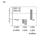
- FIG. 3 is a diagram showing changes in the etching rates of the silicon nitride film and the silicon oxide film depending on whether or not steps S102 to S104 are performed in the etching method according to the first embodiment of the present invention.
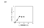
- FIG. 4 is a diagram showing the dependence of the etching rate of the silicon nitride film on the H 2 plasma irradiation time in step S102 in the etching method according to the first embodiment of the present invention.
- FIG. 1 is a cross-sectional view showing a schematic configuration of an etching apparatus according to a first embodiment of the present invention.
- FIG. 2 is a schematic diagram showing an example of the processing procedure of the etching method according to the first embodiment of the present invention.
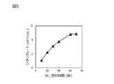
- FIG. 5 is a diagram showing the dependence of the etching rate of the silicon nitride film on the SF 6 plasma irradiation time in step S103 in the etching method according to the first embodiment of the present invention.
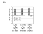
- FIG. 6 is a diagram showing gas species dependence in step S102 of the etching rates of the silicon nitride film and the silicon oxide film in the etching method according to the first embodiment of the present invention.
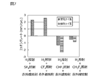
- FIG. 7 is a diagram showing gas species dependence in step S103 of the etching rates of the silicon nitride film and the silicon oxide film in the etching method according to the first embodiment of the present invention.
- FIG. 6 is a diagram showing gas species dependence in step S102 of the etching rates of the silicon nitride film and the silicon oxide film in the etching method according to the first embodiment of the present invention.
- FIG. 7 is a diagram showing gas species dependence in step S103 of the etching rates of the silicon nitride film and the silicon oxide film in
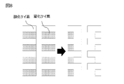
- FIG. 8 is a cross-sectional view of a wafer in each step, showing an example of a processing procedure when processing a multilayer structure including a silicon nitride film using the etching method according to the first embodiment of the present invention.
- FIG. 9 is a schematic diagram showing an example of the processing procedure of the etching method according to the second embodiment of the present invention.
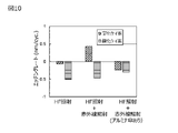
- FIG. 10 is a diagram showing changes in the etching rates of the silicon nitride film and the silicon oxide film depending on whether or not step S107 is performed in the etching method according to the second embodiment of the present invention.
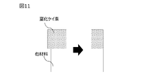
- FIG. 11 is a cross-sectional view of a wafer in each step, showing an example of a processing procedure when processing a multilayer structure including a silicon nitride film using the etching method according to the second embodiment of the present invention.
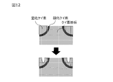
- FIG. 12 is a cross-sectional view of a wafer in each step, showing an example of the processing procedure when a structure including a silicon nitride film is processed using the etching method according to the second embodiment of the present invention.
- the inventors tried etching silicon nitride using various gases. As a result, a modified layer containing hydrogen is formed on the surface by supplying an etchant containing hydrogen to silicon nitride, and a modified layer containing hydrogen and fluorine is formed by supplying an etchant containing fluorine to silicon nitride. It was found that a modified layer is formed on the outermost surface, that the amount of the modified layer produced has self-saturation, and that the modified layer is removed by infrared irradiation.
- a modified layer is formed by supplying an etchant to hydrogen and fluorine on the surface of silicon nitride, and the surface modified layer is removed by infrared irradiation. amount of silicon nitride can be etched.
- a modified layer containing hydrogen and fluorine is formed in advance, and then irradiated with infrared rays to vibrate.
- the vibrational excitation energy of HF corresponds to a wavelength range of about 2.4 ⁇ m, it is possible to cause vibrational excitation by irradiating infrared rays containing the above wavelength range.
- One of the characteristics of the present invention is that a modified layer containing only hydrogen is disposed immediately below a modified layer containing hydrogen and fluorine.
- vibrationally excited HF is generated according to the chemical formula of H 2 +F ⁇ HF * +H (where HF * represents vibrationally excited HF), so it is necessary to supply excess hydrogen with respect to fluorine. .
- the reaction coefficient is larger than the paired reaction of F 2 +H ⁇ HF * +F. Therefore, by arranging a modified layer containing only hydrogen, it becomes possible to generate vibrationally excited HF more efficiently.
- the etching technique of the present invention since processing with self-saturation is performed, the uniformity of the etching amount in the wafer in-plane direction and the pattern depth direction is improved. Furthermore, since the etching amount is determined by the depth of the modified layer and the number of repeated cycle treatments, it is possible to precisely control the etching amount.
- FIG. 1 A first embodiment will be described with reference to FIGS. 1 to 8.
- FIG. 1 silicon nitride is etched using plasma of H2 gas, reactive species generated by plasma of SF6 gas, and infrared irradiation.
- FIG. 1 is a cross-sectional view showing a schematic configuration of an etching apparatus 100 according to this embodiment.
- This etching apparatus 100 includes a wafer stage 102 provided inside a processing chamber 101 , an infrared lamp 103 attached above the wafer stage 102 within the processing chamber 101 , and a plasma lamp provided above the wafer stage 102 .
- a source 104, a gas introduction part 105 attached to the upper part of the plasma source 104, a gas supply part 106 for supplying gas to the gas introduction part 105, a gas exhaust part 107 for exhausting the gas in the processing chamber 101, and FIG. 1 is provided with a control unit (not shown).
- the infrared rays irradiated to the wafer (specimen) on the wafer stage 102 need to oscillate HF to etch silicon nitride as described later. It is necessary to have a light source arrangement and output that can In addition, it is desirable to have a heating mechanism because the heating of the wafer contributes to the removal of etching by-products such as ammonia silicate, ammonia, and silicon fluoride. It is also possible to make the infrared lamp 103 function as a heating mechanism for heating the wafer placed on the wafer stage 102 .
- the gas supply 106 has the ability to selectively supply gases containing hydrogen, gases containing fluorine, and gases containing both hydrogen and fluorine, such as HF.
- gases containing hydrogen include H2, HCl, HF, H2O , NH3 , CH4, and the like.
- gases ( etchants) containing fluorine include SF6 , CF4 , CHF3 , CH2F2 , CH3F , C2F6 , C4F8 , and NF3 .
- the gas supply unit 106 has the ability to supply a reducing gas such as BCl 3 and the ability to supply an inert gas such as argon or nitrogen that allows dilution.
- a gas distribution plate 108 for dispersing the gas introduced from the gas introduction part 105 can be arranged inside the processing chamber 101, and the amount and distribution of ions and radicals generated by the introduced gas and the plasma source 104 can be controlled.
- a shield plate 109 may be arranged between the plasma source 104 and the wafer stage 102 .
- an adjustment mechanism may be provided to adjust the pressure in the processing chamber 101 and adjust the distance between the plasma source 104 and the wafer stage 102 so that ions are not supplied to the wafer.
- the wafer stage 102 preferably has a mechanism for supplying helium gas to the rear surface of the wafer (semiconductor substrate) placed thereon and a cooling mechanism such as a chiller for cooling the wafer stage 102 itself.
- FIG. 2 shows the processing procedure in the silicon nitride film etching method according to this embodiment, and shows the change in the wafer cross-sectional structure in each step of this etching.
- the progress of this processing procedure is controlled by the controller of the etching apparatus 100 .
- step S ⁇ b>101 a wafer with silicon nitride exposed on the surface is placed on the wafer stage 102 .
- step S102 (first step) an etchant containing hydrogen is supplied from the gas supply unit 106 through the gas introduction unit 105 into the processing chamber 101, and the silicon nitride of the wafer is irradiated with the etchant.
- a modified layer (first modified layer) L101 in which hydrogen is bonded is formed.
- step S103 the silicon nitride is irradiated with an etchant containing fluorine through the gas introduction part 105 to form a modified layer (second modified layer) in which hydrogen and fluorine are bonded to the silicon nitride on the outermost surface. ) to form L102.
- step S103 if the etchant contains hydrogen, the fluorine is consumed by the scavenger effect, making it difficult to supply a sufficient amount of fluorine to silicon nitride. Therefore, this etchant does not contain hydrogen. things are desirable.
- radicals are supplied as the etchant in this embodiment, the effect is the same regardless of whether the etchant is supplied in the form of gas or ions. When ions or radicals are used as the etchant, they are generated by the plasma source 104 .
- step S104 infrared rays are irradiated from the infrared lamp 103 to the formed modified layer L101 and modified layer L102. This promotes vibrational excitation of HF to etch the silicon nitride film.
- FIG. 3 compares the results of etching single films of silicon nitride and silicon oxide using radicals generated by H 2 gas plasma, radicals generated by SF 6 gas plasma, and infrared irradiation.
- etching progresses as the positive value of the etching rate increases.
- the etching of the silicon nitride film hardly occurs when there is no H 2 gas plasma irradiation corresponding to step S102 or when there is no infrared irradiation corresponding to step S104.
- significant etching of the silicon nitride film occurs when all steps S102, S103, and S104 are completed. In either case, etching of the silicon oxide film did not occur. From the above results, it can be seen that steps S102, S103 and S104 are necessary to etch the silicon nitride film.
- FIG. 4 and 5 show the relationship between the irradiation time of H 2 gas plasma and SF 6 gas plasma and the etching rate of the silicon nitride film, respectively.
- the etching rate saturates when the irradiation time is extended, which is a so-called self-saturation property.
- the irradiation time indicating self-saturation is longer for SF 6 gas plasma. This is probably because hydrogen atoms have smaller atomic radii than fluorine atoms and, as a result, reach a deeper portion of the sample.
- a modified layer L102 containing hydrogen and fluorine is formed on the outermost surface of the sample, and a modified layer L101 containing only hydrogen is formed immediately below, It can be seen that the silicon nitride film is etched by irradiating the modified layer structure with infrared rays in step S104.
- FIG. 6 shows the etching rate of the silicon nitride film when the gas species is changed in step S102. Etching of the silicon nitride film occurs even if HF is introduced instead of H 2 as the gas. From the above results, it is understood that the etchant introduced in step S102 should contain at least hydrogen.
- FIG. 7 shows the etching rate of the silicon nitride film when the gas species is changed in step S103. Etching of the silicon nitride film occurs even if CF 4 is introduced instead of SF 6 as the gas. On the other hand, when CHF 3 or CH 2 F 2 is introduced, etching of the silicon nitride film does not occur. From the above results, it is understood that the etchant introduced in step S103 should contain fluorine, but it is not desirable that it also contain hydrogen. In step S103, an etchant containing nitrogen may be supplied to the wafer at the same time as the etchant containing fluorine.
- the etching method according to this embodiment has high selectivity with respect to the silicon oxide film. Therefore, adding a step for removing an initial oxide film such as a native oxide film between steps S101 and S102 and introducing a reducing etchant such as BCl3 are also effective in increasing the etching rate. be.
- silicon nitride films contain nitrogen, which moves more easily than silicon, introducing an etchant containing nitrogen such as N2 or NF3 is expected to have self - composite properties, which is effective in reducing roughness. It is considered to be
- Etching of silicon nitride is expected to be applied to a step of removing dummy word lines.
- Fig. 8 shows a schematic diagram of the device structure. Silicon nitride layers and silicon oxide layers are alternately laminated, and by using gas or radicals as an etchant in the present invention, it is possible to selectively etch only silicon nitride in the lateral direction without etching silicon oxide. becomes. Further, according to the method of the present embodiment, since the modified layer having self-saturation is formed as described above, the etching amount can be made uniform above and below the hole. Also, by changing the etching time and the amount of etchant to control the thickness of the modified layer, etc., it is possible to precisely control the amount of etching.
- FIG. 9 A second embodiment will be described with reference to FIGS. 9 to 12.
- FIG. 9 This embodiment relates to an example of etching silicon nitride using reactive species generated by HF gas plasma and infrared irradiation. This embodiment can also be implemented using the etching apparatus shown in FIG.
- the schematic diagram shown in FIG. 9 represents the processing procedure in the silicon nitride film etching method according to the present embodiment, and shows changes in the wafer cross-sectional structure in each step of the etching.
- the progress of this processing procedure is controlled by the controller of the etching apparatus 100 .
- step S105 a wafer with silicon nitride exposed on the surface is placed on the wafer stage 102.
- the silicon nitride is irradiated with an etchant containing HF from the gas introduction part 105 .
- a hydrogen atom has a smaller atomic radius than a fluorine atom, and as a result, reaches a deeper portion of the sample. modified layer), and a modified layer L103 (second modified layer) containing hydrogen is formed immediately below the modified layer L104.
- radicals are supplied as the etchant in this embodiment, the effect is the same regardless of whether the etchant is supplied in the form of gas or ions.
- ions or radicals are used as the etchant, they are generated by the plasma source 104 .
- step S107 the formed modified layers L103 and L104 are irradiated with infrared rays from the infrared lamp 103 to promote vibrational excitation of HF. This causes etching of the silicon nitride film.
- FIG. 10 shows a comparison of the results of etching single films of silicon nitride and silicon oxide using radicals generated by HF gas plasma and infrared irradiation.
- etching progresses as the positive value of the etching rate increases.
- the single film was about 2 cm square and placed on a silicon substrate of 300 mm.
- etching of the silicon nitride film does not occur when there is no infrared irradiation corresponding to step S107.
- steps S106 and S107 are executed, the silicon nitride film is etched, and in either case, the silicon oxide film is not etched.
- steps S106 and S107 are necessary to etch the silicon nitride film. Also, since the silicon nitride film is etched even if the infrared rays are irradiated at the same time as the plasma irradiation of the HF gas, it is understood that the infrared rays may be irradiated simultaneously with the supply of the etchant in order to etch the silicon nitride.
- the above-mentioned etching method of simultaneously irradiating infrared rays can be applied not only to the cycle etching described so far, but also to continuous etching.
- an umbrella made of alumina that does not transmit infrared rays is placed on the silicon nitride film so that only the sample is not directly irradiated with infrared rays, etching of the silicon nitride film does not occur (see FIG. 10).
- Etching of silicon nitride in the actual device structure. Etching of silicon nitride, especially atomic layer etching, which allows precise control of the etching amount, can also be applied to the trimming process for flattening the side walls of the device.
- FIG. 1 A schematic diagram of the device is shown in FIG.
- the silicon nitride remains in a structure protruding from the dissimilar material in the previous step, by using a gas or radical as an etchant in this embodiment, only the silicon nitride is laterally selectively etched without etching the dissimilar material. It is possible to etch to Also, by using ions in this embodiment, anisotropic etching of silicon nitride is possible.
- FIG. 12 shows a schematic diagram of anisotropic etching of silicon nitride sources and drains in a DRAM.
- the modified layer L103 and the modified layer L104 are formed only on the top of the silicon nitride, not on the sidewalls, so anisotropic etching of the silicon nitride film is possible.
- a modified layer containing hydrogen and a modified layer containing hydrogen and fluorine are formed on a silicon nitride film, and then irradiated with infrared rays to generate a sufficient amount of vibrationally excited HF on the silicon nitride film. It becomes possible to supply to the membrane.
- Etching device 101 Processing chamber 101, 102 Wafer stage (cooling device) 103 Infrared lamp (irradiation device) 104 Plasma source 105 Gas introduction unit 106 Gas supply unit, 107 gas exhaust unit (exhaust device), 108 gas dispersion plate, 109 shield plate (shield plate with holes for shielding ions)
Landscapes
- Physics & Mathematics (AREA)
- Engineering & Computer Science (AREA)
- Plasma & Fusion (AREA)
- Chemical & Material Sciences (AREA)
- Analytical Chemistry (AREA)
- Drying Of Semiconductors (AREA)
- Health & Medical Sciences (AREA)
- Toxicology (AREA)
Abstract
Description
水素を有するエッチャントを、窒化ケイ素が表面に出ている試料に供給することにより、水素が窒化ケイ素に結合した第一の改質層を形成する第一の工程と、
フッ素を有するエッチャントを前記試料に供給することにより、水素とフッ素が窒化ケイ素に結合した第二の改質層を、前記第一の改質層の上に形成する第二の工程と、
前記第一の改質層と前記第二の改質層に赤外線を照射する第三の工程、を有することにより達成される。
フッ化水素を有するエッチャントを、窒化ケイ素が表面に出ている試料に供給することにより、水素が窒化ケイ素に結合した第一の改質層と、水素とフッ素が窒化ケイ素に結合した第二の改質層を形成する第四の工程と、
前記第一の改質層と前記第二の改質層に赤外線を照射する第五の工程、を有することにより達成される。
上記した以外の課題、構成及び効果は、以下の実施形態の説明により明らかにされる。
第1の実施形態について、図1から図8を用いて説明する。本実施形態は、H2ガスのプラズマ、SF6ガスのプラズマで生成した反応種、および赤外線照射を用いて、窒化ケイ素をエッチングするものである。
第2の実施形態について、図9から図12を用いて説明する。本実施形態は、HFガスのプラズマで生成した反応種、および赤外線照射を用いて、窒化ケイ素をエッチングする例に関するものである。本実施形態においても、図1に示すエッチング装置を用いて実施できる。
Claims (12)
- 水素を有するエッチャントを、窒化ケイ素が表面に出ている試料に供給することにより、水素が窒化ケイ素に結合した第一の改質層を形成する第一の工程と、
フッ素を有するエッチャントを前記試料に供給することにより、水素とフッ素が窒化ケイ素に結合した第二の改質層を、前記第一の改質層の上に形成する第二の工程と、
前記第一の改質層と前記第二の改質層に赤外線を照射する第三の工程、を有するエッチング方法。 - フッ化水素を有するエッチャントを、窒化ケイ素が表面に出ている試料に供給することにより、水素が窒化ケイ素に結合した第一の改質層と、水素とフッ素が窒化ケイ素に結合した第二の改質層を形成し、
前記第一の改質層と前記第二の改質層に赤外線を照射するエッチング方法。 - 請求項2に記載のエッチング方法において、
前記フッ化水素を有するエッチャントの供給と同時に、前記試料に赤外線を照射するエッチング方法。 - 請求項1に記載のエッチング方法において、
前記第二の工程において、窒素を有するエッチャントを、前記フッ素を有するエッチャントと同時に前記試料に供給するエッチング方法。 - 請求項1に記載のエッチング方法において、
前記第三の工程において、前記第一の改質層と前記第二の改質層を、前記赤外線の照射と同時に加熱するエッチング方法。 - 請求項1に記載のエッチング方法において、
前記第一の工程の前に、前記試料上の初期酸化膜を除去する工程、を有するエッチング方法。 - 請求項1に記載のエッチング方法を実施するエッチング装置であって、
前記試料を内部に収容する処理室と、
前記処理室内に、水素を含むガスとフッ素を含むガスを個別に供給するガス供給部と、
前記処理室内の排気を行う排気装置と、
前記試料に赤外線を照射する照射装置と、
前記試料を冷却する冷却装置と、を有するエッチング装置。 - 請求項7に記載のエッチング装置において、
前記ガス供給部は、前記処理室内にフッ化水素を供給するエッチング装置。 - 請求項7に記載のエッチング装置において、
前記処理室内に、前記ガスからイオンまたはラジカルを生じさせるプラズマ源を有するエッチング装置。 - 請求項9に記載のエッチング装置において、
前記イオンを遮蔽するための穴の開いた遮蔽板を、前記プラズマ源と前記試料との間に配設したエッチング装置。 - 請求項9に記載のエッチング装置において、
前記処理室内の圧力、もしくは前記プラズマ源と前記試料との距離を調整可能な調整機構を有するエッチング処理装置。 - 請求項2に記載のエッチング方法を実施するエッチング装置であって、
前記試料を内部に収容する処理室と、
前記処理室内に、フッ化水素を含むガスを供給するガス供給部と、
前記処理室内の排気を行う排気装置と、
前記試料に赤外線を照射する照射装置と、
前記試料を冷却する冷却装置と、を有するエッチング装置。
Priority Applications (6)
| Application Number | Priority Date | Filing Date | Title |
|---|---|---|---|
| CN202180005347.3A CN115298803A (zh) | 2021-02-19 | 2021-02-19 | 蚀刻方法以及蚀刻装置 |
| KR1020227007192A KR102778730B1 (ko) | 2021-02-19 | 2021-02-19 | 에칭 방법 및 에칭 장치 |
| JP2022509027A JP7372445B2 (ja) | 2021-02-19 | 2021-02-19 | エッチング方法およびエッチング装置 |
| US17/912,943 US20230386793A1 (en) | 2021-02-19 | 2021-02-19 | Etching method and etching apparatus |
| PCT/JP2021/006253 WO2022176142A1 (ja) | 2021-02-19 | 2021-02-19 | エッチング方法およびエッチング装置 |
| TW111105731A TWI826930B (zh) | 2021-02-19 | 2022-02-17 | 蝕刻方法及蝕刻裝置 |
Applications Claiming Priority (1)
| Application Number | Priority Date | Filing Date | Title |
|---|---|---|---|
| PCT/JP2021/006253 WO2022176142A1 (ja) | 2021-02-19 | 2021-02-19 | エッチング方法およびエッチング装置 |
Publications (1)
| Publication Number | Publication Date |
|---|---|
| WO2022176142A1 true WO2022176142A1 (ja) | 2022-08-25 |
Family
ID=82930432
Family Applications (1)
| Application Number | Title | Priority Date | Filing Date |
|---|---|---|---|
| PCT/JP2021/006253 Ceased WO2022176142A1 (ja) | 2021-02-19 | 2021-02-19 | エッチング方法およびエッチング装置 |
Country Status (6)
| Country | Link |
|---|---|
| US (1) | US20230386793A1 (ja) |
| JP (1) | JP7372445B2 (ja) |
| KR (1) | KR102778730B1 (ja) |
| CN (1) | CN115298803A (ja) |
| TW (1) | TWI826930B (ja) |
| WO (1) | WO2022176142A1 (ja) |
Cited By (1)
| Publication number | Priority date | Publication date | Assignee | Title |
|---|---|---|---|---|
| JP2025166525A (ja) * | 2024-04-24 | 2025-11-06 | 株式会社アルバック | エッチング方法、および、エッチング装置 |
Citations (10)
| Publication number | Priority date | Publication date | Assignee | Title |
|---|---|---|---|---|
| JP2008187105A (ja) * | 2007-01-31 | 2008-08-14 | Tokyo Electron Ltd | 基板の処理方法及び基板処理装置 |
| JP2010182730A (ja) * | 2009-02-03 | 2010-08-19 | Tokyo Electron Ltd | 窒化珪素膜のドライエッチング方法 |
| JP2014197603A (ja) * | 2013-03-29 | 2014-10-16 | 東京エレクトロン株式会社 | エッチング方法 |
| JP2015185594A (ja) * | 2014-03-20 | 2015-10-22 | 株式会社日立ハイテクノロジーズ | エッチング装置 |
| JP2018098480A (ja) * | 2016-12-13 | 2018-06-21 | 東京エレクトロン株式会社 | 窒化シリコンから形成された第1領域を酸化シリコンから形成された第2領域に対して選択的にエッチングする方法 |
| JP2018207088A (ja) * | 2017-05-30 | 2018-12-27 | 東京エレクトロン株式会社 | エッチング方法 |
| JP2019012759A (ja) * | 2017-06-30 | 2019-01-24 | 東京エレクトロン株式会社 | エッチング方法およびエッチング装置 |
| JP2019091890A (ja) * | 2017-11-14 | 2019-06-13 | セントラル硝子株式会社 | ドライエッチング方法 |
| JP2020043180A (ja) * | 2018-09-07 | 2020-03-19 | 東京エレクトロン株式会社 | 基板処理装置及び基板処理方法 |
| JP2020088003A (ja) * | 2018-11-16 | 2020-06-04 | 株式会社Screenホールディングス | 基板処理方法、3次元メモリデバイスの製造方法および基板処理装置 |
Family Cites Families (16)
| Publication number | Priority date | Publication date | Assignee | Title |
|---|---|---|---|---|
| JP2840419B2 (ja) * | 1990-09-29 | 1998-12-24 | キヤノン株式会社 | 光処理法及び光処理装置 |
| US6423585B1 (en) * | 1997-03-11 | 2002-07-23 | Semiconductor Energy Laboratory Co., Ltd. | Heating treatment device, heating treatment method and fabrication method of semiconductor device |
| EP1083592A1 (en) * | 1999-09-10 | 2001-03-14 | Interuniversitair Microelektronica Centrum Vzw | Etching of silicon nitride by anhydrous halogen gas |
| WO2001068271A1 (en) * | 2000-03-15 | 2001-09-20 | Tufts University | Controlling surface chemistry on solid substrates |
| US20060062914A1 (en) * | 2004-09-21 | 2006-03-23 | Diwakar Garg | Apparatus and process for surface treatment of substrate using an activated reactive gas |
| JP2011071295A (ja) | 2009-09-25 | 2011-04-07 | Toppan Printing Co Ltd | プラズマエッチング方法及び装置 |
| US9209034B2 (en) * | 2012-02-01 | 2015-12-08 | Tokyo Electron Limited | Plasma etching method and plasma etching apparatus |
| US8716146B2 (en) * | 2012-07-03 | 2014-05-06 | Intermolecular, Inc | Low temperature etching of silicon nitride structures using phosphoric acid solutions |
| RU2620051C2 (ru) * | 2015-10-01 | 2017-05-22 | Федеральное государственное бюджетное образовательное учреждение высшего профессионального образования "Воронежский государственный университет" (ФГБОУ ВПО "ВГУ") | Способ лазерного разделения изотопов фтора |
| JP6817752B2 (ja) | 2016-09-09 | 2021-01-20 | 株式会社日立ハイテク | エッチング方法およびエッチング装置 |
| JP6772117B2 (ja) * | 2017-08-23 | 2020-10-21 | 株式会社日立ハイテク | エッチング方法およびエッチング装置 |
| US10818507B2 (en) * | 2018-05-11 | 2020-10-27 | Tokyo Electron Limited | Method of etching silicon nitride layers for the manufacture of microelectronic workpieces |
| JP2020115498A (ja) * | 2019-01-17 | 2020-07-30 | 東京エレクトロン株式会社 | エッチング方法およびエッチング装置 |
| KR102342124B1 (ko) * | 2019-02-14 | 2021-12-22 | 주식회사 히타치하이테크 | 반도체 제조 장치 |
| KR102904251B1 (ko) * | 2019-02-18 | 2025-12-24 | 도쿄엘렉트론가부시키가이샤 | 에칭 방법 |
| CN115346892A (zh) * | 2021-05-14 | 2022-11-15 | 日扬科技股份有限公司 | 固体结构的加工装置及加工方法 |
-
2021
- 2021-02-19 WO PCT/JP2021/006253 patent/WO2022176142A1/ja not_active Ceased
- 2021-02-19 JP JP2022509027A patent/JP7372445B2/ja active Active
- 2021-02-19 US US17/912,943 patent/US20230386793A1/en active Pending
- 2021-02-19 KR KR1020227007192A patent/KR102778730B1/ko active Active
- 2021-02-19 CN CN202180005347.3A patent/CN115298803A/zh active Pending
-
2022
- 2022-02-17 TW TW111105731A patent/TWI826930B/zh active
Patent Citations (10)
| Publication number | Priority date | Publication date | Assignee | Title |
|---|---|---|---|---|
| JP2008187105A (ja) * | 2007-01-31 | 2008-08-14 | Tokyo Electron Ltd | 基板の処理方法及び基板処理装置 |
| JP2010182730A (ja) * | 2009-02-03 | 2010-08-19 | Tokyo Electron Ltd | 窒化珪素膜のドライエッチング方法 |
| JP2014197603A (ja) * | 2013-03-29 | 2014-10-16 | 東京エレクトロン株式会社 | エッチング方法 |
| JP2015185594A (ja) * | 2014-03-20 | 2015-10-22 | 株式会社日立ハイテクノロジーズ | エッチング装置 |
| JP2018098480A (ja) * | 2016-12-13 | 2018-06-21 | 東京エレクトロン株式会社 | 窒化シリコンから形成された第1領域を酸化シリコンから形成された第2領域に対して選択的にエッチングする方法 |
| JP2018207088A (ja) * | 2017-05-30 | 2018-12-27 | 東京エレクトロン株式会社 | エッチング方法 |
| JP2019012759A (ja) * | 2017-06-30 | 2019-01-24 | 東京エレクトロン株式会社 | エッチング方法およびエッチング装置 |
| JP2019091890A (ja) * | 2017-11-14 | 2019-06-13 | セントラル硝子株式会社 | ドライエッチング方法 |
| JP2020043180A (ja) * | 2018-09-07 | 2020-03-19 | 東京エレクトロン株式会社 | 基板処理装置及び基板処理方法 |
| JP2020088003A (ja) * | 2018-11-16 | 2020-06-04 | 株式会社Screenホールディングス | 基板処理方法、3次元メモリデバイスの製造方法および基板処理装置 |
Non-Patent Citations (1)
| Title |
|---|
| SHERPA SONAM D, RANJAN ALOK: "Quasi-atomic layer etching of silicon nitride ", JOURNAL OF VACUUM SCIENCE & TECHNOLOGY A. VACCUM, SURFACES, AND FILMS, vol. 35, no. 1, 1 January 2017 (2017-01-01), XP055964471 * |
Cited By (2)
| Publication number | Priority date | Publication date | Assignee | Title |
|---|---|---|---|---|
| JP2025166525A (ja) * | 2024-04-24 | 2025-11-06 | 株式会社アルバック | エッチング方法、および、エッチング装置 |
| JP7836848B2 (ja) | 2024-04-24 | 2026-03-27 | 株式会社アルバック | エッチング方法、および、エッチング装置 |
Also Published As
| Publication number | Publication date |
|---|---|
| US20230386793A1 (en) | 2023-11-30 |
| JP7372445B2 (ja) | 2023-10-31 |
| TWI826930B (zh) | 2023-12-21 |
| TW202234513A (zh) | 2022-09-01 |
| KR102778730B1 (ko) | 2025-03-12 |
| CN115298803A (zh) | 2022-11-04 |
| KR20220119358A (ko) | 2022-08-29 |
| JPWO2022176142A1 (ja) | 2022-08-25 |
Similar Documents
| Publication | Publication Date | Title |
|---|---|---|
| JP6817752B2 (ja) | エッチング方法およびエッチング装置 | |
| TWI514462B (zh) | 氮化矽膜中之特徵部的蝕刻方法 | |
| TWI661484B (zh) | 蝕刻方法及蝕刻裝置 | |
| JP6963097B2 (ja) | プラズマ処理方法 | |
| TW201611113A (zh) | 電漿處理方法 | |
| CN104956476A (zh) | 用于垂直nand器件的新型掩模去除方法策略 | |
| JP6619703B2 (ja) | エッチング方法 | |
| CN110660663A (zh) | 蚀刻处理方法以及蚀刻处理装置 | |
| KR102100011B1 (ko) | 에칭 방법 | |
| TWI871572B (zh) | 蝕刻方法 | |
| CN101604630B (zh) | 等离子蚀刻处理方法以及等离子蚀刻处理装置 | |
| TWI907840B (zh) | 蝕刻方法 | |
| JP7372445B2 (ja) | エッチング方法およびエッチング装置 | |
| US20180166290A1 (en) | Method of manufacturing a semiconductor device | |
| JP6579786B2 (ja) | プラズマエッチング方法 | |
| JP7508511B2 (ja) | エッチング処理方法およびエッチング処理装置 | |
| JP7753480B2 (ja) | エッチング処理方法およびエッチング処理装置 | |
| WO2022224412A1 (ja) | エッチング方法 | |
| JP7797677B2 (ja) | ウエハ処理方法およびウエハ処理システム | |
| WO2025182060A1 (ja) | エッチング方法 | |
| WO2026062821A1 (ja) | エッチング方法および半導体装置の製造方法 |
Legal Events
| Date | Code | Title | Description |
|---|---|---|---|
| ENP | Entry into the national phase |
Ref document number: 2022509027 Country of ref document: JP Kind code of ref document: A |
|
| WWE | Wipo information: entry into national phase |
Ref document number: 17912943 Country of ref document: US |
|
| 121 | Ep: the epo has been informed by wipo that ep was designated in this application |
Ref document number: 21926575 Country of ref document: EP Kind code of ref document: A1 |
|
| NENP | Non-entry into the national phase |
Ref country code: DE |
|
| 122 | Ep: pct application non-entry in european phase |
Ref document number: 21926575 Country of ref document: EP Kind code of ref document: A1 |