WO2022163237A1 - 半導体レーザ素子 - Google Patents
半導体レーザ素子 Download PDFInfo
- Publication number
- WO2022163237A1 WO2022163237A1 PCT/JP2021/047705 JP2021047705W WO2022163237A1 WO 2022163237 A1 WO2022163237 A1 WO 2022163237A1 JP 2021047705 W JP2021047705 W JP 2021047705W WO 2022163237 A1 WO2022163237 A1 WO 2022163237A1
- Authority
- WO
- WIPO (PCT)
- Prior art keywords
- layer
- semiconductor
- laser device
- semiconductor laser
- type
- Prior art date
Links
- 239000004065 semiconductor Substances 0.000 title claims abstract description 403
- 239000000758 substrate Substances 0.000 claims abstract description 38
- 238000002347 injection Methods 0.000 claims abstract description 22
- 239000007924 injection Substances 0.000 claims abstract description 22
- 229910052760 oxygen Inorganic materials 0.000 claims description 8
- QVGXLLKOCUKJST-UHFFFAOYSA-N atomic oxygen Chemical compound [O] QVGXLLKOCUKJST-UHFFFAOYSA-N 0.000 claims description 6
- 239000001301 oxygen Substances 0.000 claims description 6
- 230000004048 modification Effects 0.000 description 89
- 238000012986 modification Methods 0.000 description 89
- 239000000203 mixture Substances 0.000 description 69
- 238000005253 cladding Methods 0.000 description 54
- 230000004888 barrier function Effects 0.000 description 53
- 239000012535 impurity Substances 0.000 description 34
- 238000013459 approach Methods 0.000 description 27
- 238000000034 method Methods 0.000 description 16
- 239000011248 coating agent Substances 0.000 description 15
- 238000000576 coating method Methods 0.000 description 15
- 238000004519 manufacturing process Methods 0.000 description 15
- 230000000694 effects Effects 0.000 description 13
- 238000005530 etching Methods 0.000 description 12
- 238000009792 diffusion process Methods 0.000 description 11
- 238000000926 separation method Methods 0.000 description 11
- 238000004088 simulation Methods 0.000 description 11
- 229910001218 Gallium arsenide Inorganic materials 0.000 description 10
- 229910000980 Aluminium gallium arsenide Inorganic materials 0.000 description 8
- 239000007789 gas Substances 0.000 description 8
- 229910004298 SiO 2 Inorganic materials 0.000 description 6
- XUIMIQQOPSSXEZ-UHFFFAOYSA-N Silicon Chemical compound [Si] XUIMIQQOPSSXEZ-UHFFFAOYSA-N 0.000 description 6
- QAOWNCQODCNURD-UHFFFAOYSA-N Sulfuric acid Chemical compound OS(O)(=O)=O QAOWNCQODCNURD-UHFFFAOYSA-N 0.000 description 6
- 239000000463 material Substances 0.000 description 6
- 230000003287 optical effect Effects 0.000 description 6
- 229910052710 silicon Inorganic materials 0.000 description 6
- 239000010703 silicon Substances 0.000 description 6
- OKTJSMMVPCPJKN-UHFFFAOYSA-N Carbon Chemical compound [C] OKTJSMMVPCPJKN-UHFFFAOYSA-N 0.000 description 5
- 229910052799 carbon Inorganic materials 0.000 description 5
- 230000008859 change Effects 0.000 description 5
- 238000005424 photoluminescence Methods 0.000 description 5
- KRHYYFGTRYWZRS-UHFFFAOYSA-N Fluorane Chemical compound F KRHYYFGTRYWZRS-UHFFFAOYSA-N 0.000 description 4
- 230000031700 light absorption Effects 0.000 description 4
- 239000007788 liquid Substances 0.000 description 4
- 238000000206 photolithography Methods 0.000 description 4
- 238000001039 wet etching Methods 0.000 description 4
- MHAJPDPJQMAIIY-UHFFFAOYSA-N Hydrogen peroxide Chemical compound OO MHAJPDPJQMAIIY-UHFFFAOYSA-N 0.000 description 3
- 239000000969 carrier Substances 0.000 description 3
- 239000000470 constituent Substances 0.000 description 3
- 230000007423 decrease Effects 0.000 description 3
- 238000009413 insulation Methods 0.000 description 3
- 230000010355 oscillation Effects 0.000 description 3
- 229910018072 Al 2 O 3 Inorganic materials 0.000 description 2
- QGZKDVFQNNGYKY-UHFFFAOYSA-N Ammonia Chemical compound N QGZKDVFQNNGYKY-UHFFFAOYSA-N 0.000 description 2
- VYPSYNLAJGMNEJ-UHFFFAOYSA-N Silicium dioxide Chemical compound O=[Si]=O VYPSYNLAJGMNEJ-UHFFFAOYSA-N 0.000 description 2
- 230000003321 amplification Effects 0.000 description 2
- 229910052804 chromium Inorganic materials 0.000 description 2
- 239000012141 concentrate Substances 0.000 description 2
- 239000013078 crystal Substances 0.000 description 2
- 238000005520 cutting process Methods 0.000 description 2
- 230000006866 deterioration Effects 0.000 description 2
- 229910052737 gold Inorganic materials 0.000 description 2
- 230000017525 heat dissipation Effects 0.000 description 2
- 238000003475 lamination Methods 0.000 description 2
- 239000002184 metal Substances 0.000 description 2
- 229910052751 metal Inorganic materials 0.000 description 2
- 229910052750 molybdenum Inorganic materials 0.000 description 2
- 229910052759 nickel Inorganic materials 0.000 description 2
- 238000003199 nucleic acid amplification method Methods 0.000 description 2
- 230000003647 oxidation Effects 0.000 description 2
- 238000007254 oxidation reaction Methods 0.000 description 2
- 238000001020 plasma etching Methods 0.000 description 2
- 238000007747 plating Methods 0.000 description 2
- 229910052697 platinum Inorganic materials 0.000 description 2
- 230000001681 protective effect Effects 0.000 description 2
- 239000000243 solution Substances 0.000 description 2
- 229910052719 titanium Inorganic materials 0.000 description 2
- XLYOFNOQVPJJNP-UHFFFAOYSA-N water Substances O XLYOFNOQVPJJNP-UHFFFAOYSA-N 0.000 description 2
- ZCYVEMRRCGMTRW-UHFFFAOYSA-N 7553-56-2 Chemical compound [I] ZCYVEMRRCGMTRW-UHFFFAOYSA-N 0.000 description 1
- FEWJPZIEWOKRBE-JCYAYHJZSA-N Dextrotartaric acid Chemical compound OC(=O)[C@H](O)[C@@H](O)C(O)=O FEWJPZIEWOKRBE-JCYAYHJZSA-N 0.000 description 1
- FEWJPZIEWOKRBE-UHFFFAOYSA-N Tartaric acid Natural products [H+].[H+].[O-]C(=O)C(O)C(O)C([O-])=O FEWJPZIEWOKRBE-UHFFFAOYSA-N 0.000 description 1
- 238000010521 absorption reaction Methods 0.000 description 1
- 229910021529 ammonia Inorganic materials 0.000 description 1
- 230000015572 biosynthetic process Effects 0.000 description 1
- 230000000903 blocking effect Effects 0.000 description 1
- 238000003776 cleavage reaction Methods 0.000 description 1
- 229910052681 coesite Inorganic materials 0.000 description 1
- 150000001875 compounds Chemical class 0.000 description 1
- 229910052906 cristobalite Inorganic materials 0.000 description 1
- 238000010586 diagram Methods 0.000 description 1
- 238000009826 distribution Methods 0.000 description 1
- 238000001312 dry etching Methods 0.000 description 1
- 238000005566 electron beam evaporation Methods 0.000 description 1
- 238000010894 electron beam technology Methods 0.000 description 1
- 238000009713 electroplating Methods 0.000 description 1
- 239000011810 insulating material Substances 0.000 description 1
- 239000012212 insulator Substances 0.000 description 1
- 229910052740 iodine Inorganic materials 0.000 description 1
- 239000011630 iodine Substances 0.000 description 1
- 238000002955 isolation Methods 0.000 description 1
- 239000011259 mixed solution Substances 0.000 description 1
- 150000007524 organic acids Chemical class 0.000 description 1
- 230000001590 oxidative effect Effects 0.000 description 1
- 150000002978 peroxides Chemical class 0.000 description 1
- 238000009832 plasma treatment Methods 0.000 description 1
- 238000000623 plasma-assisted chemical vapour deposition Methods 0.000 description 1
- 230000010287 polarization Effects 0.000 description 1
- 230000001737 promoting effect Effects 0.000 description 1
- 230000001902 propagating effect Effects 0.000 description 1
- 230000006798 recombination Effects 0.000 description 1
- 238000005215 recombination Methods 0.000 description 1
- 229910052594 sapphire Inorganic materials 0.000 description 1
- 239000010980 sapphire Substances 0.000 description 1
- 230000007017 scission Effects 0.000 description 1
- 239000000377 silicon dioxide Substances 0.000 description 1
- 235000012239 silicon dioxide Nutrition 0.000 description 1
- 229910000679 solder Inorganic materials 0.000 description 1
- 229910052682 stishovite Inorganic materials 0.000 description 1
- 239000000126 substance Substances 0.000 description 1
- 235000002906 tartaric acid Nutrition 0.000 description 1
- 239000011975 tartaric acid Substances 0.000 description 1
- 229910052905 tridymite Inorganic materials 0.000 description 1
- 238000007740 vapor deposition Methods 0.000 description 1
Images


Classifications
-
- H—ELECTRICITY
- H01—ELECTRIC ELEMENTS
- H01S—DEVICES USING THE PROCESS OF LIGHT AMPLIFICATION BY STIMULATED EMISSION OF RADIATION [LASER] TO AMPLIFY OR GENERATE LIGHT; DEVICES USING STIMULATED EMISSION OF ELECTROMAGNETIC RADIATION IN WAVE RANGES OTHER THAN OPTICAL
- H01S5/00—Semiconductor lasers
- H01S5/20—Structure or shape of the semiconductor body to guide the optical wave ; Confining structures perpendicular to the optical axis, e.g. index or gain guiding, stripe geometry, broad area lasers, gain tailoring, transverse or lateral reflectors, special cladding structures, MQW barrier reflection layers
- H01S5/22—Structure or shape of the semiconductor body to guide the optical wave ; Confining structures perpendicular to the optical axis, e.g. index or gain guiding, stripe geometry, broad area lasers, gain tailoring, transverse or lateral reflectors, special cladding structures, MQW barrier reflection layers having a ridge or stripe structure
-
- H—ELECTRICITY
- H01—ELECTRIC ELEMENTS
- H01S—DEVICES USING THE PROCESS OF LIGHT AMPLIFICATION BY STIMULATED EMISSION OF RADIATION [LASER] TO AMPLIFY OR GENERATE LIGHT; DEVICES USING STIMULATED EMISSION OF ELECTROMAGNETIC RADIATION IN WAVE RANGES OTHER THAN OPTICAL
- H01S5/00—Semiconductor lasers
- H01S5/02—Structural details or components not essential to laser action
- H01S5/028—Coatings ; Treatment of the laser facets, e.g. etching, passivation layers or reflecting layers
- H01S5/0287—Facet reflectivity
-
- H—ELECTRICITY
- H01—ELECTRIC ELEMENTS
- H01S—DEVICES USING THE PROCESS OF LIGHT AMPLIFICATION BY STIMULATED EMISSION OF RADIATION [LASER] TO AMPLIFY OR GENERATE LIGHT; DEVICES USING STIMULATED EMISSION OF ELECTROMAGNETIC RADIATION IN WAVE RANGES OTHER THAN OPTICAL
- H01S5/00—Semiconductor lasers
- H01S5/04—Processes or apparatus for excitation, e.g. pumping, e.g. by electron beams
- H01S5/042—Electrical excitation ; Circuits therefor
- H01S5/0421—Electrical excitation ; Circuits therefor characterised by the semiconducting contacting layers
-
- H—ELECTRICITY
- H01—ELECTRIC ELEMENTS
- H01S—DEVICES USING THE PROCESS OF LIGHT AMPLIFICATION BY STIMULATED EMISSION OF RADIATION [LASER] TO AMPLIFY OR GENERATE LIGHT; DEVICES USING STIMULATED EMISSION OF ELECTROMAGNETIC RADIATION IN WAVE RANGES OTHER THAN OPTICAL
- H01S5/00—Semiconductor lasers
- H01S5/04—Processes or apparatus for excitation, e.g. pumping, e.g. by electron beams
- H01S5/042—Electrical excitation ; Circuits therefor
- H01S5/0425—Electrodes, e.g. characterised by the structure
- H01S5/04252—Electrodes, e.g. characterised by the structure characterised by the material
-
- H—ELECTRICITY
- H01—ELECTRIC ELEMENTS
- H01S—DEVICES USING THE PROCESS OF LIGHT AMPLIFICATION BY STIMULATED EMISSION OF RADIATION [LASER] TO AMPLIFY OR GENERATE LIGHT; DEVICES USING STIMULATED EMISSION OF ELECTROMAGNETIC RADIATION IN WAVE RANGES OTHER THAN OPTICAL
- H01S5/00—Semiconductor lasers
- H01S5/04—Processes or apparatus for excitation, e.g. pumping, e.g. by electron beams
- H01S5/042—Electrical excitation ; Circuits therefor
- H01S5/0425—Electrodes, e.g. characterised by the structure
- H01S5/04254—Electrodes, e.g. characterised by the structure characterised by the shape
-
- H—ELECTRICITY
- H01—ELECTRIC ELEMENTS
- H01S—DEVICES USING THE PROCESS OF LIGHT AMPLIFICATION BY STIMULATED EMISSION OF RADIATION [LASER] TO AMPLIFY OR GENERATE LIGHT; DEVICES USING STIMULATED EMISSION OF ELECTROMAGNETIC RADIATION IN WAVE RANGES OTHER THAN OPTICAL
- H01S5/00—Semiconductor lasers
- H01S5/10—Construction or shape of the optical resonator, e.g. extended or external cavity, coupled cavities, bent-guide, varying width, thickness or composition of the active region
- H01S5/16—Window-type lasers, i.e. with a region of non-absorbing material between the active region and the reflecting surface
- H01S5/162—Window-type lasers, i.e. with a region of non-absorbing material between the active region and the reflecting surface with window regions made by diffusion or disordening of the active layer
-
- H—ELECTRICITY
- H01—ELECTRIC ELEMENTS
- H01S—DEVICES USING THE PROCESS OF LIGHT AMPLIFICATION BY STIMULATED EMISSION OF RADIATION [LASER] TO AMPLIFY OR GENERATE LIGHT; DEVICES USING STIMULATED EMISSION OF ELECTROMAGNETIC RADIATION IN WAVE RANGES OTHER THAN OPTICAL
- H01S5/00—Semiconductor lasers
- H01S5/30—Structure or shape of the active region; Materials used for the active region
- H01S5/305—Structure or shape of the active region; Materials used for the active region characterised by the doping materials used in the laser structure
-
- H—ELECTRICITY
- H01—ELECTRIC ELEMENTS
- H01S—DEVICES USING THE PROCESS OF LIGHT AMPLIFICATION BY STIMULATED EMISSION OF RADIATION [LASER] TO AMPLIFY OR GENERATE LIGHT; DEVICES USING STIMULATED EMISSION OF ELECTROMAGNETIC RADIATION IN WAVE RANGES OTHER THAN OPTICAL
- H01S2301/00—Functional characteristics
- H01S2301/17—Semiconductor lasers comprising special layers
- H01S2301/176—Specific passivation layers on surfaces other than the emission facet
-
- H—ELECTRICITY
- H01—ELECTRIC ELEMENTS
- H01S—DEVICES USING THE PROCESS OF LIGHT AMPLIFICATION BY STIMULATED EMISSION OF RADIATION [LASER] TO AMPLIFY OR GENERATE LIGHT; DEVICES USING STIMULATED EMISSION OF ELECTROMAGNETIC RADIATION IN WAVE RANGES OTHER THAN OPTICAL
- H01S2301/00—Functional characteristics
- H01S2301/18—Semiconductor lasers with special structural design for influencing the near- or far-field
-
- H—ELECTRICITY
- H01—ELECTRIC ELEMENTS
- H01S—DEVICES USING THE PROCESS OF LIGHT AMPLIFICATION BY STIMULATED EMISSION OF RADIATION [LASER] TO AMPLIFY OR GENERATE LIGHT; DEVICES USING STIMULATED EMISSION OF ELECTROMAGNETIC RADIATION IN WAVE RANGES OTHER THAN OPTICAL
- H01S5/00—Semiconductor lasers
- H01S5/0014—Measuring characteristics or properties thereof
-
- H—ELECTRICITY
- H01—ELECTRIC ELEMENTS
- H01S—DEVICES USING THE PROCESS OF LIGHT AMPLIFICATION BY STIMULATED EMISSION OF RADIATION [LASER] TO AMPLIFY OR GENERATE LIGHT; DEVICES USING STIMULATED EMISSION OF ELECTROMAGNETIC RADIATION IN WAVE RANGES OTHER THAN OPTICAL
- H01S5/00—Semiconductor lasers
- H01S5/10—Construction or shape of the optical resonator, e.g. extended or external cavity, coupled cavities, bent-guide, varying width, thickness or composition of the active region
- H01S5/16—Window-type lasers, i.e. with a region of non-absorbing material between the active region and the reflecting surface
- H01S5/168—Window-type lasers, i.e. with a region of non-absorbing material between the active region and the reflecting surface with window regions comprising current blocking layers
-
- H—ELECTRICITY
- H01—ELECTRIC ELEMENTS
- H01S—DEVICES USING THE PROCESS OF LIGHT AMPLIFICATION BY STIMULATED EMISSION OF RADIATION [LASER] TO AMPLIFY OR GENERATE LIGHT; DEVICES USING STIMULATED EMISSION OF ELECTROMAGNETIC RADIATION IN WAVE RANGES OTHER THAN OPTICAL
- H01S5/00—Semiconductor lasers
- H01S5/30—Structure or shape of the active region; Materials used for the active region
- H01S5/32—Structure or shape of the active region; Materials used for the active region comprising PN junctions, e.g. hetero- or double- heterostructures
- H01S5/3201—Structure or shape of the active region; Materials used for the active region comprising PN junctions, e.g. hetero- or double- heterostructures incorporating bulkstrain effects, e.g. strain compensation, strain related to polarisation
-
- H—ELECTRICITY
- H01—ELECTRIC ELEMENTS
- H01S—DEVICES USING THE PROCESS OF LIGHT AMPLIFICATION BY STIMULATED EMISSION OF RADIATION [LASER] TO AMPLIFY OR GENERATE LIGHT; DEVICES USING STIMULATED EMISSION OF ELECTROMAGNETIC RADIATION IN WAVE RANGES OTHER THAN OPTICAL
- H01S5/00—Semiconductor lasers
- H01S5/30—Structure or shape of the active region; Materials used for the active region
- H01S5/34—Structure or shape of the active region; Materials used for the active region comprising quantum well or superlattice structures, e.g. single quantum well [SQW] lasers, multiple quantum well [MQW] lasers or graded index separate confinement heterostructure [GRINSCH] lasers
- H01S5/343—Structure or shape of the active region; Materials used for the active region comprising quantum well or superlattice structures, e.g. single quantum well [SQW] lasers, multiple quantum well [MQW] lasers or graded index separate confinement heterostructure [GRINSCH] lasers in AIIIBV compounds, e.g. AlGaAs-laser, InP-based laser
- H01S5/34313—Structure or shape of the active region; Materials used for the active region comprising quantum well or superlattice structures, e.g. single quantum well [SQW] lasers, multiple quantum well [MQW] lasers or graded index separate confinement heterostructure [GRINSCH] lasers in AIIIBV compounds, e.g. AlGaAs-laser, InP-based laser with a well layer having only As as V-compound, e.g. AlGaAs, InGaAs
Definitions
- the present disclosure relates to a semiconductor laser device.
- the semiconductor laser device described in Patent Document 1 includes a semiconductor laminate including an N-type clad layer, an active layer, a P-type clad layer, and a P-type contact layer, and an insulator having an opening disposed on the semiconductor laminate. and a P-side electrode disposed on the insulating film. An opening is formed in the insulating film, and current is supplied from the P-side electrode to the semiconductor laminate via the opening. The opening is not formed near the facet forming the cavity of the semiconductor laser element. Accordingly, in the semiconductor laser device described in Patent Document 1, COD (catastrophic optical damage) in the vicinity of the facet is suppressed by suppressing current supply in the vicinity of the facet.
- COD catastrophic optical damage
- the P-type contact layer extends from one facet to the other facet. A current can be supplied through the layers to the vicinity of the end face. Therefore, in the semiconductor laser device described in Patent Document 1, COD may occur near the facet.
- the present disclosure aims to solve such problems, and aims to provide a semiconductor laser device capable of suppressing COD near the facet.
- one aspect of the semiconductor laser device is a semiconductor laser device that emits multi-lateral mode laser light, comprising: a substrate; and a semiconductor laminate disposed above the substrate.
- the semiconductor laminate includes an N-side semiconductor layer arranged above the substrate, an active layer arranged above the N-side semiconductor layer, and a P-side semiconductor layer arranged above the active layer a semiconductor layer and a p-type contact layer disposed above the p-side semiconductor layer; the semiconductor laminate has two facets facing each other;
- the semiconductor laminate includes a ridge portion extending in the resonance direction of the laser light and a part of the upper surface of the semiconductor laminate, wherein the ridge portion is seen in a top view of the semiconductor laminate.
- a current injection window which is a region into which a current is injected, is formed only on the ridge portion of the upper surface of the semiconductor laminate, and the distance from the upper surface of the active layer to the bottom portion is uniform. is.
- one aspect of the semiconductor laser device is a semiconductor laser device that emits multi-lateral mode laser light, comprising: a substrate; a stacked body, wherein the semiconductor stacked body includes an N-side semiconductor layer disposed above the substrate, an active layer disposed above the N-side semiconductor layer, and an active layer disposed above the active layer. It has a P-side semiconductor layer and a P-type contact layer arranged above the P-side semiconductor layer, the semiconductor laminate has two end faces facing each other, and the laser light Resonates between the end faces, and the semiconductor laminate includes a ridge portion extending in the resonance direction of the laser light and a part of the upper surface of the semiconductor laminate.
- a current injection window which is a region into which a current is injected, is formed only on the ridge portion of the upper surface of the semiconductor laminate, and the P-type contact layer is exposed on the bottom portion. is doing.
- FIG. 1 is a schematic plan view showing the overall configuration of a semiconductor laser device according to an embodiment.
- FIG. 2 is a schematic first cross-sectional view showing the overall configuration of the semiconductor laser device according to the embodiment.
- FIG. 3 is a schematic second cross-sectional view showing the overall configuration of the semiconductor laser device according to the embodiment.
- FIG. 4 is a schematic third cross-sectional view showing the overall configuration of the semiconductor laser device according to the embodiment.
- FIG. 5 is a schematic cross-sectional view showing a configuration example of an N-side semiconductor layer according to the embodiment.
- FIG. 6 is a schematic cross-sectional view showing a configuration example of an active layer according to the embodiment.
- FIG. 7 is a schematic cross-sectional view showing a configuration example of the P-side semiconductor layer according to the embodiment.
- FIG. 1 is a schematic plan view showing the overall configuration of a semiconductor laser device according to an embodiment.
- FIG. 2 is a schematic first cross-sectional view showing the overall configuration of the semiconductor laser device according to the
- FIG. 8 is a cross-sectional view showing the structure of the model used in the simulation of the semiconductor laser device according to the embodiment.
- FIG. 9 is a graph showing simulation results of current spread in the lateral direction of the semiconductor laser device according to the embodiment.
- FIG. 10 is a graph in which a part of FIG. 9 is enlarged.
- FIG. 11 is a graph showing simulation results of the lateral width of the near-field pattern (NFP) of the semiconductor laser device according to the embodiment.
- FIG. 12 is a graph showing simulation results of current spread in the resonance direction of the semiconductor laser device according to the embodiment.
- FIG. 13 is a graph showing the relationship between the distance from the top surface to the bottom of the active layer and the effective refractive index difference.
- FIG. 9 is a graph showing simulation results of current spread in the lateral direction of the semiconductor laser device according to the embodiment.
- FIG. 10 is a graph in which a part of FIG. 9 is enlarged.
- FIG. 11 is a graph showing simulation results of the lateral width of
- FIG. 14 is a schematic cross-sectional view showing the first step of the method of manufacturing the semiconductor laser device according to the embodiment.
- FIG. 15 is a schematic cross-sectional view showing the second step of the method for manufacturing the semiconductor laser device according to the embodiment.
- FIG. 16 is a schematic first cross-sectional view showing the third step of the method for manufacturing the semiconductor laser device according to the embodiment.
- FIG. 17 is a schematic second cross-sectional view showing the third step of the method for manufacturing the semiconductor laser device according to the embodiment.
- FIG. 18 is a schematic first cross-sectional view showing the fourth step of the method for manufacturing the semiconductor laser device according to the embodiment.
- FIG. 19 is a schematic second cross-sectional view showing the fourth step of the method for manufacturing the semiconductor laser device according to the embodiment.
- FIG. 20 is a schematic first cross-sectional view showing the fifth step of the method for manufacturing the semiconductor laser device according to the embodiment.
- FIG. 21 is a schematic second cross-sectional view showing the fifth step of the method for manufacturing the semiconductor laser device according to the embodiment.
- FIG. 22 is a schematic first cross-sectional view showing the sixth step of the method of manufacturing the semiconductor laser device according to the embodiment.
- FIG. 23 is a schematic second cross-sectional view showing the sixth step of the method for manufacturing the semiconductor laser device according to the embodiment.
- 24 is a schematic plan view showing the overall configuration of a semiconductor laser device according to Modification 4.
- FIG. 25 is a schematic plan view showing the overall configuration of a semiconductor laser device according to Modification 5.
- FIG. 26 is a schematic plan view showing the overall configuration of a semiconductor laser device according to Modification 6.
- FIG. 27 is a schematic plan view showing the overall configuration of a semiconductor laser device according to Modification 7.
- FIG. 28 is a schematic plan view showing the overall configuration of a semiconductor laser device according to Modification 8.
- FIG. 29 is a schematic cross-sectional view showing the overall configuration of a semiconductor laser device according to Modification 8. As shown in FIG.
- each figure is a schematic diagram and is not necessarily strictly illustrated. Therefore, the scales and the like are not always the same in each drawing.
- symbol is attached
- the terms “upper” and “lower” do not refer to the upward direction (vertically upward) and the downward direction (vertically downward) in absolute spatial recognition, but are based on the stacking order in the stacking structure. It is used as a term defined by a relative positional relationship. Also, the terms “above” and “below” are used not only when two components are spaced apart from each other and there is another component between the two components, but also when two components are spaced apart from each other. It also applies when they are arranged in contact with each other.
- FIG. 1 is a schematic plan view showing the overall configuration of a semiconductor laser device 10 according to this embodiment.
- 2 to 4 are schematic cross-sectional views showing the overall configuration of the semiconductor laser device 10 according to this embodiment. 2, 3, and 4 show cross sections taken along lines II-II, III-III, and IV-IV of FIG. 1, respectively.
- Each figure shows an X-axis, a Y-axis, and a Z-axis that are orthogonal to each other.
- the X, Y, and Z axes are a right-handed Cartesian coordinate system.
- the stacking direction of the semiconductor laser element 10 is parallel to the Z-axis direction, and the main emission direction of light (laser light in this embodiment) is parallel to the Y-axis direction.
- the semiconductor laser device 10 is a device that emits multi-lateral mode laser light.
- the semiconductor laser device 10 includes a substrate 21 and a semiconductor laminate 10S.
- the semiconductor laminate 10S has two end faces 10F and 10R that are perpendicular to the lamination direction (that is, the Z-axis direction) and face each other (see FIG. 1).
- the two facets 10F and 10R form a resonator, and the semiconductor laminate 10S emits laser light from the facet 10F.
- the semiconductor laminate 10S includes an optical waveguide positioned between the two end faces 10F and 10R for guiding laser light.
- the waveguide characteristic of the semiconductor laser device 10 is of gain waveguide type.
- the cavity length of the semiconductor laser device 10 (that is, the distance between the facets 10F and 10R) is 2 mm or more.
- the cavity length of the semiconductor laser device 10 may be 4 mm or more, or may be less than 2 mm.
- the end surface 10F is a front end surface that emits laser light
- the end surface 10R is a rear end surface having a higher reflectance than the end surface 10F.
- a first facet coating film 71 is arranged on the facet 10F, and a second facet coating film 72 is arranged on the facet 10R.
- the first facet coating film 71 and the second facet coating film 72 are films for adjusting the reflectance of laser light on each facet.
- the first facet coat film 71 and the second facet coat film 72 are multilayer films formed of dielectric multilayer films.
- the first facet coating film 71 is a multilayer film including one or more Al 2 O 3 films and one or more Ta 2 O 5 films
- the second facet coating film 72 is one or more Al 2 O 3 film, one or more layers of SiO 2 film, and one or more layers of Ta 2 O 5 film.
- the reflectance of the first facet coating film 71 is 2%, and the reflectance of the second facet coating film 72 is 95%.
- the two end faces of the substrate 21 in the resonance direction are on the same plane as the end faces 10F and 10R of the semiconductor laminate 10S, respectively (see FIG. 4).
- a first facet coating film 71 and a second facet coating film 72 are also arranged on two facets of the substrate 21 in the resonance direction, respectively.
- the reflectances of the first facet coating film 71 and the second facet coating film 72 are not limited to the reflectances described above.
- the reflectance of the first facet coating film 71 may be 0.2% or less.
- the kink is a phenomenon in which the power of the output laser light changes discontinuously with respect to changes in the current supplied to the semiconductor laser device 10 .
- the kink is a phenomenon in which a graph showing the relationship between the current supplied to the semiconductor laser element 10 and the power of the output laser light has discontinuous changes.
- the semiconductor laser device 10 emits laser light with a wavelength of 900 nm or more and 980 nm or less.
- the semiconductor laminate 10S of the semiconductor laser device 10 is composed of, for example, a III-V group compound semiconductor made of AlGaInAs-based material.
- the semiconductor laser element 10 emits laser light with a wavelength of 976 nm, for example.
- the semiconductor laser device 10 has a facet window structure, the details of which will be described later.
- the semiconductor laminate 10S of the semiconductor laser device 10 has a window region 10w adjacent to the laser beam emitting facet 10F (that is, the front facet) of the two facets, as shown in FIG.
- window region 10w contacts end surface 10F.
- the semiconductor laminate 10S may further have a window region 10w adjacent to the end surface 10R.
- semiconductor laminate 10S has window region 10w adjacent to end surface 10R.
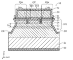
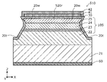
- the semiconductor laser element 10 includes a substrate 21, a semiconductor laminate 10S, an insulating film 30, a first P-side electrode 41, a pad electrode 50, a second P-side electrode 42, and an N-side electrode 60 .
- the substrate 21 is a plate-like member that serves as a base for the semiconductor laser element 10 .
- the substrate 21 is a plate-like member having a principal surface that is uniformly flat.
- the substrate 21 is a semiconductor substrate such as a GaAs substrate or an insulating substrate such as a sapphire substrate. In this embodiment, the substrate 21 is an N-type GaAs substrate.
- the semiconductor laminate 10S is a laminate arranged above the substrate 21 .
- the semiconductor laminate 10S has a plurality of semiconductor layers laminated in the lamination direction (that is, the Z-axis direction in each figure).
- the semiconductor laminate 10S has an N-side semiconductor layer 22, an active layer 23, a P-side semiconductor layer 24, and a P-type contact layer 25.
- the semiconductor laminate 10S has a ridge portion 20r extending in the resonance direction of the laser light, and a bottom portion 20b surrounding the ridge portion 20r in a top view of the semiconductor laminate 10S.
- the bottom portion 20b is part of the upper surface of the semiconductor stacked body 10S.
- the ridge portion 20r protrudes upward from the bottom portion 20b and includes at least a portion of the P-type contact layer 25, as shown in FIG. Also, as shown in FIGS. 1 and 4, the ridge portion 20r is separated from the two end surfaces 10F and 10R.
- the ridge portion 20r of the semiconductor laminate 10S constitutes the optical waveguide of the semiconductor laser element 10. As shown in FIG. In this embodiment, the width of the ridge portion 20r (that is, the dimension in the X-axis direction) is 230 ⁇ m.
- the distance Db in the stacking direction from the upper surface of the active layer 23 to the bottom portion 20b is uniform.
- the bottom portion 20b lies on a plane perpendicular to the stacking direction. This allows the entire bottom portion 20b to be formed simultaneously by etching or the like.
- the configuration in which the distance Db is uniform includes not only a configuration in which the distance Db is the same at any position on the bottom portion 20b, but also a configuration in which the distance Db is substantially the same. For example, a configuration in which the error of the distance Db is 5% or less is also included in the configuration in which the distance Db is uniform. In this embodiment, as shown in FIGS.
- the P-side semiconductor layer 24 is exposed at the bottom portion 20b. That is, the distance Db is equal to or less than the film thickness of the P-side semiconductor layer 24 .
- the structure of the bottom part 20b which concerns on this Embodiment is not limited to this. That is, the distance Db in the stacking direction from the upper surface of the active layer 23 to the bottom portion 20b may not be uniform.
- the bottom portion 20b may have a region inclined with respect to the XY plane, or may have a stepped portion.
- a current injection window 25a which is a region into which current is injected, is formed only on the ridge portion 20r of the upper surface of the semiconductor stacked body 10S.
- the current injection window 25a is a region where the P-type contact layer 25 of the semiconductor laminate 10S and the first P-side electrode 41 are in contact.
- the semiconductor laminate 10S has two wing portions 20w that include part of the P-type contact layer 25 and extend in the resonance direction. At least part of the ridge portion 20r is arranged between the two wing portions 20w in the top view of the semiconductor stacked body 10S. Each of the two wing portions 20w is adjacent to the ridge portion 20r via the bottom portion 20b. As shown in FIGS. 2 and 3, two wing portions 20w protrude upward from the bottom portion 20b. The height of the two wings 20w from the bottom 20b is equal to the height of the ridge 20r from the bottom 20b.
- the stress applied to the semiconductor laser element 10 is dispersed to the wing portions 20w, so that the stress can be prevented from concentrating only on the ridge portion 20r. Therefore, it is possible to prevent the ridge portion 20r from being damaged.
- the configuration in which the height of the two wing portions 20w from the bottom portion 20b is equal to the height of the ridge portion 20r from the bottom portion 20b includes not only a configuration in which each height is completely equal, but also a configuration in which the heights are substantially equal. be For example, a configuration in which each height has an error of 5% or less is also included in the configuration in which each height is equal.
- Each of the two wing portions 20w extends to the two end faces 10F and 10R. In this embodiment, each of the two wing portions 20w extends from the end surface 10F to the end surface 10R.
- the stress applied to the ridge portion 20r can be reduced in the vicinity of the end surfaces 10F and 10R where stress tends to concentrate. Therefore, it is possible to prevent the ridge portion 20r from being damaged.
- the width of the bottom portion 20b between the ridge portion 20r and the wing portion 20w may be 5 ⁇ m or more and 30 ⁇ m or less. Thereby, the shear stress outside the ridge portion 20r can be reduced. If the width of the bottom portion 20b is too large, the load during mounting concentrates on the ridge portion 20r, which serves as a current injection region. good too. As a result, it is possible to effectively suppress the rotation of the plane of polarization due to the shear stress, and reduce the influence of the shear stress on the laser light propagating through the optical waveguide.
- separation grooves 20t are formed at both ends of the semiconductor laminate 10S in the X-axis direction.
- the separation groove 20t is a groove used when singulating the semiconductor stacked body 10S.
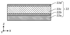
- the N-side semiconductor layer 22 is an example of a first conductivity type first semiconductor layer arranged above the substrate 21 and below the active layer 23 .
- a configuration example of the N-side semiconductor layer 22 according to the present embodiment will be described below with reference to FIG.
- FIG. 5 is a schematic cross-sectional view showing a configuration example of the N-side semiconductor layer 22 according to this embodiment.
- the N-side semiconductor layer 22 includes an N-type buffer layer 22a, a first N-type composition graded layer 22b, an N-type cladding layer 22c, a second N-type composition and a sloped layer 22d.
- the N-type buffer layer 22a, the first N-type composition gradient layer 22b, the N-type cladding layer 22c, and the second N-type composition gradient layer 22d are N-type semiconductor layers intentionally doped with impurities. Examples include an N-type GaAs layer and an N-type AlGaAs layer. Silicon (Si), for example, can be used as an impurity to be doped into each layer of the N-side semiconductor layer 22 .
- the N-type buffer layer 22a is, for example, an N-type semiconductor layer with a thickness of 1.0 ⁇ m or less. By reducing the film thickness in this way, it is possible to suppress a decrease in the amount of energy shift in the window region 10w due to the influence of impurities contained in the N-type buffer layer when the window region 10w is formed by thermal diffusion. In order to increase the amount of energy shift in the window region 10w, the film thickness of the N-type buffer layer 22a may be 0.5 ⁇ m or less. In this embodiment, the N-type buffer layer 22a is an N-type GaAs layer with a thickness of 0.50 ⁇ m.
- the N-type cladding layer 22c is an N-type semiconductor layer disposed above the first N-type compositionally graded layer 22b and having a lower refractive index than the active layer 23 .
- the N-type cladding layer 22c is an N-type Al 0.32 Ga 0.68 As layer with a thickness of 3.00 ⁇ m.
- the first N-type composition gradient layer 22b is a layer arranged above the N-type buffer layer 22a and having a different composition depending on the position in the stacking direction.
- the bandgap energy of the first N-type composition gradient layer 22b is between the bandgap energy of the N-type buffer layer 22a and the bandgap energy of the N-type cladding layer 22c.
- the bandgap energy of the first N-type composition gradient layer 22b approaches the bandgap energy of the N-type cladding layer 22c as the position in the stacking direction approaches the N-type cladding layer 22c, and the position in the stacking direction approaches the N-type buffer layer 22a. As it approaches, it approaches the bandgap energy of the N-type buffer layer 22a.
- the N-side semiconductor layer 22 has the first N-type composition gradient layer 22b, the rapid change in bandgap energy between the N-type buffer layer 22a and the N-type cladding layer 22c is alleviated. Therefore, the device resistance of the semiconductor laser device 10 can be reduced.
- the first N-type composition gradient layer 22b is an N-type Al x1 Ga 1-x1 As layer with a thickness of 0.05 ⁇ m.
- the Al composition ratio x1 of the first N-type composition gradient layer 22b is 0.15 near the interface with the N-type buffer layer 22a and 0.32 near the interface with the N-type cladding layer 22c. increases as it approaches the N-type cladding layer 22c.
- the second N-type composition gradient layer 22d is a layer that is arranged above the N-type clad layer 22c and whose composition changes according to the position in the stacking direction.
- the bandgap energy of the second N-type composition gradient layer 22d is the magnitude between the bandgap energy of the N-type cladding layer 22c and the bandgap energy at the lower end of the active layer 23 (N-type guide layer 23a).
- the bandgap energy of the second N-type composition gradient layer 22d approaches the bandgap energy of the N-type cladding layer 22c as the position in the stacking direction approaches the N-type cladding layer 22c, and approaches the active layer 23 in the stacking direction.
- the second N-type composition gradient layer 22d is an N-type Al x2 Ga 1-x2 As layer with a thickness of 0.03 ⁇ m.
- the Al composition ratio x2 of the second N-type composition gradient layer 22d is 0.32 in the vicinity of the interface with the N-type cladding layer 22c and 0.285 in the vicinity of the interface with the active layer 23. It becomes smaller as the layer 23 is approached.
- the N-side semiconductor layer 22 does not have to include the N-type buffer layer 22a, the first N-type composition gradient layer 22b, and the second N-type composition gradient layer 22d.
- the N-side semiconductor layer 22 may have other semiconductor layers.
- the N-side semiconductor layer 22 may have an undoped semiconductor layer.
- the active layer 23 is a light-emitting layer arranged above the N-side semiconductor layer 22 .
- active layer 23 in regions other than window region 10w has a quantum well structure.
- the active layer 23 may have a single quantum well or multiple quantum wells.
- the active layer 23 in the window region 10w will be described.
- Eg1 be the bandgap energy measured by photoluminescence in the gain region of the active layer 23 other than the window region 10w.
- Eg2 be the bandgap energy measured by photoluminescence in the region of the active layer 23 where the window region 10w is formed.
- the bandgap energy measured by photoluminescence in the boundary region between the gain region and the region where the window region 10w is formed is Eg3. good too.
- the bandgap energy of the active layer 23 near the facets 10F and 10R is greater than the bandgap energy measured by photoluminescence in the boundary region between the gain region and the region where the window region 10w is formed.
- the bandgap energy measured by photoluminescence in the boundary region between the region where the window region 10w is not formed and the region where the window region 10w is formed is the bandgap energy of the active layer 23 at the center in the resonance direction. may be greater than
- a pair of side surfaces of the active layer 23 (both end surfaces in the X-axis direction in FIGS. 2 and 3) are inclined with respect to the stacking direction.
- stray light traveling from the region of the active layer 23 located below the ridge 20r toward the side surface of the active layer 23 can be prevented from returning to the region located below the ridge 20r. Therefore, competition between the laser light resonating between the end faces 10F and 10R and the stray light can be suppressed, so that the operation of the semiconductor laser device 10 can be stabilized.
- FIG. 6 is a schematic cross-sectional view showing a configuration example of the active layer 23 according to this embodiment.
- the active layer 23 includes an N-type guide layer 23a, a second N-side barrier layer 23b, a first N-side barrier layer 23c, a well layer 23d, a It has one P-side barrier layer 23e, a second P-side barrier layer 23f, and a P-type guide layer 23g.
- active layer 23 has a single quantum well structure with a single quantum well.
- the N-type guide layer 23 a is a layer arranged above the N-side semiconductor layer 22 and has a higher refractive index than the N-side semiconductor layer 22 .
- the N-type guide layer 23a is an N-type Al 0.285 Ga 0.715 As layer with a thickness of 1.05 ⁇ m.
- the N-type guide layer 23a is doped with silicon as an impurity.
- the second N-side barrier layer 23b is a layer arranged above the N-type guide layer 23a and functioning as a quantum well barrier.
- the second N-side barrier layer 23b may have a doped region that is intentionally doped with impurities and an undoped region that is not doped with impurities.
- the second N-side barrier layer 23b has an N-type layer arranged above the N-type guide layer 23a and an undoped layer arranged above the N-type layer.
- the N-type layer is an N-type Al 0.15 Ga 0.85 As layer with a thickness of 0.0268 ⁇ m.
- the N-type layer is doped with silicon as an impurity.
- the undoped layer is an Al 0.15 Ga 0.85 As layer with a thickness of 0.0083 ⁇ m.
- the first N-side barrier layer 23c is a layer arranged above the second N-side barrier layer 23b and functioning as a quantum well barrier.
- the first N-side barrier layer 23c may have a doped region that is intentionally doped with impurities and an undoped region that is not doped with impurities. In this case, the undoped region is arranged closer to the well layer 23d than the doped region.
- the film thickness of the undoped region of the first N-side barrier layer 23c is, for example, 5 nm or more. Doping an impurity into the region near the well layer 23d of the first N-side barrier layer 23c reduces the series resistance of the semiconductor laser device 10, but causes free carrier loss to increase the waveguide loss.
- the film thickness of the undoped region increases.
- the film thickness of the undoped region may be 5 nm or more and 40 nm or less.
- the impurity doping concentration in the N-type guide layer 23a gradually increases with increasing distance from the well layer 23d, an increase in waveguide loss is suppressed even if the film thickness of the undoped region in the first N-side barrier layer 23c is set to 20 nm or less. can do.
- the first N-side barrier layer 23c is an undoped Al 0.50 Ga 0.32 In 0.18 As layer with a thickness of 0.0018 ⁇ m.
- the well layer 23d is a layer arranged above the first N-side barrier layer 23c and functioning as a quantum well.
- the well layer 23d is arranged between the first N-side barrier layer 23c and the first P-side barrier layer 23e, and is in contact with each of the first N-side barrier layer 23c and the first P-side barrier layer 23e.
- the film thickness of the well layer 23d may be 0.0060 nm or more.
- the well layer 23d is an undoped In 0.135 Ga 0.865 As layer with a thickness of 0.0090 ⁇ m.
- the first P-side barrier layer 23e is a layer arranged above the well layer 23d and functioning as a quantum well barrier.
- the first P-side barrier layer 23e may have a doped region that is intentionally doped with impurities and an undoped region that is not doped with impurities. In this case, the undoped region is arranged closer to the well layer 23d than the doped region.
- the film thickness of the undoped region of the first P-side barrier layer 23e is, for example, 5 nm or more. Doping an impurity into the region near the well layer 23d of the first P-side barrier layer 23e reduces the series resistance of the semiconductor laser device 10, but causes free carrier loss, thereby increasing the waveguide loss.
- the film thickness of the undoped region increases.
- the film thickness of the undoped region may be 5 nm or more and 40 nm or less.
- the impurity doping concentration in the P-type guide layer 23g gradually increases with increasing distance from the well layer 23d, an increase in waveguide loss is suppressed even if the film thickness of the undoped region in the first P-side barrier layer 23e is set to 20 nm or less. can do.
- the first P-side barrier layer 23e is an undoped Al 0.50 Ga 0.32 In 0.18 As layer with a thickness of 0.0018 ⁇ m.
- the second P-side barrier layer 23f is a layer arranged above the first P-side barrier layer 23e and functioning as a quantum well barrier.
- the second P-side barrier layer 23f may have a doped region that is intentionally doped with impurities and an undoped region that is not doped with impurities.
- the second P-side barrier layer 23f has an undoped layer arranged above the first P-side barrier layer 23e and a P-type layer arranged above the undoped layer.
- the undoped layer is an Al 0.15 Ga 0.85 As layer with a thickness of 0.0083 ⁇ m.
- the P-type layer is a P-type Al 0.15 Ga 0.85 As layer with a thickness of 0.025 ⁇ m.
- the P-type layer is doped with carbon (C) as an impurity.
- the P-type guide layer 23 g is a layer arranged above the second P-side barrier layer 23 f and has a higher refractive index than the P-side semiconductor layer 24 .
- the P-type guide layer 23g is a P-type Al 0.28 Ga 0.72 As layer with a thickness of 0.22 ⁇ m.
- the P-type guide layer 23g is doped with carbon as an impurity.
- the P-side semiconductor layer 24 is an example of a second conductivity type second semiconductor layer disposed above the active layer 23 .
- a configuration example of the P-side semiconductor layer 24 according to this embodiment will be described below with reference to FIG.
- FIG. 7 is a schematic cross-sectional view showing a configuration example of the P-side semiconductor layer 24 according to this embodiment.
- the P-side semiconductor layer 24 has a first P-type composition gradient layer 24a, a P-type cladding layer 24b, and a second P-type composition gradient layer 24c.
- the first P-type compositionally graded layer 24a, the P-type cladding layer 24b, and the second P-type compositionally graded layer 24c are P-type semiconductor layers intentionally doped with impurities, such as P-type AlGaAs layers. be. Carbon, for example, can be used as an impurity to be doped into each layer of the P-side semiconductor layer 24 .
- the impurity concentration of the P-side semiconductor layer 24 is, for example, less than 1.0 ⁇ 10 19 cm ⁇ 3 .
- the P-side semiconductor layer 24 is exposed at the bottom portion 20b of the semiconductor laminate 10S.
- the second P-type composition gradient layer 24c may be exposed, and the P-type cladding layer 24b may be exposed.
- the bottom portion 20b may be located on the top surface of the second P-type composition gradient layer 24c, or may be located between the bottom and top surfaces of the second P-type composition gradient layer 24c.
- the bottom portion 20b may be located on the top surface of the P-type clad layer 24b, or may be located between the bottom and top surfaces of the P-type clad layer 24b.
- the P-type cladding layer 24b is a P-type semiconductor layer disposed above the first P-type compositionally graded layer 24a and having a lower refractive index than the active layer 23 .
- the P-type clad layer 24b is a P-type Al 0.70 Ga 0.30 As layer with a thickness of 0.75 ⁇ m.
- the first P-type composition gradient layer 24a is a layer arranged above the active layer 23 and having a different composition depending on the position in the stacking direction.
- the bandgap energy of the first P-type composition gradient layer 24a is the magnitude between the bandgap energy at the upper end of the active layer (the P-type guide layer 23g) and the bandgap energy of the P-type cladding layer 24b. have.
- the bandgap energy of the first P-type composition gradient layer 24a approaches the bandgap energy of the P-type cladding layer 24b as the stacking direction position approaches the P-type cladding layer 24b, and approaches the active layer 23 in the stacking direction position. Therefore, the bandgap energy of the upper end of the active layer 23 is approached.
- the P-side semiconductor layer 24 has the first P-type composition gradient layer 24a, the rapid change in bandgap energy between the active layer 23 and the P-type cladding layer 24b is alleviated. Therefore, the device resistance of the semiconductor laser device 10 can be reduced.
- the first P-type composition gradient layer 24a is a P-type Al y1 Ga 1-y1 As layer with a thickness of 0.05 ⁇ m.
- the Al composition ratio y1 of the first P-type composition gradient layer 24a is 0.28 near the interface with the active layer 23, 0.70 near the interface with the P-type cladding layer 24b, and the stacking direction position is P It becomes larger as it approaches the mold cladding layer 24b.
- the second P-type composition gradient layer 24c is a layer arranged above the P-type cladding layer 24b and having a different composition depending on the position in the stacking direction.
- the bandgap energy of the second P-type compositionally graded layer 24 c is between the bandgap energy of the P-type cladding layer 24 b and the bandgap energy of the P-type contact layer 25 .
- the bandgap energy of the second P-type composition gradient layer 24c approaches the bandgap energy of the P-type cladding layer 24b as the position in the stacking direction approaches the P-type cladding layer 24b, and the position in the stacking direction approaches the P-type contact layer 25.
- the second P-type composition gradient layer 24c is a P-type Al y2 Ga 1-y2 As layer with a thickness of 0.05 ⁇ m.
- the Al composition ratio y2 of the second P-type composition gradient layer 24c is 0.70 near the interface with the P-type cladding layer 24b and 0.15 near the interface with the P-type contact layer 25. becomes smaller as the P-type contact layer 25 is approached.
- the P-type contact layer 25 is a layer arranged above the P-side semiconductor layer 24 .
- the P-type contact layer 25 is arranged below the first P-side electrode 41 and contacts the first P-side electrode 41 .
- the P-type contact layer 25 is a P-type semiconductor layer intentionally doped with impurities, such as P-type GaAs. Carbon, for example, can be used as an impurity to be doped into the P-type contact layer 25 .
- the doping concentration in the P-type contact layer 25 is, for example, 1.0 ⁇ 10 19 cm ⁇ 3 or more.
- the P-type contact layer 25 is a P-type GaAs layer with a thickness of 0.25 ⁇ m.
- the insulating film 30 is an electrically insulating film arranged above the semiconductor laminate 10S and functions as a current blocking film. As shown in FIGS. 1, 2, and 4, the insulating film 30 is formed on a pair of side surfaces of the active layer 23 (that is, both end surfaces of the active layer 23 in the X-axis direction shown in FIGS. 2 and 3). cover the In this embodiment, the insulating film 30 covers side surfaces of the N-side semiconductor layer 22 , the active layer 23 , the P-side semiconductor layer 24 and the P-type contact layer 25 . Moreover, the insulating film 30 covers the entire upper surface of the semiconductor stacked body 10S other than the current injection window 25a.
- the insulating film 30 covers the periphery of the current injection window 25a on the upper surface of the ridge portion 20r.
- the insulating film 30 has an opening 30a in a region corresponding to the current injection window 25a.
- the opening 30a is an opening formed in a portion of the insulating film 30 located above the ridge portion 20r.
- the insulating film 30 is made of an insulating material such as SiN or SiO2 .
- the insulating film 30 is arranged on the bottom portion 20b of the semiconductor laminate 10S.
- a region of the bottom portion 20b where the insulating film 30 is arranged may be oxidized.
- the oxygen concentration at the bottom portion 20b may be higher than the oxygen concentration inside the semiconductor stacked body 10S.
- the inside of the semiconductor stacked body 10S means, for example, a region below the bottom portion 20b that is part of the upper surface of the semiconductor stacked body 10S.
- Methods for promoting oxidation of the bottom portion 20b include forming a film containing oxygen such as SiO 2 as the insulating film 30, performing an oxygen plasma treatment on the bottom portion 20b before forming the insulating film 30, and using tartaric acid and peroxide. There is a method of treating with a chemical solution that promotes oxidation, such as a mixed solution with hydrogen oxide water.
- the first P-side electrode 41 is a P-side electrode in contact with the P-type contact layer 25 .
- the first P-side electrode 41 is arranged above the ridge portion 20r of the semiconductor laminate 10S and contacts the current injection window 25a of the P-type contact layer 25 through the opening portion 30a of the insulating film 30 .
- the first P-side electrode 41 is also arranged above the bottom portion 20b and the wing portions 20w of the semiconductor laminate 10S with the insulating film 30 interposed therebetween.
- the first P-side electrode 41 contains at least one metal of Pt, Ti, Cr, Ni, Mo and Au, for example.
- the first P-side electrode 41 has a Ti layer in contact with the P-type contact layer 25, a Pt layer laminated on the Ti layer, and an Au layer laminated on the Pt layer.
- the pad electrode 50 is a pad-shaped electrode arranged above the first P-side electrode 41 .
- both ends of the pad electrode 50 in the resonance direction are located between the two end surfaces 10F and 10R and the ridge portion 20r.
- the pad electrode 50 is not arranged on the two end surfaces 10F and 10R.
- the pad electrode 50 is composed of, for example, an Au film.
- the second P-side electrode 42 is a P-side electrode arranged above the pad electrode 50 .
- the second P-side electrode 42 covers the pad electrode 50 .
- the second P-side electrode 42 contains, for example, at least one metal of Pt, Ti, Cr, Ni, Mo and Au.
- the second P-side electrode 42 has a Ti layer, a Pt layer laminated on the Ti layer, and an Au layer laminated on the Pt layer.
- the N-side electrode 60 is an electrode arranged on the lower main surface of the substrate 21 (that is, the main surface on which the semiconductor laminate 10S is not arranged among the two opposing main surfaces of the substrate 21).
- the N-side electrode 60 includes, for example, an AuGe film, a Ni film, an Au film, a Ti film, a Pt film, and an Au film that are laminated in order from the substrate 21 side.
- the peak position of the light intensity distribution in the stacking direction is located in the N-side semiconductor layer 22 .
- free carrier loss can be minimized, and the utilization efficiency of carriers injected into the active layer 23 can be maximized.
- the semiconductor laser device 10 can be operated with low voltage drive, low threshold current, and high slope efficiency, and an optical output of several tens of watts can be realized with high efficiency and low current drive.
- the semiconductor laser device 10 according to the present embodiment includes the semiconductor laminate 10S having the ridge portion 20r, and as shown in FIG. 1, the bottom portion 20b surrounds the ridge portion 20r. Also, the P-side semiconductor layer 24 is exposed at the bottom portion 20b. Effects of these configurations according to the present embodiment will be described with reference to FIGS. 8 to 12.
- FIG. FIG. 8 is a cross-sectional view showing the structure of the model used in the simulation of the semiconductor laser device 10 according to this embodiment.
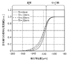
- FIG. 9 is a graph showing simulation results of current spread in the lateral direction (that is, the X-axis direction) of the semiconductor laser device 10 according to the present embodiment.
- FIG. 10 is a graph in which a part of FIG. 9 is enlarged.
- the horizontal axis in FIGS. 9 and 10 indicates the position in the horizontal direction, and the vertical axis indicates the normalized value of the current flowing through the active layer 23 .
- FIG. 11 is a graph showing simulation results of the lateral width of the near-field pattern (NFP) of the semiconductor laser device 10 according to the present embodiment.
- the horizontal axis of FIG. 11 indicates the remaining thickness of the P-type contact layer 25 in the bottom portion 20b, and the vertical axis indicates the width of the NFP in the horizontal direction.
- FIG. 12 is a graph showing simulation results of current spread in the resonance direction (that is, Y-axis direction) of the semiconductor laser device 10 according to the present embodiment.
- the remaining thickness of the P-type contact layer 25 at the bottom 20b of the semiconductor laser device 10 is Tr.
- the remaining thickness of the P-type contact layer 25 is the distance from the lower surface of the P-type contact layer 25 to the bottom portion 20b.
- 9 and 10 show simulation results when the residual thickness Tr of the P-type contact layer 25 is 0 nm, 10 nm, 20 nm, and 30 nm.
- the width of the ridge portion 20r (that is, the dimension in the X-axis direction) was set to 230 ⁇ m, and the entire upper surface of the ridge portion 20r was used as the current injection window region.
- the bottom portion 20b around the ridge portion 20r including the lateral direction, it is possible to suppress the current leaking from the ridge portion 20r in the lateral direction. Further, as the residual thickness of the P-type contact layer 25 is reduced, the current leaking laterally from the ridge portion 20r is reduced. In this embodiment, the P-side semiconductor layer 24 is exposed at the bottom portion 20b. In other words, since the residual thickness of the P-type contact layer 25 is zero, the current leaking laterally from the ridge portion 20r can be minimized. Therefore, according to the semiconductor laser device 10 according to the present embodiment, the reactive current during laser oscillation can be reduced, so that it is possible to improve the light emission efficiency and suppress the decrease in the laser light output.
- a residual thickness Tr of the P-type contact layer 25 at the bottom portion 20b of the semiconductor laser device 10 may be greater than zero. That is, the P-type contact layer 25 may be exposed on the bottom portion 20b.
- the NFP width of the semiconductor laser device 10 is reduced. That is, the NFP width can be reduced by providing the bottom portion 20b around the ridge portion 20r including the lateral direction and reducing the remaining thickness of the P-type contact layer 25.
- the NFP width can be reduced to a value close to the width (230 ⁇ m) of the ridge portion 20r, and the divergence angle of laser light can be suppressed.
- FIG. 12 shows simulation results with and without the P-type contact layer 25 on the bottom portion 20b located between the ridge portion 20r and the end faces 10F and 10R.
- the residual thickness Tr of the P-type contact layer 25 when the P-type contact layer 25 is present on the bottom portion 20b is 50 nm.
- the distance between the ridge portion 20r and the end surfaces 10F and 10R is set to 80 ⁇ m
- the length of the window region 10w (that is, the dimension in the Y-axis direction) is set to 70 ⁇ m.
- the current flowing from the ridge portion 20r to the vicinity of the end surfaces 10F and 10R can be suppressed. Also, by eliminating the P-type contact layer 25 in the bottom portion 20b, the current flowing from the ridge portion 20r to the vicinity of the end surfaces 10F and 10R can be further suppressed.
- the P-side semiconductor layer 24 is exposed at the bottom portion 20b located between the ridge portion 20r and the end surfaces 10F and 10R.
- the semiconductor laser device 10 of the present embodiment since there is no P-type contact layer 25 in the bottom portion 20b located between the ridge portion 20r and the end surfaces 10F and 10R, the current flowing from the ridge portion 20r to the vicinity of the end surfaces 10F and 10R can be minimized. Therefore, according to the semiconductor laser device 10 of the present embodiment, carrier diffusion into the window region 10w formed near the facets 10F and 10R can be suppressed, so that the occurrence of COD can be suppressed. Further, in the present embodiment, since carrier injection into the window region 10w that does not contribute to amplification of laser light can be reduced, light emission efficiency and laser light output can be increased.
- the distance Db from the upper surface of the active layer 23 to the bottom portion 20b may be less than the film thickness of the P-side semiconductor layer 24, like the bottom portion 20b according to the present embodiment. That is, part of the P-side semiconductor layer 24 may be removed at the bottom portion 20b. Thereby, the current flowing from the ridge portion 20r to the vicinity of the end surfaces 10F and 10R can be further suppressed.
- the effective refractive index difference ( ⁇ n) between the inner side and the outer side of the ridge portion 20r increases, as shown in FIG.
- the semiconductor laser element 10 oscillates not as a gain-guided type but as a refractive index-guided type, so that the horizontal divergence angle increases. For this reason, when the semiconductor laser device 10 is used in a system using an optical lens, the light capturing efficiency is lowered. Therefore, the distance Db of the bottom portion 20b inside the resonator is set within a range in which an increase in the effective refractive index difference can be suppressed.
- the distance Db may be set to a value within a range where the change in the effective refractive index difference is small (0.4 ⁇ m or more and 0.6 ⁇ m or less). Further, the distance Db may be set to 0.15 ⁇ m or more so that the effective refractive index difference is 2.0 ⁇ 10 ⁇ 4 or less. This makes it possible to suppress current spread while suppressing an increase in the horizontal spread angle of the laser light.
- the window region 10w in the resonance direction is greater than the length of the bottom portion 20b positioned between the end face 10F and the ridge portion 20r in the resonance direction, the window region 10w is also formed immediately below the ridge portion 20r. . Since the window region 10w positioned directly below the ridge portion 20r is positioned relatively far from the end faces 10F and 10R, the effect of suppressing the generation of COD on the end faces 10F and 10R is not large. In addition, since a relatively large current flows through the window region 10w located directly below the ridge portion 20r, carrier injection into the window region 10w, which does not contribute to amplification of the laser light, increases due to the laser light.
- the length in the resonance direction of the window region 10w may be smaller than the length in the resonance direction of the bottom portion 20b located between the end surface 10F and the ridge portion 20r.
- the length in the resonance direction of the bottom portion 20b located between the end face 10F and the ridge portion 20r may be 80 ⁇ m or more.
- the length of the window region 10w in the resonance direction may be, for example, 70 ⁇ m or more.
- both ends of the pad electrode 50 in the resonance direction are located between the two end faces 10F and 10R and the ridge portion 20r. That is, since the pad electrode 50 is not arranged on the end faces, the mounting stress applied near the end faces 10F and 10R can be reduced when the upper surface of the P-side semiconductor layer 24 is mounted on the mounting base via solder. Moreover, since a portion of the pad electrode 50 is located on the bottom portion 20b near the end surfaces 10F and 10R, the pad electrode 50 can cover the top and side surfaces of the ridge portion 20r and the bottom portion 20b near the ridge portion 20r. As a result, heat generated by Joule heat in the ridge due to current injection and heat generated by non-radiative recombination of carriers can be effectively dissipated through the pad electrode 50 .
- the heat dissipation of the end faces 10F and 10R can be improved.
- the distance between the end of the pad electrode 50 in the resonance direction and the end surfaces 10F and 10R may be 15 ⁇ m or less. Thereby, heat dissipation can be further improved.
- FIGS. 2 and 3 and FIGS. 14 to 23 are schematic cross-sectional views showing each step of the method of manufacturing the semiconductor laser device 10 according to this embodiment.
- 14, 16, 18, 20, and 22 show cross sections of the semiconductor laser device 10 taken along line II-II in FIG. 1 during the manufacturing process.
- 15, 17, 19, 21 and 23 show cross sections of the semiconductor laser device 10 taken along line III-III in FIG. 1 during the manufacturing process.
- an N-side semiconductor layer 22 is formed on the upper surface of a substrate 21, an active layer 23 is formed above the N-side semiconductor layer 22, and a P-side semiconductor layer is formed above the active layer 23. 24 is formed, and a P-type contact layer 25 is formed above the P-side semiconductor layer 24 .
- the N-side semiconductor layer 22, the active layer 23, the P The side semiconductor layer 24 and the P-type contact layer 25 are laminated by sequentially growing crystals.
- an N-type buffer layer 22a, a first N-type compositionally graded layer 22b, an N-type cladding layer 22c, and a second N-type compositionally graded layer 22d are crystal-grown in order on the substrate 21.
- the second P-side barrier layer 23f and the P-type guide layer 23g are sequentially crystal-grown.
- a first P-type compositionally graded layer 24a, a P-type cladding layer 24b, and a second P-type compositionally graded layer 24c are sequentially crystal-grown on the active layer .
- window regions 10w are formed near the end faces 10F and 10R. Specifically, window regions 10w are formed in the end surfaces 10F and 10R of the semiconductor stacked body 10S.
- a method of forming the window region 10w there are generally an impurity diffusion method and a hole diffusion method.
- windows are formed by a hole diffusion method. This is because it is important to reduce the amount of light absorption by reducing the loss in the ultra-high output semiconductor laser device 10 that exceeds 10 W per emitter.
- the window region 10w is formed by the impurity diffusion method, the light absorption increases due to the impurities, making it difficult to reduce the light absorption loss.
- the hole diffusion method does not use impurities, the light absorption loss caused by the introduction of impurities can be reduced by forming the window region 10w by the hole diffusion method.
- the window region 10w can be formed by subjecting the semiconductor laminate 10S to a rapid high temperature treatment. For example, after a protective film that generates Ga vacancies during high-temperature treatment is formed on the semiconductor laminate 10S in the region where the window region is formed, it is exposed to extremely high heat of 750° C. or more and 950° C. or less near the crystal growth temperature. By further diffusing the Ga vacancies, the quantum well structure of the active layer 23 can be disordered and made windowed (transparent) by interdiffusion between the vacancies and the group III element. As a result, the bandgap of the active layer 23 can be increased, and the region in which the quantum well structure is disordered can function as the window region 10w.
- the window region 10w is formed by the hole diffusion method in the present embodiment, it may be formed by another method such as an impurity diffusion method.
- recesses are formed in the P-type contact layer 25 to define the ridge portion 20r and the wing portions 20w.
- the bottom surface of the formed concave portion is the bottom portion 20b.
- a mask made of SiO 2 or the like is formed in a predetermined pattern on the P-type contact layer 25 by photolithography, and then recesses are formed by wet etching to form the ridge 20r and the A wing portion 20w is formed.
- a bottom portion 20b is formed instead of the ridge portion 20r.
- recesses may be formed at the positions where the separation grooves 20t for individualization are formed at both ends of the semiconductor laser element 10 in the X-axis direction. The recess extends in the resonance direction.
- separation grooves 20t having inclined surfaces are formed at both ends of the semiconductor stacked body 10S in the X-axis direction.
- a mask made of SiO 2 or the like is formed in a predetermined pattern on the P-side semiconductor layer 24 by photolithography, and then wet etching is performed to remove the N-side semiconductor from the P-side semiconductor layer 24 .
- wet etching is performed to remove the N-side semiconductor from the P-side semiconductor layer 24 .
- the separation groove 20t is a groove used when singulating the semiconductor laser element 10, and extends in the resonance direction.
- a sulfuric acid-based etchant for example, can be used as an etchant for forming the separation grooves 20t.
- the etching liquid is not limited to the sulfuric acid-based etching liquid, and may be an organic acid-based etching liquid or an ammonia-based etching liquid.
- the separation groove 20t is formed by isotropic wet etching. This makes it possible to form a constricted structure (that is, an overhang structure) in the plurality of semiconductor layers by forming inclined surfaces on the side surfaces of the plurality of semiconductor layers.
- the inclination angle of the side surface of the separation groove 20t differs according to the Al composition ratio of the AlGaAs material of each layer constituting the plurality of semiconductor layers.
- the etching rate can be increased by increasing the Al composition ratio of the AlGaAs material. Therefore, in order to form the inclined side surfaces of the semiconductor stacked body 10S as shown in FIGS. , the etching rate in the lateral direction (X-axis direction) of the P-side semiconductor layer 24 can be maximized. As a result, the narrowest portion (the narrowest portion in the horizontal direction) of the semiconductor stacked body 10S can be formed in the vicinity of the P-side semiconductor layer 24 .
- a SiN film is formed as an insulating film 30 on the entire upper surface of the substrate 21 as shown in FIGS. accumulate. After that, using photolithography technology and etching technology, the insulating film 30 is removed from a portion corresponding to the current injection window 25a to form an opening 30a. Note that the insulating film 30 is not removed from the portions corresponding to the current non-injection regions.
- the etching of the insulating film 30 wet etching using a hydrofluoric acid-based etchant or dry etching by reactive ion etching (RIE) can be used.
- the insulating film 30 is a SiN film, it is not limited to this, and may be a SiO 2 film or the like.
- plasma-enhanced chemical vapor deposition hereinafter referred to as PCVD
- Mixed gases such as SiH 4 , CF 4 , NH 3 , N 2 O, and N 2 can be used as source gases for forming the insulating film 30 .
- the film forming technique is the PCVD method, and a mixed gas of SiH 4 , NH 3 and N 2 is used as the material gas.
- the volume content of SiH 4 in the mixed gas is 5% or more and 18% or less
- the temperature of the lower electrode on which the semiconductor substrate is placed is 150° C. or more and 350° C. or less
- the pressure in the chamber is 50 Pa or more and 200 Pa or less.
- the RF power can be 100 W or more and 400 W or less, but it is not limited to this and may be selected as appropriate.
- the surface of the bottom portion 20b is less likely to be oxidized because the source gas does not contain O.sub.2 .
- a SiO 2 film is used as the insulating film 30
- a mixed gas of SiH 4 , N 2 O, and N 2 is used as the material gas.
- a P-side electrode is formed on the semiconductor laminate 10S.
- a first P-side electrode 41, a pad electrode 50, and a second P-side electrode 42 are formed in this order on the P-type contact layer 25 as P-side electrodes.
- the first P-side electrode 41 made of a laminated film of a Ti film, a Pt film and an Au film is formed as a base electrode by an electron beam vapor deposition method.
- a pad electrode 50 made of an Au plating film is formed by electroplating.
- the pad electrode 50 near the end surface is selectively removed using photolithography technology, etching technology, and lift-off technology.
- An iodine solution can be used as an etchant for etching the pad electrode 50 made of the Au plating film.
- a second P-side electrode 42 made of a laminated film of a Ti film, a Pt film and an Au film is formed on the pad electrode 50 by electron beam evaporation.
- the first P-side electrode 41 and the second P-side electrode 42 are formed over substantially the entire length in the resonance direction, but the pad electrode 50 is not formed near the end surfaces 10F and 10R.
- an N-side electrode 60 is formed on the lower main surface of the substrate 21 .
- the N-side electrode 60 is formed by sequentially forming an AuGe film, a Ni film, an Au film, a Ti film, a Pt film, and an Au film from the substrate 21 side.
- the substrate 21 on which the semiconductor laminate 10S is formed is separated into bars by dicing or cleavage using a blade, and then the chips are separated by cutting using the separation grooves 20t as cutting portions. conduct. As a result, individual pieces of the semiconductor laser device 10 can be manufactured.
- semiconductor laser devices 10 according to modified examples 1 to 8 will be described.
- the semiconductor laser devices according to Modifications 1 to 3 have the same semiconductor layered body 10S as the semiconductor laser device 10 according to the embodiment, but the semiconductor layered body 10S is partially different in layer configuration.
- the semiconductor laser devices according to Modifications 4 to 8 differ from the semiconductor laser device 10 according to the embodiment in the configuration of the ridge portion 20r, the wing portions 20w, and the bottom portion 20b of the semiconductor laminate 10S.
- the configuration different from the semiconductor laser device 10 according to the embodiment will be mainly described.
- the first N-type composition gradient layer 22b of the semiconductor laser device according to Modification 1 is an N-type Al x1 Ga 1-x1 As layer with a thickness of 0.05 ⁇ m.
- the Al composition ratio x1 of the first N-type composition gradient layer 22b is 0.15 near the interface with the N-type buffer layer 22a and 0.353 near the interface with the N-type cladding layer 22c. increases as it approaches the N-type cladding layer 22c.
- the N-type cladding layer 22c of the semiconductor laser device according to Modification 1 is an N-type Al 0.353 Ga 0.647 As layer with a thickness of 2.40 ⁇ m.
- the second N-type compositionally graded layer 22d of the semiconductor laser device according to Modification 1 is an N-type Al x2 Ga 1-x2 As layer with a thickness of 0.03 ⁇ m.
- the Al composition ratio x2 of the second N-type composition gradient layer 22d is 0.353 in the vicinity of the interface with the N-type cladding layer 22c and 0.323 in the vicinity of the interface with the active layer 23. It becomes smaller as the layer 23 is approached.
- the N-type guide layer 23a of the semiconductor laser device according to Modification 1 is an N-type Al 0.323 Ga 0.677 As layer with a thickness of 0.95 ⁇ m.
- the second N-side barrier layer 23b of the semiconductor laser device according to Modification 1 has an N-type layer arranged above the N-type guide layer 23a and an undoped layer arranged above the N-type layer.
- the N-type layer is an N-type Al 0.18 Ga 0.82 As layer with a thickness of 0.0250 ⁇ m.
- the N-type layer is doped with silicon as an impurity.
- the undoped layer is an Al 0.18 Ga 0.82 As layer with a thickness of 0.0065 ⁇ m.
- the first N-side barrier layer 23c of the semiconductor laser device according to Modification 1 is an undoped Al 0.35 Ga 0.55 In 0.10 As layer with a thickness of 0.0035 ⁇ m.
- the well layer 23d of the semiconductor laser device according to Modification 1 is an undoped In 0.11 Ga 0.89 As layer with a thickness of 0.0060 ⁇ m.
- the first P-side barrier layer 23e of the semiconductor laser device according to Modification 1 is an undoped Al 0.35 Ga 0.55 In 0.10 As layer with a thickness of 0.0035 ⁇ m.
- the second P-side barrier layer 23f of the semiconductor laser device according to Modification 1 has an undoped layer arranged above the first P-side barrier layer 23e and a P-type layer arranged above the undoped layer.
- the undoped layer is an Al 0.18 Ga 0.82 As layer with a thickness of 0.0065 ⁇ m.
- the P-type layer is a P-type Al 0.18 Ga 0.82 As layer with a thickness of 0.025 ⁇ m.
- the P-type layer is doped with carbon (C) as an impurity.
- the P-type guide layer 23g of the semiconductor laser device according to Modification 1 is a P-type Al 0.32 Ga 0.68 As layer with a thickness of 0.1825 ⁇ m.
- the first P-type compositionally graded layer 24a of the semiconductor laser device according to Modification 1 is a P-type Al y1 Ga 1-y1 As layer with a thickness of 0.05 ⁇ m.
- the Al composition ratio y1 of the first P-type composition gradient layer 24a is 0.32 near the interface with the active layer 23 and 0.70 near the interface with the P-type cladding layer 24b. It becomes larger as it approaches the mold cladding layer 24b.
- the semiconductor laser device according to Modification 1 having the configuration described above also exhibits the same effect as the semiconductor laser device 10 according to the embodiment. According to the semiconductor laser device according to Modification 1, laser light in the wavelength band of 915 nm can be obtained.
- the N-type buffer layer 22a of the semiconductor laser device according to Modification 2 is an N-type GaAs layer with a thickness of 0.10 ⁇ m.
- the first N-type composition gradient layer 22b of the semiconductor laser device according to Modification 2 is an N-type Al x1 Ga 1-x1 As layer with a thickness of 0.05 ⁇ m.
- the Al composition ratio x1 of the first N-type composition gradient layer 22b is 0.15 near the interface with the N-type buffer layer 22a and 0.25 near the interface with the N-type cladding layer 22c. increases as it approaches the N-type cladding layer 22c.
- the N-type cladding layer 22c of the semiconductor laser device according to Modification 2 is an N-type Al 0.25 Ga 0.75 As layer with a thickness of 1.80 ⁇ m.
- the N-side semiconductor layer 22 of the semiconductor laser device according to Modification 2 does not have the second N-type composition gradient layer 22d.
- the N-type guide layer 23a of the active layer 23 of the semiconductor laser device according to Modification 2 includes a third N-type guide layer, a second N-type guide layer disposed above the third N-type guide layer, and It has a first N-type guide layer positioned above the second N-type guide layer.
- the third N-type guide layer is an N-type Al 0.25 Ga 0.75 As layer with a thickness of 0.20 ⁇ m.
- the second N-type guide layer is an N-type Al 0.23 Ga 0.77 As layer with a thickness of 0.60 ⁇ m.
- the first N-type guide layer is an N-type Al 0.21 Ga 0.79 As layer with a thickness of 0.46 ⁇ m.
- the second N-side barrier layer 23b of the semiconductor laser device according to Modification 2 has an N-type layer arranged above the N-type guide layer 23a and an undoped layer arranged above the N-type layer.
- the N-type layer is an N-type Al 0.16 Ga 0.84 As layer with a thickness of 0.0268 ⁇ m.
- the N-type layer is doped with silicon as an impurity.
- the undoped layer is an Al 0.16 Ga 0.84 As layer with a thickness of 0.0083 ⁇ m.
- the second P-side barrier layer 23f of the semiconductor laser device according to Modification 2 is an Al 0.16 Ga 0.84 As layer with a thickness of 0.0083 ⁇ m.
- the P-type guide layer 23g of the semiconductor laser device according to Modification 2 is a P-type Al z1 Ga 1-z1 As layer with a thickness of 0.29 ⁇ m.
- the Al composition ratio x1 of the P-type guide layer 23g is 0.19 in the vicinity of the interface with the second P-side barrier layer 23f and 0.21 in the vicinity of the interface with the P-side semiconductor layer 24. It becomes larger as it approaches the P-side semiconductor layer 24 .
- the first P-type compositionally graded layer 24a of the semiconductor laser device according to Modification 2 is a P-type Al y1 Ga 1-y1 As layer with a thickness of 0.05 ⁇ m.
- the Al composition ratio y1 of the first P-type composition gradient layer 24a is 0.21 near the interface with the active layer 23, 0.70 near the interface with the P-type cladding layer 24b, and the stacking direction position is P It becomes larger as it approaches the mold cladding layer 24b.
- the P-type cladding layer 24b of the semiconductor laser device according to Modification 2 is a P-type Al 0.70 Ga 0.30 As layer with a thickness of 0.70 ⁇ m.
- the semiconductor laser device according to Modification 2 having the configuration described above also exhibits the same effect as the semiconductor laser device 10 according to the embodiment.
- the N-type buffer layer 22a of the semiconductor laser device according to Modification 3 is an N-type GaAs layer with a thickness of 0.10 ⁇ m.
- the first N-type composition gradient layer 22b of the semiconductor laser device according to Modification 3 is an N-type Al x1 Ga 1-x1 As layer with a thickness of 0.05 ⁇ m.
- the Al composition ratio x1 of the first N-type composition gradient layer 22b is 0.15 near the interface with the N-type buffer layer 22a and 0.24 near the interface with the N-type cladding layer 22c. increases as it approaches the N-type cladding layer 22c.
- the N-type cladding layer 22c of the semiconductor laser device according to Modification 3 is an N-type Al 0.24 Ga 0.76 As layer with a thickness of 1.80 ⁇ m.
- the second N-type compositionally graded layer 22d of the semiconductor laser device according to Modification 3 is an N-type Al x2 Ga 1-x2 As layer with a thickness of 1.00 ⁇ m.
- the Al composition ratio x2 of the second N-type composition gradient layer 22d is 0.24 in the vicinity of the interface with the N-type cladding layer 22c and 0.22 in the vicinity of the interface with the active layer 23. It becomes smaller as the layer 23 is approached.
- the N-type guide layer 23a of the semiconductor laser device according to Modification 3 has a second N-type guide layer and a first N-type guide layer arranged above the second N-type guide layer.
- the second N-type guide layer is an N-type Al z2 Ga 1-z2 As layer with a thickness of 0.40 ⁇ m.
- the Al composition ratio z2 of the second N-type guide layer is 0.22 in the vicinity of the interface with the N-side semiconductor layer 22 and 0.19 in the vicinity of the interface with the first N-side guide layer. It becomes smaller as it approaches the first N-side guide layer.
- the first N-type guide layer is an N-type Al 0.19 Ga 0.81 As layer with a thickness of 0.09 ⁇ m.
- the second N-side barrier layer 23b of the semiconductor laser device according to Modification 3 has an N-type layer arranged above the N-type guide layer 23a and an undoped layer arranged above the N-type layer.
- the N-type layer is an N-type Al 0.16 Ga 0.84 As layer with a thickness of 0.0268 ⁇ m.
- the N-type layer is doped with silicon as an impurity.
- the undoped layer is an Al 0.16 Ga 0.84 As layer with a thickness of 0.0083 ⁇ m.
- the second P-side barrier layer 23f of the semiconductor laser device according to Modification 3 is an Al 0.16 Ga 0.84 As layer with a thickness of 0.0083 ⁇ m.
- the P-type guide layer 23g of the semiconductor laser device according to Modification 3 has a first P-type guide layer and a second P-type guide layer arranged above the first P-type guide layer.
- the first P-type guide layer is a P-type Al 0.19 Ga 0.81 As layer with a thickness of 0.01 ⁇ m.
- the second P-type guide layer is a P-type Al z1 Ga 1-z1 As layer with a thickness of 0.28 ⁇ m.
- the Al composition ratio z1 of the second P-type guide layer is 0.19 in the vicinity of the interface with the first P-side guide layer, 0.21 in the vicinity of the interface with the P-side semiconductor layer 24, and the stacking direction position is It becomes larger as it approaches the P-side semiconductor layer 24 .
- the first P-type compositionally graded layer 24a of the semiconductor laser device according to Modification 3 is a P-type Al y1 Ga 1-y1 As layer with a thickness of 0.05 ⁇ m.
- the Al composition ratio y1 of the first P-type composition gradient layer 24a is 0.21 near the interface with the active layer 23, 0.70 near the interface with the P-type cladding layer 24b, and the stacking direction position is P It becomes larger as it approaches the mold cladding layer 24b.
- the P-type cladding layer 24b of the semiconductor laser device according to Modification 3 is a P-type Al 0.70 Ga 0.30 As layer with a thickness of 0.70 ⁇ m.
- the semiconductor laser device according to Modification 3 having the configuration described above also exhibits the same effect as the semiconductor laser device 10 according to the embodiment.
- FIG. 24 is a schematic plan view showing the overall configuration of a semiconductor laser device 110 according to Modification 4.
- the semiconductor laser device 110 according to Modification 4 differs from the semiconductor laser device 10 according to the embodiment in that it does not have wing portions 20w.
- the region where the wing portions 20w are arranged in the semiconductor laser device 10 according to the embodiment is replaced with the bottom portion 20b in the semiconductor laser device according to the fourth modification.
- the semiconductor laser device 110 according to Modification Example 4 having the configuration described above also exhibits the same effects as the semiconductor laser device 10 according to the embodiment, except for the effects of the wing portions 20w.
- FIG. 25 is a schematic plan view showing the overall configuration of a semiconductor laser device 210 according to Modification 5. As shown in FIG. As shown in FIG. 25, the semiconductor laser device 210 according to Modification 5 differs from the semiconductor laser device 10 according to the embodiment in that the bottom portion 20b is provided laterally outside the wing portions 20w.
- the semiconductor laser device 210 according to Modification 5 having the configuration described above also exhibits the same effect as the semiconductor laser device 10 according to the embodiment. Furthermore, according to the semiconductor laser element 210 according to Modification 5, the bottom portions 20b are arranged on both sides of the wing portions 20w in the lateral direction, so that the adhesion of the insulating film 30 to the semiconductor stacked body 10S can be enhanced. .
- FIG. 26 is a schematic plan view showing the overall configuration of a semiconductor laser device 310 according to Modification 6.
- the bottom portion 20b surrounds the wing portions 20w. That is, the bottom portion 20b is arranged laterally outside the wing portion 20w and between the wing portion 20w and the end surfaces 10F and 10R.
- the wing portions 20w are separated from the end surfaces 10F and 10R. Also, each distance from the wing portion 20w to the end surfaces 10F and 10R may be greater than each distance from the ridge portion 20r to the end surfaces 10F and 10R.
- the semiconductor laser device 310 according to Modification Example 6 having the configuration described above also exhibits the same effect as the semiconductor laser device 10 according to the embodiment. Furthermore, according to the semiconductor laser element 310 according to Modification 6, the bottom portion 20b is arranged around the wing portion 20w, so that the adhesion of the insulating film 30 to the semiconductor stacked body 10S can be enhanced.
- FIG. 27 is a schematic plan view showing the overall configuration of a semiconductor laser device 410 according to Modification 7.
- the semiconductor laser device 410 according to Modification Example 7 differs from the semiconductor laser device 10 according to the embodiment in that dummy ridge portions 420r are arranged between the ridge portion 20r and the end faces 10F and 10R. do.
- the dummy ridge portion 420r is a portion that protrudes upward from the bottom portion 20b similarly to the ridge portion 20r.
- the dummy ridge portion 420r is adjacent to the ridge portion 20r via the bottom portion 20b.
- the height of the dummy ridge portion 420r from the bottom portion 20b is equal to the height of the ridge portion 20r from the bottom portion 20b.
- the width of the dummy ridge portion 420r (that is, the dimension in the X-axis direction) is equal to the width of the ridge portion 20r, and has a rectangular shape when viewed from above.
- the dummy ridge portion 420r is in contact with the end surface 10F or 10R.
- the semiconductor laser device 410 according to Modification Example 7 having the configuration described above also exhibits the same effect as the semiconductor laser device 10 according to the embodiment. Furthermore, according to the semiconductor laser device according to Modification 7, by providing the dummy ridge portion 420r, stress applied to the semiconductor laser device 410 when the semiconductor laser device 10 is mounted, for example, is dispersed to the dummy ridge portion 420r. Therefore, it is possible to suppress concentration of stress only on the ridge portion 20r. Therefore, it is possible to prevent the ridge portion 20r from being damaged.
- the insulating film 30 is likely to peel off in the region where the insulating film 30 is in contact with the bottom portion 20b because the adhesion between the insulating film 30 and the bottom portion 20b is poor.
- the semiconductor laser device 410 according to Modification 7 since a part of the region where the AlGaAs layer is exposed between the facets 10F and 10R and the ridge portion 20r can be replaced with the dummy ridge portion 420r made of GaAs, insulation is achieved. Adhesion between the film 30 and the semiconductor stack 10S can be enhanced.
- FIGS. 28 and 29 are a schematic plan view and a cross-sectional view, respectively, showing the overall configuration of a semiconductor laser device 510 according to Modification 8.
- FIG. 29 shows a cross section along line XXIX-XXIX near the end face 10F in FIG.
- dummy ridge portions 520r are arranged between the ridge 20r and the end surfaces 10F and 10R, as in Modification 7. is different from the semiconductor laser device 10 according to the embodiment.
- the dummy ridge portion 520r according to Modification 8 is integrated with the wing portion 20w.
- the regions adjacent to the end faces 10F and 10R of the bottom portion 20b between the dummy ridge portion 420r and the wing portion 20w according to Modification 7 are replaced with the dummy ridge portion 520r. That is, the bottom portion 20b does not contact the end surfaces 10F and 10R (see FIG. 29).
- the semiconductor laser device according to Modification Example 8 having the configuration described above also exhibits the same effect as the semiconductor laser device 10 according to the embodiment. Furthermore, according to the semiconductor laser device according to Modification 8, by providing the dummy ridge portion 520r, stress applied to the semiconductor laser device 510 when the semiconductor laser device 10 is mounted, for example, is dispersed to the dummy ridge portion 520r. Therefore, it is possible to suppress concentration of stress only on the ridge portion 20r. Therefore, it is possible to prevent the ridge portion 20r from being damaged.
- the insulating film 30 is likely to peel off in the region where the insulating film 30 is in contact with the bottom portion 20b because the adhesion between the insulating film 30 and the bottom portion 20b is poor.
- the semiconductor laser device 410 according to Modification 7 since a part of the region where the AlGaAs layer is exposed between the facets 10F and 10R and the ridge portion 20r can be replaced with the dummy ridge portion 520r made of GaAs, insulation is achieved. Adhesion between the film 30 and the semiconductor stack 10S can be enhanced.
- the semiconductor laser device 510 according to Modification 8 since the bottom portion 20b does not come into contact with the end surfaces 10F and 10R, the contact surface between the insulating film 30 with poor adhesion and the bottom portion 20b is not exposed from the end surfaces 10F and 10R. Therefore, peeling of the insulating film 30 can be further suppressed.
- the distance Db from the upper surface of the active layer 23 of the bottom portion 20b may be equal to or greater than the film thickness of the P-side semiconductor layer 24 or less than the film thickness of the P-side semiconductor layer 24. may be In other words, the P-type contact layer 25 or the P-side semiconductor layer 24 may be exposed at the bottom portion 20b.
- the semiconductor laser device and the like of the present disclosure can be applied, for example, as a light source for processing machines as a highly efficient light source.
Landscapes
- Physics & Mathematics (AREA)
- Condensed Matter Physics & Semiconductors (AREA)
- General Physics & Mathematics (AREA)
- Electromagnetism (AREA)
- Optics & Photonics (AREA)
- Geometry (AREA)
- Semiconductor Lasers (AREA)
Abstract
Description
実施の形態に係る半導体レーザ素子について説明する。
本実施の形態に係る半導体レーザ素子の全体構成について図1~図4を用いて説明する。図1は、本実施の形態に係る半導体レーザ素子10の全体構成を示す模式的な平面図である。図2~図4は、本実施の形態に係る半導体レーザ素子10の全体構成を示す模式的な断面図である。図2、図3、及び図4には、それぞれ、図1のII-II線、III-III線、及びIV-IV線における断面が示されている。なお、各図には、互いに直交するX軸、Y軸、及びZ軸が示されている。X軸、Y軸、及びZ軸は、右手系の直交座標系である。半導体レーザ素子10の積層方向は、Z軸方向に平行であり、光(本実施の形態では、レーザ光)の主な出射方向は、Y軸方向に平行である。
本実施の形態に係る半導体レーザ素子10による効果について説明する。上述したとおり、本実施の形態に係る半導体レーザ素子10は、リッジ部20rを有する半導体積層体10Sを備え、図1に示されるように、底部20bは、リッジ部20rの周囲を取り囲む。また、底部20bにおいて、P側半導体層24が露出している。本実施の形態に係るこれらの構成による効果について、図8~図12を用いて説明する。図8は、本実施の形態に係る半導体レーザ素子10のシミュレーションにおいて用いたモデルの構造を示す断面図である。図9は、本実施の形態に係る半導体レーザ素子10の横方向(つまり、X軸方向)における電流拡がりのシミュレーション結果を示すグラフである。図10は、図9の一部を拡大したグラフである。図9及び図10の横軸は、横方向の位置を示し、縦軸は活性層23に流れる電流値を規格化した値を示す。図11は、本実施の形態に係る半導体レーザ素子10のニアフィールドパターン(NFP)の横方向の幅のシミュレーション結果を示すグラフである。図11の横軸は、底部20bにおけるP型コンタクト層25の残厚を示し、縦軸は、横方向におけるNFP幅を示す。図12は、本実施の形態に係る半導体レーザ素子10の共振方向(つまり、Y軸方向)における電流拡がりのシミュレーション結果を示すグラフである。
本実施の形態に係る半導体レーザ素子10の製造方法について、図2及び図3、並びに図14~図23を用いて説明する。図14~図23は、本実施の形態に係る半導体レーザ素子10の製造方法の各工程を示す模式的な断面図である。図14、図16、図18、図20、及び図22には、製造過程における半導体レーザ素子10の図1のII-II線における断面が示されている。図15、図17、図19、図21及び図23には、製造過程における半導体レーザ素子10の図1のIII-III線における断面が示されている。
変形例1~変形例8に係る半導体レーザ素子10について説明する。変形例1~変形例3に係る半導体レーザ素子は、実施の形態に係る半導体レーザ素子10と同様の半導体積層体10Sを有するが、半導体積層体10Sの一部の層構成が異なる。変形例4~変形例8に係る半導体レーザ素子は、半導体積層体10Sのリッジ部20r、ウイング部20w、及び底部20bの構成において、実施の形態に係る半導体レーザ素子10と異なる。以下、変形例1~変形例8に係る半導体レーザ素子の構成のうち、実施の形態に係る半導体レーザ素子10と異なる構成を中心に説明する。
変形例1に係る半導体レーザ素子の構成について説明する。
変形例2に係る半導体レーザ素子の構成について説明する。
変形例3に係る半導体レーザ素子の構成について説明する。
変形例4に係る半導体レーザ素子について図24を用いて説明する。図24は、変形例4に係る半導体レーザ素子110の全体構成を示す模式的な平面図である。図24に示されるように、変形例4に係る半導体レーザ素子110は、ウイング部20wを有さない点において、実施の形態に係る半導体レーザ素子10と相違する。実施の形態に係る半導体レーザ素子10においてウイング部20wが配置されている領域は、変形例4に係る半導体レーザ素子では、底部20bに代えられている。
変形例5に係る半導体レーザ素子について図25を用いて説明する。図25は、変形例5に係る半導体レーザ素子210の全体構成を示す模式的な平面図である。図25に示されるように、変形例5に係る半導体レーザ素子210は、ウイング部20wの横方向における外側に底部20bを有する点において、実施の形態に係る半導体レーザ素子10と相違する。
変形例6に係る半導体レーザ素子について図26を用いて説明する。図26は、変形例6に係る半導体レーザ素子310の全体構成を示す模式的な平面図である。図26に示されるように、変形例6に係る半導体レーザ素子310においては、底部20bはウイング部20wの周囲を取り囲む。つまり、ウイング部20wの横方向における外側、及び、ウイング部20wと端面10F及び10Rとの間に底部20bが配置される。変形例6では、ウイング部20wは、端面10F及び10Rから離間している。また、ウイング部20wから端面10F及び10Rまでの各距離は、リッジ部20rから端面10F及び10Rまでの各距離より大きくてもよい。
変形例7に係る半導体レーザ素子について図27を用いて説明する。図27は、変形例7に係る半導体レーザ素子410の全体構成を示す模式的な平面図である。変形例7に係る半導体レーザ素子410は、リッジ部20rと、端面10F及び10Rとの間の各々に、ダミーリッジ部420rが配置されている点において、実施の形態に係る半導体レーザ素子10と相違する。ダミーリッジ部420rは、リッジ部20rと同様に底部20bから上方に向かって突出する部分である。ダミーリッジ部420rは、底部20bを介してリッジ部20rと隣り合う。変形例7では、ダミーリッジ部420rの底部20bからの高さは、リッジ部20rの底部20bからの高さと等しい。また、ダミーリッジ部420rの幅(つまり、X軸方向の寸法)は、リッジ部20rの幅と等しく、上面視において矩形状の形状を有する。ダミーリッジ部420rは、端面10F又は10Rと接する。
変形例8に係る半導体レーザ素子について図28及び図29を用いて説明する。図28及び図29は、それぞれ、変形例8に係る半導体レーザ素子510の全体構成を示す模式的な平面図及び断面図である。図29には、図28の端面10F付近のXXIX-XXIX線における断面が示されている。図28及び図29に示されるように、変形例8に係る半導体レーザ素子510は、リッジ部20rと、端面10F及び10Rとの間の各々に、変形例7と同様にダミーリッジ部520rが配置されている点において、実施の形態に係る半導体レーザ素子10と相違する。また変形例8に係るダミーリッジ部520rは、ウイング部20wと一体化されている。言い換えると、変形例7に係るダミーリッジ部420rとウイング部20wとの間の底部20bの端面10F及び10Rに隣接する領域がダミーリッジ部520rに置き換えられている。つまり、底部20bは端面10F及び10Rと接しない(図29参照)。
以上、本開示に係る半導体レーザ素子について、各実施の形態に基づいて説明したが、本開示は、上記各実施の形態に限定されるものではない。
10F、10R 端面
10S 半導体積層体
10w 窓領域
20b 底部
20r リッジ部
20t 分離溝
20w ウイング部
21 基板
22 N側半導体層
22a N型バッファ層
22b 第一N型組成傾斜層
22c N型クラッド層
22d 第二N型組成傾斜層
23 活性層
23a N型ガイド層
23b 第二N側バリア層
23c 第一N側バリア層
23d 井戸層
23e 第一P側バリア層
23f 第二P側バリア層
23g P型ガイド層
24 P側半導体層
24a 第一P型組成傾斜層
24b P型クラッド層
24c 第二P型組成傾斜層
25 P型コンタクト層
25a 電流注入窓
30 絶縁膜
30a 開口部
41 第一P側電極
42 第二P側電極
50 パッド電極
60 N側電極
71 第一端面コート膜
72 第二端面コート膜
420r、520r ダミーリッジ部
Claims (12)
- マルチ横モードのレーザ光を出射する半導体レーザ素子であって、
基板と、
前記基板の上方に配置される半導体積層体とを備え、
前記半導体積層体は、
前記基板の上方に配置されるN側半導体層と、
前記N側半導体層の上方に配置される活性層と、
前記活性層の上方に配置されるP側半導体層と、
前記P側半導体層の上方に配置されるP型コンタクト層とを有し、
前記半導体積層体は、互いに対向する二つの端面を有し、
前記レーザ光は、前記二つの端面の間で共振し、
前記半導体積層体は、前記レーザ光の共振方向に延在するリッジ部と、前記半導体積層体の上面の一部であって、前記半導体積層体の上面視において、前記リッジ部の周囲を取り囲む底部とを有し、
前記リッジ部は、前記底部から上方に向かって突出し、
前記リッジ部は、前記二つの端面から離間し、
前記リッジ部は、前記P型コンタクト層の少なくとも一部を含み、
前記半導体積層体の上面のうち、前記リッジ部上のみに、電流が注入される領域である電流注入窓が形成され、
前記活性層の上面から前記底部までの距離は、一様である
半導体レーザ素子。 - 前記底部には、前記P側半導体層が露出している
請求項1に記載の半導体レーザ素子。 - マルチ横モードのレーザ光を出射する半導体レーザ素子であって、
基板と、
前記基板の上方に配置される半導体積層体とを備え、
前記半導体積層体は、
前記基板の上方に配置されるN側半導体層と、
前記N側半導体層の上方に配置される活性層と、
前記活性層の上方に配置されるP側半導体層と、
前記P側半導体層の上方に配置されるP型コンタクト層とを有し、
前記半導体積層体は、互いに対向する二つの端面を有し、
前記レーザ光は、前記二つの端面の間で共振し、
前記半導体積層体は、前記レーザ光の共振方向に延在するリッジ部と、前記半導体積層体の上面の一部であって、前記半導体積層体の上面視において、前記リッジ部の周囲を取り囲む底部と、を有し、
前記リッジ部は、前記底部から上方に向かって突出し、
前記リッジ部は、前記二つの端面から離間し、
前記リッジ部は、前記P型コンタクト層の少なくとも一部を含み、
前記半導体積層体の上面のうち、前記リッジ部上のみに、電流が注入される領域である電流注入窓が形成され、
前記底部には、前記P型コンタクト層が露出している
半導体レーザ素子。 - 前記半導体積層体は、前記P型コンタクト層の一部を含み、かつ、前記共振方向に延在する二つのウイング部を有し、
前記リッジ部の少なくとも一部は、前記半導体積層体の上面視において、前記二つのウイング部の間に配置され、
前記二つのウイング部の各々は、前記底部を介して前記リッジ部と隣り合い、
前記二つのウイング部は、前記底部から上方に向かって突出し、
前記二つのウイング部の前記底部からの高さは、前記リッジ部の前記底部からの高さと等しい
請求項1~3のいずれか1項に記載の半導体レーザ素子。 - 前記二つのウイング部の各々は、前記二つの端面まで延在する
請求項4に記載の半導体レーザ素子。 - 前記半導体積層体は、前記二つの端面のうち前記レーザ光を出射する端面であるフロント端面に隣接する窓領域を有し、
前記窓領域における前記活性層のバンドギャップエネルギーは、前記窓領域以外の領域における前記活性層のバンドギャップエネルギーより大きい
請求項1~5のいずれか1項に記載の半導体レーザ素子。 - 前記窓領域以外の領域における前記活性層は、量子井戸構造を有する
請求項6に記載の半導体レーザ素子。 - 前記窓領域は、前記フロント端面に接し、
前記窓領域の前記共振方向の長さは、前記フロント端面と前記リッジ部との間に位置する前記底部の前記共振方向の長さより小さい
請求項6又は7に記載の半導体レーザ素子。 - 前記半導体積層体の上方に配置される絶縁膜をさらに備え、
前記絶縁膜は、前記電流注入窓に対応する領域に開口部を有する
請求項1~8のいずれか1項に記載の半導体レーザ素子。 - 前記底部における酸素濃度は、前記半導体積層体の内部の酸素濃度より高い
請求項1~9のいずれか1項に記載の半導体レーザ素子。 - 前記P型コンタクト層に接するP側電極と、前記P側電極の上方に配置されるパッド電極とをさらに備え、
前記パッド電極の前記共振方向の両端は、それぞれ前記二つの端面と前記リッジ部との間に位置する
請求項1~10のいずれか1項に記載の半導体レーザ素子。 - 前記半導体レーザ素子の導波特性は、利得導波型である
請求項1~11のいずれか1項に記載の半導体レーザ素子。
Priority Applications (3)
| Application Number | Priority Date | Filing Date | Title |
|---|---|---|---|
| CN202180091975.8A CN116746012A (zh) | 2021-01-29 | 2021-12-22 | 半导体激光器元件 |
| JP2022578164A JPWO2022163237A1 (ja) | 2021-01-29 | 2021-12-22 | |
| US18/358,610 US20230387662A1 (en) | 2021-01-29 | 2023-07-25 | Semiconductor laser element |
Applications Claiming Priority (2)
| Application Number | Priority Date | Filing Date | Title |
|---|---|---|---|
| US202163143463P | 2021-01-29 | 2021-01-29 | |
| US63/143,463 | 2021-01-29 |
Related Child Applications (1)
| Application Number | Title | Priority Date | Filing Date |
|---|---|---|---|
| US18/358,610 Continuation US20230387662A1 (en) | 2021-01-29 | 2023-07-25 | Semiconductor laser element |
Publications (1)
| Publication Number | Publication Date |
|---|---|
| WO2022163237A1 true WO2022163237A1 (ja) | 2022-08-04 |
Family
ID=82654378
Family Applications (1)
| Application Number | Title | Priority Date | Filing Date |
|---|---|---|---|
| PCT/JP2021/047705 WO2022163237A1 (ja) | 2021-01-29 | 2021-12-22 | 半導体レーザ素子 |
Country Status (4)
| Country | Link |
|---|---|
| US (1) | US20230387662A1 (ja) |
| JP (1) | JPWO2022163237A1 (ja) |
| CN (1) | CN116746012A (ja) |
| WO (1) | WO2022163237A1 (ja) |
Citations (6)
| Publication number | Priority date | Publication date | Assignee | Title |
|---|---|---|---|---|
| JP2006332600A (ja) * | 2005-05-27 | 2006-12-07 | Samsung Electronics Co Ltd | 窒化物系半導体レーザダイオード及びその製造方法 |
| JP2010074131A (ja) * | 2008-08-21 | 2010-04-02 | Panasonic Corp | 半導体発光素子及びその製造方法 |
| JP2010278131A (ja) * | 2009-05-27 | 2010-12-09 | Panasonic Corp | 半導体レーザ素子及びその製造方法 |
| JP2011124442A (ja) * | 2009-12-11 | 2011-06-23 | Panasonic Corp | 半導体レーザ装置及びその製造方法 |
| JP2018098262A (ja) * | 2016-12-08 | 2018-06-21 | 住友電気工業株式会社 | 量子カスケード半導体レーザ |
| JP2018152430A (ja) * | 2017-03-10 | 2018-09-27 | 住友電気工業株式会社 | 半導体レーザ |
-
2021
- 2021-12-22 JP JP2022578164A patent/JPWO2022163237A1/ja active Pending
- 2021-12-22 WO PCT/JP2021/047705 patent/WO2022163237A1/ja active Application Filing
- 2021-12-22 CN CN202180091975.8A patent/CN116746012A/zh active Pending
-
2023
- 2023-07-25 US US18/358,610 patent/US20230387662A1/en active Pending
Patent Citations (6)
| Publication number | Priority date | Publication date | Assignee | Title |
|---|---|---|---|---|
| JP2006332600A (ja) * | 2005-05-27 | 2006-12-07 | Samsung Electronics Co Ltd | 窒化物系半導体レーザダイオード及びその製造方法 |
| JP2010074131A (ja) * | 2008-08-21 | 2010-04-02 | Panasonic Corp | 半導体発光素子及びその製造方法 |
| JP2010278131A (ja) * | 2009-05-27 | 2010-12-09 | Panasonic Corp | 半導体レーザ素子及びその製造方法 |
| JP2011124442A (ja) * | 2009-12-11 | 2011-06-23 | Panasonic Corp | 半導体レーザ装置及びその製造方法 |
| JP2018098262A (ja) * | 2016-12-08 | 2018-06-21 | 住友電気工業株式会社 | 量子カスケード半導体レーザ |
| JP2018152430A (ja) * | 2017-03-10 | 2018-09-27 | 住友電気工業株式会社 | 半導体レーザ |
Also Published As
| Publication number | Publication date |
|---|---|
| CN116746012A (zh) | 2023-09-12 |
| JPWO2022163237A1 (ja) | 2022-08-04 |
| US20230387662A1 (en) | 2023-11-30 |
Similar Documents
| Publication | Publication Date | Title |
|---|---|---|
| US11710941B2 (en) | Semiconductor laser element | |
| JP2013042107A (ja) | 半導体レーザ素子 | |
| JPWO2009078482A1 (ja) | 半導体発光素子 | |
| JP5247444B2 (ja) | 半導体レーザ装置 | |
| JPWO2018168430A1 (ja) | 半導体レーザ装置、半導体レーザモジュール及び溶接用レーザ光源システム | |
| JP3585817B2 (ja) | レーザダイオードおよびその製造方法 | |
| JPH07162086A (ja) | 半導体レーザの製造方法 | |
| JP3872398B2 (ja) | 発光素子の製造方法及び発光素子 | |
| US20170357067A1 (en) | Semiconductor laser device and laser light irradiation apparatus | |
| JP2007165798A (ja) | 半導体レーザ素子 | |
| WO2021206012A1 (ja) | 半導体レーザ装置及び半導体レーザ装置の製造方法 | |
| JP4447728B2 (ja) | 半導体レーザ素子 | |
| JPH1098233A (ja) | 半導体レーザおよびその製法 | |
| US20220013987A1 (en) | Semiconductor laser element | |
| WO2022163237A1 (ja) | 半導体レーザ素子 | |
| JP7065330B2 (ja) | 半導体レーザ素子 | |
| JP2009076640A (ja) | 半導体発光素子 | |
| WO2024085108A1 (ja) | 半導体発光素子、半導体発光装置、半導体発光素子の製造方法、及び半導体発光装置の製造方法 | |
| US6690698B2 (en) | Semiconductor laser device including arrow structure precisely formed to suppress P-As interdiffusion and Al oxidation | |
| JP2004103679A (ja) | 半導体発光素子および半導体発光素子モジュール | |
| US20240038932A1 (en) | Nitride semiconductor light-emitting device | |
| JP3691507B2 (ja) | 半導体レーザ | |
| JP3886972B2 (ja) | 半導体レーザ | |
| JP2003023218A (ja) | 半導体レーザ素子 | |
| JP2001060741A (ja) | 半導体発光素子およびその製造方法 |
Legal Events
| Date | Code | Title | Description |
|---|---|---|---|
| 121 | Ep: the epo has been informed by wipo that ep was designated in this application |
Ref document number: 21923240 Country of ref document: EP Kind code of ref document: A1 |
|
| ENP | Entry into the national phase |
Ref document number: 2022578164 Country of ref document: JP Kind code of ref document: A |
|
| WWE | Wipo information: entry into national phase |
Ref document number: 202180091975.8 Country of ref document: CN |
|
| NENP | Non-entry into the national phase |
Ref country code: DE |
|
| 122 | Ep: pct application non-entry in european phase |
Ref document number: 21923240 Country of ref document: EP Kind code of ref document: A1 |