WO2022158460A1 - はんだ接合用樹脂組成物 - Google Patents
はんだ接合用樹脂組成物 Download PDFInfo
- Publication number
- WO2022158460A1 WO2022158460A1 PCT/JP2022/001679 JP2022001679W WO2022158460A1 WO 2022158460 A1 WO2022158460 A1 WO 2022158460A1 JP 2022001679 W JP2022001679 W JP 2022001679W WO 2022158460 A1 WO2022158460 A1 WO 2022158460A1
- Authority
- WO
- WIPO (PCT)
- Prior art keywords
- resin composition
- soldering
- solder
- present
- resin
- Prior art date
- Legal status (The legal status is an assumption and is not a legal conclusion. Google has not performed a legal analysis and makes no representation as to the accuracy of the status listed.)
- Ceased
Links
Images


Classifications
-
- B—PERFORMING OPERATIONS; TRANSPORTING
- B23—MACHINE TOOLS; METAL-WORKING NOT OTHERWISE PROVIDED FOR
- B23K—SOLDERING OR UNSOLDERING; WELDING; CLADDING OR PLATING BY SOLDERING OR WELDING; CUTTING BY APPLYING HEAT LOCALLY, e.g. FLAME CUTTING; WORKING BY LASER BEAM
- B23K35/00—Rods, electrodes, materials, or media, for use in soldering, welding, or cutting
- B23K35/22—Rods, electrodes, materials, or media, for use in soldering, welding, or cutting characterised by the composition or nature of the material
- B23K35/36—Selection of non-metallic compositions, e.g. coatings or fluxes; Selection of soldering or welding materials, conjoint with selection of non-metallic compositions, both selections being of interest
- B23K35/3601—Selection of non-metallic compositions, e.g. coatings or fluxes; Selection of soldering or welding materials, conjoint with selection of non-metallic compositions, both selections being of interest with inorganic compounds as principal constituents
-
- H—ELECTRICITY
- H05—ELECTRIC TECHNIQUES NOT OTHERWISE PROVIDED FOR
- H05K—PRINTED CIRCUITS; CASINGS OR CONSTRUCTIONAL DETAILS OF ELECTRIC APPARATUS; MANUFACTURE OF ASSEMBLAGES OF ELECTRICAL COMPONENTS
- H05K3/00—Apparatus or processes for manufacturing printed circuits
- H05K3/30—Assembling printed circuits with electric components, e.g. with resistors
- H05K3/32—Assembling printed circuits with electric components, e.g. with resistors electrically connecting electric components or wires to printed circuits
- H05K3/34—Assembling printed circuits with electric components, e.g. with resistors electrically connecting electric components or wires to printed circuits by soldering
Definitions
- the present invention relates to a resin composition for soldering.
- a method of mounting electronic components on a board for example, a surface mounting method of soldering to the surface of the board is known. In order to form a good solder joint, it is necessary to remove the metal oxide covering the solder surface.
- a method for removing metal oxides for example, a method of applying liquid or paste flux (flux) to solder in advance is known.
- Patent Literature 1 discloses a temporary fixing sheet used during the manufacturing process of electronic components and the like.
- An object of the present invention is to provide a resin composition for soldering that fixes electrical components so that they are not displaced during soldering.
- solder joint resin composition containing a thermoplastic resin (A) and a cross-linking agent (B), and have completed the present invention. completed. That is, the present invention provides the following soldering resin composition, soldering method, and circuit board manufacturing method.
- the solder joint resin composition of the present invention for solving the above problems is characterized by containing a thermoplastic resin (A) and a cross-linking agent (B). According to this feature, it is possible to provide a solder joint resin composition having a high fixing force and good solderability. It can be placed in the same place and a good solder joint can be made.
- one embodiment of the resin composition for soldering of the present invention is characterized by temporarily fixing circuit members by solidifying.
- the circuit member can be temporarily fixed on the substrate by applying the solder bonding resin composition of the present invention to the substrate or the circuit member, placing the circuit member on the substrate, and solidifying the resin composition. Since it can be temporarily fixed, for example, it is difficult for the circuit member to be displaced on the substrate in the subsequent semiconductor mounting process, and the circuit member can be arranged at an accurate position on the substrate.
- one embodiment of the resin composition for soldering of the present invention is characterized by containing a solvent (C).
- the resin composition for soldering can be made liquid. By making it liquid, the resin composition for soldering of the present invention can be easily applied to substrates and circuit members.
- one embodiment of the resin composition for soldering of the present invention is characterized by containing a fluxing agent (D).
- a fluxing agent (D) By containing the fluxing agent (D), it is not necessary to separately apply a fluxing agent to the substrate or the like in the soldering process, the manufacturing process of the circuit board, or the like, and the efficiency of the process can be improved.
- the flux agent (D) since the flux agent (D) is included, it is not necessary to adjust the coating amount of the flux agent alone, and workability is improved.
- thermoplastic resin (A) is a phenoxy resin. Since the thermoplastic resin (A) is a phenoxy resin, the glass transition point of the thermoplastic resin (A) can be made close to the molding temperature in the sealing process in semiconductor manufacturing, and the softening point can be made lower than the reflow temperature. In addition, since the cross-linking agent (B) also dissolves during reflow, the thermoplastic resin (A) reacts with the cross-linking agent (B) during reflow, and the thermoplastic resin (A) can be cured. .
- the circuit member temporarily fixed on the substrate by the resin composition for soldering according to the present invention can be fixed on the substrate by curing the thermoplastic resin (A) during reflow. After reflow, the circuit member is fixed on the substrate by soldering, and the soldering resin composition according to the present invention, which has become a thermoset, reinforces the soldering.
- the cross-linking agent (B) is an acid anhydride (b1), and the acid anhydride (b1) has two or more functional groups. It is characterized by
- the soldering method of the present invention for solving the above problems uses a soldering resin composition containing a thermoplastic resin (A) and a cross-linking agent (B), (i) the liquid soldering resin composition (ii) applying the liquid solder bonding resin composition according to (i) above to the surface of the substrate having the electrodes or the circuit member; and (iii) the surface of the substrate having the electrodes.
- a soldering resin composition containing a thermoplastic resin (A) and a cross-linking agent (B), (i) the liquid soldering resin composition (ii) applying the liquid solder bonding resin composition according to (i) above to the surface of the substrate having the electrodes or the circuit member; and (iii) the surface of the substrate having the electrodes.
- the resin composition for soldering according to the present invention can be liquefied, and can be easily applied to a substrate.
- the circuit member can be temporarily fixed to the substrate by solidifying the liquid resin composition for soldering of the present invention.
- the method for manufacturing a circuit board of the present invention for solving the above problems includes (i) a step of preparing a resin composition for soldering containing a liquid thermoplastic resin (A) and a cross-linking agent (B); (ii) a step of applying the liquid solder bonding resin composition according to (i) to the surface of the substrate having electrodes or a circuit member; and (iii) the liquid applied to the surface of the substrate having electrodes.
- the resin composition for soldering according to the present invention can be liquefied, and can be easily applied to a substrate. Further, the circuit member can be temporarily fixed to the substrate by solidifying the liquid resin composition for soldering of the present invention.
- FIG. 1 is a schematic explanatory diagram illustrating a soldering method and a circuit board manufacturing method in the case of double-sided bonding of the present invention, in which a reflow soldering process is performed after a molding process.
- FIG. BRIEF DESCRIPTION OF THE DRAWINGS FIG. 1 is a schematic explanatory diagram illustrating a soldering method and a circuit board manufacturing method in the case of double-sided bonding of the present invention, in which a molding process is performed after a reflow soldering process.
- FIG. 3 is a schematic explanatory diagram illustrating a soldering method and a circuit board manufacturing method in the case of double-sided bonding of the present invention, which are a soldering method and a circuit board manufacturing method using conductive pillar blocks;
- the solder joint resin composition of the present invention is characterized by containing a thermoplastic resin (A) and a cross-linking agent (B).
- the thermoplastic resin (A) is a main component that constitutes the resin composition for soldering of the present invention.
- the thermoplastic resin (A) is not particularly limited, but preferably has thermosetting properties.
- phenoxy resin oxazoline group-containing resin
- PF phenolic resin
- EP epoxy resin
- PAR polyarylate resin
- MF melamine resin
- UF urea resin
- UP unsaturated polyester resin
- PDAP diallyl phthalate resin
- PUR polyurethane resin
- SI silicone resin
- the thermoplastic resin (A) preferably has a functional group equivalent of 200-500. This is because if the functional group equivalent is large, the cross-linking density will be low, and if the functional group equivalent is small, the cross-linking speed during the reflow soldering process will increase, and solder joints will tend to be defective. If the functional group equivalent weight of the thermoplastic resin (A) is within the above range, it is possible to suppress a decrease in cross-linking density and occurrence of defective solder joints.
- the thermoplastic resin (A) preferably has a glass transition point close to or higher than the molding temperature for molding.
- Tg glass transition point
- T1 + 0 ° C. ⁇ Tg ⁇ T1 + 30 ° C. is preferably The glass transition point is the temperature at which a substance undergoes glass transition (the temperature at which micro-Brownian motion occurs). In general, in the temperature range below the glass transition point, it exhibits hard and glassy properties, and in the temperature range above the glass transition point. shows soft and rubber-like properties.
- the thermoplastic resin (A) becomes rubber-like and has softness during the molding process (sealing process). is a solid, elements and electronic parts are fixed to the substrate by the resin composition for soldering of the present invention.
- the resin composition for soldering of the present invention As a result, during a molding process (sealing process) or a soldering process such as reflow, the elements and electronic components are less likely to move on the substrate and cause misalignment.
- the softening point is also lower than the molding temperature.
- the solder-bonding resin composition becomes too soft, and the solder-bonding resin composition cannot fix the element or electronic component on the substrate so as not to move, resulting in misalignment.
- the thermoplastic resin (A) preferably has a softening point higher than the molding temperature and lower than the reflow temperature.
- the softening point is the temperature at which a solid substance such as a resin rises in temperature and begins to soften and deform. If the softening point of the thermoplastic resin (A) is higher than the molding temperature and lower than the reflow temperature, the thermoplastic resin (A) is solid during the molding process, so the element or electronic component can be soldered according to the present invention. can be fixed to the substrate by a resin composition for In addition, the thermosetting reaction with the cross-linking agent (B) can be suppressed, and defective solder joints due to thermosetting resin curing before the reflow soldering process can be prevented.
- thermoplastic resin (A) since the softening point of the thermoplastic resin (A) is lower than the reflow temperature, the thermoplastic resin (A) is softened and deformed during the reflow soldering process, and is no longer in a solid state. can proceed with the thermosetting reaction of
- thermoplastic resin (A) a resin having a glass transition point and a softening point in the above range
- soldering and circuit board production are performed using the soldering resin composition of the present invention.
- thermosetting reaction with the cross-linking agent (B)
- prevent the positional deviation of the elements and electronic parts on the substrate in a state suitable for each process, and prevent solder joint failure. can be done.
- the phenoxy resin is a high-molecular-weight polyhydroxy polyether synthesized from bisphenol A and epichlorohydrin, having a structure as shown in the following formula (1).
- Phenoxy resin contains about 6% hydroxyl groups in the molecule, so it can have a three-dimensional crosslinked structure with isocyanate, acid anhydride, triazine, melamine, etc., and also acts as a thermosetting resin.
- the hydroxyl equivalent of the phenoxy resin is not particularly limited, the lower limit of the hydroxyl equivalent of the phenoxy resin is preferably 200 g/eq or more, and the upper limit of the hydroxyl equivalent of the phenoxy resin is preferably 500 g/eq or less.
- the lower limit of the hydroxyl equivalent weight of the phenoxy resin is less than 200 g/eq, the cross-linking speed increases in the reflow soldering process, and solder joint defects tend to occur. If the upper limit of the hydroxyl equivalent weight of the phenoxy resin is more than 500 g/eq, the crosslink density will be low.
- phenoxy resins having a bisphenol skeleton such as bisphenol A type epoxy resins and bisphenol F type epoxy resins, phenoxy resins having a naphthalene skeleton, phenoxy resins having an anthracene skeleton, and phenoxy resins having a biphenyl skeleton. Resin etc. are mentioned. Among them, a phenoxy resin having a bisphenol skeleton is preferred. Examples of commercially available phenoxy resins include YX7200, jer4275, and YX6954 (all manufactured by Mitsubishi Chemical).
- the content of the phenoxy resin in the thermoplastic resin (A) is not particularly limited, but is, for example, 35% by mass or more and 100% by mass or less.
- the lower limit of the content of the phenoxy resin is preferably 50% by mass or more, more preferably 70% by mass or more. When the content of the phenoxy resin is 35% by mass or more, good fixing power can be exhibited during drying.
- the content of the thermoplastic resin (A) in the resin composition for soldering of the present invention is not particularly limited, but is, for example, 10% by mass or more and 50% by mass or less.
- the lower limit of the content of the thermoplastic resin (A) is preferably 15% by mass or more, more preferably 20% by mass or more.
- the upper limit of the content of the thermoplastic resin (A) is preferably 40% by mass or less, more preferably 30% by mass or less.
- a content of the thermoplastic resin (A) of 50% by mass or less is preferred for fluidity.
- Cross-linking agent (B) is a chemical substance necessary for forming a three-dimensional cross-linked structure.
- the cross-linking agent (B) of the present invention is not particularly limited, it is preferably solid.
- the cross-linking agent (B) is preferably solid in the process of applying the resin composition for soldering of the present invention to a substrate or a circuit member or in the molding process, and is melted and solid in the reflow soldering process. preferably not.
- the temperature in the coating step is, for example, room temperature (25° C.)
- the temperature in the molding step is, for example, 50° C.
- the temperature in the reflow soldering step is, for example, 150° C. or higher. 250° C. or less.
- acid anhydride-based cross-linking agents phenol-based cross-linking agents (phenol resins, etc.), dicyandiamide-based cross-linking agents (dicyandiamide, etc.), urea-based cross-linking agents, organic acid hydrazide-based cross-linking agents are preferable.
- amine adduct-based cross-linking agents, imidazole-based cross-linking agents, and the like may be used alone or in combination of two or more. Acid anhydride-based cross-linking agents are also preferred.
- the melting point of the cross-linking agent (B) is higher than the molding temperature.
- the cross-linking agent (B) does not dissolve during the molding process. Thermosetting of the thermoplastic resin (A) can be prevented.
- the melting point of the cross-linking agent (B) is not particularly limited, it is preferably 200°C or higher and 350°C or lower, for example.
- the lower limit of the melting point of the cross-linking agent (B) is preferably 220°C or higher, more preferably 240°C or higher. This is because the cross-linking agent (B) preferably does not melt near the molding temperature and is soluble in the reflow soldering process.
- the above phenol-based cross-linking agent is preferably obtained by condensation polymerization of phenols or naphthols (eg, phenol, cresol, naphthol, alkylphenol, bisphenol, terpenephenol, etc.) and formaldehyde.
- phenols or naphthols eg, phenol, cresol, naphthol, alkylphenol, bisphenol, terpenephenol, etc.
- formaldehyde e.g, phenol novolak, o-cresol novolak, p-cresol novolak, ⁇ -naphthol novolak resin, ⁇ -naphthol novolak resin, t-butylphenol novolak, dicyclopentadiene cresol, polyparavinylphenol, bisphenol A type.
- the acid anhydride-based cross-linking agent is preferably solid.
- phthalic anhydride, hexahydrophthalic anhydride, alkylhexahydrophthalic anhydride such as methylhexahydrophthalic anhydride, tetrahydrophthalic anhydride, trialkyltetrahydrophthalic anhydride, 3-methyltetrahydrophthalic anhydride and the like Alkyltetrahydrophthalic anhydride, hymic anhydride, succinic anhydride, trimellitic anhydride, pyromellitic anhydride, fluorene derivatives, ester-type acid dianhydrides, alicyclic acid dianhydrides and the like can be mentioned.
- the content of the cross-linking agent (B) with respect to 100 parts by mass of the thermoplastic resin (A) is not particularly limited, but is, for example, 1 part by mass or more and 100 parts by mass or less.
- the lower limit is preferably 10 parts by mass or more, more preferably 20 parts by mass or more. In the case of 1 part by mass or more, it is possible to reinforce the fixation of the circuit member by soldering.
- the amount is 100 parts by mass or less, the content of the thermoplastic resin (A) in the resin composition for soldering can be increased.
- the solvent (C) is not particularly limited as long as it is a liquid capable of dissolving the thermoplastic resin (A).
- Specific examples include tetraethylene glycol dimethyl ether, triethylene glycol dimethyl ether, N-methyl-2-pyrrolidone and the like.
- a solvent containing at least one hydroxyl group is preferable. Specifically, they are diethylene glycol monomethyl ether, triethylene glycol monomethyl ether, and diethylene glycol monobutyl ether. Diethylene glycol monomethyl ether is preferred.
- the boiling point of the solvent is not particularly limited, it is preferably 180°C to 300°C. Within this range, the solvent does not evaporate during the production of the resin composition for soldering, but evaporates during molding and reflow, so that no solvent remains. .
- the content of the solvent (C) in the soldering resin composition of the present invention is not particularly limited, but is, for example, 50% by mass or more and 80% by mass or less.
- the lower limit of the content of the solvent (C) is preferably 55% by mass or more, more preferably 60% by mass or more.
- the upper limit of the content of the solvent (C) is preferably 70% by mass or less.
- the content of the solvent (C) is 50% by mass or more, it is preferable in terms of ease of dissolving the thermoplastic resin (A).
- the content of the thermoplastic resin (A) is 80% by mass or less, it is preferable in terms of ease of drying.
- the content of the solvent (C) with respect to 100 parts by mass of the thermoplastic resin (A) is, for example, 150 parts by mass or more and 400 parts by mass or less.
- the lower limit is preferably 200 parts by mass or more.
- the amount is 150 parts by mass or more, it becomes easier to apply. If the amount is 400 parts by mass or less, the drying time can be shortened.
- the viscosity of the resin composition for soldering of the present invention at the temperature during application is preferably 100 mPa ⁇ s or more and 2900 Pa ⁇ s or less.
- the lower limit is preferably 1000 mPa ⁇ s or more.
- the upper limit is preferably 2800 Ps ⁇ s or less.
- the application working temperature is, for example, normal temperature (25° C.).
- the viscosity of the resin composition for soldering can be measured using a rotational viscometer "TVE-25H type viscometer" (manufactured by Toki Sangyo Co., Ltd.).
- the resin composition for soldering of the present invention can contain a fluxing agent (D), if necessary.
- the flux agent (D) has the effect of reducing or removing oxides on the metal surface and improving solderability. In addition, by reducing or removing the oxide on the metal surface, the wettability is improved, and the self-alignment effect of correcting the positional deviation between the electrodes of the element and the electrodes of the wiring substrate can be exhibited or improved.
- the flux agent referred to in the present invention refers to anything other than the thermoplastic resin (A) and the cross-linking agent (B).
- "optionally containing a flux agent” means that when the thermoplastic resin (A) and the cross-linking agent (B) do not have flux activity, the resin composition for soldering has flux activity. It means that the fluxing agent (D) is included when the fluxing agent (D) is added, or when the thermoplastic resin (A) or the cross-linking agent (B) has the fluxing activity, and the fluxing agent (D) needs to be strongly expressed. do.
- fluxing agents include acidic compounds, basic compounds, compounds having an alcoholic hydroxyl group, aldehydes, and salts of carboxylic acids and tertiary amines. Since the flux sheet of the present invention is used as a substrate, the flux agent preferably does not contain a metal element. Therefore, the acidic compound is preferably an organic acid (carboxylic acids, phenols, etc.), and the basic compound is preferably imidazoles and amines.
- carboxylic acids used as fluxing agents include salicylic acid, benzoic acid, m-dihydroxybenzoic acid, pyromellitic acid, sebacic acid, abitienic acid, succinic acid, glutaric acid, adipic acid and maleic acid.
- Imidazoles used as fluxing agents include, for example, imidazole, 2-methylimidazole, 2-ethyl-4-methylimidazole and 1-benzyl-2-phenylimidazole.
- amino compounds used as fluxing agents include dodecylamine and the like.
- Aldehydes include, for example, aldoses (glutaraldehyde, perylaldehyde, glyceraldehyde, etc.).
- the fluxing agent (D) is selected to use a fluxing agent that does not inhibit the effects of the present invention by reacting or interacting with the thermoplastic resin (A) and the cross-linking agent (B).
- the residue of the flux agent (D) of the present invention is removed by cleaning. If the fluxing agent (D) is water-soluble, water can be used as the cleaning agent, so the fluxing agent (D) is preferably water-soluble.
- the content of the fluxing agent (D) with respect to 100 parts by mass of the thermoplastic resin (A) is not particularly limited, but is, for example, 1 part by mass or more and 20 parts by mass or less.
- the lower limit is preferably 3 parts by mass or more.
- the upper limit is preferably 15 parts by mass or less. By setting it as the said range, favorable flux activity can be exhibited.
- the fluxing agent (D) does not have to be contained when the fluxing activity occurs due to the reaction between the thermoplastic resin (A) and the cross-linking agent (B).
- the resin composition for soldering of the present invention may contain other components as long as the effects of the present invention are not impaired.
- Other ingredients include lubricants, antioxidants, antistatic agents, surfactants and solder particles.
- the solder joint resin composition of the present invention can be used, for example, in the production of electronic components having the following steps.
- the following description of the method of using the resin composition for soldering of the present invention can be replaced with the description of the method of manufacturing the circuit board of the present invention.
- (3) Place a circuit member on the liquid soldering resin composition applied to the surface of the substrate having electrodes, or place the circuit member coated with the liquid soldering resin composition on the electrode of the substrate. Placing on a surface with.
- a liquid containing a thermoplastic resin (A), a cross-linking agent (B) and a solvent (C) is prepared.
- the solvent (C) in a container add the thermoplastic resin (A) and the cross-linking agent (B) while stirring the container containing the solvent (C), or add the thermoplastic resin (A) and the cross-linking agent (B) ) and the solvent (C) are kneaded and dispersed using a kneader such as a three-roll mill, followed by vacuum defoaming to prepare a solution.
- a fluxing agent (D) may be included together.
- thermoplastic resin (A) or the cross-linking agent (B) When preparing the liquid, it may be performed while being heated using a hot water bath or the like.
- thermoplastic resin (A) or the cross-linking agent (B) When the thermoplastic resin (A) or the cross-linking agent (B) is not a solid but a liquid already contained in another solvent, it may be used after the other solvent is removed by an evaporator or the like.
- Step of applying the liquid solder bonding resin composition obtained in step (1) above to the surface of the substrate having the electrodes or the circuit member> the liquid prepared in (1) is applied to a dispenser (coating liquid discharge device) For example, it is applied or potted to the electrodes and circuit members on the substrate, or printed by a printing machine.
- a circuit member is placed on the liquid soldering resin composition applied to the surface of the substrate having electrodes, or a circuit member coated with the liquid soldering resin composition is placed on the electrode of the substrate.
- Step of arranging on a surface having > Place a circuit member on the liquid soldering resin composition applied to the surface of the substrate having electrodes, or place the circuit member coated with the liquid soldering resin composition on the surface of the substrate having electrodes
- elements or components are arranged on the electrodes of the substrate that have undergone step (2), or the circuit members that have undergone step (2) are arranged on the surface of the substrate having the electrodes.
- the arranged elements and parts are arranged substantially vertically on the substrate due to the viscosity and adhesiveness of the liquid solder bonding resin composition of the present invention applied, potted or printed in the step (1).
- the elements and parts to be arranged are semiconductor elements such as IC chips, connection parts such as solder balls and Cu pillars, and passive electric parts such as resistors.
- the element or part may be one having connection parts such as solder bumps or Cu pillars, and the Cu pillars may be soldered Cu pillars having solder at their tips.
- a step of temporarily fixing the circuit member by evaporating the solvent by heating at a predetermined temperature for a predetermined time and solidifying the liquid soldering resin composition the substrate that has undergone the step (3) is heated to a predetermined By applying heat for a certain time and a predetermined temperature to evaporate part or all of the solvent (C) contained in the liquid in the step (1) applied, potted or printed on the substrate, the thermoplastic The resin composition for soldering containing the resin (A) and the cross-linking agent (B) is dried.
- the prescribed time and prescribed temperature are appropriately selected depending on the material, but are not set so as to exceed the glass transition point and softening point of the thermoplastic resin (A). Drying conditions are, for example, an oven at 120° C. for 30 minutes.
- the element or electronic component and the substrate are electrically bonded by solder by reflow soldering or the like.
- the element or electronic component and the substrate are joined by melting the solder.
- thermoplastic resin (A) and the cross-linking agent (B) contained in the resin composition for soldering of the present invention dissolve in the reflow soldering process, and the cross-linking reaction of the thermoplastic resin (A) and the cross-linking agent (B) As it progresses, the resin composition for soldering of the present invention becomes a cured thermosetting resin.
- solder joint resin composition of the present invention contains a flux agent (D) and has flux activity, the metal oxide of the terminal is reduced or removed to suppress solder joint defects. can be done.
- the temperature of the reflow soldering process is selected according to the type of solder and the heat resistance of the substrate and semiconductor.
- the maximum temperature of the reflow soldering process is 250° C., for example.
- soldering process and circuit board manufacturing process can be added to the soldering method and circuit board manufacturing method. In addition, steps other than this can be added.
- the cleaning agent used in the cleaning process is not particularly limited, and can be appropriately selected according to the items or products to be removed.
- Examples thereof include water, organic solvents, and mixed solvents of water and organic solvents.
- Water is preferred from the viewpoint of low environmental load and easy availability.
- Examples of organic solvents include alcohols and ketones, with alcohols being preferred.
- When using an organic solvent it may be used alone or in combination of two or more.
- the mixing ratio is not particularly limited, but from the viewpoint of reducing the environmental load, the lower the ratio of the organic solvent, the better.
- Water is preferably distilled water, ion-exchanged water, or ultrapure water containing few impurities.
- alcohols include methanol, ethanol, n-propanol, n-butanol and the like
- ketone solvents include acetone, methyl ethyl ketone and the like.
- the temperature of the solvent to be used can be appropriately set, but from the viewpoint of workability, room temperature is preferable.
- a heated solvent or a solvent containing a surfactant may be used.
- surfactants such as anionic surfactants, cationic surfactants, amphoteric surfactants, and nonionic surfactants can be used.
- ⁇ Molding process> electronic members represented by semiconductors and the like are sealed with a curable material such as epoxy resin in order to protect them from heat, light, moisture, dust, physical impact, and the like.
- a curable material such as epoxy resin
- the molding temperature and time in the molding process vary depending on the resin and method used in the molding process, and are not particularly limited.
- soldering method and circuit board manufacturing method of the present invention will be described below with reference to the drawings.
- a method using soldered conductive pillars such as soldered Cu pillars will be described, but solder paste or the like can also be used. It is not limited.
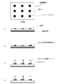
- FIG. 1 shows a plan view of a circuit board 1 with electrodes 2 .
- the circuit board used in the soldering method of the present invention is a circuit board provided with electrodes, and may be provided with one or more electrodes.
- a circuit board provided with a plurality of electrodes shown in FIG. chips, and wafers.
- a solder resist is formed on a part of the upper surface of the circuit board other than the electrodes.
- a circuit board provided with such electrodes for example, the above-described printed wiring board and the like can be given.
- the electrode surface is coated with UBM (Cu/Ni/Pd/Au, Cu/Ni/Au, Cu/Ni—P/Au, etc.). It is preferable to form an Under Bump Metallization layer or a Surface Finish treatment layer. In addition, if the electrode surface of the circuit board is contaminated with grease or other contaminants, the wettability with the solder is reduced, which adversely affects the bondability. is preferred. When degreasing, it is more preferable to apply ultrasonic waves because the cleaning effect is further enhanced. If the electrode surface does not have a UBM layer or a surface finish treatment layer, an oxide film is likely to be formed on the electrode surface.
- the liquid resin composition 3 for soldering of the present invention is applied, potted or printed on the electrodes 2 of the circuit board 1 having the electrodes 2 thereon. Even if the resin composition for soldering 3 of the present invention after application, potting or printing is liquid, it does not have fluidity such that it flows from the electrodes 2 to the extent that the electrodes 2 of the circuit board 1 are exposed. It has viscosity and fluidity to the extent that it stays on the electrode 2 so as not to expose the electrode 2 .
- soldered conductive pillars 4 are arranged substantially vertically on the electrodes 2 of the circuit board 1 covered with the soldering resin composition 3 of the present invention. At this time, the electrodes 2 of the circuit board 1 and the solder 4a portions of the soldered conductive pillars are arranged to face each other.
- a support carrier or the like can be used for arranging the conductive pillars 4 with solder.
- the circuit board 1 on which the soldered conductive pillars 4 are arranged is placed in an oven and heated at a predetermined temperature for a predetermined period of time to evaporate the solvent (C) contained in the solder bonding resin composition 3 of the present invention. , the resin composition 3 for soldering of the present invention is dried. As a result, the soldering resin composition 3 of the present invention is dried, and the soldered conductive pillars 4 arranged on the electrodes 2 of the circuit board 1 can be temporarily fixed to the circuit board 1 .
- the circuit board 1 to which the soldered conductive pillars 4 are temporarily fixed is passed through a reflow furnace to melt the solder 4a portions of the soldered conductive pillars, thereby performing reflow soldering.
- the resin composition for soldering 3 of the present invention becomes a cured thermosetting resin by reacting the thermoplastic resin (A) and the cross-linking agent (B) to form a three-dimensional cross-linked structure.
- the cured thermosetting resin having a three-dimensional crosslinked structure is shown in a rounded shape as shown in FIG. 1(d).
- FIG. 2 a soldering method and a circuit board manufacturing method in the case of double-sided bonding in which a reflow soldering process is performed after a molding process will be described.
- FIGS. 2A and 2B two circuit boards 1A and 1B having electrodes are prepared.
- the electrodes 2A and 2B on the circuit boards 1A and 1B are coated, potted or printed with the liquid resin compositions 3A and 3B for soldering of the present invention.
- soldered conductive pillars 4 are arranged substantially vertically on the electrodes 2A of the circuit board 1A covered with the soldering resin composition 3A of the present invention.
- the soldered conductive pillar has solders 4a and 4b on its upper and lower end faces, respectively.
- the electrodes 2A of the circuit board 1A and the soldered portions 4a of the soldered conductive pillars 4 are arranged to face each other.
- the circuit board 1A and the circuit board 1B on which the soldered conductive pillars 4 are arranged are combined so that the electrodes 2A and 2B face each other.
- the circuit boards 1A and 1B thus combined are placed in an oven and heated at a predetermined temperature for a predetermined period of time to evaporate the solvent (C) contained in the solder joint resin compositions 3A and 3B of the present invention.
- the soldering resin compositions 3A and 3B of the present invention are dried.
- the soldering resin compositions 3A and 3B of the present invention are dried, and the soldered conductive pillars 4 arranged on the circuit boards 1A and 1B can be temporarily fixed to the circuit boards 1A and 1B.
- the solvent (C) is dried at the same time for the circuit boards 1A and 1B to temporarily fix the soldered conductive pillars 4 is described, but it may be done separately.
- FIG. 2D after the state of FIG.
- the soldering resin composition 3A of the present invention is dried and solidified, and the soldered conductive pillar arranged on the circuit board 1A 4 is temporarily fixed to the circuit board 1A.
- the liquid soldering resin composition 3B of the present invention is applied, potted or printed on the electrodes 2B of the circuit board 1B in the same manner as in FIG. 2(b).
- soldered conductive pillar 4 temporarily fixed to the circuit board 1A is arranged so as to face the electrode 2B of the circuit board 1B, and the solder bonding resin composition 3B of the present invention is dried. After drying, the soldered conductive pillars 4 temporarily fixed to the circuit board 1A are temporarily fixed to the circuit board 1B.
- a molding material 5 is injected into the board group consisting of the combined circuit board 1A and circuit board 2B.
- a pre-curing step is performed in which the substrate group into which the molding material 5 is injected is passed through a reflow furnace or a curing furnace to temporarily harden the molding material 5 .
- the mold material 5 becomes a temporary hardened mold material.
- the pre-curing process is performed at a temperature lower than the reflow temperature in the reflow soldering process and slightly below the glass transition point of the mold material 5 .
- the time for the precuring step depends on the mold material 5 used, but is, for example, about 1 second to 30 minutes.
- the group of substrates on which the mold material 5 is temporarily hardened is passed through a reflow furnace to perform a reflow soldering process.
- the solder portions 4a and 4b of the soldered conductive pillar 4 are melted, thereby soldering the electrode 2A of the circuit board 1A and one end surface of the conductive pillar.
- the electrodes 2B of the circuit board 1B and the other end surfaces of the conductive pillars are soldered.
- the resin composition for soldering 3A and 3B of the present invention becomes a thermosetting resin cured product by reacting the thermoplastic resin (A) and the cross-linking agent (B) to form a three-dimensional cross-linked structure. .
- the injected mold material 5 is also cured by the reflow soldering process.
- FIG. 3 a soldering method and a circuit board manufacturing method in the case of double-sided bonding in which a molding process is performed after a reflow soldering process will be described.
- Two circuit boards 1A and 1B having electrodes 2A and 2B are prepared.
- the electrodes 2A and 2B on the circuit boards 1A and 1B are coated, potted or printed with the liquid resin compositions 3A and 3B for soldering of the present invention.
- the method of coating, potting or printing the liquid soldering resin composition 3A, 3B of the present invention on the electrodes 2A, 2B on the circuit boards 1A, 1B is shown in FIGS. 2(a) and 2(b). is similar to
- the soldered conductive pillars 4 are arranged substantially vertically on the electrodes 2A of the circuit board 1A covered with the soldering resin composition 3A of the present invention (see FIG. 2(c)).
- the soldered conductive pillar is provided with solder 4a, 4b on its upper and lower end faces, respectively.
- the electrodes 2A of the circuit board 1A and the soldered portions of the soldered conductive pillars 4 are arranged to face each other.
- the circuit board 1A and the circuit board 1B on which the soldered conductive pillars 4 are arranged are combined so that the electrodes 2A and 2B face each other.
- the circuit boards 1A and 1B thus combined are placed in an oven and heated at a predetermined temperature for a predetermined period of time to evaporate the solvent (C) contained in the solder joint resin compositions 3A and 3B of the present invention.
- the soldering resin compositions 3A and 3B of the present invention are dried.
- the soldering resin compositions 3A and 3B of the present invention are dried, and the soldered conductive pillars 4 arranged on the circuit boards 1A and 1B can be temporarily fixed to the circuit boards 1A and 1B.
- the solvent (C) is dried at the same time for the circuit boards 1A and 1B to temporarily fix the soldered conductive pillars 4 is described, but it may be done separately.
- FIG. 3(d) as shown in FIG. 2(c), after placing the soldered conductive pillars 4 on the circuit board 1A, the circuit board 1A with the soldered conductive pillars 4 placed thereon is placed in an oven. , by heating at a predetermined temperature and for a predetermined time to evaporate the solvent (C) contained in the soldering resin composition 3A of the present invention, the soldering resin composition 3A of the present invention is dried and solidified.
- soldered conductive pillars 4 arranged on the circuit board 1A to temporarily fix the soldered conductive pillars 4 arranged on the circuit board 1A to the circuit board 1A.
- the other solder of the soldered conductive pillar 4 temporarily fixed to the circuit board 1A is arranged so as to face the electrode 2B of the circuit board 1B, and the solder bonding resin composition 3B of the present invention is dried. After drying, the soldered conductive pillars 4 temporarily fixed to the circuit board 1A are temporarily fixed to the circuit board 1B.
- a board group consisting of the circuit board 1A and the circuit board 1B combined as described above is passed through a reflow furnace to perform a reflow soldering process.
- the solder portions 4a and 4b of the soldered conductive pillar 4 are melted, thereby soldering the electrode 2A of the circuit board 1A and one end surface of the conductive pillar.
- the electrodes 2B of the circuit board 1B and the other end surfaces of the conductive pillars are soldered.
- the resin composition for soldering 3A and 3B of the present invention becomes a thermosetting resin cured product by reacting the thermoplastic resin (A) and the cross-linking agent (B) to form a three-dimensional cross-linked structure. .
- the molding material 5 is injected into the substrate group that has undergone the reflow soldering process, and the molding process is performed to harden the molding material 5 .
- soldered conductive pillars having solders 4a and 4b on the upper and lower end surfaces of the conductive pillars were used for explanation.
- soldered conductive pillar a soldered conductive pillar having solder on only one end face can also be used.
- soldered conductive pillars having solder only on one end surface are used, the soldered conductive pillars are arranged on the circuit board 1A of the two circuit boards, and solder paste or the like is applied to the other circuit board 1B. Form a solder layer.
- solder bonding resin composition 3B of the present invention is not applied to the circuit board 1B on which the solder layer is formed with solder paste or the like. Therefore, the soldering resin composition 3a of the present invention effectively fixes circuit members such as soldered conductive pillars to a circuit board or the like until they are soldered in a reflow soldering process.
- FIG. 4(a) A method of soldering and a method of manufacturing a circuit board when using a conductive pillar block will be described with reference to FIG.
- two support carriers 6A and 6B are prepared.
- the liquid soldering resin composition 3A, 3B of the present invention is applied, potted or printed onto the support carrier. Even if the solder joint resin compositions 3A and 3B of the present invention after coating, potting or printing are liquid, they do not have such fluidity that the surfaces of the support carriers 6A and 6B are exposed. It has viscosity and fluidity to the extent that it stays.
- soldered conductive pillars 4 are arranged substantially vertically on the support carrier 6A covered with the solder joint resin composition 3A of the present invention. At this time, the soldered conductive pillar has solders 4a and 4b on its upper and lower end faces, respectively.
- the support carriers 6A and 6B thus combined are placed in an oven and heated at a predetermined temperature for a predetermined period of time to evaporate the solvent (C) contained in the solder joint resin compositions 3A and 3B of the present invention.
- the soldering resin compositions 3A and 3B of the present invention are dried.
- the soldering resin compositions 3A and 3B of the present invention are dried, and the soldered conductive pillars 4 arranged on the support carriers 6A and 6B can be temporarily fixed to the support carriers 6A and 6B.
- the solvent (C) is dried at the same time on the support carriers 6A and 6B to temporarily fix the soldered conductive pillars 4 is described, but it may be done separately.
- the circuit board 1A is replaced with the support carrier 6A, and the same state as in FIG.
- the soldering resin composition 3A of the present invention is dried and solidified.
- the soldered conductive pillars 4 arranged on the support carrier 6A are temporarily fixed to the support carrier 6A.
- the support carrier 6B is coated, potted or printed with the liquid resin composition 3B for soldering of the present invention in the same manner as in FIG. 2(b).
- the other solder of the soldered conductive pillar 4 temporarily fixed to the support carrier 6A is arranged so as to face the solder joint resin composition 3B of the present invention attached to the support carrier 6B,
- the soldering resin composition 3B is dried and solidified to temporarily fix the soldered conductive pillars 4 temporarily fixed to the support carrier 6A to the support carrier 6B.
- the molding material 5 is injected into the support carrier group consisting of the support carrier 6A and the support carrier 6B combined as described above.
- a pre-curing step is performed in which the support carrier group into which the molding material 5 is injected is passed through a reflow furnace or a curing furnace to temporarily harden the molding material 5 . As a result, the mold material 5 becomes a temporary hardened mold material.
- the pre-curing step is performed at a temperature slightly below the glass transition point of the mold material 5 .
- the time for the precuring step depends on the mold material 5 used, but is, for example, about 1 second to 30 minutes.
- the support carriers 6A and 6B are removed from the support carrier group that has undergone the precuring process, and the conductive pillar block made of the temporarily cured molding material containing the soldered conductive pillars 4 is separated.
- circuit boards 1A and 1B having electrodes 2A and 2B are placed on the upper and lower surfaces of the conductive pillar block, respectively, and passed through a reflow furnace to perform a reflow soldering process.
- the electrodes 2A and 2B are soldered to one end surface and the other end surface of the soldered conductive pillar 4 by melting the solder portion of the soldered conductive pillar 4, respectively.
- the resin composition for soldering 3A and 3B of the present invention becomes a thermosetting resin cured product by reacting the thermoplastic resin (A) and the cross-linking agent (B) to form a three-dimensional cross-linked structure.
- the temporary hardened mold material is also post-cured in the reflow soldering process to become a hardened mold material.
- the soldering is provided with solders 4a and 4b on the upper and lower end surfaces of the conductive pillars, respectively.
- the conductive pillar may be a soldered conductive pillar having solder only on one end face of the conductive pillar, or a conductive pillar having no solder on either of the upper or lower end faces of the conductive pillar. . In this case, it is sufficient that the electrodes of the circuit board facing the end faces of the conductive pillars not provided with solder are provided with solder.
- soldered conductive pillars having solder only on one end surface the soldered conductive pillars are arranged on the circuit board 1A of the two circuit boards, and solder paste or the like is applied to the other circuit board 1B. It is sufficient to form a solder layer by When conductive pillars having no solder on the upper and lower end surfaces are used, a solder layer of solder paste or the like may be formed on the circuit boards 1A and 1B.
- the resin composition for solder bonding of the present invention is used to temporarily fix solder on an electrode, but it can also be used to temporarily fix other circuit members. For example, it can be used for temporarily fixing conductive pillars and solder.
- a method of using the resin composition for soldering of the present invention an embodiment of applying it to an electrode has been described, but for example, it may be applied to circuit members such as solder, soldered conductive pillars, and conductive pillars.
- the circuit members are not limited to soldered conductive pillars, and may include semiconductor elements such as IC chips, connection parts such as solder paste and Cu pillars, resistors, and the like. Passive electrical components and the like are also applicable, and the circuit members may comprise, for example, solder bumps, Cu pillars, and the like.
- the present invention can also be applied to an IC chip or the like having a ball bump, in which the circuit member and the electrode do not have opposing surfaces, for example.
- solder joint resin composition of the present invention can be used for temporary fixing in the manufacturing process of electronic parts, and for masking in the film forming process such as painting, vapor deposition or sputtering, and can be used for paper, wood, glass, metal, semiconductor, It can be used as a temporary fixing member for workpieces such as ceramics, substrates, cloth, and plastics.
- Examples of electronic components include electronic components such as semiconductor elements, liquid crystal display elements, and solar cells.
- Manufacturing processes include, for example, the back grinding process of semiconductor wafers, the dicing process, the wire saw cutting process of silicon ingots, glass and ceramics. A cutting step and the like can be mentioned. By temporarily fixing works such as glass and ceramics with the resin composition for soldering of the present invention, laminating them, and then cutting them all at once, the productivity of cutting can be dramatically improved.
- Measurement method and evaluation method (1) Measurement method and evaluation method of die shear strength Each resin composition produced in Examples and Comparative Examples was applied to a copper substrate (FR-4) using an applicator with a thickness of 50 ⁇ m. was applied to prepare a substrate having a resin composition layer.
- the substrate FR-4 used is a glass epoxy substrate, the electrodes are made of copper, and the UBM layer on the electrode surface is Cu/Ni/Au (the thickness of the Ni layer is 3 ⁇ m and the thickness of the Au layer is 0.03 ⁇ m). ).
- the solder balls were placed on the coated resin composition layer on the copper substrate and dried at 120° C. for 30 minutes using an oven.
- die shear tester (Daisy Co. series 5000), a shear tool speed of 300 ⁇ m/s and a shear tool height of 30 ⁇ m from the material were applied to the solder balls on the substrate in parallel with the substrate. , the die shear strength was measured. Solder balls with a diameter of 0.76 mm and an alloy composition of SAC305 were used. The evaluation is as follows. ⁇ : Die shear strength is 700 g or more ⁇ : Die shear strength is 500 g or more and less than 700 ⁇ : Die shear strength is less than 500 g
- ⁇ Solder joint is performed, and the length of the joint between the solder ball and the substrate on the cut surface is 80% or more of the diameter of the solder ball.
- ⁇ Solder joint is performed, and the length of the joint between the solder ball and the substrate on the cut surface is 50% or more and less than 80% of the diameter of the solder ball.
- x Not soldered. Alternatively, the length of the joint between the solder ball and the substrate at the cut surface is less than 50% of the diameter of the solder ball.
- phenoxy resins, acid anhydrides and additives used in Examples and Comparative Examples are as follows. ⁇ Phenoxy resin> Phenoxy resin: YX7200B35 (manufactured by Mitsubishi Chemical Corporation, 2-butanone solution), solid content 35% by mass ⁇ Epoxy resin> Epoxy resin: jer828 (manufactured by Mitsubishi Chemical Corporation)
- TDA-100 Structure represented by formula (2) (Shin Nippon Rika Co., Ltd., Rikashid TDA-100)
- BT-100 Structure represented by formula (3) (Shin Nippon Rika Co., Ltd., Rikashid BT-100)
- BzDA structure represented by formula (4) (manufactured by ENEOS Corporation)
- BPDA structure represented by formula (5) (manufactured by JFE Chemical Co., Ltd.)
- Imidazole-based curing agent 2PHZPW (manufactured by Shikoku Kasei Kogyo Co., Ltd.)
- Example A After adding 257 parts by mass of diethylene glycol monomethyl ether to 286 parts by mass of 2-butanone solution of phenoxy resin (YX7200B35), 2-butanone was vacuum distilled to obtain 357 parts by mass of diethylene glycol solution of phenoxy resin. 50 parts by mass of TDA-100 was added to 357 parts by mass of a diethylene glycol solution of phenoxy resin and kneaded using a triple roll to obtain 407 parts by mass of a phenoxy resin composition.
- each phenoxy resin composition was obtained in the same manner except that the types or amounts of the solvent and cross-linking agent shown in Table 1 were used. rice field.
- Example E After adding 290 parts by mass of diethylene glycol monomethyl ether to 286 parts by mass of a phenoxy resin 2-butanone solution (YX7200B35), 2-butanone was vacuum distilled to obtain 390 parts by mass of a phenoxy resin diethylene glycol solution. 42 parts by mass of BPDA and 12 parts by mass of adipic acid were added to 290 parts by mass of a diethylene glycol solution of a phenoxy resin and kneaded using a triple roll to obtain 444 parts by mass of a phenoxy resin composition.
- Examples F and G Each phenoxy resin composition was obtained in the same manner, except that the types and amounts of the solvent and fluxing agent shown in Table 2 were used instead of 290 parts by mass of diethylene glycol monomethyl ether and 12 parts by mass of adipic acid in Example E. .
- Example H, I, N, O, P and Q Each phenoxy resin composition was prepared in the same manner, except that the types and amounts of the solvent, cross-linking agent and fluxing agent shown in Table 3 were used instead of 290 parts by mass of diethylene glycol monomethyl ether and 12 parts by mass of adipic acid in Example E. got
- Example J Each phenoxy resin composition was prepared in the same manner, except that the types or amounts of the solvent, cross-linking agent and fluxing agent shown in Table 4 were used instead of 290 parts by mass of diethylene glycol monomethyl ether and 12 parts by mass of adipic acid in Example E. got
- Examples R, M, K and L Each phenoxy resin composition was prepared in the same manner, except that the types or amounts of the solvent, cross-linking agent and fluxing agent listed in Table 5 were used instead of 290 parts by mass of diethylene glycol monomethyl ether and 12 parts by mass of adipic acid in Example E. got
- Example S A phenoxy resin was prepared in the same manner as in Example E, except that the types or amounts of the solvent, cross-linking agent, fluxing agent, and additives listed in Table 5 were used instead of 290 parts by mass of diethylene glycol monomethyl ether and 12 parts by mass of adipic acid in Example E. A composition was obtained.
- Comparative Example Using the components and amounts shown in Table 6, the resin composition of Comparative Example was obtained by manufacturing in the same manner as in Example A.
- the resin composition for soldering of the present invention has good fixing strength and good solderability.
- the resin composition for soldering of the present invention has a good fixing force, so that it is possible to fix electrical components without misalignment during soldering.
- solder joint resin composition of the present invention has good solder joint properties, so that solder joint defects can be suppressed when circuit boards are manufactured using a solder joint method or a solder joint method.
- soldering resin composition of the comparative example contains a large amount of epoxy resin that is liquid at room temperature as a thermoplastic resin compared to the soldering resin composition of the present invention in the example, the soldering resin composition after drying The composition cannot exert a temporary fixing force, the die shear strength is x, the solder jointability is also x, and it is not possible to fix the electrical parts in solder joints so that there is no misalignment, and it is also possible to suppress solder joint defects. I found out I can't.
- the solder bonding resin composition of the present invention can be used for temporary fixing in the manufacturing process of electronic components, and can be used for temporary fixing of processed materials such as paper, wood, glass, metals, semiconductors, ceramics, substrates, cloth, and plastics. It can be used as a fixing member.
Landscapes
- Engineering & Computer Science (AREA)
- Chemical & Material Sciences (AREA)
- Inorganic Chemistry (AREA)
- Mechanical Engineering (AREA)
- Manufacturing & Machinery (AREA)
- Microelectronics & Electronic Packaging (AREA)
- Adhesives Or Adhesive Processes (AREA)
- Compositions Of Macromolecular Compounds (AREA)
Priority Applications (1)
| Application Number | Priority Date | Filing Date | Title |
|---|---|---|---|
| JP2022576697A JPWO2022158460A1 (https=) | 2021-01-19 | 2022-01-18 |
Applications Claiming Priority (2)
| Application Number | Priority Date | Filing Date | Title |
|---|---|---|---|
| JP2021006771 | 2021-01-19 | ||
| JP2021-006771 | 2021-01-19 |
Publications (1)
| Publication Number | Publication Date |
|---|---|
| WO2022158460A1 true WO2022158460A1 (ja) | 2022-07-28 |
Family
ID=82549405
Family Applications (1)
| Application Number | Title | Priority Date | Filing Date |
|---|---|---|---|
| PCT/JP2022/001679 Ceased WO2022158460A1 (ja) | 2021-01-19 | 2022-01-18 | はんだ接合用樹脂組成物 |
Country Status (3)
| Country | Link |
|---|---|
| JP (1) | JPWO2022158460A1 (https=) |
| TW (1) | TW202245959A (https=) |
| WO (1) | WO2022158460A1 (https=) |
Citations (6)
| Publication number | Priority date | Publication date | Assignee | Title |
|---|---|---|---|---|
| JPH02104494A (ja) * | 1988-10-07 | 1990-04-17 | Hitachi Chem Co Ltd | プリント配線板の半田フラックス前駆体 |
| JP2003103398A (ja) * | 2001-09-26 | 2003-04-08 | Sumitomo Bakelite Co Ltd | 硬化性フラックスおよび硬化性フラックスシート |
| JP2010144150A (ja) * | 2008-12-22 | 2010-07-01 | Panasonic Electric Works Co Ltd | 熱硬化性樹脂組成物 |
| JP2013091093A (ja) * | 2011-10-27 | 2013-05-16 | Internatl Business Mach Corp <Ibm> | アンダーフィルとの間で化学的に硬化物を形成する無洗浄フラックス |
| WO2013125685A1 (ja) * | 2012-02-24 | 2013-08-29 | 日立化成株式会社 | 半導体装置及びその製造方法 |
| JP2013216830A (ja) * | 2012-04-11 | 2013-10-24 | Panasonic Corp | 熱硬化性樹脂組成物および半導体装置 |
-
2022
- 2022-01-18 WO PCT/JP2022/001679 patent/WO2022158460A1/ja not_active Ceased
- 2022-01-18 JP JP2022576697A patent/JPWO2022158460A1/ja active Pending
- 2022-01-19 TW TW111102165A patent/TW202245959A/zh unknown
Patent Citations (6)
| Publication number | Priority date | Publication date | Assignee | Title |
|---|---|---|---|---|
| JPH02104494A (ja) * | 1988-10-07 | 1990-04-17 | Hitachi Chem Co Ltd | プリント配線板の半田フラックス前駆体 |
| JP2003103398A (ja) * | 2001-09-26 | 2003-04-08 | Sumitomo Bakelite Co Ltd | 硬化性フラックスおよび硬化性フラックスシート |
| JP2010144150A (ja) * | 2008-12-22 | 2010-07-01 | Panasonic Electric Works Co Ltd | 熱硬化性樹脂組成物 |
| JP2013091093A (ja) * | 2011-10-27 | 2013-05-16 | Internatl Business Mach Corp <Ibm> | アンダーフィルとの間で化学的に硬化物を形成する無洗浄フラックス |
| WO2013125685A1 (ja) * | 2012-02-24 | 2013-08-29 | 日立化成株式会社 | 半導体装置及びその製造方法 |
| JP2013216830A (ja) * | 2012-04-11 | 2013-10-24 | Panasonic Corp | 熱硬化性樹脂組成物および半導体装置 |
Also Published As
| Publication number | Publication date |
|---|---|
| TW202245959A (zh) | 2022-12-01 |
| JPWO2022158460A1 (https=) | 2022-07-28 |
Similar Documents
| Publication | Publication Date | Title |
|---|---|---|
| EP1818351B1 (en) | Underfill encapsulant for wafer packaging and method for its application | |
| CN100342511C (zh) | 晶片组装使用的填充不足的密封剂及其应用方法 | |
| US7326369B2 (en) | Low stress conductive adhesive | |
| JP4537555B2 (ja) | 半導体パッケージの製造方法及び半導体パッケージ | |
| US11230649B2 (en) | Electrically conductive adhesive film and dicing-die bonding film using the same | |
| CN101002318A (zh) | 热塑性助熔底部填充组合物和方法 | |
| JP2005519169A (ja) | B−ステージに対応可能なアンダーフィル封入材料と、その利用方法 | |
| JP4684439B2 (ja) | 伝導性粒子、伝導性組成物および、電子機器の製造方法 | |
| JPWO2013125086A1 (ja) | 半導体用接着剤、フラックス剤、半導体装置の製造方法及び半導体装置 | |
| JP2005513779A (ja) | ウエハレベル用の二重硬化b−ステージ化可能なアンダーフィル | |
| JPWO2001047660A1 (ja) | 硬化性フラックス、半田接合用レジスト、該硬化性フラックスにより補強された半導体パッケージ及び半導体装置並びに該半導体パッケージ及び半導体装置の製造方法 | |
| WO2001047660A1 (en) | Hardening flux, soldering resist, semiconductor package reinforced by hardening flux, semiconductor device and method of producing semiconductor package and semiconductor device | |
| CN114664750B (zh) | 半导体封装体用底部填充膜及利用其的半导体封装体的制造方法 | |
| WO2022158460A1 (ja) | はんだ接合用樹脂組成物 | |
| TWI848023B (zh) | 補強用樹脂組成物、電子零件、電子零件之製造方法、安裝結構體及安裝結構體之製造方法 | |
| JP2001093940A (ja) | 半導体装置の組立方法 | |
| KR102696450B1 (ko) | 반도체 패키지용 언더필 필름 및 이를 이용하는 반도체 패키지의 제조방법 | |
| JP2022147854A (ja) | 仮固定組成物 | |
| JP4119356B2 (ja) | 半導体装置の製造方法及び半導体装置 | |
| JP4655501B2 (ja) | 液状封止樹脂組成物ならびに電子部品装置およびその製造方法 | |
| JP2022126264A (ja) | 樹脂組成物、硬化物、及び半導体装置 | |
| JP2004303874A (ja) | 半導体装置の製造方法及び半導体装置 | |
| JP2012216831A (ja) | 半導体チップ実装体の製造方法 | |
| JP5586313B2 (ja) | 接着剤層の形成方法、及び接着剤組成物 |
Legal Events
| Date | Code | Title | Description |
|---|---|---|---|
| 121 | Ep: the epo has been informed by wipo that ep was designated in this application |
Ref document number: 22742582 Country of ref document: EP Kind code of ref document: A1 |
|
| ENP | Entry into the national phase |
Ref document number: 2022576697 Country of ref document: JP Kind code of ref document: A |
|
| NENP | Non-entry into the national phase |
Ref country code: DE |
|
| 122 | Ep: pct application non-entry in european phase |
Ref document number: 22742582 Country of ref document: EP Kind code of ref document: A1 |