WO2022158053A1 - 半導体装置 - Google Patents
半導体装置 Download PDFInfo
- Publication number
- WO2022158053A1 WO2022158053A1 PCT/JP2021/036687 JP2021036687W WO2022158053A1 WO 2022158053 A1 WO2022158053 A1 WO 2022158053A1 JP 2021036687 W JP2021036687 W JP 2021036687W WO 2022158053 A1 WO2022158053 A1 WO 2022158053A1
- Authority
- WO
- WIPO (PCT)
- Prior art keywords
- side bottom
- region
- active
- bottom region
- outer peripheral
- Prior art date
Links
- 239000004065 semiconductor Substances 0.000 title claims abstract description 246
- 230000002093 peripheral effect Effects 0.000 claims abstract description 168
- 239000000758 substrate Substances 0.000 claims abstract description 108
- 239000012535 impurity Substances 0.000 claims description 37
- 238000010586 diagram Methods 0.000 description 38
- 239000000370 acceptor Substances 0.000 description 27
- 239000011229 interlayer Substances 0.000 description 25
- 239000000386 donor Substances 0.000 description 14
- 238000009825 accumulation Methods 0.000 description 13
- 238000000034 method Methods 0.000 description 13
- 125000004429 atom Chemical group 0.000 description 12
- 238000011084 recovery Methods 0.000 description 12
- 230000005684 electric field Effects 0.000 description 10
- 229910021420 polycrystalline silicon Inorganic materials 0.000 description 7
- 229920005591 polysilicon Polymers 0.000 description 7
- 229910052782 aluminium Inorganic materials 0.000 description 6
- XAGFODPZIPBFFR-UHFFFAOYSA-N aluminium Chemical compound [Al] XAGFODPZIPBFFR-UHFFFAOYSA-N 0.000 description 6
- 230000015556 catabolic process Effects 0.000 description 6
- 238000009826 distribution Methods 0.000 description 6
- 239000000126 substance Substances 0.000 description 6
- 230000000052 comparative effect Effects 0.000 description 5
- 229910052739 hydrogen Inorganic materials 0.000 description 5
- 239000001257 hydrogen Substances 0.000 description 5
- 150000002500 ions Chemical class 0.000 description 5
- 239000010410 layer Substances 0.000 description 5
- OAICVXFJPJFONN-UHFFFAOYSA-N Phosphorus Chemical compound [P] OAICVXFJPJFONN-UHFFFAOYSA-N 0.000 description 4
- XUIMIQQOPSSXEZ-UHFFFAOYSA-N Silicon Chemical compound [Si] XUIMIQQOPSSXEZ-UHFFFAOYSA-N 0.000 description 4
- 238000004519 manufacturing process Methods 0.000 description 4
- 239000000463 material Substances 0.000 description 4
- 229910052751 metal Inorganic materials 0.000 description 4
- 239000002184 metal Substances 0.000 description 4
- 229910052698 phosphorus Inorganic materials 0.000 description 4
- 239000011574 phosphorus Substances 0.000 description 4
- 229910052710 silicon Inorganic materials 0.000 description 4
- 239000010703 silicon Substances 0.000 description 4
- 230000007423 decrease Effects 0.000 description 3
- 230000007547 defect Effects 0.000 description 3
- 150000002431 hydrogen Chemical class 0.000 description 3
- 230000008569 process Effects 0.000 description 3
- ZOXJGFHDIHLPTG-UHFFFAOYSA-N Boron Chemical compound [B] ZOXJGFHDIHLPTG-UHFFFAOYSA-N 0.000 description 2
- 230000004888 barrier function Effects 0.000 description 2
- 229910052796 boron Inorganic materials 0.000 description 2
- 239000004020 conductor Substances 0.000 description 2
- 239000002019 doping agent Substances 0.000 description 2
- 230000000694 effects Effects 0.000 description 2
- 230000001747 exhibiting effect Effects 0.000 description 2
- 239000000852 hydrogen donor Substances 0.000 description 2
- 239000007769 metal material Substances 0.000 description 2
- 230000004048 modification Effects 0.000 description 2
- 238000012986 modification Methods 0.000 description 2
- 238000001004 secondary ion mass spectrometry Methods 0.000 description 2
- 230000007480 spreading Effects 0.000 description 2
- 238000003892 spreading Methods 0.000 description 2
- 229910000789 Aluminium-silicon alloy Inorganic materials 0.000 description 1
- UFHFLCQGNIYNRP-UHFFFAOYSA-N Hydrogen Chemical compound [H][H] UFHFLCQGNIYNRP-UHFFFAOYSA-N 0.000 description 1
- 229910000676 Si alloy Inorganic materials 0.000 description 1
- RTAQQCXQSZGOHL-UHFFFAOYSA-N Titanium Chemical compound [Ti] RTAQQCXQSZGOHL-UHFFFAOYSA-N 0.000 description 1
- KPSZQYZCNSCYGG-UHFFFAOYSA-N [B].[B] Chemical compound [B].[B] KPSZQYZCNSCYGG-UHFFFAOYSA-N 0.000 description 1
- 230000004913 activation Effects 0.000 description 1
- CSDREXVUYHZDNP-UHFFFAOYSA-N alumanylidynesilicon Chemical compound [Al].[Si] CSDREXVUYHZDNP-UHFFFAOYSA-N 0.000 description 1
- 229910052785 arsenic Inorganic materials 0.000 description 1
- RQNWIZPPADIBDY-UHFFFAOYSA-N arsenic atom Chemical compound [As] RQNWIZPPADIBDY-UHFFFAOYSA-N 0.000 description 1
- QVGXLLKOCUKJST-UHFFFAOYSA-N atomic oxygen Chemical compound [O] QVGXLLKOCUKJST-UHFFFAOYSA-N 0.000 description 1
- 239000000969 carrier Substances 0.000 description 1
- 239000013078 crystal Substances 0.000 description 1
- 238000009792 diffusion process Methods 0.000 description 1
- 230000005484 gravity Effects 0.000 description 1
- 230000012447 hatching Effects 0.000 description 1
- -1 hydrogen ions Chemical class 0.000 description 1
- 238000002347 injection Methods 0.000 description 1
- 239000007924 injection Substances 0.000 description 1
- 238000000691 measurement method Methods 0.000 description 1
- 229910001092 metal group alloy Inorganic materials 0.000 description 1
- 238000005121 nitriding Methods 0.000 description 1
- 230000001590 oxidative effect Effects 0.000 description 1
- 229910052760 oxygen Inorganic materials 0.000 description 1
- 239000001301 oxygen Substances 0.000 description 1
- 230000001737 promoting effect Effects 0.000 description 1
- 239000005368 silicate glass Substances 0.000 description 1
- 239000000243 solution Substances 0.000 description 1
- 238000003860 storage Methods 0.000 description 1
- 239000002344 surface layer Substances 0.000 description 1
- 239000010936 titanium Substances 0.000 description 1
- 229910052719 titanium Inorganic materials 0.000 description 1
- 150000003609 titanium compounds Chemical class 0.000 description 1
- WFKWXMTUELFFGS-UHFFFAOYSA-N tungsten Chemical compound [W] WFKWXMTUELFFGS-UHFFFAOYSA-N 0.000 description 1
- 229910052721 tungsten Inorganic materials 0.000 description 1
- 239000010937 tungsten Substances 0.000 description 1
Images


Classifications
-
- H—ELECTRICITY
- H01—ELECTRIC ELEMENTS
- H01L—SEMICONDUCTOR DEVICES NOT COVERED BY CLASS H10
- H01L29/00—Semiconductor devices adapted for rectifying, amplifying, oscillating or switching, or capacitors or resistors with at least one potential-jump barrier or surface barrier, e.g. PN junction depletion layer or carrier concentration layer; Details of semiconductor bodies or of electrodes thereof ; Multistep manufacturing processes therefor
- H01L29/02—Semiconductor bodies ; Multistep manufacturing processes therefor
- H01L29/06—Semiconductor bodies ; Multistep manufacturing processes therefor characterised by their shape; characterised by the shapes, relative sizes, or dispositions of the semiconductor regions ; characterised by the concentration or distribution of impurities within semiconductor regions
- H01L29/10—Semiconductor bodies ; Multistep manufacturing processes therefor characterised by their shape; characterised by the shapes, relative sizes, or dispositions of the semiconductor regions ; characterised by the concentration or distribution of impurities within semiconductor regions with semiconductor regions connected to an electrode not carrying current to be rectified, amplified or switched and such electrode being part of a semiconductor device which comprises three or more electrodes
- H01L29/1004—Base region of bipolar transistors
-
- H—ELECTRICITY
- H01—ELECTRIC ELEMENTS
- H01L—SEMICONDUCTOR DEVICES NOT COVERED BY CLASS H10
- H01L29/00—Semiconductor devices adapted for rectifying, amplifying, oscillating or switching, or capacitors or resistors with at least one potential-jump barrier or surface barrier, e.g. PN junction depletion layer or carrier concentration layer; Details of semiconductor bodies or of electrodes thereof ; Multistep manufacturing processes therefor
- H01L29/66—Types of semiconductor device ; Multistep manufacturing processes therefor
- H01L29/68—Types of semiconductor device ; Multistep manufacturing processes therefor controllable by only the electric current supplied, or only the electric potential applied, to an electrode which does not carry the current to be rectified, amplified or switched
- H01L29/70—Bipolar devices
- H01L29/72—Transistor-type devices, i.e. able to continuously respond to applied control signals
- H01L29/739—Transistor-type devices, i.e. able to continuously respond to applied control signals controlled by field-effect, e.g. bipolar static induction transistors [BSIT]
- H01L29/7393—Insulated gate bipolar mode transistors, i.e. IGBT; IGT; COMFET
- H01L29/7395—Vertical transistors, e.g. vertical IGBT
- H01L29/7396—Vertical transistors, e.g. vertical IGBT with a non planar surface, e.g. with a non planar gate or with a trench or recess or pillar in the surface of the emitter, base or collector region for improving current density or short circuiting the emitter and base regions
- H01L29/7397—Vertical transistors, e.g. vertical IGBT with a non planar surface, e.g. with a non planar gate or with a trench or recess or pillar in the surface of the emitter, base or collector region for improving current density or short circuiting the emitter and base regions and a gate structure lying on a slanted or vertical surface or formed in a groove, e.g. trench gate IGBT
-
- H—ELECTRICITY
- H01—ELECTRIC ELEMENTS
- H01L—SEMICONDUCTOR DEVICES NOT COVERED BY CLASS H10
- H01L29/00—Semiconductor devices adapted for rectifying, amplifying, oscillating or switching, or capacitors or resistors with at least one potential-jump barrier or surface barrier, e.g. PN junction depletion layer or carrier concentration layer; Details of semiconductor bodies or of electrodes thereof ; Multistep manufacturing processes therefor
- H01L29/02—Semiconductor bodies ; Multistep manufacturing processes therefor
- H01L29/06—Semiconductor bodies ; Multistep manufacturing processes therefor characterised by their shape; characterised by the shapes, relative sizes, or dispositions of the semiconductor regions ; characterised by the concentration or distribution of impurities within semiconductor regions
- H01L29/0603—Semiconductor bodies ; Multistep manufacturing processes therefor characterised by their shape; characterised by the shapes, relative sizes, or dispositions of the semiconductor regions ; characterised by the concentration or distribution of impurities within semiconductor regions characterised by particular constructional design considerations, e.g. for preventing surface leakage, for controlling electric field concentration or for internal isolations regions
- H01L29/0607—Semiconductor bodies ; Multistep manufacturing processes therefor characterised by their shape; characterised by the shapes, relative sizes, or dispositions of the semiconductor regions ; characterised by the concentration or distribution of impurities within semiconductor regions characterised by particular constructional design considerations, e.g. for preventing surface leakage, for controlling electric field concentration or for internal isolations regions for preventing surface leakage or controlling electric field concentration
- H01L29/0611—Semiconductor bodies ; Multistep manufacturing processes therefor characterised by their shape; characterised by the shapes, relative sizes, or dispositions of the semiconductor regions ; characterised by the concentration or distribution of impurities within semiconductor regions characterised by particular constructional design considerations, e.g. for preventing surface leakage, for controlling electric field concentration or for internal isolations regions for preventing surface leakage or controlling electric field concentration for increasing or controlling the breakdown voltage of reverse biased devices
- H01L29/0615—Semiconductor bodies ; Multistep manufacturing processes therefor characterised by their shape; characterised by the shapes, relative sizes, or dispositions of the semiconductor regions ; characterised by the concentration or distribution of impurities within semiconductor regions characterised by particular constructional design considerations, e.g. for preventing surface leakage, for controlling electric field concentration or for internal isolations regions for preventing surface leakage or controlling electric field concentration for increasing or controlling the breakdown voltage of reverse biased devices by the doping profile or the shape or the arrangement of the PN junction, or with supplementary regions, e.g. junction termination extension [JTE]
- H01L29/0619—Semiconductor bodies ; Multistep manufacturing processes therefor characterised by their shape; characterised by the shapes, relative sizes, or dispositions of the semiconductor regions ; characterised by the concentration or distribution of impurities within semiconductor regions characterised by particular constructional design considerations, e.g. for preventing surface leakage, for controlling electric field concentration or for internal isolations regions for preventing surface leakage or controlling electric field concentration for increasing or controlling the breakdown voltage of reverse biased devices by the doping profile or the shape or the arrangement of the PN junction, or with supplementary regions, e.g. junction termination extension [JTE] with a supplementary region doped oppositely to or in rectifying contact with the semiconductor containing or contacting region, e.g. guard rings with PN or Schottky junction
- H01L29/0623—Buried supplementary region, e.g. buried guard ring
-
- H—ELECTRICITY
- H01—ELECTRIC ELEMENTS
- H01L—SEMICONDUCTOR DEVICES NOT COVERED BY CLASS H10
- H01L29/00—Semiconductor devices adapted for rectifying, amplifying, oscillating or switching, or capacitors or resistors with at least one potential-jump barrier or surface barrier, e.g. PN junction depletion layer or carrier concentration layer; Details of semiconductor bodies or of electrodes thereof ; Multistep manufacturing processes therefor
- H01L29/02—Semiconductor bodies ; Multistep manufacturing processes therefor
- H01L29/06—Semiconductor bodies ; Multistep manufacturing processes therefor characterised by their shape; characterised by the shapes, relative sizes, or dispositions of the semiconductor regions ; characterised by the concentration or distribution of impurities within semiconductor regions
- H01L29/0684—Semiconductor bodies ; Multistep manufacturing processes therefor characterised by their shape; characterised by the shapes, relative sizes, or dispositions of the semiconductor regions ; characterised by the concentration or distribution of impurities within semiconductor regions characterised by the shape, relative sizes or dispositions of the semiconductor regions or junctions between the regions
- H01L29/0692—Surface layout
- H01L29/0696—Surface layout of cellular field-effect devices, e.g. multicellular DMOS transistors or IGBTs
-
- H—ELECTRICITY
- H01—ELECTRIC ELEMENTS
- H01L—SEMICONDUCTOR DEVICES NOT COVERED BY CLASS H10
- H01L29/00—Semiconductor devices adapted for rectifying, amplifying, oscillating or switching, or capacitors or resistors with at least one potential-jump barrier or surface barrier, e.g. PN junction depletion layer or carrier concentration layer; Details of semiconductor bodies or of electrodes thereof ; Multistep manufacturing processes therefor
- H01L29/40—Electrodes ; Multistep manufacturing processes therefor
- H01L29/402—Field plates
- H01L29/404—Multiple field plate structures
-
- H—ELECTRICITY
- H01—ELECTRIC ELEMENTS
- H01L—SEMICONDUCTOR DEVICES NOT COVERED BY CLASS H10
- H01L29/00—Semiconductor devices adapted for rectifying, amplifying, oscillating or switching, or capacitors or resistors with at least one potential-jump barrier or surface barrier, e.g. PN junction depletion layer or carrier concentration layer; Details of semiconductor bodies or of electrodes thereof ; Multistep manufacturing processes therefor
- H01L29/40—Electrodes ; Multistep manufacturing processes therefor
- H01L29/402—Field plates
- H01L29/407—Recessed field plates, e.g. trench field plates, buried field plates
-
- H—ELECTRICITY
- H01—ELECTRIC ELEMENTS
- H01L—SEMICONDUCTOR DEVICES NOT COVERED BY CLASS H10
- H01L29/00—Semiconductor devices adapted for rectifying, amplifying, oscillating or switching, or capacitors or resistors with at least one potential-jump barrier or surface barrier, e.g. PN junction depletion layer or carrier concentration layer; Details of semiconductor bodies or of electrodes thereof ; Multistep manufacturing processes therefor
- H01L29/40—Electrodes ; Multistep manufacturing processes therefor
- H01L29/41—Electrodes ; Multistep manufacturing processes therefor characterised by their shape, relative sizes or dispositions
- H01L29/423—Electrodes ; Multistep manufacturing processes therefor characterised by their shape, relative sizes or dispositions not carrying the current to be rectified, amplified or switched
- H01L29/42312—Gate electrodes for field effect devices
- H01L29/42316—Gate electrodes for field effect devices for field-effect transistors
- H01L29/4232—Gate electrodes for field effect devices for field-effect transistors with insulated gate
- H01L29/42372—Gate electrodes for field effect devices for field-effect transistors with insulated gate characterised by the conducting layer, e.g. the length, the sectional shape or the lay-out
- H01L29/4238—Gate electrodes for field effect devices for field-effect transistors with insulated gate characterised by the conducting layer, e.g. the length, the sectional shape or the lay-out characterised by the surface lay-out
-
- H—ELECTRICITY
- H01—ELECTRIC ELEMENTS
- H01L—SEMICONDUCTOR DEVICES NOT COVERED BY CLASS H10
- H01L29/00—Semiconductor devices adapted for rectifying, amplifying, oscillating or switching, or capacitors or resistors with at least one potential-jump barrier or surface barrier, e.g. PN junction depletion layer or carrier concentration layer; Details of semiconductor bodies or of electrodes thereof ; Multistep manufacturing processes therefor
- H01L29/02—Semiconductor bodies ; Multistep manufacturing processes therefor
- H01L29/06—Semiconductor bodies ; Multistep manufacturing processes therefor characterised by their shape; characterised by the shapes, relative sizes, or dispositions of the semiconductor regions ; characterised by the concentration or distribution of impurities within semiconductor regions
- H01L29/0603—Semiconductor bodies ; Multistep manufacturing processes therefor characterised by their shape; characterised by the shapes, relative sizes, or dispositions of the semiconductor regions ; characterised by the concentration or distribution of impurities within semiconductor regions characterised by particular constructional design considerations, e.g. for preventing surface leakage, for controlling electric field concentration or for internal isolations regions
- H01L29/0607—Semiconductor bodies ; Multistep manufacturing processes therefor characterised by their shape; characterised by the shapes, relative sizes, or dispositions of the semiconductor regions ; characterised by the concentration or distribution of impurities within semiconductor regions characterised by particular constructional design considerations, e.g. for preventing surface leakage, for controlling electric field concentration or for internal isolations regions for preventing surface leakage or controlling electric field concentration
- H01L29/0611—Semiconductor bodies ; Multistep manufacturing processes therefor characterised by their shape; characterised by the shapes, relative sizes, or dispositions of the semiconductor regions ; characterised by the concentration or distribution of impurities within semiconductor regions characterised by particular constructional design considerations, e.g. for preventing surface leakage, for controlling electric field concentration or for internal isolations regions for preventing surface leakage or controlling electric field concentration for increasing or controlling the breakdown voltage of reverse biased devices
- H01L29/0615—Semiconductor bodies ; Multistep manufacturing processes therefor characterised by their shape; characterised by the shapes, relative sizes, or dispositions of the semiconductor regions ; characterised by the concentration or distribution of impurities within semiconductor regions characterised by particular constructional design considerations, e.g. for preventing surface leakage, for controlling electric field concentration or for internal isolations regions for preventing surface leakage or controlling electric field concentration for increasing or controlling the breakdown voltage of reverse biased devices by the doping profile or the shape or the arrangement of the PN junction, or with supplementary regions, e.g. junction termination extension [JTE]
Definitions
- the present invention relates to semiconductor devices.
- Patent Document 1 JP-A-2019-91892
- Patent Document 2 JP-A-2019-110288
- a first aspect of the present invention provides a semiconductor device including a semiconductor substrate.
- the semiconductor substrate may have an active portion.
- the semiconductor substrate may have a peripheral well region of the second conductivity type.
- the outer well region may surround the active portion in top view.
- the semiconductor substrate may have a trench portion.
- the trench portion may be provided in the active portion on the upper surface of the semiconductor substrate.
- the active portion may have a central portion.
- the central portion may have an emitter region of the first conductivity type.
- the active portion may have a perimeter.
- the outer portion may surround the central portion.
- the central portion may have an active bottom region of the second conductivity type.
- the active side bottom region may span the bottom of at least two trench portions.
- the outer perimeter may have an outer perimeter bottom region of the second conductivity type.
- the outer bottom region may be electrically connected to the outer well region.
- the outer bottom region may be provided at the bottom of the trench toward the active bottom region.
- the active-side bottom region may also be provided in the outer peripheral portion.
- the active-side bottom region may be electrically floating.
- the trench part may be provided in a stripe shape when viewed from above.
- the outer peripheral bottom region may terminate at the bottom of the trench.
- the active side bottom region may terminate at the bottom of the trench.
- the impurity concentration of the active-side bottom region and the outer-peripheral-side bottom region may be the same.
- the impurity concentration of the outer peripheral side bottom region may be higher than the impurity concentration of the active side bottom region.
- the impurity concentration of the outer peripheral well region may be higher than the impurity concentration of the outer peripheral side bottom region.
- the active side bottom region and the outer peripheral side bottom region may be provided at the same depth in the depth direction of the semiconductor substrate.
- the outer peripheral side bottom region may be provided wider than the active side bottom region in the depth direction of the semiconductor substrate.
- the distance between the active-side bottom region and the outer-peripheral-side bottom region in the arrangement direction of the trench portions may be equal to or greater than the pitch width of the trench portions.
- the distance between the active-side bottom region and the outer peripheral-side bottom region in the arrangement direction of the trench portions may be 20 times or less the pitch width of the trench portions.
- the distance in the arrangement direction between the active-side bottom region and the outer peripheral-side bottom region may be 2 ⁇ m or more.
- the distance in the arrangement direction between the active-side bottom region and the outer peripheral-side bottom region may be 40 ⁇ m or less.
- the trench portion may have a gate trench portion.
- the trench portion may have a dummy trench portion.
- a gate trench portion may be provided between the active side bottom region and the outer peripheral side bottom region in the depth direction of the semiconductor substrate.
- the outer peripheral side bottom region may be provided in a range of five times or less the pitch width of the trench portions from the outer peripheral well region in the arrangement direction of the trench portions.
- the distance between the active-side bottom region and the outer peripheral-side bottom region in the arrangement direction of the trench portions may be larger than the width of the outer-peripheral-side bottom region.
- the trench portion has an outer peripheral deepened trench portion provided between the active side bottom region and the outer peripheral side bottom region in the arrangement direction of the trench portions in the outer peripheral portion and formed deeper than the active side bottom region and the outer peripheral side bottom region.
- the trench part may have an active-side deepened trench part at least partially provided in the central part and formed deeper than the active-side bottom region.
- the central portion may have a first-conductivity-type active-side bottom-less region sandwiched between the active-side bottom regions in a top view and provided at the same depth as the active-side bottom regions in the depth direction of the semiconductor substrate.
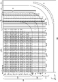
- FIG. 1 is a top view showing an example of a semiconductor device 100;
- FIG. 2 is an enlarged view of a region D in FIG. 1;
- FIG. FIG. 3 is a diagram showing an example of an ee cross section in FIG. 2;
- FIG. 3 is a diagram showing an example of the ff cross section in FIG. 2;
- FIG. 3 is a diagram showing an example of a gg cross section in FIG. 2;
- FIG. 3 is a diagram showing another example of the ee cross section in FIG. 2;
- It is a figure which shows an example of the semiconductor device 200 which concerns on a comparative example.
- FIG. 4 is a diagram showing the relationship between the forward current of the FWD and the slope of the reverse recovery voltage at room temperature;
- FIG. 4 is a diagram showing the relationship between the maximum value of the slope of the reverse recovery voltage of the FWD (at low current at room temperature) and the turn-on loss (at rated current at high temperature);
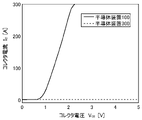
- 3 is a diagram showing IV characteristics of collector current and collector voltage when the gate voltage of the semiconductor devices 100 and 200 is 0 V (OFF);
- FIG. FIG. 4 is a diagram showing IV characteristics of collector currents and collector voltages of the semiconductor device 100 and the semiconductor device 300 when the gate voltage is 15 V (ON); It is a top view which shows an example of the semiconductor device 400 which concerns on other embodiment.
- FIG. 14 is a diagram showing an example of the hh cross section in FIG.
- FIG. 14 is a diagram showing an example of the ii section in FIG. 13;
- FIG. 14 is a diagram showing an example of a jj cross section in FIG. 13;
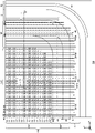
- It is a top view which shows an example of the semiconductor device 500 which concerns on other embodiment.
- It is a top view which shows an example of the semiconductor device 600 which concerns on other embodiment.
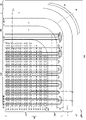
- FIG. 19 is a diagram showing an example of a kk cross section in FIG. 18; It is a top view which shows an example of the semiconductor device 700 which concerns on other embodiment.
- FIG. 21 is a diagram showing an example of an ll cross section in FIG. 20; It is a top view which shows an example of the semiconductor device 800 which concerns on other embodiment.
- FIG. 23 is a diagram showing an example of an mm section in FIG.
- FIG. 25 is a diagram showing an example of the nn cross section in FIG. 24;
- FIG. 25 is a diagram showing an example of an oo cross section in FIG. 24;
- FIG. 25 is a diagram showing an example of a pp cross section in FIG. 24;
- FIG. 25 is a diagram showing another example of the nn cross section in FIG. 24;
- one side in the direction parallel to the depth direction of the semiconductor substrate is called “upper”, and the other side is called “lower”.
- One of the two main surfaces of a substrate, layer or other member is called the upper surface and the other surface is called the lower surface.
- the directions of “up” and “down” are not limited to the direction of gravity or the direction when the semiconductor device is mounted.
- the Cartesian coordinate axes only specify the relative positions of the components and do not limit any particular orientation.
- the Z axis does not limit the height direction with respect to the ground.
- the +Z-axis direction and the ⁇ Z-axis direction are directions opposite to each other.
- the Z-axis direction is described without indicating positive or negative, it means a direction parallel to the +Z-axis and -Z-axis.
- orthogonal axes parallel to the upper and lower surfaces of the semiconductor substrate are defined as the X-axis and the Y-axis.
- the axis perpendicular to the upper and lower surfaces of the semiconductor substrate is defined as the Z-axis.
- the Z-axis direction may be referred to as the depth direction.
- a direction parallel to the upper and lower surfaces of the semiconductor substrate, including the X-axis and Y-axis may be referred to as a horizontal direction.
- the region from the center of the semiconductor substrate in the depth direction to the upper surface of the semiconductor substrate may be referred to as the upper surface side.
- the region from the center of the semiconductor substrate in the depth direction to the bottom surface of the semiconductor substrate may be referred to as the bottom surface side.
- the conductivity type of the doping region doped with impurities is described as P-type or N-type.
- impurities may specifically refer to either N-type donors or P-type acceptors, and may also be referred to as dopants.
- doping means introducing donors or acceptors into a semiconductor substrate to make it a semiconductor exhibiting N-type conductivity or a semiconductor exhibiting P-type conductivity.
- doping concentration means the concentration of donors or the concentration of acceptors at thermal equilibrium.
- the net doping concentration means the net concentration including the polarity of charges, where the donor concentration is the concentration of positive ions and the acceptor concentration is the concentration of negative ions.
- the donor concentration is N D and the acceptor concentration is N A
- the net net doping concentration at any location is N D ⁇ N A.
- net doping concentration may be simply referred to as doping concentration.
- a donor has the function of supplying electrons to a semiconductor.
- the acceptor has the function of receiving electrons from the semiconductor.
- Donors and acceptors are not limited to impurities per se.
- VOH defects in which vacancies (V), oxygen (O), and hydrogen (H) are combined in semiconductors function as donors that supply electrons.
- VOH defects are sometimes referred to herein as hydrogen donors.
- references herein to P+ type or N+ type refer to higher doping concentrations than P-type or N-type; references to P-type or N-type refer to higher doping than P-type or N-type. It means that the concentration is low.
- P++ type or N++ type in this specification means that the doping concentration is higher than that of the P+ type or N+ type.
- the unit system in this specification is the SI unit system unless otherwise specified. The unit of length is sometimes displayed in cm, but various calculations may be performed after converting to meters (m).
- chemical concentration refers to the atomic density of impurities measured regardless of the state of electrical activation.
- Chemical concentrations can be measured, for example, by secondary ion mass spectroscopy (SIMS).
- the net doping concentrations mentioned above can be measured by the voltage-capacitance method (CV method).
- the carrier concentration measured by the spreading resistance measurement method (SR method) may be used as the net doping concentration.
- the carrier concentration measured by the CV method or SR method may be a value in thermal equilibrium.
- the donor concentration is sufficiently higher than the acceptor concentration in the N-type region, the carrier concentration in the region may be used as the donor concentration.
- the carrier concentration in that region may be used as the acceptor concentration.
- the doping concentration of the N-type regions is sometimes referred to herein as the donor concentration
- the doping concentration of the P-type regions is sometimes referred to as the acceptor concentration.
- the peak value may be taken as the concentration of donors, acceptors or net doping in the region.
- the average concentration of donors, acceptors or net doping in the region may be used as the concentration of donors, acceptors or net doping.
- atoms/cm 3 or /cm 3 are used to express concentration per unit volume. This unit is used for donor or acceptor concentrations, or chemical concentrations, within a semiconductor substrate. The atoms notation may be omitted.
- the carrier concentration measured by the SR method may be lower than the donor or acceptor concentration.
- the carrier mobility of the semiconductor substrate may be lower than the value in the crystalline state. A decrease in carrier mobility is caused by scattering of carriers due to disorder of the crystal structure due to lattice defects or the like.
- the donor or acceptor concentration calculated from the carrier concentration measured by the CV method or the SR method may be lower than the chemical concentration of the element representing the donor or acceptor.
- the donor concentration of phosphorus or arsenic as a donor or the acceptor concentration of boron (boron) as an acceptor in a silicon semiconductor is about 99% of these chemical concentrations.
- the donor concentration of hydrogen serving as a donor in a silicon semiconductor is about 0.1% to 10% of the chemical concentration of hydrogen.
- Each concentration herein may be a value at room temperature. As an example of the value at room temperature, the value at 300 K (Kelvin) (approximately 26.9° C.) may be used.
- FIG. 1 is a top view showing an example of a semiconductor device 100.
- FIG. FIG. 1 shows the positions of each member projected onto the upper surface of the semiconductor substrate 10 .
- FIG. 1 only some members of the semiconductor device 100 are shown, and some members are omitted.
- a semiconductor device 100 includes a semiconductor substrate 10 .
- the semiconductor substrate 10 is a substrate made of a semiconductor material.
- the semiconductor substrate 10 is a silicon substrate, but the material of the semiconductor substrate 10 is not limited to silicon.
- the semiconductor substrate 10 has an edge 162 when viewed from above.
- simply referring to a top view means viewing from the top side of the semiconductor substrate 10 .
- the semiconductor substrate 10 of this example has two sets of edges 162 facing each other when viewed from above.
- the X-axis and Y-axis are parallel to one of the edges 162 .
- the Z-axis is perpendicular to the upper surface of the semiconductor substrate 10 .
- An active portion 160 is provided on the semiconductor substrate 10 .
- the active portion 160 is a region through which a main current flows in the depth direction between the upper and lower surfaces of the semiconductor substrate 10 when the semiconductor device 100 operates.
- An emitter electrode is provided above the active portion 160, but is omitted in FIG.
- the active section 160 is provided with a transistor section 70 including transistor elements such as IGBTs.
- transistor sections 70 and diode sections including diode elements such as FWD (Free Wheel Diode) may be alternately arranged along a predetermined arrangement direction on the upper surface of semiconductor substrate 10 .
- the transistor section 70 has a P+ type collector region in a region in contact with the lower surface of the semiconductor substrate 10 .
- a gate structure having an N++ type emitter region, a P ⁇ type base region, a gate conductive section and a gate insulating film is periodically arranged on the upper surface side of the semiconductor substrate 10.
- the semiconductor device 100 may have one or more pads above the semiconductor substrate 10 .
- the semiconductor device 100 of this example has a gate pad 164 .
- Semiconductor device 100 may have pads such as an anode pad, a cathode pad, and a current sensing pad. Each pad is arranged near the edge 162 .
- the vicinity of the edge 162 refers to a region between the edge 162 and the emitter electrode in top view.
- each pad may be connected to an external circuit via a wiring such as a wire.
- a gate potential is applied to the gate pad 164 .
- Gate pad 164 is electrically connected to the conductive portion of the gate trench portion of active portion 160 .
- the semiconductor device 100 includes a gate wiring 130 connecting the gate pad 164 and the gate trench portion. In FIG. 1, the gate wiring 130 is hatched with oblique lines.
- the gate wiring 130 is arranged between the active portion 160 and the edge 162 of the semiconductor substrate 10 when viewed from above.
- the gate wiring 130 of this example surrounds the active portion 160 when viewed from above.
- a region surrounded by the gate wiring 130 in top view may be the active portion 160 .
- the gate wiring 130 is connected to the gate pad 164 .
- the gate wiring 130 is arranged above the semiconductor substrate 10 .
- the gate wiring 130 may be a metal wiring containing aluminum or the like.
- the outer well region 11 is provided so as to overlap with the gate wiring 130 . In other words, like the gate wiring 130, the outer well region 11 surrounds the active portion 160 when viewed from above. The outer well region 11 is also provided to extend with a predetermined width in a range that does not overlap with the gate wiring 130 .
- the outer well region 11 is a region of the second conductivity type.
- the peripheral well region 11 in this example is of P+ type (see FIG. 2).
- the impurity concentration of outer well region 11 may be 5.0 ⁇ 10 17 atoms/cm 3 or more and 5.0 ⁇ 10 19 atoms/cm 3 or less.
- the impurity concentration of outer well region 11 may be 2.0 ⁇ 10 18 atoms/cm 3 or more and 2.0 ⁇ 10 19 atoms/cm 3 or less.
- the semiconductor device 100 also includes a temperature sensing portion (not shown), which is a PN junction diode made of polysilicon or the like, and a current detecting portion (not shown) that simulates the operation of the transistor portion 70 provided in the active portion 160.
- a temperature sensing portion (not shown), which is a PN junction diode made of polysilicon or the like, and a current detecting portion (not shown) that simulates the operation of the transistor portion 70 provided in the active portion 160.
- the semiconductor device 100 of this example includes an edge termination structure portion 90 between the active portion 160 and the edge 162 when viewed from above.
- the edge termination structure 90 in this example is located between the peripheral gate line 130 and the edge 162 .
- the edge termination structure 90 reduces electric field concentration on the upper surface side of the semiconductor substrate 10 .
- Edge termination structure 90 may include at least one of a guard ring, a field plate, and a resurf annularly surrounding active portion 160 .
- FIG. 2 is an enlarged view of area D in FIG.
- a region D is a region including the transistor section 70 .
- the semiconductor device 100 of this example includes a gate trench portion 40 , a dummy trench portion 30 , an outer peripheral well region 11 , an emitter region 12 and a contact region 15 provided inside the upper surface side of the semiconductor substrate 10 .
- Each of the gate trench portion 40 and the dummy trench portion 30 is an example of the trench portion.
- the semiconductor device 100 of this example includes emitter electrodes and gate wirings 130 provided above the upper surface of the semiconductor substrate 10 .
- the emitter electrode and gate line 130 are provided separately from each other.
- An interlayer insulating film is provided between the emitter electrode/gate wiring 130 and the upper surface of the semiconductor substrate 10 .
- the emitter electrode, gate wiring 130 and interlayer insulating film are omitted.
- the emitter electrode is provided above the gate trench portion 40 , the dummy trench portion 30 , the outer peripheral well region 11 , the emitter region 12 and the contact region 15 .
- the emitter electrode contacts emitter region 12 and contact region 15 on the upper surface of semiconductor substrate 10 through contact holes.
- the emitter electrode is connected to the dummy conductive portion in the dummy trench portion 30 through a contact hole provided in the interlayer insulating film.
- the emitter electrode may be connected to the dummy conductive portion of the dummy trench portion 30 at the tip portion 31 of the dummy trench portion 30 in the Y-axis direction.
- the gate wiring 130 is connected to the gate trench portion 40 through a contact hole provided in the interlayer insulating film.
- the gate wiring 130 may be connected to the gate conductive portion of the gate trench portion 40 at the tip portion 41 of the gate trench portion 40 in the Y-axis direction. Gate wiring 130 is not connected to the dummy conductive portion in dummy trench portion 30 .
- the emitter electrode is made of a material containing metal.
- at least a partial region of the emitter electrode is made of aluminum or a metal alloy such as an aluminum-silicon alloy such as AlSi, AlSiCu.
- the emitter electrode may have a barrier metal made of titanium, a titanium compound, or the like under the region made of aluminum or the like.
- the contact hole may have a plug formed by embedding tungsten or the like so as to be in contact with the barrier metal and the aluminum or the like.
- the transistor section 70 has a plurality of trench sections arranged in the arrangement direction.
- trench portions are provided in the active portion 160 and the outer well region 11 on the upper surface of the semiconductor substrate 10 .
- the trench portions are provided in a stripe shape in the top view of the transistor portion 70 .
- one or more gate trench sections 40 and one or more dummy trench sections 30 are alternately provided along the arrangement direction.
- one gate trench portion 40 and two dummy trench portions 30 are alternately provided.
- the gate trench portion 40 of this example connects the two straight portions 39 extending along the extending direction perpendicular to the arrangement direction (the portion of the trench that is linear along the extending direction) and the two straight portions 39 . It may have a tip 41 .
- the stretching direction in FIG. 2 is the Y-axis direction.
- At least a portion of the tip portion 41 is preferably provided in a curved shape when viewed from above.
- the dummy trench portions 30 are provided between the respective straight portions 39 of the gate trench portions 40 .
- One dummy trench portion 30 may be provided between the straight portions 39, or a plurality of dummy trench portions 30 may be provided.
- two dummy trench portions 30 are provided between each straight portion 39 .
- the dummy trench portion 30 may have a linear shape extending in the extending direction, and may have a linear portion 29 and a tip portion 31 like the gate trench portion 40 .
- each dummy trench portion 30 has a straight portion 29 and a tip portion 31 .
- the diffusion depth of the outer peripheral well region 11 may be deeper than the depths of the gate trench portion 40 and the dummy trench portion 30 .
- Y-axis direction ends of the gate trench portion 40 and the dummy trench portion 30 are provided in the outer peripheral well region 11 when viewed from above. That is, the bottom of each trench in the depth direction is covered with the outer well region 11 at the end of each trench in the Y-axis direction. As a result, electric field concentration at the bottom of each trench can be relaxed.
- the semiconductor device 100 may include the gate trench portion 40 or the dummy trench portion 30 that is entirely provided in the outer peripheral well region 11 when viewed from above.
- a mesa portion is provided between each trench portion in the arrangement direction.
- the mesa portion refers to a region sandwiched between trench portions inside the semiconductor substrate 10 .
- the upper end of the mesa portion is the upper surface of the semiconductor substrate 10 .
- the depth position of the lower end of the mesa portion is the same as the depth position of the lower end of the trench portion.
- the mesa portion of this example extends in the extension direction (Y-axis direction) along the trench on the upper surface of the semiconductor substrate 10 .
- the transistor section 70 is provided with the mesa section 60 .
- Each mesa portion 60 may be provided with at least one of the first conductivity type emitter region 12 and the second conductivity type contact region 15 .
- the emitter region 12 in this example is of N++ type and the contact region 15 is of P++ type.
- the emitter region 12 and the contact region 15 may be provided between the base region and the upper surface of the semiconductor substrate 10 in the depth direction.
- the mesa portion 60 of the transistor portion 70 has the emitter region 12 exposed on the upper surface of the semiconductor substrate 10 .
- the emitter region 12 is provided in contact with the gate trench portion 40 .
- the mesa portion 60 in contact with the gate trench portion 40 may be provided with the contact region 15 exposed to the upper surface of the semiconductor substrate 10 .
- the contact region 15 is exposed on the upper surface of the semiconductor substrate 10 in the mesa portion 60 and arranged closest to the gate wiring 130 .
- Each of the contact region 15 and the emitter region 12 in the mesa portion 60 is provided from one trench portion to the other trench portion in the X-axis direction.
- the contact regions 15 and the emitter regions 12 of the mesa portion 60 are alternately arranged along the extension direction (Y-axis direction) of the trench portion.
- the contact regions 15 and the emitter regions 12 of the mesa portion 60 may be provided in stripes along the extending direction (Y-axis direction) of the trench portion.
- an emitter region 12 is provided in a region in contact with the trench portion, and a contact region 15 is provided in a region sandwiched between the emitter regions 12 .
- the edge termination structure 90 is provided with a guard ring 92 .
- Edge termination structure 90 may be provided with a plurality of guard rings 92 .
- the impurity concentration of guard ring 92 may be the same as that of outer well region 11 .
- the active portion 160 has a central portion 170 and an outer peripheral portion 180 .
- Central portion 170 has emitter region 12 .
- Peripheral portion 180 surrounds central portion 170 .
- the outer peripheral portion 180 surrounds the central portion 170 in top view.
- the boundary between the central portion 170 and the outer peripheral portion 180 may be the emitter region 12 closest to the outer peripheral well region 11 in the X-axis direction or the Y-axis direction.
- a contact hole is provided above each mesa portion 60 of the central portion 170 .
- the contact hole in this example is provided above each region of the contact region 15 and the emitter region 12 .
- the contact hole may be arranged in the center of the mesa portion 60 in the arrangement direction (X-axis direction). In this example, contact holes are omitted.
- FIG. 2 shows an active-side bottom region 182 and an outer peripheral-side bottom region 184 provided in the semiconductor substrate 10 .
- An active bottom region 182 is provided in the central portion 170 .
- the outer peripheral side bottom region 184 is provided in the outer peripheral portion 180 . As shown in FIG. 2, the active side bottom region 182 and the perimeter side bottom region 184 are spaced apart.
- FIG. 3 is a diagram showing an example of the ee cross section in FIG.
- the ee section is the XZ plane passing through the emitter region 12 of the central portion 170 . Note that the dimensions in FIG. 3 do not necessarily match the dimensions in FIG.
- the semiconductor device 100 of this example has a semiconductor substrate 10, an interlayer insulating film 38, an emitter electrode 52, a collector electrode 24 and a gate wiring 130 in the cross section.
- the interlayer insulating film 38 is provided on the upper surface 21 of the semiconductor substrate 10 .
- the interlayer insulating film 38 is a film including at least one layer of an insulating film such as silicate glass doped with an impurity such as boron or phosphorus, a thermal oxide film, and other insulating films.
- the contact hole 54 described with reference to FIG. 2 is provided in the interlayer insulating film 38 .
- a contact hole 54 is partially provided above the outer well region 11 to connect the outer well region 11 to the emitter electrode.
- the emitter electrode 52 is provided above the interlayer insulating film 38 . Emitter electrode 52 is in contact with top surface 21 of semiconductor substrate 10 through contact hole 54 in interlayer insulating film 38 . Note that the emitter electrode 52 may be provided above the outer peripheral well region 11 . A gate wiring 130 may be provided above the outer well region 11 . A gate polysilicon 46 may be provided under the gate wiring 130 .
- the collector electrode 24 is provided on the bottom surface 23 of the semiconductor substrate 10 .
- Emitter electrode 52 and collector electrode 24 are made of a metal material such as aluminum.
- the direction (Z-axis direction) connecting the emitter electrode 52 and the collector electrode 24 is referred to as the depth direction.
- Each mesa portion 60 is provided with a base region 14 of the second conductivity type.
- Emitter region 12 and contact region 15 are provided between top surface 21 of semiconductor substrate 10 and base region 14 .
- the base region 14 in this example is P-type.
- the semiconductor substrate 10 has a first conductivity type drift region 18 .
- the drift region 18 in this example is N-type or N-type.
- the N++ type emitter region 12 and the P ⁇ type base region 14 are provided in order from the upper surface 21 side of the semiconductor substrate 10. As shown in FIG. A drift region 18 is provided below the base region 14 .
- the mesa portion 60 may be provided with an N+ type accumulation region 16 . Accumulation region 16 is disposed between base region 14 and drift region 18 .
- the emitter region 12 is exposed on the upper surface 21 of the semiconductor substrate 10 and provided in contact with the gate trench portion 40 .
- the emitter region 12 may be in contact with trench portions on both sides of the mesa portion 60 .
- Emitter region 12 has a higher doping concentration than drift region 18 .
- a base region 14 is provided below the emitter region 12 .
- the base region 14 in this example is provided in contact with the emitter region 12 .
- the base region 14 may contact trench portions on both sides of the mesa portion 60 .
- the impurity concentration peak of the base region 14 is, for example, 2.5 ⁇ 10 17 atoms/cm 3 .
- the impurity concentration of base region 14 may be 5.0 ⁇ 10 16 atoms/cm 3 or more and 1.0 ⁇ 10 18 atoms/cm 3 or less.
- the accumulation region 16 is provided below the base region 14 .
- the accumulation region 16 is an N+ type region with a higher doping concentration than the drift region 18 .
- Accumulation region 16 may have a concentration peak of donors, such as phosphorus or hydrogen donors.
- IE effect carrier injection promoting effect
- the accumulation region 16 may be provided so as to cover the entire bottom surface of the base region 14 in each mesa portion 60 .
- the P++ type contact region 15 and the P ⁇ type base region 14 are provided in order from the upper surface 21 side of the semiconductor substrate 10. As shown in FIG. A drift region 18 is provided below the base region 14 .
- the accumulation region 16 may be provided in the mesa portion 60 of the outer peripheral portion 180 .
- An N+ type buffer region 20 may be provided under the drift region 18 .
- the doping concentration of buffer region 20 is higher than the doping concentration of drift region 18 .
- Buffer region 20 may have a concentration peak with a higher doping concentration than drift region 18 .
- the doping concentration of the concentration peak refers to the doping concentration at the apex of the concentration peak.
- an average value of doping concentrations in a region where the doping concentration distribution is substantially flat may be used as the doping concentration of the drift region 18.
- the buffer region 20 may be formed by ion-implanting hydrogen (protons) or an N-type dopant such as phosphorus.
- the buffer region 20 of this example is formed by implanting hydrogen ions.
- the buffer region 20 may function as a field stop layer that prevents the depletion layer extending from the bottom end of the base region 14 from reaching the P+ type collector region 22 .
- a P+ type collector region 22 is provided under the buffer region 20 .
- the acceptor concentration of collector region 22 is higher than the acceptor concentration of base region 14 .
- Collector region 22 may contain the same acceptor as base region 14 or may contain a different acceptor.
- the acceptor of the collector region 22 is boron, for example. Elements that serve as acceptors are not limited to the above examples.
- the collector region 22 is exposed on the bottom surface 23 of the semiconductor substrate 10 and connected to the collector electrode 24 .
- Collector electrode 24 may contact the entire bottom surface 23 of semiconductor substrate 10 .
- Emitter electrode 52 and collector electrode 24 are made of a metal material such as aluminum.
- One or more gate trench portions 40 and one or more dummy trench portions 30 are provided on the upper surface 21 side of the semiconductor substrate 10 .
- Each trench extends from the upper surface 21 of the semiconductor substrate 10 through the base region 14 and reaches the drift region 18 .
- the contact region 15 and/or the accumulation region 16 are provided, each trench also passes through these doping regions and reaches the drift region 18.
- FIG. The fact that the trench penetrates the doping region is not limited to the order of forming the doping region and then forming the trench.
- a structure in which a doping region is formed between the trench portions after the trench portions are formed is also included in the structure in which the trench portion penetrates the doping regions.
- the gate trench portion 40 has a gate trench provided in the upper surface 21 of the semiconductor substrate 10, a gate insulating film 42 and a gate conductive portion 44.
- a gate insulating film 42 is provided to cover the inner wall of the gate trench.
- the gate insulating film 42 may be formed by oxidizing or nitriding the semiconductor on the inner wall of the gate trench.
- the gate conductive portion 44 is provided inside the gate insulating film 42 inside the gate trench. That is, the gate insulating film 42 insulates the gate conductive portion 44 and the semiconductor substrate 10 from each other.
- the gate conductive portion 44 is formed of a conductive material such as polysilicon.
- the gate conductive portion 44 may be provided longer than the base region 14 in the depth direction.
- the gate trench portion 40 in the cross section is covered with the interlayer insulating film 38 on the upper surface 21 of the semiconductor substrate 10 .
- the gate conductive portion 44 is electrically connected to the gate wiring 130 .
- a predetermined gate voltage is applied to the gate conductive portion 44 , a channel is formed by an electron inversion layer in the surface layer of the interface contacting the gate trench portion 40 in the base region 14 .
- the dummy trench portion 30 may have the same structure as the gate trench portion 40 in the cross section.
- the dummy trench section 30 has a dummy trench provided in the upper surface 21 of the semiconductor substrate 10 , a dummy insulating film 32 and a dummy conductive section 34 .
- the dummy conductive portion 34 is electrically connected to the emitter electrode 52 .
- a dummy insulating film 32 is provided to cover the inner wall of the dummy trench.
- the dummy conductive portion 34 is provided inside the dummy trench and inside the dummy insulating film 32 .
- the dummy insulating film 32 insulates the dummy conductive portion 34 from the semiconductor substrate 10 .
- the dummy conductive portion 34 may be made of the same material as the gate conductive portion 44 .
- the dummy conductive portion 34 is made of a conductive material such as polysilicon.
- the dummy conductive portion 34 may have the same length as the gate conductive portion 44 in the depth direction.
- the gate trench portion 40 and the dummy trench portion 30 of this example are covered with an interlayer insulating film 38 on the upper surface 21 of the semiconductor substrate 10 .
- the bottoms of the dummy trench portion 30 and the gate trench portion 40 may be curved (curved in cross section) convex downward.
- the semiconductor device 100 of this example is an IGBT, which is operated as a switching element in combination with a diode such as an FWD. Depending on the application, it is necessary to suppress the slope of the reverse recovery voltage of the FWD at low current and reduce noise.
- the semiconductor device 200 according to the comparative example when the external gate resistance connected to the gate conductive portion 44 is increased in order to suppress the slope of the reverse recovery voltage, the turn-on speed of the IGBT slows down at the rated current, and the turn-on loss decreases. Increase.
- the bottom region of the second conductivity type is provided at the bottom of the trench.
- the central portion 170 is provided with an active side bottom region 182 of the second conductivity type at the bottom of the trench portion.
- Active side bottom region 182 in this example is P-type.
- An active side bottom region 182 covers the bottom of the trench.
- An active side bottom region 182 spans the bottom of at least two trench portions.
- An active side bottom region 182 may be provided below the base region 14 .
- the provision of the second conductivity type active-side bottom region 182 makes it easier to control the slope of the reverse recovery voltage of the FWD. Therefore, turn-on loss can be reduced. Also, the breakdown voltage can be improved by providing the active-side bottom region 182 .
- the outer peripheral portion 180 is provided with an outer peripheral side bottom region 184 of the second conductivity type at the bottom of the trench portion.
- the outer bottom region 184 in this example is P-type.
- the outer bottom region 184 covers the bottom of the trench.
- the outer bottom region 184 may be provided toward the active bottom region 182 . That is, the outer peripheral side bottom region 184 may be provided at the same depth as the active side bottom region 182 in the depth direction of the semiconductor substrate 10 .
- the outer peripheral side bottom region 184 is electrically connected to the outer peripheral well region 11 . In this example, the outer bottom region 184 is directly connected to the outer well region 11 . Therefore, the electric field concentration at the boundary between the outer peripheral well region 11 and the outer peripheral side bottom region 184 can be alleviated, and the avalanche resistance at the time of turn-off can be improved.
- the active side bottom region 182 and the outer peripheral side bottom region 184 are provided apart. That is, at least part of the outer peripheral portion 180 is not provided with a bottom region. Since the active-side bottom region 182 and the outer peripheral-side bottom region 184 are provided apart from each other, it is possible to prevent the active-side bottom region 182 and the outer peripheral well region 11 from having the same potential. Therefore, it is possible to prevent the semiconductor device 100 from failing to operate.
- Active side bottom region 182 may be electrically floating. Active-side bottom region 182 is said to be electrically floating if it is not electrically connected to any electrode. Also, the active-side bottom region 182 may not be partially provided in the active portion 160 . That is, the active-side bottom region 182 does not have to be provided over the entire active portion 160 .
- the active-side bottom region 182 may also be provided in the outer peripheral portion 180 . That is, the active-side bottom region 182 is provided wider than the range in which the emitter regions 12 are provided in the arrangement direction of the trench portions.
- the active-side bottom region 182 may be provided on at least a portion of the outer peripheral portion 180 .
- the concentration of the base region 14 changes, and the threshold value of the semiconductor device 100 fluctuates. Therefore, by providing the emitter region 12 only at the portion where the concentration of the base region 14 is changed, the fluctuation of the threshold value can be suppressed. If the active-side bottom region 182 is provided over the entire outer peripheral portion 180 , the active-side bottom region 182 will be connected to the outer peripheral well region 11 . Therefore, it is preferable that the active-side bottom region 182 is not provided in at least a portion of the outer peripheral portion 180 .
- the bottom region may terminate at the bottom of the trench. That is, the bottom region does not terminate at mesa 60 .
- the active side bottom region 182 terminates at the bottom of the trench.
- the outer peripheral bottom region 184 terminates at the bottom of the trench.
- the impurity concentration of the active-side bottom region 182 and the outer-peripheral-side bottom region 184 may be the same. By making the impurity concentration of the active-side bottom region 182 and the outer-peripheral-side bottom region 184 the same, the manufacturing process can be made the same. Also, the impurity concentration of the outer peripheral side bottom region 184 may be higher than the impurity concentration of the active side bottom region 182 . By making the impurity concentration of the outer peripheral side bottom region 184 higher than the impurity concentration of the active side bottom region 182, the effect of alleviating local electric field concentration is enhanced. The impurity concentration of the outer peripheral well region 11 may be higher than the impurity concentration of the outer peripheral side bottom region 184 .
- the impurity concentration peak of each bottom region is, for example, 4.0 ⁇ 10 15 atoms/cm 3 .
- the impurity concentration peak of each bottom region may be 3.0 ⁇ 10 14 atoms/cm 3 or more and 3.0 ⁇ 10 16 atoms/cm 3 or less.
- the dose of ions implanted into each bottom region may be 1.0 ⁇ 10 11 ion/cm 2 or more and 1.0 ⁇ 10 13 ion/cm 2 or less.
- the distance L between the active-side bottom region 182 and the outer-peripheral-side bottom region 184 in the arrangement direction of the trench portions may be equal to or greater than the pitch width W1 of the trench portions.
- the pitch width W1 of the trench portion is the distance from the center of the conductive portion of the trench portion to the center of the conductive portion of the adjacent trench portion.
- a distance L between the active-side bottom region 182 and the outer-peripheral-side bottom region 184 in the arrangement direction of the trench portions may preferably be twice or more the pitch width W1 of the trench portions.
- a distance L between the active-side bottom region 182 and the outer-peripheral-side bottom region 184 in the arrangement direction of the trench portions may be 20 times or less the pitch width W1 of the trench portions. By doing so, the range in which the active-side bottom region 182 is provided can be widened.
- a distance L between the active-side bottom region 182 and the outer-peripheral-side bottom region 184 in the arrangement direction of the trench portions may preferably be six times or less the pitch width W1 of the trench portions.
- the distance L between the active-side bottom region 182 and the outer-peripheral-side bottom region 184 in the arrangement direction of the trench portions is five times the pitch width W1 of the trench portions. Also, the distance L may be 10 to 15 times the pitch width W1 of the trench portion.
- the distance L in the arrangement direction between the active-side bottom region 182 and the outer peripheral-side bottom region 184 may be 2 ⁇ m or more.
- a distance L in the arrangement direction between the active-side bottom region 182 and the outer peripheral-side bottom region 184 may preferably be 4 ⁇ m or more.
- a distance L in the arrangement direction between the active-side bottom region 182 and the outer peripheral-side bottom region 184 may be 40 ⁇ m or less.
- a distance L in the arrangement direction between the active-side bottom region 182 and the outer peripheral-side bottom region 184 may preferably be 12 ⁇ m or less.
- a distance L in the arrangement direction between the active-side bottom region 182 and the outer peripheral-side bottom region 184 is, for example, 10 ⁇ m. Also, the distance L may be 30 ⁇ m or more and 35 ⁇ m or less.
- the outer peripheral side bottom region 184 may be provided in a range from the outer peripheral well region 11 to five times or less the pitch width W1 of the trench portions in the arrangement direction of the trench portions.
- the outer peripheral side bottom region 184 is provided in a range of three times or less the pitch width W1 of the trench portions from the outer peripheral well region 11 in the arrangement direction of the trench portions.
- the active-side bottom region 182 and the outer peripheral-side bottom region 184 can be sufficiently separated, and the semiconductor device 100 can be prevented from not operating.
- the distance L in the arrangement direction between the active-side bottom region 182 and the outer peripheral-side bottom region 184 may be larger than the width W2 in which the outer peripheral-side bottom region 184 is provided.
- the width W2 of the outer peripheral side bottom region 184 is, for example, 7 ⁇ m.
- a gate trench portion 40 is preferably provided between the active side bottom region 182 and the outer peripheral side bottom region 184 in the depth direction of the semiconductor substrate 10 .
- the presence of the gate trench portion 40 between the active-side bottom region 182 and the outer peripheral-side bottom region 184 in the depth direction of the semiconductor substrate 10 can suppress the influence of the ground potential.
- the distance L in the arrangement direction of the trench portions between the active-side bottom region 182 and the outer peripheral-side bottom region 184 is equal to the gate trench portion.
- the ratio of 40 to the dummy trench portion 30 is 1:2, it may be three times or more the pitch width W1 of the trench portions. Further, in this case, when the ratio of the gate trench portion 40 and the dummy trench portion 30 is 1:X, the distance L may be 1+X times or more.
- the distance L in the arrangement direction of the trench portions should be equal to or greater than the pitch width W1 of the trench portions.
- the distance L in the arrangement direction of the trench portions between the active-side bottom region 182 and the outer peripheral-side bottom region 184 is equal to the gate trench portion.
- the ratio of 40 to dummy trench portion 30 is 1:2, it is sufficient that the pitch width W1 of the trench portion is at least twice. In this case, when the ratio of the gate trench portion 40 to the dummy trench portion 30 is 1:X, the distance L may be X times or more.
- the accumulation region 16 is preferably provided wider than the active-side bottom region 182 .
- the accumulation region 16 is provided wider than the active-side bottom region 182 in the X-axis direction. With such a configuration, the accumulation region 16 and the active-side bottom region 182 can be easily formed.
- the storage region 16 does not overlap the bottom region 184 on the outer peripheral side in the depth direction.
- FIG. 4 is a diagram showing an example of the ff section in FIG.
- the ff cross section is the YZ plane passing through the tip portion 41 of the gate trench portion 40 and the tip portion 31 of the dummy trench portion 30 . Note that the dimensions in FIG. 4 do not necessarily match the dimensions in FIG.
- the semiconductor device 100 of this example has a semiconductor substrate 10, an interlayer insulating film 38, an emitter electrode 52, a collector electrode 24 and a gate wiring 130 in the cross section.
- the gate trench portion 40 is connected to the gate wiring 130 .
- the dummy trench portion 30 is connected to the emitter electrode 52 through the contact hole 56 .
- a dummy polysilicon 36 may be provided under the emitter electrode 52 .
- the outer peripheral side bottom region 184 may be provided at the same depth as the active side bottom region 182 in the depth direction of the semiconductor substrate 10, as in FIG.
- FIG. 5 is a diagram showing an example of a gg section in FIG.
- the gg section is the YZ plane passing through the straight portion 29 of the dummy trench portion 30 .
- the semiconductor device 100 of this example has a semiconductor substrate 10, an interlayer insulating film 38, an emitter electrode 52, a collector electrode 24 and a gate wiring 130 in the cross section.
- an interlayer insulating film 38 is provided between the emitter electrode 52 and the dummy trench portion 30 .
- the outer peripheral side bottom region 184 may be provided at the same depth as the active side bottom region 182 in the depth direction of the semiconductor substrate 10 .
- FIG. 6 is a diagram showing another example of the ee cross section in FIG. FIG. 6 is different from FIG. 2 in that the outer peripheral side bottom region 184 is provided wider than the active side bottom region 182 in the depth direction of the semiconductor substrate 10 . Otherwise, the configuration of FIG. 6 may be the same as that of FIG. In this example, the outer bottom region 184 is wider on the lower surface 23 side than the active bottom region 182 and has substantially the same depth as the outer well region 11 . Since the outer peripheral side bottom region 184 is wider than the active side bottom region 182, the electric field distribution can be adjusted.
- FIG. 7 is a diagram showing an example of a semiconductor device 200 according to a comparative example.
- FIG. 7 differs from FIG. 3 in that the active side bottom region 182 and the outer peripheral side bottom region 184 are not provided.
- Other configurations in FIG. 7 may be the same as in FIG.
- FIG. 8 is a diagram showing an example of a semiconductor device 300 according to a comparative example.
- FIG. 8 differs from FIG. 3 in that the active side bottom region 182 and the outer peripheral side bottom region 184 are connected.
- Other configurations in FIG. 8 may be the same as in FIG.
- the boundary between the active side bottom region 182 and the outer peripheral side bottom region 184 may be the boundary between the central portion 170 and the outer peripheral portion 180 .
- FIG. 9 is a diagram showing the relationship between the forward current of the FWD and the slope of the reverse recovery voltage at room temperature.
- the forward current is shown as a ratio when the rated current is 1.
- the external gate resistance is adjusted so that the slope of the reverse recovery voltage is the same (approximately 5 kV/ ⁇ sec) when the forward current is 5 to 10% (low current). is doing.
- the semiconductor device 100 can keep the slope of the reverse recovery voltage of the FWD at the same level as the semiconductor device 200 even if the forward current is changed. Therefore, when the forward current is 100% (at the rated current), the turn-on speed of the IGBT side does not slow down, and it can be kept as fast as when the forward current is 5 to 10% (at the low current). , turn-on losses can be reduced.
- FIG. 10 is a diagram showing the relationship between the maximum value of the slope of the reverse recovery voltage of the FWD (at low current at room temperature) and the turn-on loss (at rated current at high temperature).
- FIG. 10 can be obtained by plotting the maximum value of the slope of the reverse recovery voltage on the FWD side and the turn-on loss on the IGBT side on a one-to-one basis while changing the external gate resistance. From FIG. 10, when comparing the semiconductor device 100 and the semiconductor device 200 with the maximum value of the slope of the reverse recovery voltage of the FWD being 5 kV/ ⁇ sec, the turn-on loss can be reduced by approximately 50%.
- FIG. 11 is a diagram showing the IV characteristics of the collector current and the collector voltage when the gate voltage of the semiconductor device 100 and the semiconductor device 200 is 0 V (OFF).
- the collector voltage is shown as a ratio when the semiconductor device 200 is set to 1.
- FIG. 12 is a diagram showing IV characteristics of the collector current and the collector voltage when the gate voltage of the semiconductor devices 100 and 300 is 15 V (ON). As shown in FIG. 12, the semiconductor device 300 does not operate when the active side bottom region 182 and the outer peripheral side bottom region 184 are connected.
- FIG. 13 is a top view showing an example of a semiconductor device 400 according to another embodiment.
- the semiconductor device 400 of FIG. 13 differs from the semiconductor device 100 of FIG. 2 in the arrangement of the bottom region 190 . 13 differs from the semiconductor device 100 of FIG. 2 in that an outer peripheral deep trench portion 140 is provided.
- Other configurations of the semiconductor device 400 of FIG. 13 may be the same as those of the semiconductor device 100 of FIG.
- FIG. 13 shows a bottom region 190 provided within the semiconductor substrate 10 .
- the bottom region 190 has an active bottom region 182 (not shown in FIG. 13), an outer peripheral bottom region 184 (not shown in FIG. 13), and an outer intermediate bottom region which will be described later.
- the bottom region 190 does not have to be partially provided in the active portion 160 .
- the bottom region 190 is not partially provided on the perimeter 180 .
- a region where the bottom region 190 is not provided is a bottom-less region 192 .
- the bottomless region 192 is provided at the same depth as the bottom region 190 in the depth direction of the semiconductor substrate 10 .
- a first conductivity type drift region 18 is provided in the bottomless region 192 .
- the bottomless region 192 is provided so as to be in contact with the outer peripheral side deepened trench portion 140 provided closest to the central portion 170 in the arrangement direction (X-axis direction) of the trench portions.
- the bottomless region 192 By arranging the bottomless region 192 in this way, the bottom region 190 (active side bottom region 182) provided in the central portion 170 and the bottom portion provided in the outer peripheral portion 180 in the extending direction (Y-axis direction) of the trench portion It is possible to prevent the region 190 (outer peripheral side bottom region 184) from being connected. Note that the bottomless region 192 may partially overlap the outer peripheral side deepened trench portion 140 .
- the transistor section 70 has a plurality of deepened trench sections arranged in the arrangement direction.
- the trench portion has a deepened trench portion.
- the deepened trench portion is provided in the active portion 160 on the top surface of the semiconductor substrate 10 .
- the deepened trench portion is provided in the outer peripheral portion 180 .
- the deepened trench portion provided in the outer peripheral portion 180 is referred to as the outer peripheral side deepened trench portion 140 .
- the outer peripheral side deepened trench portion 140 may be provided in the outer peripheral well region 11 .
- the outer deep trench portion 140 may not be provided in the central portion 170 .
- the outer peripheral side deepened trench portion 140 is indicated by hatching.
- the outer peripheral side deepened trench portion 140 has a trench provided on the upper surface 21 of the semiconductor substrate 10, an insulating film, and a conductive portion.
- the outer peripheral deepened trench portion 140 may function as a dummy trench portion.
- a conductive portion of the outer peripheral deepened trench portion 140 may be connected to the emitter electrode 52 .
- the outer peripheral deepened trench portion 140 may function as a gate trench portion.
- a conductive portion of the outer deep trench portion 140 may be connected to the gate wiring 130 .
- the outer peripheral deepened trench portion 140 may have two straight portions 49 extending along the extending direction perpendicular to the arrangement direction (trench portions that are linear along the extending direction).
- the outer deep trench portion 140 may have a tip portion 51 connecting the two straight portions 49 .
- At least a part of the tip portion 51 is preferably provided in a curved shape when viewed from above.
- FIG. 14 is a diagram showing an example of the hh cross section in FIG.
- the hh section is the XZ plane passing through the emitter region 12 of the central portion 170 . Note that the dimensions in FIG. 14 do not necessarily match the dimensions in FIG.
- the semiconductor device 400 of this example has the semiconductor substrate 10, the interlayer insulating film 38, the emitter electrode 52, the collector electrode 24, and the gate wiring 130 in the cross section.
- the outer peripheral side deepened trench portion 140 is formed deeper than the bottom region 190 .
- the outer peripheral deepened trench portion 140 may be formed deeper than the gate trench portion 40 .
- the outer peripheral deepened trench portion 140 may be formed deeper than the dummy trench portion 30 .
- the outer peripheral deepened trench portion 140 may be formed deeper than the outer peripheral well region 11 .
- the bottom region 190 can be divided.
- the bottom region 190 provided closer to the central portion 170 than the outer deep trench portion 140 in the arrangement direction of the trench portions is referred to as an active-side bottom region 182 .
- the bottom region 190 provided between the outer deepened trench portions 140 in the arrangement direction of the trench portions is referred to as the outer intermediate bottom region 186 .
- the bottom region 190 provided between the outer deep trench portion 140 and the outer well region 11 in the arrangement direction of the trench portions is referred to as the outer bottom region 184 .
- the outer deep trench portion 140 is provided in the outer peripheral portion 180 between the active side bottom region 182 and the outer peripheral side bottom region 184 in the arrangement direction of the trench portions. Further, the outer peripheral side deepened trench portion 140 is formed deeper than the active side bottom region 182 . The outer deep trench portion 140 is formed deeper than the outer bottom region 184 .
- the active side bottom region 182 can be separated from the outer peripheral side bottom region 184 and the outer peripheral side intermediate bottom region 186, and the active side bottom region 182 can be electrically floating. Therefore, it is possible to improve the controllability of the slope of the reverse recovery voltage. Further, by providing the outer peripheral side bottom region 184 and the outer peripheral side intermediate bottom region 186, the breakdown voltage imbalance of the semiconductor device 400 can be eliminated.
- the impurity concentration of the active-side bottom region 182, the outer-peripheral-side bottom region 184, and the outer-peripheral-side intermediate bottom region 186 may be the same.
- the manufacturing process can be made the same.
- the impurity concentrations of the active-side bottom region 182, the outer-peripheral-side bottom region 184, and the outer-peripheral-side intermediate bottom region 186 may be different. Further, the impurity concentration of the active-side bottom region 182 and the outer peripheral-side bottom region 184 may be the same, and only the impurity concentration of the outer-peripheral-side intermediate bottom region 186 may be different.
- the width W3 of the outer peripheral deepened trench portion 140 in the arrangement direction of the trench portions may be 5.0 ⁇ m or more.
- a width W3 in which the outer peripheral side deepened trench portions 140 are provided in the arrangement direction of the trench portions may be equal to or greater than the pitch width W1 of the trench portions other than the outer peripheral side deepened trench portions 140 .
- the pitch width W1 of the trench portions other than the outer peripheral deepened trench portion 140 may be the same as the pitch width W1 of the trench portions in FIG.
- a width W3 in which the outer peripheral side deepened trench portions 140 are provided in the arrangement direction of the trench portions may be twice or more the pitch width W1 of the trench portions other than the outer peripheral side deepened trench portions 140 .
- the pitch width W4 of the outer peripheral side deepened trench portion 140 may be the same as the pitch width W1 of the trench portions other than the outer peripheral side deepened trench portion 140 .
- the pitch width W4 of the outer peripheral side deepened trench portions 140 is the distance from the center of the conductive portion of the outer peripheral side deepened trench portion 140 to the center of the conductive portion of the adjacent outer peripheral side deepened trench portion 140 .
- the pitch width W4 of the outer peripheral side deepened trench portion 140 may be less than or equal to the pitch width W1 of the trench portions other than the outer peripheral side deepened trench portion 140 .
- the outer peripheral side deepened trench portion 140 is formed deeper than the outer peripheral well region 11 . That is, the depth D1 of the outer peripheral side deepened trench portion 140 may be greater than or equal to the depth D2 of the trench portions other than the outer peripheral side deepened trench portion 140 . Note that if the depth of the outer peripheral side deepened trench portion 140 is too deep, the breakdown voltage may decrease. Therefore, the depth D1 of the outer peripheral side deepened trench portion 140 is preferably not more than twice the depth D2 of the trench portions other than the outer peripheral side deepened trench portion 140 .
- outer peripheral side intermediate bottom region 186 may not be provided. That is, the bottomless regions 192 may be provided between the outer peripheral deepened trench portions 140 in the arrangement direction of the trench portions. By not providing the outer peripheral side intermediate bottom region 186, it becomes easier to separate the active side bottom region 182 and the outer peripheral side bottom region 184 from each other.
- FIG. 15 is a diagram showing an example of the ii section in FIG.
- the ii cross section is the YZ plane passing through the tip portion 41 of the gate trench portion 40 and the tip portion 31 of the dummy trench portion 30 . Note that the dimensions in FIG. 15 do not necessarily match the dimensions in FIG.
- the semiconductor device 400 of this example has the semiconductor substrate 10, the interlayer insulating film 38, the emitter electrode 52, the collector electrode 24, and the gate wiring 130 in the cross section.
- FIG. 15 is the same as FIG. 4 except that the bottomless region 192 is shown in dashed lines.
- FIG. 16 is a diagram showing an example of a jj cross section in FIG.
- the jj cross section is the YZ plane passing through the straight portion 29 of the dummy trench portion 30 . Note that the dimensions in FIG. 16 do not necessarily match the dimensions in FIG.
- the semiconductor device 400 of this example has the semiconductor substrate 10, the interlayer insulating film 38, the emitter electrode 52, the collector electrode 24, and the gate wiring 130 in the cross section.
- FIG. 16 is the same as FIG. 5 except that the bottomless region 192 is shown in dashed lines.
- FIG. 17 is a top view showing an example of a semiconductor device 500 according to another embodiment.
- the semiconductor device 500 of FIG. 17 differs from the semiconductor device 400 of FIG. 13 in the structure of the trench portion.
- Other configurations of the semiconductor device 500 of FIG. 17 may be the same as those of the semiconductor device 400 of FIG.
- each trench does not have a tip. That is, the gate trench portion 40 does not have to have the tip portion 41 .
- the gate trench portion 40 may have only straight portions 39 .
- the dummy trench portion 30 may not have the tip portion 31 .
- the dummy trench portion 30 may have only straight portions 29 .
- the outer peripheral side deepened trench portion 140 may not have the tip portion 51 .
- the outer deep trench portion 140 may have only the straight portion 49 . Since each trench portion does not have a tip portion, the degree of freedom in layout of the trench portion can be increased.
- FIG. 18 is a top view showing an example of a semiconductor device 600 according to another embodiment.
- a semiconductor device 600 of FIG. 18 differs from the semiconductor device 500 of FIG. 17 in that an active-side deepened trench portion 150 is provided.
- Other configurations of the semiconductor device 600 of FIG. 18 may be the same as those of the semiconductor device 500 of FIG.
- the active-side deepened trench portion 150 is a deepened trench portion at least partially provided in the central portion 170 .
- the active-side deepened trench portion 150 may be provided in the outer peripheral well region 11 .
- the active-side deepened trench portion 150 may be provided in the outer peripheral portion 180 .
- the active-side deepened trench portion 150 is hatched like the outer-peripheral-side deepened trench portion 140 .
- the active-side deepened trench section 150 has a trench provided on the upper surface 21 of the semiconductor substrate 10, an insulating film, and a conductive section.
- the active-side deepened trench portion 150 may function as a dummy trench portion.
- a conductive portion of the active-side deepened trench portion 150 may be connected to the emitter electrode 52 .
- the active-side deepened trench portion 150 functioning as the dummy trench portion is the active-side deepened trench portion 150-2.
- the active-side deepened trench portion 150 may function as a gate trench portion.
- a conductive portion of the active-side deepened trench portion 150 may be connected to the gate wiring 130 .
- the active-side deepened trench portion 150 functioning as the gate trench portion is designated as the active-side deepened trench portion 150-1.
- the active-side deepened trench portion 150-1 may extend longer than the active-side deepened trench portion 150-2 in the extending direction of the trench portion.
- FIG. 19 is a diagram showing an example of a kk section in FIG.
- the kk section is the XZ plane passing through the emitter region 12 of the central portion 170 .
- the semiconductor device 600 of this example has the semiconductor substrate 10, the interlayer insulating film 38, the emitter electrode 52, the collector electrode 24, and the gate wiring 130 in the cross section. Part of the semiconductor device 600 is omitted in FIG. In FIG. 19, the description of the reference numerals common to those in FIG. 14 is omitted.
- the active-side deepened trench portion 150 is formed deeper than the bottom region 190 .
- active-side deepened trench portion 150 is formed deeper than active-side bottom region 182 .
- the active-side deepened trench portion 150 may be formed deeper than the gate trench portion 40 .
- the active-side deepened trench portion 150 may be formed deeper than the dummy trench portion 30 .
- the active-side deepened trench portion 150 may be formed deeper than the outer peripheral well region 11 .
- the active-side deepened trench portion 150 may be formed to the same depth as the outer peripheral-side deepened trench portion 140 .
- the bottom region 190 can be divided.
- the bottom regions 190 provided between the active-side deepened trench portions 150 in the arrangement direction of the trench portions are defined as active-side intermediate bottom regions 188 .
- an active side intermediate bottom region 188 can be provided in the central portion 170 . Therefore, an electron passage region can be provided. Therefore, the characteristics of the semiconductor device 600 can be improved.
- FIG. 20 is a top view showing an example of a semiconductor device 700 according to another embodiment.
- the semiconductor device 700 of FIG. 20 differs from the semiconductor device 600 of FIG. 18 in that the active-side deepened trench portions 150 are discretely provided.
- Other configurations of the semiconductor device 700 of FIG. 20 may be the same as those of the semiconductor device 600 of FIG.
- the active-side deepening trench portions 150 are discretely provided in the central portion 170 . That is, the active-side deepened trench portion 150 may not be partially provided in the extending direction. Since the active-side deepened trench portions 150 are discretely provided, the active-side bottom region 182 and the active-side intermediate bottom region 188 can be finely provided. A trench portion having the same depth as that of the gate trench portion 40 or the dummy trench portion 30 may be provided in a region where the active-side deepened trench portion 150 is not provided.
- FIG. 21 is a diagram showing an example of the l-l cross section in FIG.
- the ll section is the XZ plane passing through the emitter region 12 of the central portion 170 .
- the ll cross section is the XZ plane that does not pass through the active-side deepened trench portion 150 . Note that the dimensions in FIG. 21 do not necessarily match the dimensions in FIG.
- the semiconductor device 700 of this example has the semiconductor substrate 10, the interlayer insulating film 38, the emitter electrode 52, the collector electrode 24 and the gate wiring 130 in the cross section. Part of the semiconductor device 700 is omitted in FIG.
- the active-side deepened trench portion 150 is not provided in the ll cross section. Therefore, in the cross section, the active side bottom region 182 is provided in the central portion 170 . Also, in this cross section, the active-side intermediate bottom region 188 is not provided in the central portion 170 .
- FIG. 22 is a top view showing an example of a semiconductor device 800 according to another embodiment.
- the semiconductor device 800 of FIG. 22 differs from the semiconductor device 500 of FIG. 17 in that the active-side bottomless region 194 is provided in the central portion 170 .
- Other configurations of the semiconductor device 800 of FIG. 22 may be the same as those of the semiconductor device 500 of FIG.
- the active-side bottom-less region 194 is the bottom-less region 192 provided in the central portion 170 .
- the boundary between the active-side bottom-less region 194 and the bottom-less region 192 other than the active-side bottom-less region 194 is indicated by a dashed line.
- the active-side bottomless region 194 may be sandwiched between the active-side bottom regions 182 in top view.
- the active-side bottomless region 194 may be surrounded by the active-side bottom region 182 in top view.
- the active-side bottom-less regions 194 may be connected to bottom-less regions 192 other than the active-side bottom-less regions 194 .
- FIG. 23 is a diagram showing an example of the mm section in FIG.
- the mm section is the XZ plane passing through the emitter region 12 of the central portion 170 .
- the mm cross section is the XZ plane passing through the active side bottomless region 194 . Note that the dimensions in FIG. 23 do not necessarily match the dimensions in FIG.
- the semiconductor device 800 of this example has the semiconductor substrate 10, the interlayer insulating film 38, the emitter electrode 52, the collector electrode 24 and the gate wiring 130 in the cross section. Part of the semiconductor device 800 is omitted in FIG.
- the active-side bottomless region 194 is provided at the same depth as the active-side bottom region 182 in the depth direction of the semiconductor substrate 10 .
- the layout of the active side bottom region 182 can be changed without providing the active side deepened trench portion in the central portion 170 .
- a first conductivity type drift region 18 is provided in the active side bottomless region 194 .
- FIG. 24 is a top view showing an example of a semiconductor device 900 according to another embodiment.
- a semiconductor device 900 in FIG. 24 differs from the semiconductor device 100 in FIG. 2 in the arrangement of trench portions.
- Other configurations of the semiconductor device 900 of FIG. 24 may be the same as those of the semiconductor device 100 of FIG.
- no trench portion is provided near the corner portion 181 of the outer peripheral portion 180 .
- the corner portion 181 is a corner portion that connects the ends of the outer peripheral portion 180 .
- the corner portion 181 and the trench portion do not overlap in the extending direction.
- the tip portion 41 of the gate trench portion 40 is not provided in the outer peripheral well region 11 .
- the tip portion 41 of the gate trench portion 40 is provided in the outer peripheral portion 180 .
- the tip portion 31 of the dummy trench portion 30 is not provided in the outer peripheral well region 11 .
- tip end portion 31 of dummy trench portion 30 is provided in outer peripheral portion 180 .
- FIG. 25 is a diagram showing an example of the nn cross section in FIG.
- the nn cross section is the XZ plane passing through the emitter region 12 of the central portion 170 . Note that the dimensions in FIG. 25 do not necessarily match the dimensions in FIG.
- the semiconductor device 900 of this example has the semiconductor substrate 10, the interlayer insulating film 38, the emitter electrode 52, the collector electrode 24 and the gate wiring 130 in the cross section. In the cross section, the trench portion is not provided in the outer peripheral side bottom region 184 . Even with such a configuration, it is possible to eliminate the breakdown voltage imbalance.
- FIG. 26 is a diagram showing an example of the oo cross section in FIG.
- the oo cross section is the YZ plane passing through the tip portion 41 of the gate trench portion 40 and the tip portion 31 of the dummy trench portion 30 .
- the semiconductor device 900 of this example has the semiconductor substrate 10, the interlayer insulating film 38, the emitter electrode 52, the collector electrode 24 and the gate wiring 130 in the cross section.
- the gate trench portion 40 and the dummy trench portion 30 are provided in the outer peripheral side bottom region 184 .
- FIG. 27 is a diagram showing an example of a pp cross section in FIG.
- the pp cross section is the YZ plane passing through the straight portion 29 of the dummy trench portion 30 .
- the semiconductor device 900 of this example has the semiconductor substrate 10, the interlayer insulating film 38, the emitter electrode 52, the collector electrode 24 and the gate wiring 130 in the cross section.
- dummy trench portions 30 are provided in the outer peripheral side bottom region 184 . Also, the dummy trench portion 30 and the outer peripheral well region 11 are provided apart from each other.
- FIG. 28 is a diagram showing another example of the nn cross section in FIG. FIG. 28 is different from FIG. 25 in that the outer peripheral side bottom region 184 is provided wider than the active side bottom region 182 in the depth direction of the semiconductor substrate 10 .
- Other configurations in FIG. 28 may be the same as in FIG. In this example, the outer bottom region 184 is wider on the lower surface 23 side than the active bottom region 182 and has substantially the same depth as the outer well region 11 . Since the outer peripheral side bottom region 184 is wider than the active side bottom region 182, the electric field distribution can be adjusted. Also, the active-side bottom region 182 may be provided wider than the outer peripheral-side bottom region 184 .
- Gate pad 170... Central part, 180... Outer peripheral part, 181... Corner part, 182... Active side bottom region, 184... Outer peripheral side bottom region, 186... Outer periphery side intermediate bottom region 188 active-side intermediate bottom region 190 bottom region 192 bottom-less region 194 active-side bottom-less region 200 semiconductor device 300 semiconductor device 400 Semiconductor device 500 Semiconductor device 600 Semiconductor device 700 Semiconductor device 800 Semiconductor device 900 Semiconductor device
Landscapes
- Engineering & Computer Science (AREA)
- Microelectronics & Electronic Packaging (AREA)
- Power Engineering (AREA)
- Physics & Mathematics (AREA)
- Ceramic Engineering (AREA)
- Condensed Matter Physics & Semiconductors (AREA)
- General Physics & Mathematics (AREA)
- Computer Hardware Design (AREA)
- Metal-Oxide And Bipolar Metal-Oxide Semiconductor Integrated Circuits (AREA)
- Bipolar Transistors (AREA)
- Electrodes Of Semiconductors (AREA)
Priority Applications (4)
| Application Number | Priority Date | Filing Date | Title |
|---|---|---|---|
| DE112021002612.7T DE112021002612T5 (de) | 2021-01-25 | 2021-10-04 | Halbleitervorrichtung |
| CN202180046974.1A CN115769382A (zh) | 2021-01-25 | 2021-10-04 | 半导体装置 |
| JP2022576971A JP7459976B2 (ja) | 2021-01-25 | 2021-10-04 | 半導体装置 |
| US18/067,743 US20230124922A1 (en) | 2021-01-25 | 2022-12-19 | Semiconductor device |
Applications Claiming Priority (2)
| Application Number | Priority Date | Filing Date | Title |
|---|---|---|---|
| JP2021-009648 | 2021-01-25 | ||
| JP2021009648 | 2021-01-25 |
Related Child Applications (1)
| Application Number | Title | Priority Date | Filing Date |
|---|---|---|---|
| US18/067,743 Continuation US20230124922A1 (en) | 2021-01-25 | 2022-12-19 | Semiconductor device |
Publications (1)
| Publication Number | Publication Date |
|---|---|
| WO2022158053A1 true WO2022158053A1 (ja) | 2022-07-28 |
Family
ID=82548676
Family Applications (1)
| Application Number | Title | Priority Date | Filing Date |
|---|---|---|---|
| PCT/JP2021/036687 WO2022158053A1 (ja) | 2021-01-25 | 2021-10-04 | 半導体装置 |
Country Status (5)
| Country | Link |
|---|---|
| US (1) | US20230124922A1 (de) |
| JP (1) | JP7459976B2 (de) |
| CN (1) | CN115769382A (de) |
| DE (1) | DE112021002612T5 (de) |
| WO (1) | WO2022158053A1 (de) |
Cited By (1)
| Publication number | Priority date | Publication date | Assignee | Title |
|---|---|---|---|---|
| WO2023140254A1 (ja) * | 2022-01-20 | 2023-07-27 | 富士電機株式会社 | 半導体装置 |
Citations (5)
| Publication number | Priority date | Publication date | Assignee | Title |
|---|---|---|---|---|
| JP2004095954A (ja) * | 2002-09-02 | 2004-03-25 | Toshiba Corp | 半導体装置 |
| WO2015098169A1 (ja) * | 2013-12-26 | 2015-07-02 | トヨタ自動車株式会社 | 半導体装置 |
| JP2017028250A (ja) * | 2015-07-16 | 2017-02-02 | 富士電機株式会社 | 半導体装置及びその製造方法 |
| WO2017064887A1 (ja) * | 2015-10-16 | 2017-04-20 | 三菱電機株式会社 | 半導体装置 |
| JP2019091892A (ja) * | 2017-10-24 | 2019-06-13 | インフィネオン テクノロジーズ アーゲーInfineon Technologies Ag | dV/dt制御性を備えたIGBT |
Family Cites Families (1)
| Publication number | Priority date | Publication date | Assignee | Title |
|---|---|---|---|---|
| DE102017124872B4 (de) | 2017-10-24 | 2021-02-18 | Infineon Technologies Ag | Verfahren zur Herstellung eines IGBT mit dV/dt-Steuerbarkeit |
-
2021
- 2021-10-04 WO PCT/JP2021/036687 patent/WO2022158053A1/ja active Application Filing
- 2021-10-04 DE DE112021002612.7T patent/DE112021002612T5/de active Pending
- 2021-10-04 CN CN202180046974.1A patent/CN115769382A/zh active Pending
- 2021-10-04 JP JP2022576971A patent/JP7459976B2/ja active Active
-
2022
- 2022-12-19 US US18/067,743 patent/US20230124922A1/en active Pending
Patent Citations (5)
| Publication number | Priority date | Publication date | Assignee | Title |
|---|---|---|---|---|
| JP2004095954A (ja) * | 2002-09-02 | 2004-03-25 | Toshiba Corp | 半導体装置 |
| WO2015098169A1 (ja) * | 2013-12-26 | 2015-07-02 | トヨタ自動車株式会社 | 半導体装置 |
| JP2017028250A (ja) * | 2015-07-16 | 2017-02-02 | 富士電機株式会社 | 半導体装置及びその製造方法 |
| WO2017064887A1 (ja) * | 2015-10-16 | 2017-04-20 | 三菱電機株式会社 | 半導体装置 |
| JP2019091892A (ja) * | 2017-10-24 | 2019-06-13 | インフィネオン テクノロジーズ アーゲーInfineon Technologies Ag | dV/dt制御性を備えたIGBT |
Cited By (2)
| Publication number | Priority date | Publication date | Assignee | Title |
|---|---|---|---|---|
| WO2023140254A1 (ja) * | 2022-01-20 | 2023-07-27 | 富士電機株式会社 | 半導体装置 |
| WO2023140253A1 (ja) * | 2022-01-20 | 2023-07-27 | 富士電機株式会社 | 半導体装置 |
Also Published As
| Publication number | Publication date |
|---|---|
| JPWO2022158053A1 (de) | 2022-07-28 |
| CN115769382A (zh) | 2023-03-07 |
| JP7459976B2 (ja) | 2024-04-02 |
| DE112021002612T5 (de) | 2023-03-16 |
| US20230124922A1 (en) | 2023-04-20 |
Similar Documents
| Publication | Publication Date | Title |
|---|---|---|
| US20210359088A1 (en) | Semiconductor device | |
| US20210043758A1 (en) | Semiconductor device | |
| JP7272454B2 (ja) | 半導体装置および半導体装置の製造方法 | |
| JP7211516B2 (ja) | 半導体装置 | |
| US20230261095A1 (en) | Semiconductor device | |
| JP2024060027A (ja) | 半導体装置 | |
| WO2022158053A1 (ja) | 半導体装置 | |
| WO2022239284A1 (ja) | 半導体装置 | |
| WO2023139931A1 (ja) | 半導体装置 | |
| WO2023140254A1 (ja) | 半導体装置 | |
| WO2023224059A1 (ja) | 半導体装置 | |
| WO2023063412A1 (ja) | 半導体装置および半導体装置の製造方法 | |
| JP7231065B2 (ja) | 半導体装置 | |
| WO2023063411A1 (ja) | 半導体装置 | |
| JP7231064B2 (ja) | 半導体装置 | |
| WO2022244802A1 (ja) | 半導体装置および製造方法 | |
| WO2022249753A1 (ja) | 半導体装置 | |
| US20240079481A1 (en) | Semiconductor device | |
| US20240055483A1 (en) | Semiconductor device | |
| WO2023199932A1 (ja) | 半導体装置および製造方法 | |
| WO2022265061A1 (ja) | 半導体装置および半導体装置の製造方法 | |
| JP2023170200A (ja) | 半導体装置 | |
| JP2023128635A (ja) | 半導体装置 | |
| JP2024034141A (ja) | 半導体装置および半導体装置の製造方法 | |
| JP2022161688A (ja) | 半導体装置 |
Legal Events
| Date | Code | Title | Description |
|---|---|---|---|
| 121 | Ep: the epo has been informed by wipo that ep was designated in this application |
Ref document number: 21921157 Country of ref document: EP Kind code of ref document: A1 |
|
| ENP | Entry into the national phase |
Ref document number: 2022576971 Country of ref document: JP Kind code of ref document: A |
|
| 122 | Ep: pct application non-entry in european phase |
Ref document number: 21921157 Country of ref document: EP Kind code of ref document: A1 |