WO2022153643A1 - 光モジュール - Google Patents
光モジュール Download PDFInfo
- Publication number
- WO2022153643A1 WO2022153643A1 PCT/JP2021/039394 JP2021039394W WO2022153643A1 WO 2022153643 A1 WO2022153643 A1 WO 2022153643A1 JP 2021039394 W JP2021039394 W JP 2021039394W WO 2022153643 A1 WO2022153643 A1 WO 2022153643A1
- Authority
- WO
- WIPO (PCT)
- Prior art keywords
- filter
- light
- light emitting
- semiconductor light
- emitting element
- Prior art date
Links
- 230000003287 optical effect Effects 0.000 title claims abstract description 174
- 239000004065 semiconductor Substances 0.000 claims abstract description 180
- 239000000758 substrate Substances 0.000 description 23
- 239000000853 adhesive Substances 0.000 description 10
- 230000001070 adhesive effect Effects 0.000 description 10
- 238000004519 manufacturing process Methods 0.000 description 10
- 239000000463 material Substances 0.000 description 3
- 239000011347 resin Substances 0.000 description 3
- 229920005989 resin Polymers 0.000 description 3
- 239000003086 colorant Substances 0.000 description 2
- 238000001816 cooling Methods 0.000 description 2
- 239000011521 glass Substances 0.000 description 2
- RZVAJINKPMORJF-UHFFFAOYSA-N Acetaminophen Chemical compound CC(=O)NC1=CC=C(O)C=C1 RZVAJINKPMORJF-UHFFFAOYSA-N 0.000 description 1
- 230000005540 biological transmission Effects 0.000 description 1
- 230000000694 effects Effects 0.000 description 1
- 238000000034 method Methods 0.000 description 1
- 238000012986 modification Methods 0.000 description 1
- 230000004048 modification Effects 0.000 description 1
- 239000005297 pyrex Substances 0.000 description 1
- 239000010453 quartz Substances 0.000 description 1
- VYPSYNLAJGMNEJ-UHFFFAOYSA-N silicon dioxide Inorganic materials O=[Si]=O VYPSYNLAJGMNEJ-UHFFFAOYSA-N 0.000 description 1
- -1 specifically Substances 0.000 description 1
Images


Classifications
-
- H—ELECTRICITY
- H01—ELECTRIC ELEMENTS
- H01S—DEVICES USING THE PROCESS OF LIGHT AMPLIFICATION BY STIMULATED EMISSION OF RADIATION [LASER] TO AMPLIFY OR GENERATE LIGHT; DEVICES USING STIMULATED EMISSION OF ELECTROMAGNETIC RADIATION IN WAVE RANGES OTHER THAN OPTICAL
- H01S5/00—Semiconductor lasers
- H01S5/02—Structural details or components not essential to laser action
- H01S5/022—Mountings; Housings
- H01S5/0239—Combinations of electrical or optical elements
-
- G—PHYSICS
- G02—OPTICS
- G02B—OPTICAL ELEMENTS, SYSTEMS OR APPARATUS
- G02B26/00—Optical devices or arrangements for the control of light using movable or deformable optical elements
- G02B26/08—Optical devices or arrangements for the control of light using movable or deformable optical elements for controlling the direction of light
- G02B26/10—Scanning systems
- G02B26/105—Scanning systems with one or more pivoting mirrors or galvano-mirrors
-
- H—ELECTRICITY
- H01—ELECTRIC ELEMENTS
- H01S—DEVICES USING THE PROCESS OF LIGHT AMPLIFICATION BY STIMULATED EMISSION OF RADIATION [LASER] TO AMPLIFY OR GENERATE LIGHT; DEVICES USING STIMULATED EMISSION OF ELECTROMAGNETIC RADIATION IN WAVE RANGES OTHER THAN OPTICAL
- H01S5/00—Semiconductor lasers
- H01S5/02—Structural details or components not essential to laser action
- H01S5/022—Mountings; Housings
- H01S5/02208—Mountings; Housings characterised by the shape of the housings
- H01S5/02212—Can-type, e.g. TO-CAN housings with emission along or parallel to symmetry axis
-
- H—ELECTRICITY
- H01—ELECTRIC ELEMENTS
- H01S—DEVICES USING THE PROCESS OF LIGHT AMPLIFICATION BY STIMULATED EMISSION OF RADIATION [LASER] TO AMPLIFY OR GENERATE LIGHT; DEVICES USING STIMULATED EMISSION OF ELECTROMAGNETIC RADIATION IN WAVE RANGES OTHER THAN OPTICAL
- H01S5/00—Semiconductor lasers
- H01S5/02—Structural details or components not essential to laser action
- H01S5/022—Mountings; Housings
- H01S5/0225—Out-coupling of light
- H01S5/02253—Out-coupling of light using lenses
-
- H—ELECTRICITY
- H01—ELECTRIC ELEMENTS
- H01S—DEVICES USING THE PROCESS OF LIGHT AMPLIFICATION BY STIMULATED EMISSION OF RADIATION [LASER] TO AMPLIFY OR GENERATE LIGHT; DEVICES USING STIMULATED EMISSION OF ELECTROMAGNETIC RADIATION IN WAVE RANGES OTHER THAN OPTICAL
- H01S5/00—Semiconductor lasers
- H01S5/02—Structural details or components not essential to laser action
- H01S5/022—Mountings; Housings
- H01S5/0225—Out-coupling of light
- H01S5/02255—Out-coupling of light using beam deflecting elements
-
- H—ELECTRICITY
- H01—ELECTRIC ELEMENTS
- H01S—DEVICES USING THE PROCESS OF LIGHT AMPLIFICATION BY STIMULATED EMISSION OF RADIATION [LASER] TO AMPLIFY OR GENERATE LIGHT; DEVICES USING STIMULATED EMISSION OF ELECTROMAGNETIC RADIATION IN WAVE RANGES OTHER THAN OPTICAL
- H01S5/00—Semiconductor lasers
- H01S5/40—Arrangement of two or more semiconductor lasers, not provided for in groups H01S5/02 - H01S5/30
- H01S5/4012—Beam combining, e.g. by the use of fibres, gratings, polarisers, prisms
-
- H—ELECTRICITY
- H01—ELECTRIC ELEMENTS
- H01S—DEVICES USING THE PROCESS OF LIGHT AMPLIFICATION BY STIMULATED EMISSION OF RADIATION [LASER] TO AMPLIFY OR GENERATE LIGHT; DEVICES USING STIMULATED EMISSION OF ELECTROMAGNETIC RADIATION IN WAVE RANGES OTHER THAN OPTICAL
- H01S5/00—Semiconductor lasers
- H01S5/40—Arrangement of two or more semiconductor lasers, not provided for in groups H01S5/02 - H01S5/30
- H01S5/4025—Array arrangements, e.g. constituted by discrete laser diodes or laser bar
- H01S5/4087—Array arrangements, e.g. constituted by discrete laser diodes or laser bar emitting more than one wavelength
- H01S5/4093—Red, green and blue [RGB] generated directly by laser action or by a combination of laser action with nonlinear frequency conversion
-
- H—ELECTRICITY
- H01—ELECTRIC ELEMENTS
- H01S—DEVICES USING THE PROCESS OF LIGHT AMPLIFICATION BY STIMULATED EMISSION OF RADIATION [LASER] TO AMPLIFY OR GENERATE LIGHT; DEVICES USING STIMULATED EMISSION OF ELECTROMAGNETIC RADIATION IN WAVE RANGES OTHER THAN OPTICAL
- H01S5/00—Semiconductor lasers
- H01S5/02—Structural details or components not essential to laser action
- H01S5/022—Mountings; Housings
- H01S5/023—Mount members, e.g. sub-mount members
- H01S5/02325—Mechanically integrated components on mount members or optical micro-benches
- H01S5/02326—Arrangements for relative positioning of laser diodes and optical components, e.g. grooves in the mount to fix optical fibres or lenses
-
- H—ELECTRICITY
- H01—ELECTRIC ELEMENTS
- H01S—DEVICES USING THE PROCESS OF LIGHT AMPLIFICATION BY STIMULATED EMISSION OF RADIATION [LASER] TO AMPLIFY OR GENERATE LIGHT; DEVICES USING STIMULATED EMISSION OF ELECTROMAGNETIC RADIATION IN WAVE RANGES OTHER THAN OPTICAL
- H01S5/00—Semiconductor lasers
- H01S5/02—Structural details or components not essential to laser action
- H01S5/024—Arrangements for thermal management
- H01S5/02407—Active cooling, e.g. the laser temperature is controlled by a thermo-electric cooler or water cooling
- H01S5/02415—Active cooling, e.g. the laser temperature is controlled by a thermo-electric cooler or water cooling by using a thermo-electric cooler [TEC], e.g. Peltier element
-
- H—ELECTRICITY
- H01—ELECTRIC ELEMENTS
- H01S—DEVICES USING THE PROCESS OF LIGHT AMPLIFICATION BY STIMULATED EMISSION OF RADIATION [LASER] TO AMPLIFY OR GENERATE LIGHT; DEVICES USING STIMULATED EMISSION OF ELECTROMAGNETIC RADIATION IN WAVE RANGES OTHER THAN OPTICAL
- H01S5/00—Semiconductor lasers
- H01S5/02—Structural details or components not essential to laser action
- H01S5/024—Arrangements for thermal management
- H01S5/02438—Characterized by cooling of elements other than the laser chip, e.g. an optical element being part of an external cavity or a collimating lens
-
- H—ELECTRICITY
- H01—ELECTRIC ELEMENTS
- H01S—DEVICES USING THE PROCESS OF LIGHT AMPLIFICATION BY STIMULATED EMISSION OF RADIATION [LASER] TO AMPLIFY OR GENERATE LIGHT; DEVICES USING STIMULATED EMISSION OF ELECTROMAGNETIC RADIATION IN WAVE RANGES OTHER THAN OPTICAL
- H01S5/00—Semiconductor lasers
- H01S5/40—Arrangement of two or more semiconductor lasers, not provided for in groups H01S5/02 - H01S5/30
- H01S5/4025—Array arrangements, e.g. constituted by discrete laser diodes or laser bar
- H01S5/4031—Edge-emitting structures
- H01S5/4056—Edge-emitting structures emitting light in more than one direction
Definitions
- the present disclosure relates to optical modules.
- This application claims the priority based on Japanese Application No. 2021-005725 filed on January 18, 2021 and incorporates all the contents described in the Japanese application.
- An optical module including a light emitting element is known (see, for example, Patent Document 1).
- the optical module disclosed in Patent Document 1 includes a wavelength selection filter that directly receives light from a light emitting element and selects a wavelength.
- the optical module includes a base member including a first surface, and a first surface mounted on the first surface and configured to emit a first light having a first wavelength.
- a second semiconductor light emitting element configured to emit a second light having a wavelength of the above, and a second filter mounted on the first surface and including a second reflecting surface for reflecting the second light. , Equipped with.
- the first light reflected by the first reflecting surface passes through the second filter, and the second reflecting surface reflects the second light, so that the first light and the second light are combined.
- the length of the first filter differs from the length of the second filter.
- An optical module is a base member including a first surface and a first surface mounted on the first surface and configured to emit a first light having a first wavelength.
- a third semiconductor light emitting element mounted on the first surface and configured to emit a third light having a third wavelength different from the first wavelength and the second wavelength, and the first It includes a second filter mounted on the surface and including a third reflecting surface that reflects the third light.
- the first filter is arranged between the second filter and the third filter when viewed in the direction perpendicular to the first plane.
- the first light reflected by the first reflecting surface passes through the second filter, the second reflecting surface reflects the second light, and the third light reflected by the third reflecting surface is the third.
- the first light, the second light, and the third light are combined.
- the length of the first filter is longer than the length of the second filter and the length of the third filter.
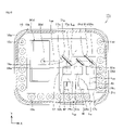
- FIG. 1 is a schematic side view showing the appearance of the optical module according to the first embodiment.
- FIG. 2 is a schematic side view of the optical module shown in FIG. 1 in a state where the cap is removed.
- FIG. 3 is a schematic plan view of the optical module shown in FIG.
- FIG. 4 is an enlarged view showing a part of the optical module shown in FIG. 3 in an enlarged manner.
- FIG. 5 is a schematic plan view showing an enlarged part of the optical module according to the second embodiment.
- FIG. 6 is a schematic perspective view showing a part of the optical module according to the third embodiment in an enlarged manner.
- FIG. 7 is a schematic plan view of the optical module shown in FIG. 6 when cut in a plane including a cap.
- FIG. 8 is a schematic perspective view of the optical module according to the fourth embodiment.
- FIG. 9 is a schematic perspective view of the optical module shown in FIG. 8 with the cap removed.
- FIG. 10 is a schematic plan view of the optical module shown in FIG. 8 when cut in a plane including a cap.
- An optical module including a plurality of semiconductor light emitting elements and a filter for combining light emitted from the plurality of semiconductor light emitting elements can emit light in which light having different wavelengths is combined.
- optical modules are required to be miniaturized. In order to realize the miniaturization of the optical module, it is necessary to miniaturize each component constituting the optical module. Then, at the time of manufacturing the optical module, it is necessary to accurately arrange each of the miniaturized parts. However, it may be difficult for the optical module disclosed in Patent Document 1 to cope with miniaturization.
- one of the purposes is to provide an optical module that can be easily miniaturized.
- the optical module according to one aspect of the present disclosure is configured to emit a first light having a first wavelength and mounted on a base member including a first surface and a first surface.
- a second semiconductor light emitting element configured to emit a second light having a different second wavelength, and a second reflecting surface mounted on the first surface and reflecting the second light. It includes two filters.
- the first light reflected by the first reflecting surface passes through the second filter, and the second reflecting surface reflects the second light, so that the first light and the second light are combined.
- the length of the first filter differs from the length of the second filter.
- a first semiconductor light emitting element, a second semiconductor light emitting element, a first filter and a second filter are mounted on the first surface of the base member.
- a first filter and a second filter are placed on a first surface of a base member on which a first semiconductor light emitting element and a second semiconductor light emitting element are mounted. It is mounted on the surface.
- the first filter and the second filter are adhered to the first surface by using the adhesive applied on the first surface.
- the first filter and the second filter take into consideration the emission direction of the first light emitted from the first semiconductor light emitting element, the emission direction of the second light emitted from the second semiconductor light emitting element, and the like.
- the filter is mounted on the first surface. Specifically, using a jig such as tweezers that sandwiches and grips the filter, first, one of the first filter and the second filter is grasped, and the filter is placed from above the base member. It is mounted on the first surface of the base member. Next, after removing the jig from the filter, the other filter is mounted on the first surface by grasping the other filter with the jig and mounting the other filter from above the base member.
- the optical module is miniaturized, as the miniaturization of each component constituting the optical module progresses, the distance between the first filter and the second filter also becomes narrower. Then, when the filter to be mounted later is attached and the jig is removed, the filter mounted earlier and the jig may interfere with each other. As a result, the position of the previously mounted filter may shift, or the previously mounted filter may be damaged.
- the length of the first filter is different from the length of the second filter in the direction perpendicular to the first plane.
- the filter having the shorter length is first sandwiched and grasped by using the above jig, and the position thereof is adjusted to obtain the desired first surface. It is mounted in the position of.
- the longer filter is sandwiched between jigs and gripped, and the position is adjusted so that the filter is mounted at a desired position on the first surface.
- the length of the filter mounted later is longer than the length of the filter mounted earlier, so the filter and jig mounted earlier will be The possibility of interference can be greatly reduced.
- the first reflecting surface is at least one of light emitted from the second semiconductor light emitting element and transmitted through the second filter and light emitted from the first semiconductor light emitting element and reflected by the second filter. It may be located outside the optical path of one light.
- the second light in the second filter, there is light that is not reflected by the second reflecting surface, although it is a small amount, and the second light partially passes through the second filter.
- the first light in the second filter, there is light that is partially reflected by the first light in a portion that is not the second reflecting surface, although the amount is small.
- the partially transmitted second light or the partially reflected first light reaches the first reflecting surface of the first filter and is reflected, it becomes stray light in the same emission direction as the combined light. there is a possibility. Such a situation is not preferable because stray light may be emitted to the outside of the optical module.
- the first reflecting surface is at least one of light emitted from the second semiconductor light emitting device and transmitted through the second filter and light emitted from the first semiconductor light emitting device and reflected by the second filter. It is located outside the optical path of one light. Therefore, the second light emitted from the second semiconductor light emitting element and not reflected by the second reflecting surface and transmitted through the second filter and the portion emitted from the first semiconductor light emitting element and not the second reflecting surface of the second filter. It is possible to reduce the possibility that the first light reflected in the above reaches the first reflecting surface. Then, the possibility that the second light transmitted through the second filter and the first light reflected by the second filter are reflected by the first reflecting surface and become stray light can be reduced. As a result, the possibility that stray light is emitted to the outside of the optical module can be reduced.
- the distance between the first filter and the second filter may be 0.1 mm or more and 0.3 mm or less. Such an optical module can surely realize miniaturization.
- the optical module may further include a lens that converts the spot size of the first light emitted from the first semiconductor light emitting element or the second light emitted from the second semiconductor light emitting element. By doing so, the first light or the second light having a desired spot size can be emitted from the optical module.
- the optical module may further include a mirror that reflects the light combined by the second filter, and further include a mirror drive mechanism that scans and emits the light combined by the second filter.
- a mirror that reflects the light combined by the second filter
- a mirror drive mechanism that scans and emits the light combined by the second filter.
- the first filter and the second filter may each have a plate shape.
- the length in the direction perpendicular to the thickness direction of the first filter when viewed in the direction perpendicular to the first surface may be shorter than the length in the direction perpendicular to the thickness direction of the second filter.
- the optical module according to another aspect of the present disclosure is configured to emit a first light having a first wavelength and mounted on a base member including a first surface and the first surface.
- a second semiconductor light emitting element configured to emit a second light having a second wavelength different from that of the first surface, and a second reflecting surface mounted on the first surface and reflecting the second light.
- It includes a second filter mounted on the first surface and including a third reflecting surface that reflects the third light.
- the first filter is arranged between the second filter and the third filter when viewed in the direction perpendicular to the first plane.
- the first light reflected by the first reflecting surface passes through the second filter, the second reflecting surface reflects the second light, and the third light reflected by the third reflecting surface is the third.
- the first filter and the second filter By passing through the first filter and the second filter, the first light, the second light, and the third light are combined.
- the length of the first filter is longer than the length of the second filter and the length of the third filter.
- a filter having a length shorter than that of the first filter that is, a second filter
- it is grasped by sandwiching any of the third filters, its position is adjusted, and it is mounted at a desired position on the first surface.
- another filter having a length shorter than that of the first filter is sandwiched and grasped, the position thereof is adjusted, and the filter is mounted at a desired position on the first surface.
- the filter having the longest length that is, the first filter is sandwiched by a jig and grasped, and the position thereof is adjusted to mount the filter at a desired position on the first surface.
- the length of the first filter mounted later is longer than the length of the second filter and the third filter mounted earlier, so that the second filter and the third filter are used. The possibility of interference with the jig can be greatly reduced.
- FIG. 1 is a schematic side view showing the appearance of the optical module according to the first embodiment.
- FIG. 2 is a schematic side view of the optical module shown in FIG. 1 in a state where the cap is removed.
- FIG. 3 is a schematic plan view of the optical module shown in FIG.
- FIG. 4 is an enlarged view showing a part of the optical module shown in FIG. 3 in an enlarged manner.
- the optical module 11a includes a substrate 12, a base member 13, a cap 14a, a plurality of lead pins 15a, and light forming light.
- the forming portion 20a and the like are included.
- the substrate 12 has a disk shape.
- the substrate 12 includes a first main surface 12a of the substrate 12 and a second main surface 12b different from the first main surface 12a of the substrate 12.
- the first main surface 12a and the second main surface 12b are along the XX plane.
- the plurality of lead pins 15a penetrate from the first main surface 12a to the second main surface 12b.
- Each of the plurality of lead pins 15a is provided so as to extend in the Y direction.
- Each of the plurality of lead pins 15a is electrically connected to each component constituting the light forming portion 20a described later, such as the first semiconductor light emitting element 41, by wiring or the like (not shown).
- the base member 13 has a flat plate shape.
- the base member 13 is connected to a first surface 13a of the base member 13, a second surface 13b different from the first main surface 13a of the base member 13, and a first surface 13a and a second surface 13b.
- the third surface 13c and the like are included.
- the first surface 13a and the second surface 13b are respectively along the XY plane.
- the third surface 13c is along the XX plane.
- Each component constituting the light forming portion 20a is mounted on the first surface 13a of the base member 13.
- the base member 13 is arranged so that the third surface 13c is in contact with the first main surface 12a of the substrate 12.
- the cap 14a is a lid portion welded to the substrate 12.
- the cap 14a is arranged in contact with the first main surface 12a so as to cover the light forming portion 20a and the base member 13. That is, the light forming portion 20a and the base member 13 are arranged in the space surrounded by the substrate 12 and the cap 14a.
- the cap 14a is formed with an exit window 14b through which light from the light forming portion 20a is transmitted.
- the exit window 14b is made of glass and is provided with a transmission plate through which light is transmitted.
- the light forming unit 20a is a first semiconductor light emitting element configured to emit a first light having a first wavelength, a first base block 21a, a second base block 22a, and a third base block 23a. 41, a second semiconductor light emitting element 42 configured to emit a second light having a second wavelength, and a third semiconductor configured to emit a third light having a third wavelength.
- the light emitting element 43, the first filter 61a, and the second filter 71a are included.
- the light formed by the light forming unit 20a passes through the exit window 14b and is emitted to the outside of the optical module 11a.
- the first semiconductor light emitting element 41 is a green laser diode
- the second semiconductor light emitting element 42 is a blue laser diode
- the third semiconductor light emitting element 43 is a red laser diode. Therefore, the first light having the first wavelength is green light, the second light having the second wavelength is the blue light, and the third light having the third wavelength is the red light. Is.
- the first base block 21a, the second base block 22a, and the third base block 23a are respectively arranged on the first surface 13a of the base member 13 at intervals.
- the first semiconductor light emitting element 41 is arranged on the first base block 21a.
- the second semiconductor light emitting element 42 is arranged on the second base block 22a.
- the third semiconductor light emitting element 43 is arranged on the third base block 23a.
- the first semiconductor light emitting element 41, the second semiconductor light emitting element 42, and the third semiconductor light emitting element 43 are mounted on the first surface 13a.
- the emission direction of green light by the first semiconductor light emitting element 41 and the emission direction of blue light by the second semiconductor light emitting element 42 are both in the X direction.
- the emission direction of the red light by the third semiconductor light emitting element 43 is the Y direction orthogonal to the emission direction of the green light by the first semiconductor light emitting element 41 and the emission direction of the blue light by the second semiconductor light emitting element 42. That is, the optical axis L 13 of the red light, the optical axis L 11 of the green light, and the optical axis L 12 of the blue light are orthogonal to each other.
- the first filter 61a and the second filter 71a are, for example, wavelength selectivity filters.
- the first filter 61a and the second filter 71a are dielectric multilayer filters.
- the red light passes through the first filter 61a, and the first filter 61a reflects the green light.
- the red light and the green light pass through the second filter 71a, and the second filter 71a reflects the blue light.
- the first filter 61a has a flat plate shape.
- the first filter 61a has a rectangular shape when viewed in the thickness direction.
- the thickness direction of the filter is the direction along the XY plane.
- the first filter 61a includes a transparent plate-shaped member 62a and a dielectric multilayer film 63a.
- the material of the plate-shaped member 62a for example, glass, specifically, Pyrex (registered trademark), quartz, BK7 (registered trademark), Tempax (registered trademark) and the like are used.
- the dielectric multilayer film 63a is provided on one of two surfaces of the plate-shaped member 62a in the thickness direction.
- the first filter 61a includes a first reflecting surface 64a which is a first surface, a second surface 65a different from the first reflecting surface, a third surface 66a, a fourth surface 67a, and a first surface.
- the fifth surface 68a and the sixth surface 69a are included.
- the third surface 66a, the fourth surface 67a, the fifth surface 68a, and the sixth surface 69a are connected to the first reflecting surface 64a and the second surface 65a, respectively.
- the third surface 66a and the fourth surface 67a are respectively along the XY plane.
- the first reflecting surface 64a and the second surface 65a are parallel to each other.
- the third surface 66a and the fourth surface 67a are parallel to each other.
- the fifth surface 68a and the sixth surface 69a are parallel to each other.
- the fifth surface 68a is a plane perpendicular to the first reflecting surface 64a, the second surface 65a, the third surface 66a, and the fourth surface 67a, respectively.
- the sixth surface 69a is a plane perpendicular to the first reflecting surface 64a, the second surface 65a, the third surface 66a, and the fourth surface 67a, respectively.
- the dielectric multilayer film 63a is configured to include a first reflecting surface 64a.
- the first reflecting surface 64a is a surface that reflects green light, which is the first light having a first wavelength. That is, the first filter 61a includes a first reflecting surface 64a that reflects green light, which is the first light. Further, the red light, which is the third light having the third wavelength, passes through the first filter 61a.
- the second filter 71a has a flat plate shape.
- the second filter 71a has a rectangular shape when viewed in the thickness direction.
- the second filter 71a includes a transparent plate-shaped member 72a and a dielectric multilayer film 73a.
- As the material of the plate-shaped member 72a the same material as that of the plate-shaped member 62a is adopted.
- the dielectric multilayer film 73a is provided on one of two surfaces of the plate-shaped member 72a in the thickness direction.
- the second filter 71a includes a second reflecting surface 74a, which is a first surface, a second surface 75a different from the first surface, a third surface 76a, a fourth surface 77a, and a fifth surface.
- Surface 78a and a sixth surface 79a are examples of the plate-shaped member 72a.
- the third surface 76a, the fourth surface 77a, the fifth surface 78a, and the sixth surface 79a are connected to the second reflecting surface 74a and the second surface 75a, respectively.
- the third surface 76a and the fourth surface 77a are respectively along the XY plane.
- the second reflecting surface 74a and the second surface 75a are parallel to each other.
- the third surface 76a and the fourth surface 77a are parallel.
- the fifth surface 78a and the sixth surface 79a are parallel to each other.
- the fifth surface 78a is a plane perpendicular to the second reflecting surface 74a, the second surface 75a, the third surface 76a, and the fourth surface 77a, respectively.
- the sixth surface 79a is a plane perpendicular to the second reflecting surface 74a, the second surface 75a, the third surface 76a, and the fourth surface 77a, respectively.
- the dielectric multilayer film 73a is configured to include a second reflecting surface 74a.
- the second reflecting surface 74a is a surface that reflects blue light, which is the second light having a second wavelength. That is, the second filter 71a includes a second reflecting surface 74a that reflects blue light, which is the second light. Further, the green light which is the first light and the red light which is the third light pass through the second filter 71a.
- the first filter 61a and the second filter 71a are mounted on the first surface 13a. Specifically, the fourth surface 67a and the first surface 13a of the first filter 61a are arranged so as to face each other. Further, the fourth surface 77a and the first surface 13a of the second filter 71a are arranged so as to face each other.
- the first filter 61a and the second filter 71a are attached to the first surface 13a by using an adhesive composed of an ultraviolet curable resin or the like.
- the length of the first filter 61a is different from the length of the second filter 71a.
- the length H 1 of the first filter 61a which is the distance between the third surface 66a and the fourth surface 67a of the first filter 61a shown in FIG. 2, is the third of the second filter 71a. It is longer than the length H2 of the second filter 71a, which is the distance between the surface 76a and the fourth surface 77a.
- the first filter 61a and the second filter 71a have the same rectangular shape when viewed in the thickness direction, and the first filter 61a has a so-called lateral orientation in which the longitudinal direction is attached to the first surface 13a.
- the second filter 71a is in a so-called vertical orientation state in which the lateral direction is attached to the first surface 13a.
- the first filter 61a is arranged at a position on the first reflecting surface 64a that reflects green light and transmits red light.
- the second filter 71a is arranged on the second reflecting surface 74a at a position where blue light is reflected and green light and red light are transmitted.
- the first reflecting surface 64a of the first filter 61a and the second reflecting surface 74a of the second filter 71a are directed with respect to the emission directions of the light emitted from the first semiconductor light emitting element 41 and the second semiconductor light emitting element 42, respectively. It is inclined.
- the first reflecting surface 64a of the first filter 61a and the second reflecting surface 74a of the second filter 71a are green colors emitted from the first semiconductor light emitting element 41 and the second semiconductor light emitting element 42, respectively.
- the first reflecting surface 64a of the first filter 61a and the second reflecting surface 74a of the second filter 71a are the optical axes L13 of red light emitted from the third semiconductor light emitting device 43, respectively. It is also tilted 45 ° with respect to.
- the first filter 61a and the second filter 71a combine the light emitted from the first semiconductor light emitting element 41, the second semiconductor light emitting element 42, and the third semiconductor light emitting element 43.
- the optical axis L 14 of the combined light is configured to pass through the exit window 14b.
- the light emitted from the first semiconductor light emitting element 41, the second semiconductor light emitting element 42, and the third semiconductor light emitting element 43 is diffused light, respectively.
- the optical path diffused toward the first semiconductor light emitting device 41 is indicated by the optical path L15 .
- the first reflecting surface 64a is located outside the optical path L 16 of blue light emitted from the second semiconductor light emitting device 42 along the optical path L 15 and transmitted through the second filter 71a.
- the length D 1 in the direction perpendicular to the thickness direction of the first filter 61a when viewed in the direction perpendicular to the first surface 13a is the direction perpendicular to the thickness direction of the second filter 71a. Is shorter than the length D 2 .
- the first reflecting surface 64a is configured to be located outside the optical path L 16 of the blue light emitted from the second semiconductor light emitting element 42 and transmitted through the second filter 71a.
- the distance D 3 between the first filter 61a and the second filter 71a is 0.1 mm or more and 0.3 mm or less.
- the distance D3 between the first filter 61a and the second filter 71a is the distance between the first reflecting surface 64a of the first filter 61a and the second surface 75a of the second filter 71a.
- the adhesive is applied to a predetermined position on the first surface 13a of the base member 13, specifically, a desired position to attach the first filter 61a and a desired position to attach the second filter 71a.
- the first filter 61a and the second filter 71a are attached on the adhesive, and the first filter 61a and the second filter 71a are mounted on the first surface 13a of the base member 13.
- the second filter 71a having a short length H2 is attached first.
- the upper portion of the second filter 71a that is, the region close to the third surface 76a is chucked and lifted by a jig so as to be sandwiched in the thickness direction of the second filter 71a.
- the second filter 71a is attached to the attachment position of the second filter 71a.
- the position of the second reflecting surface 74a is the blue light emitted by the second semiconductor light emitting element 42 and the green light emitted by the first semiconductor light emitting element 41 and reflected by the first reflecting surface 64a.
- the second filter 71a is attached so as to be located at a portion where the light of the above and the red light emitted by the third semiconductor light emitting element 43 intersect. After that, the jig is opened in the thickness direction of the second filter 71a, and the jig is removed from the second filter 71a.
- a long first filter 61a having a length H1 is attached. Also in this case, the upper portion of the first filter 61a, that is, the region close to the third surface 66a is chucked and lifted by a jig so as to be sandwiched in the thickness direction of the first filter 61a. Then, the first filter 61a is attached to the attachment position of the first filter 61a. Specifically, the position of the first reflecting surface 64a is located at the intersection of the green light emitted by the first semiconductor light emitting element 41 and the red light emitted by the third semiconductor light emitting element 43. The first filter 61a is attached to the.
- the jig is opened in the thickness direction of the first filter 61a, and the jig is removed from the first filter 61a.
- the adhesive is cured, a plurality of lead pins 15a are attached to the substrate 12, wiring to the lead pins 15a and the like are performed, and finally a cap 14a is attached. In this way, the optical module 11a is assembled and manufactured.
- the length H 1 of the first filter 61a is different from the length H 2 of the second filter 71a in the direction perpendicular to the first surface 13a.
- the shorter filter in this case the second filter 71a
- the position thereof is determined. It is adjusted and mounted at a desired position on the first surface 13a.
- the longer filter in this case the first filter 61a
- the position thereof is adjusted so that the filter is mounted at a desired position on the first surface 13a.
- the length H 1 of the first filter mounted later is larger than the length H 2 of the second filter 71a mounted earlier. Since it is long, the possibility that the second filter 71a mounted first and the jig interfere with each other can be greatly reduced. Therefore, when the first filter 61a is mounted later, there is a high possibility that the second filter 71a mounted earlier and the jig come into contact with each other and the position of the second filter 71a mounted earlier is displaced or damaged. Can be reduced. Therefore, it is possible to reduce the labor in manufacturing each of the miniaturized parts, which requires careful work when the first filter 61a is mounted later. As a result, according to the optical module 11a, it becomes easy to reduce the size.
- the second filter 71a includes a second reflecting surface 74a that reflects blue light, which is the second light emitted from the second semiconductor light emitting element 42.
- the second filter 71a there is light that is not reflected by the second reflecting surface 74a and is partially transmitted through the second filter 71a by blue light, which is the second light.
- the partially transmitted blue light reaches the first reflecting surface 64a of the first filter 61a and is reflected, there is a possibility that the light is stray light in the same emission direction as the combined light. Such a situation is not preferable because stray light may be emitted to the outside of the optical module 11a.
- the first reflecting surface 64a is located outside the optical path L 16 of blue light emitted from the second semiconductor light emitting element 42 along the optical path L 15 and transmitted through the second filter 71a. It is possible to reduce the possibility that the blue light that has not been reflected by the reflection surface 74a of the second and has passed through the second filter 71a reaches the first reflection surface 64a. Then, the possibility that the blue light transmitted through the second filter 71a is reflected by the first reflecting surface 64a and becomes stray light can be reduced. As a result, the possibility that the stray light is emitted to the outside of the optical module 11a can be reduced.
- the distance D3 between the first filter 61a and the second filter 71a is 0.1 mm or more and 0.3 mm or less. Such an optical module 11a can surely realize miniaturization.
- the length D 1 in the direction perpendicular to the thickness direction of the first filter 61a when viewed in the direction perpendicular to the first surface 13a is the direction perpendicular to the thickness direction of the second filter 71a. Shorter than length D 2 . Therefore, it becomes easy to position the first reflecting surface outside the optical path L 16 of the blue light emitted from the second semiconductor light emitting device 42 along the optical path L 15 and transmitted through the second filter 71a. Therefore, it becomes easy to reduce the possibility of stray light.
- the first reflecting surface 64a is located outside the optical path L 16 of light emitted from the second semiconductor light emitting element 42 along the optical path L 15 and transmitted through the second filter 71a.
- the present invention is not limited to this, and the first reflecting surface 64a is located outside the optical path L 18 of the light emitted from the first semiconductor light emitting element 41 along the optical path L 17 and reflected by the second filter 71a. May be good.
- the optical path diffused toward the third semiconductor light emitting device 43 is indicated by the optical path L17 .
- the first reflecting surface 64a is at least one of the light emitted from the second semiconductor light emitting element 42 and transmitted through the second filter 71a and the light emitted from the first semiconductor light emitting element 41 and reflected by the second filter 71a. It may be located outside the optical path of one light. By doing so, the blue light, which is the second light emitted from the second semiconductor light emitting element 42, is not reflected by the second reflecting surface 74a, and is transmitted through the second filter 71a, and the first semiconductor light emitting element 41. Reduces the possibility that at least one of the green light, which is the first light emitted and reflected at the portion of the second filter 71a other than the second reflecting surface 74a, reaches the first reflecting surface 64a. can do.
- the blue light emitted from the second semiconductor light emitting device 42 and transmitted through the second filter 71a and the green light emitted from the first semiconductor light emitting element 41 and reflected by the second filter 71a are emitted by the first reflecting surface 64a. It is possible to reduce the possibility of being reflected and becoming stray light. As a result, the possibility that the stray light is emitted to the outside of the optical module 11a can be reduced.
- FIG. 5 is a schematic plan view showing an enlarged part of the optical module according to the second embodiment.
- the configuration of the first filter is different from that of the first embodiment.
- the first filter 61b when viewed in a direction perpendicular to the first surface 13a (that is, in the XY plane), the first filter 61b
- the length D 4 in the direction perpendicular to the thickness direction is longer than the length D 2 in the direction perpendicular to the thickness direction of the second filter 71a.
- the first filter 61b includes a first reflection surface 64b, which is a first surface, a second surface 65b different from the first surface, a third surface 66b, a fourth surface 67b, and a fifth surface.
- the length D 4 is the length from the fifth surface 68b to the sixth surface 69b.
- the dielectric multilayer film 63b included in the first filter 61b is not provided on the entire surface of any one of the two surfaces in the thickness direction of the plate-shaped member 62b, but is provided on a part thereof. ing.
- the first filter 61b includes a plate-shaped member 62b and a dielectric multilayer film 63b.
- the plate-shaped member 62b includes a region 70b on the first reflecting surface 64b side on which the dielectric multilayer film 63b is not formed.
- the region 70b is a portion where the plate-shaped member 62b is arranged as it is, and in the region 70b, light is transmitted without being reflected.
- the first reflecting surface 64b can be positioned outside the optical path L 16 of the blue light emitted from the second semiconductor light emitting device 42. Therefore, in the region 70b, the blue light emitted from the second semiconductor light emitting device 42 along the optical path L15 and transmitted through the second filter 71a reaches the first filter 61b, and the light that reaches reaches the first filter 61b. The possibility of reflection can be reduced. Therefore, the possibility of stray light can be reduced.
- FIG. 6 is a schematic perspective view showing a part of the optical module according to the third embodiment in an enlarged manner.
- FIG. 7 is a schematic plan view of the optical module shown in FIG. 6 when cut in a plane including a cap.
- the optical module of the third embodiment is different from the case of the first embodiment in that it includes a lens, a TEC (Thermo-Electric Cooler), and the like. Note that in FIG. 6, the cap included in the optical module is not shown.
- the optical module 11c of the third embodiment includes a substrate 16, a base member 17, a cap 18a, a plurality of lead pins 15c, and an optical forming portion 20c that forms light. include.
- the substrate 16 has a flat plate shape.
- the substrate 16 includes a first main surface 16a of the substrate 16 and a second main surface 16b different from the first main surface 16a of the substrate 16.
- the first main surface 16a and the second main surface 16b are along the XY plane.
- the plurality of lead pins 15c penetrate from the first main surface 16a to the second main surface 16b.
- Each of the plurality of lead pins 15c is provided so as to extend in the Z direction.
- Each of the plurality of lead pins 15c is electrically connected to each component constituting the light forming portion 20c described later, such as the first semiconductor light emitting element 41.
- the base member 17 has a flat plate shape.
- the base member 17 includes a first surface 17a of the base member 17 and a second surface 17b different from the first surface 17a of the base member 17.
- the first surface 17a and the second surface 17b are respectively along the XY plane.
- Each component constituting the light forming portion 20c is mounted on the first surface 17a of the base member 17.
- the optical module 11c includes a TEC 31c which is an electronic cooling module.
- the TEC 31c includes a heat radiating plate 32c, a heat absorbing plate 33c, and a plurality of semiconductor columns 34c.
- the heat radiating plate 32c and the heat absorbing plate 33c each have a flat plate shape.
- the heat radiating plate 32c and the heat absorbing plate 33c are arranged apart from each other in the thickness direction of the base member 17.
- the plurality of semiconductor columns 34c are arranged at intervals.
- the plurality of semiconductor columns 34c are attached so that one end is connected to the heat sink 32c and the other end is connected to the endothermic plate 33c.
- the TEC 31c is arranged between the substrate 16 and the base member 17.
- the TEC 31c is arranged so that the first main surface 16a of the substrate 16 and the heat radiating plate 32c are in contact with each other, and the second surface 17b of the base member 17 and the heat absorbing plate 33c are in contact with each other.
- the heat of the base member 17 is transferred to the substrate 16 side, and the temperature of the base member 17 and each component constituting the light forming portion 20c is adjusted by cooling or the like.
- the light forming unit 20c includes a first base block 21c, a second base block 22c, a first semiconductor light emitting element 41, a second semiconductor light emitting element 42, a third semiconductor light emitting element 43, a first filter 61a, and the like.
- the second filter 71a, the first lens 51c, the second lens 52c, and the third lens 53c are included.
- the first lens 51c is arranged between the first semiconductor light emitting element 41 and the first filter 61a when viewed in the thickness direction of the base member 17.
- the first lens 51c converts the spot size of green light, which is the first light emitted from the first semiconductor light emitting device.
- the first lens 51c converts the diffused light emitted from the first semiconductor light emitting device 41 into collimated light.
- the second lens 52c is arranged between the second semiconductor light emitting element 42 and the second filter 71a when viewed in the thickness direction of the base member 17.
- the second lens 52c converts the spot size of blue light, which is the second light emitted from the second semiconductor light emitting device 42.
- the second lens 52c converts the diffused light emitted from the second semiconductor light emitting device 42 into collimated light.
- the third lens 53c is arranged between the third semiconductor light emitting element 43 and the first filter 61a when viewed in the thickness direction of the base member 17.
- the third lens 53c converts the spot size of red light, which is the third light emitted from the third semiconductor light emitting device 43.
- the third lens 53c converts the diffused light emitted from the third semiconductor light emitting device 43 into collimated light. By doing so, green light, blue light, and red light having a desired spot size can be emitted from the optical module 11c.
- the light formed by the light forming unit 20c passes through the exit window 18b and is emitted to the outside of the optical module 11c.
- the first base block 21c and the second base block 22c are respectively arranged on the first surface 17a of the base member 17 at intervals.
- the first submount 24c and the second submount 25c are arranged on the first base block 21c.
- the first semiconductor light emitting element 41 is arranged on the first submount 24c.
- the second semiconductor light emitting element 42 is arranged on the second submount 25c.
- the third submount 26c is arranged on the second base block 22c.
- the third semiconductor light emitting device 43 is arranged on the third submount 26c.
- the first semiconductor light emitting element 41, the second semiconductor light emitting element 42, and the third semiconductor light emitting element 43 are mounted on the first surface 13a.
- the emission direction of green light by the first semiconductor light emitting element 41 and the emission direction of blue light by the second semiconductor light emitting element 42 are both in the X direction. That is, the optical axis L 31 of green light and the optical axis L 32 of blue light are parallel to each other.
- the emission direction of the red light by the third semiconductor light emitting element 43 is the Y direction orthogonal to the emission direction of the green light by the first semiconductor light emitting element 41 and the emission direction of the blue light by the second semiconductor light emitting element 42. That is, the optical axis L 33 of the red light, the optical axis L 31 of the green light, and the optical axis L 32 of the blue light are orthogonal to each other.
- the first filter 61a and the second filter 71a are mounted on the first surface 17a.
- the first filter 61a and the second filter 71a are attached to the first surface 17a by using an adhesive composed of an ultraviolet curable resin or the like.
- the length of the first filter 61a is different from the length of the second filter 71a in the direction perpendicular to the first surface 17a. Specifically, the length of the first filter 61a in the direction perpendicular to the first surface 17a is longer than the length of the second filter 71a in the direction perpendicular to the first surface 17a.
- the first filter 61a is arranged at a position on the first reflecting surface 64a that reflects green light and transmits red light.
- the second filter 71a is arranged on the second reflecting surface 74a at a position where blue light is reflected and green light and red light are transmitted.
- the first reflecting surface 64a of the first filter 61a and the second reflecting surface 74a of the second filter 71a are directed with respect to the emission directions of the light emitted from the first semiconductor light emitting element 41 and the second semiconductor light emitting element 42, respectively. It is inclined.
- the first reflecting surface 64a of the first filter 61a and the second reflecting surface 74a of the second filter 71a are green colors emitted from the first semiconductor light emitting element 41 and the second semiconductor light emitting element 42, respectively.
- the first reflecting surface 64a of the first filter 61a and the second reflecting surface 74a of the second filter 71a are the optical axes L 33 of the red light emitted from the third semiconductor light emitting device 43, respectively. It is also tilted 45 ° with respect to.
- the first filter 61a and the second filter 71a combine the light emitted from the first semiconductor light emitting element 41, the second semiconductor light emitting element 42, and the third semiconductor light emitting element 43.
- the optical axis L 34 of the combined light is configured to pass through the exit window 18b.
- the light emitted from the first semiconductor light emitting element 41, the second semiconductor light emitting element 42, and the third semiconductor light emitting element 43 is diffused light, respectively.
- the optical path diffused toward the third semiconductor light emitting device 43 is indicated by the optical path L35 .
- the green light emitted from the first semiconductor light emitting device 41 along the optical path L 35 travels along the optical path L 36 through the first lens 51c and is reflected by the first reflecting surface 64a of the first filter 61a. do. After that, it proceeds along the optical path L37 . Then, a small amount of light traveling along the optical path L 37 is reflected by the second surface 75a of the second filter 71a.
- the first reflecting surface 64a is located outside the optical path L 38 of green light emitted from the first semiconductor light emitting device 41 and reflected by the second surface 75a of the second filter 71a.
- the length in the direction perpendicular to the thickness direction of the first filter 61a when viewed in the direction perpendicular to the first surface 17a is the length in the direction perpendicular to the thickness direction of the second filter 71a. Shorter than that.
- the first reflecting surface 64a is located outside the optical path L 38 of the green light emitted from the first semiconductor light emitting element 41 and reflected by the second surface 75a of the second filter 71a. Has been done.
- the TEC 31a is adhered onto the first main surface 16a of the substrate 16.
- the semiconductor light emitting element 43 adheres the substrate 16 provided on the base member 17 onto the TEC 31a.
- the adhesive is applied to a predetermined position on the first surface 17a of the base member 17, specifically, a desired position to attach the first filter 61a and a desired position to attach the second filter 71a.
- the first filter 61a and the second filter 71a are attached on the adhesive, and the first filter 61a and the second filter 71a are mounted on the first surface 17a of the base member 17.
- the second filter 71a is attached.
- the upper portion of the second filter 71a is chucked and lifted by a jig so as to be sandwiched in the thickness direction of the second filter 71a.
- the second filter 71a is attached to the attachment position of the second filter 71a.
- the position of the second reflecting surface 74a is emitted by the blue light emitted by the second semiconductor light emitting element 42 and emitted by the first semiconductor light emitting element 41, and is reflected by the first reflecting surface 64a.
- the second filter 71a is attached so as to be located at a portion where the green light and the red light emitted by the third semiconductor light emitting element 43 intersect. After that, the jig is opened in the thickness direction of the second filter 71a, and the jig is removed from the second filter 71a.
- the first filter 61a attaches the first filter 61a. Also in this case, the upper portion of the first filter 61a is chucked and lifted by a jig so as to be sandwiched in the thickness direction of the first filter 61a. Then, the first filter 61a is attached to the attachment position of the first filter 61a. Specifically, the position of the first reflecting surface 64a is located at the intersection of the green light emitted by the first semiconductor light emitting element 41 and the red light emitted by the third semiconductor light emitting element 43. The first filter 61a is attached to the. After that, the jig is opened in the thickness direction of the first filter 61a, and the jig is removed from the first filter 61a. Next, the adhesive is cured. After that, a plurality of lead pins 15c are attached to the substrate 16, wiring to the lead pins 15c and the like are performed, and finally the cap 18a is attached. In this way, the optical module 11c is assembled and manufactured.
- the length of the first filter 61a is different from the length of the second filter 71a in the direction perpendicular to the first surface 17a.
- the shorter filter in this case the second filter 71a
- the position thereof is determined. It is adjusted and mounted at a desired position on the first surface 13a.
- the longer filter in this case the first filter 61a
- the position thereof is adjusted so that the filter is mounted at a desired position on the first surface 13a.
- the length of the first filter 61a, which is mounted later, is longer than the length of the second filter 71a, which is mounted first.
- the possibility of interference between the second filter 71a mounted on the jig and the jig can be greatly reduced. Therefore, when the first filter 61a is mounted later, there is a high possibility that the second filter 71a mounted earlier and the jig come into contact with each other and the position of the second filter 71a mounted earlier is displaced or damaged. Can be reduced. Therefore, it is possible to reduce the labor in manufacturing each of the miniaturized parts, which requires careful work when the first filter 61a is mounted later. As a result, according to the optical module 11c, it becomes easy to reduce the size.
- the first reflecting surface 64a is located outside the optical path L 38 of the green light emitted from the first semiconductor light emitting element 41 and reflected by the second surface 75a of the second filter 71a.
- the portion of the 2 filter 71a that is not the second reflecting surface 74a, in this case, the green light that is reflected on the second surface 75a and travels along the optical path L 38 may reach the first reflecting surface 64a. Can be reduced.
- the green light reflected by the second filter 71a is reflected by the first reflecting surface 64a, and the possibility of becoming stray light can be reduced. As a result, the possibility that the stray light is emitted to the outside of the optical module 11c can be reduced.
- FIG. 8 is a schematic perspective view of the optical module according to the fourth embodiment.
- FIG. 9 is a schematic perspective view of the optical module shown in FIG. 8 with the cap removed.
- FIG. 10 is a schematic plan view of the optical module shown in FIG. 8 when cut in a plane including a cap.
- the optical module of the fourth embodiment is different from the case of the third embodiment in that it includes a mirror drive mechanism and the like. Note that in FIG. 9, the cap included in the optical module is not shown.
- the optical module 11d of the fourth embodiment includes a substrate 16, a base member 17, a cap 19a provided with an exit window 19b, a plurality of lead pins 15c, and a TEC 31c. And a light forming unit 20d that forms light. Each component constituting the light forming portion 20d is mounted on the first surface 17a of the base member 17.
- the light forming unit 20d includes a first base block 21c, a first semiconductor light emitting element 41, a second semiconductor light emitting element 42, a third semiconductor light emitting element 43, a first filter 61a, a second filter 71a, and a second.
- the 3 filter 81d, the first lens 51c, the second lens 52c, and the third lens 53c are included.
- the first filter 61a is arranged so that the first reflecting surface 64a is located outside the optical path L 45 of green light emitted from the first semiconductor light emitting device 41 and reflected by the second surface 75a of the second filter 71a. ing.
- the third filter 81d is, for example, a wavelength selectivity filter.
- the third filter 81d is a dielectric multilayer filter.
- the third filter 81d reflects red light, which is light having a third wavelength emitted from the third semiconductor light emitting device 43.
- the third filter 81d has a flat plate shape.
- the third filter 81d has a rectangular shape when viewed in the thickness direction. Since the configuration of the third filter 81d is the same as the configuration of the second filter 71a except that the wavelength of the reflected light is different, the description thereof will be omitted.
- the third lens 53c is arranged between the third semiconductor light emitting element 43 and the third filter 81d when viewed in the thickness direction of the base member 17.
- the third filter 81d is mounted on the first surface 17a.
- the third filter 81d is attached next to the first filter 61a in the X direction. That is, the first filter 61a is arranged between the second filter 71a and the third filter 81d in the X direction. In other words, the first filter 61a is arranged between the second filter 71a and the third filter 81d when viewed in the direction perpendicular to the first surface 17a of the base member 17.
- the third filter 81d is attached to the first surface 17a using an adhesive composed of an ultraviolet curable resin or the like.
- the first base block 21c is arranged on the first surface 17a of the base member 17.
- the first submount 24c, the second submount 25c, and the third submount 26c are arranged on the first base block 21c.
- the first semiconductor light emitting element 41 is arranged on the first submount 24c.
- the second semiconductor light emitting element 42 is arranged on the second submount 25c.
- the third semiconductor light emitting device 43 is arranged on the third submount 26c.
- the first semiconductor light emitting element 41, the second semiconductor light emitting element 42, and the third semiconductor light emitting element 43 are mounted on the first surface 13a.
- the emission direction of green light by the first semiconductor light emitting element 41, the emission direction of blue light by the second semiconductor light emitting element 42, and the emission direction of red light by the third semiconductor light emitting element 43 are all in the X direction. Is. That is, the optical axis L 41 of green light, the optical axis L 42 of blue light, and the optical axis L 43 of red light are parallel to each other.
- the length of the first filter 61a is different from the length of the third filter 81d in the direction perpendicular to the first surface 17a. Specifically, the length of the first filter 61a in the direction perpendicular to the first surface 17a is longer than the length of the third filter 81d in the direction perpendicular to the first surface 17a. Further, in the present embodiment, the length of the first filter 61a in the direction perpendicular to the first surface 17a is longer than the length of the second filter 71a in the direction perpendicular to the first surface 17a. That is, in the direction perpendicular to the first surface 17a, the length of the first filter 61a is longer than the length of the second filter 71a and the length of the third filter 81d.
- the third filter 81d is arranged at a position on the third reflecting surface 84d to reflect red light.
- the third reflecting surface 84d of the third filter 81d is inclined with respect to the emission direction of the light emitted from the third semiconductor light emitting device 43.
- the third reflecting surface 84d of the third filter 81d is inclined by 45 ° with respect to the optical axis L 43 of the red light emitted from the third semiconductor light emitting device 43.
- the light forming unit 20d included in the optical module 11d includes a mirror drive mechanism 91d.
- the mirror drive mechanism 91d includes a mirror 92d that reflects the light combined by the second filter 71a.
- the mirror drive mechanism 91d is arranged on the TEC 31c. Specifically, the mirror drive so that the light of the optical axis L 44 combined by the second filter 71a hits the swinging mirror 92d and is reflected, and the reflected light can be emitted from the exit window 19b.
- the mechanism 91d is arranged.
- the mirror drive mechanism 91d scans and emits the light combined with the second filter 71a.
- the light formed by the light forming unit 20d passes through the exit window 19b and is emitted to the outside of the optical module 11d.
- the optical module 11d scans the combined light of the first light, the green light, the second light, the blue light, and the third light, the red light, along a desired path. , Characters and figures can be drawn.
- the length of the first filter 61a is different from the length of the second filter 71a in the direction perpendicular to the first surface 17a.
- the filter having the shorter length is first used, and in this case, the second filter 71a or the third filter 81d. Any one of the filters 81d, for example, the second filter 71a is sandwiched and grasped, and the position thereof is adjusted so that the filter 81d is mounted at a desired position on the first surface 13a.
- the third filter 81d is sandwiched and grasped, the position thereof is adjusted, and the third filter 81d is mounted at a desired position on the first surface 13a.
- the distance between the third filter 81d, which is mounted later, and the second filter 71a is large, so that the second filter 71a, which is mounted first, is large.
- the possibility of interference between the jig and the jig can be greatly reduced.
- the longer filter in this case the first filter 61a, is sandwiched between jigs and gripped, and the position thereof is adjusted so that the filter is mounted at a desired position on the first surface 13a.
- the length of the first filter 61a, which is mounted later, is larger than the length of the second filter 71a and the third filter 81d, which are mounted first. Therefore, the possibility of interference between the first-mounted second filter 71a and third filter 81d and the jig can be greatly reduced. Therefore, when the first filter 61a is mounted later, the second filter 71a and the third filter 81d mounted earlier come into contact with the jig, and the position of the second filter 71a or the third filter 81d mounted earlier comes into contact with each other. The possibility of slippage or damage can be greatly reduced. Therefore, it is possible to reduce the labor in manufacturing each of the miniaturized parts, which requires careful work when the first filter 61a is mounted later. As a result, according to the optical module 11d, it becomes easy to reduce the size.
- the first reflecting surface 64a is located outside the optical path L 45 of green light emitted from the first semiconductor light emitting device 41 and reflected by the second surface 75a of the second filter 71a. 1 A portion of the second filter 71a that is not the second reflecting surface 74a emitted from the semiconductor light emitting device 41, in this case, the green light reflected on the second surface 75a can reach the first reflecting surface 64a. The sex can be reduced. Then, the green light emitted from the first semiconductor light emitting element 41 and reflected by the second filter 71a is reflected by the first reflecting surface 64a, and the possibility of becoming stray light can be reduced. As a result, the possibility that the stray light is emitted to the outside of the optical module 11d can be reduced.
- the optical module includes a first semiconductor light emitting device, a second semiconductor light emitting element, and a third semiconductor light emitting element, but the optical module is not limited to this. It may be configured not to include the third semiconductor light emitting element. In this case, the combination of the first semiconductor light emitting element and the second semiconductor light emitting element may be light having different wavelengths.
- 11a, 11b, 11c, 11d Optical module, 12,16 substrate, 12a, 16a first main surface, 12b, 16b second main surface, 13,17 base member, 13a, 17a first surface, 13b, 17b , 65a, 65b, 75a second surface, 13c, 66a, 66b, 76a third surface, 14a, 18a, 19a cap, 14b, 18b, 19b exit window, 15a, 15c lead pin, 20a, 20b, 20c, 20d Optical forming part, 21a, 21c 1st base block, 22a, 22c 2nd base block, 23a 3rd base block, 24c 1st submount, 25c 2nd submount, 26c 3rd submount, 31c TEC, 32c radiator plate , 33c heat absorbing plate, 34c semiconductor column, 41 first semiconductor light emitting element, 42 second semiconductor light emitting element, 43 third semiconductor light emitting element, 51c first lens, 52c second lens, 53c third lens, 61a, 61b
Landscapes
- Physics & Mathematics (AREA)
- General Physics & Mathematics (AREA)
- Optics & Photonics (AREA)
- Condensed Matter Physics & Semiconductors (AREA)
- Electromagnetism (AREA)
- Optical Couplings Of Light Guides (AREA)
- Led Device Packages (AREA)
Abstract
Description
本出願は、2021年1月18日出願の日本出願第2021―005725号に基づく優先権を主張し、前記日本出願に記載された全ての記載内容を援用するものである。
複数の半導体発光素子と、複数の半導体発光素子から出射される光を合波するフィルタと、を備える光モジュールは、波長の異なる光が合波された光を出射することができる。光モジュールにおいては、昨今、小型化が求められている。光モジュールの小型化を実現するには、光モジュールを構成する各部品の小型化を図る必要がある。そして、光モジュールの製造時において、小型化した各部品を精度よく配置する必要がある。しかし、特許文献1に開示の光モジュールでは、小型化に対応することが困難な場合がある。
上記光モジュールによれば、小型化を図ることが容易となる。
最初に本開示の実施態様を列記して説明する。
(1)本開示の一態様に係る光モジュールは、第1の面を含むベース部材と、第1の面上に搭載され、第1の波長を有する第1の光を出射するように構成された第1半導体発光素子と、第1の面上に搭載され、第1の光を反射する第1の反射面を含む第1フィルタと、第1の面上に搭載され、第1の波長と異なる第2の波長を有する第2の光を出射するように構成された第2半導体発光素子と、第1の面上に搭載され、第2の光を反射する第2の反射面を含む第2フィルタと、を備える。第1の反射面によって反射された第1の光が第2フィルタを透過し、第2の反射面が第2の光を反射することにより、第1の光と第2の光が合波される。第1の面に垂直な方向において、第1フィルタの長さは、第2フィルタの長さと異なる。
次に、本開示の光モジュールの一実施形態を、図面を参照しつつ説明する。以下の図面において同一または相当する部分には同一の参照符号を付し、その説明は繰り返さない。
本開示の実施の形態1における光モジュールの構成について説明する。図1は、実施の形態1における光モジュールの外観を示す概略側面図である。図2は、図1に示す光モジュールにおいてキャップを取り外した状態における概略側面図である。図3は、図2に示す光モジュールの概略平面図である。図4は、図3に示す光モジュールの一部を拡大して示す拡大図である。
ここでは、第1半導体発光素子41は緑色レーザダイオードであり、第2半導体発光素子42は青色レーザダイオードであり、第3半導体発光素子43は赤色レーザダイオードである。したがって、第1の波長を有する第1の光は緑色の光であり、第2の波長を有する第2の光は青色の光であり、第3の波長を有する第3の光は赤色の光である。
次に、他の実施の形態である実施の形態2について説明する。図5は、実施の形態2における光モジュールの一部を拡大して示す概略平面図である。実施の形態2の光モジュールは、第1フィルタの構成が実施の形態1の場合と異なっている。
次に、さらに他の実施の形態である実施の形態3について説明する。図6は、実施の形態3における光モジュールの一部を拡大して示す概略斜視図である。図7は、図6に示す光モジュールにおいて、キャップを含む平面で切断した場合の概略平面図である。実施の形態3の光モジュールは、レンズを含む点およびTEC(Thermo-Electric Cooler)を含む点等において、実施の形態1の場合と異なっている。なお、図6においては、光モジュールに含まれるキャップの図示を省略している。
次に、さらに他の実施の形態である実施の形態4について説明する。図8は、実施の形態4における光モジュールの概略斜視図である。図9は、図8に示す光モジュールにおいてキャップを取り外した状態における概略斜視図である。図10は、図8に示す光モジュールにおいて、キャップを含む平面で切断した場合の概略平面図である。実施の形態4の光モジュールは、ミラー駆動機構を含む点等において、実施の形態3の場合と異なっている。なお、図9においては、光モジュールに含まれるキャップの図示を省略している。
なお、上記の実施の形態においては、光モジュールは、第1半導体発光素子と、第2半導体発光素子と、第3半導体発光素子とを含むこととしたが、これに限らず、光モジュールは、第3半導体発光素子を含まないよう構成してもよい。この場合、第1半導体発光素子と第2半導体発光素子との組み合わせについては、それぞれ波長の異なる光であればよい。
Claims (7)
- 第1の面を含むベース部材と、
前記第1の面上に搭載され、第1の波長を有する第1の光を出射するように構成された第1半導体発光素子と、
前記第1の面上に搭載され、前記第1の光を反射する第1の反射面を含む第1フィルタと、
前記第1の面上に搭載され、前記第1の波長と異なる第2の波長を有する第2の光を出射するように構成された第2半導体発光素子と、
前記第1の面上に搭載され、前記第2の光を反射する第2の反射面を含む第2フィルタと、を備え、
前記第1の反射面によって反射された前記第1の光が前記第2フィルタを透過し、前記第2の反射面が前記第2の光を反射することにより、前記第1の光と前記第2の光が合波され、
前記第1の面に垂直な方向において、前記第1フィルタの長さは、前記第2フィルタの長さと異なる、光モジュール。 - 前記第1の反射面は、前記第2半導体発光素子から出射され前記第2フィルタを透過した光および前記第1半導体発光素子から出射され前記第2フィルタによって反射された光の少なくともいずれか1つの光の光路外に位置する、請求項1に記載の光モジュール。
- 前記第1フィルタと前記第2フィルタとの間隔は、0.1mm以上0.3mm以下である、請求項1または請求項2に記載の光モジュール。
- 前記第1半導体発光素子から出射される前記第1の光または前記第2半導体発光素子から出射される前記第2の光のスポットサイズを変換するレンズをさらに備える、請求項1から請求項3のいずれか1項に記載の光モジュール。
- 前記第2フィルタにより合波された光を反射するミラーを含み、前記第2フィルタにより合波された光を走査して出射するミラー駆動機構をさらに備える、請求項1から請求項4のいずれか1項に記載の光モジュール。
- 前記第1フィルタおよび前記第2フィルタはそれぞれ、板状であり、
前記第1の面に垂直な方向に見て、前記第1フィルタの厚さ方向に垂直な方向の長さは、前記第2フィルタの厚さ方向に垂直な方向の長さよりも短い、請求項1から請求項5のいずれか1項に記載の光モジュール。 - 第1の面を含むベース部材と、
前記第1の面上に搭載され、第1の波長を有する第1の光を出射するように構成された第1半導体発光素子と、
前記第1の面上に搭載され、前記第1の光を反射する第1の反射面を含む第1フィルタと、
前記第1の面上に搭載され、前記第1の波長と異なる第2の波長を有する第2の光を出射するように構成された第2半導体発光素子と、
前記第1の面上に搭載され、前記第2の光を反射する第2の反射面を含む第2フィルタと、
前記第1の面上に搭載され、前記第1の波長および前記第2の波長と異なる第3の波長を有する第3の光を出射するように構成された第3半導体発光素子と、
前記第1の面上に搭載され、前記第3の光を反射する第3の反射面を含む第3フィルタと、を備え、
前記第1の面に垂直な方向に見て、前記第1フィルタは、前記第2フィルタと前記第3フィルタの間に配置され、
前記第1の反射面によって反射された前記第1の光が前記第2フィルタを透過し、前記第2の反射面が前記第2の光を反射し、前記第3の反射面によって反射された前記第3の光が前記第1フィルタおよび前記第2フィルタを透過することにより、前記第1の光と前記第2の光と前記第3の光とが合波され、
前記第1の面に垂直な方向において、前記第1フィルタの長さは、前記第2フィルタの長さおよび前記第3フィルタの長さよりも長い、光モジュール。
Priority Applications (2)
| Application Number | Priority Date | Filing Date | Title |
|---|---|---|---|
| JP2022504185A JPWO2022153643A1 (ja) | 2021-01-18 | 2021-10-26 | |
| US18/271,053 US20240079848A1 (en) | 2021-01-18 | 2021-10-26 | Optical module |
Applications Claiming Priority (2)
| Application Number | Priority Date | Filing Date | Title |
|---|---|---|---|
| JP2021005725 | 2021-01-18 | ||
| JP2021-005725 | 2021-01-18 |
Publications (1)
| Publication Number | Publication Date |
|---|---|
| WO2022153643A1 true WO2022153643A1 (ja) | 2022-07-21 |
Family
ID=82447110
Family Applications (1)
| Application Number | Title | Priority Date | Filing Date |
|---|---|---|---|
| PCT/JP2021/039394 WO2022153643A1 (ja) | 2021-01-18 | 2021-10-26 | 光モジュール |
Country Status (3)
| Country | Link |
|---|---|
| US (1) | US20240079848A1 (ja) |
| JP (1) | JPWO2022153643A1 (ja) |
| WO (1) | WO2022153643A1 (ja) |
Citations (9)
| Publication number | Priority date | Publication date | Assignee | Title |
|---|---|---|---|---|
| US20090245315A1 (en) * | 2008-03-28 | 2009-10-01 | Victor Faybishenko | Laser diode assemblies |
| WO2013146313A1 (ja) * | 2012-03-26 | 2013-10-03 | シチズンホールディングス株式会社 | レーザ光源装置及びレーザ光源装置の製造方法 |
| US8891579B1 (en) * | 2011-12-16 | 2014-11-18 | Nlight Photonics Corporation | Laser diode apparatus utilizing reflecting slow axis collimators |
| JP2016046481A (ja) * | 2014-08-26 | 2016-04-04 | 住友電気工業株式会社 | 光アセンブリの製造方法、及び光アセンブリ |
| JP2017201652A (ja) * | 2016-05-02 | 2017-11-09 | 住友電気工業株式会社 | 光モジュール |
| JP2019046830A (ja) * | 2017-08-29 | 2019-03-22 | 住友電気工業株式会社 | 光モジュール |
| US20190252863A1 (en) * | 2018-02-06 | 2019-08-15 | Nlight, Inc. | Diode laser apparatus with fac lens out-of-plane beam steering |
| JP2019186551A (ja) * | 2018-04-13 | 2019-10-24 | 住友電気工業株式会社 | 光モジュール、および光源装置 |
| WO2019230144A1 (ja) * | 2018-05-28 | 2019-12-05 | 住友電気工業株式会社 | ミラー駆動機構および光モジュール |
-
2021
- 2021-10-26 JP JP2022504185A patent/JPWO2022153643A1/ja active Pending
- 2021-10-26 WO PCT/JP2021/039394 patent/WO2022153643A1/ja active Application Filing
- 2021-10-26 US US18/271,053 patent/US20240079848A1/en active Pending
Patent Citations (9)
| Publication number | Priority date | Publication date | Assignee | Title |
|---|---|---|---|---|
| US20090245315A1 (en) * | 2008-03-28 | 2009-10-01 | Victor Faybishenko | Laser diode assemblies |
| US8891579B1 (en) * | 2011-12-16 | 2014-11-18 | Nlight Photonics Corporation | Laser diode apparatus utilizing reflecting slow axis collimators |
| WO2013146313A1 (ja) * | 2012-03-26 | 2013-10-03 | シチズンホールディングス株式会社 | レーザ光源装置及びレーザ光源装置の製造方法 |
| JP2016046481A (ja) * | 2014-08-26 | 2016-04-04 | 住友電気工業株式会社 | 光アセンブリの製造方法、及び光アセンブリ |
| JP2017201652A (ja) * | 2016-05-02 | 2017-11-09 | 住友電気工業株式会社 | 光モジュール |
| JP2019046830A (ja) * | 2017-08-29 | 2019-03-22 | 住友電気工業株式会社 | 光モジュール |
| US20190252863A1 (en) * | 2018-02-06 | 2019-08-15 | Nlight, Inc. | Diode laser apparatus with fac lens out-of-plane beam steering |
| JP2019186551A (ja) * | 2018-04-13 | 2019-10-24 | 住友電気工業株式会社 | 光モジュール、および光源装置 |
| WO2019230144A1 (ja) * | 2018-05-28 | 2019-12-05 | 住友電気工業株式会社 | ミラー駆動機構および光モジュール |
Also Published As
| Publication number | Publication date |
|---|---|
| US20240079848A1 (en) | 2024-03-07 |
| JPWO2022153643A1 (ja) | 2022-07-21 |
Similar Documents
| Publication | Publication Date | Title |
|---|---|---|
| JP5336600B2 (ja) | 発光装置及びその製造方法 | |
| WO2004109814A1 (ja) | 光送信装置 | |
| JP7280542B2 (ja) | 発光モジュールの製造方法、発光モジュール及びプロジェクタ | |
| JP2007003817A (ja) | 光導波路構造体、光モジュールおよびレンズアレイ | |
| JP7311770B2 (ja) | 発光モジュールの製造方法、発光モジュール及びプロジェクタ | |
| WO2019193706A1 (ja) | 光モジュール | |
| WO2016140137A1 (ja) | 光モジュール | |
| JP7173017B2 (ja) | 光モジュール | |
| WO2022153643A1 (ja) | 光モジュール | |
| TW200933067A (en) | Side-emitting LED light source for backlighting applications | |
| US10014655B2 (en) | Optical module | |
| US20240014627A1 (en) | Light-emitting device | |
| JP6819677B2 (ja) | 光モジュール | |
| WO2020004100A1 (ja) | 光モジュール | |
| WO2021261232A1 (ja) | 光導波路パッケージ、発光装置および投影システム | |
| US20220365310A1 (en) | Optical device and optical component | |
| KR20080074186A (ko) | 발광 모듈, 조명 장치, 및 적층 시트 요소 제조 방법 | |
| JP6812812B2 (ja) | 光モジュール | |
| JP6988706B2 (ja) | 光モジュール | |
| JP7124465B2 (ja) | ミラー駆動機構および光モジュール | |
| WO2022176987A1 (ja) | 発光装置 | |
| JP6766663B2 (ja) | 光モジュール | |
| JP2021173836A (ja) | 表示装置 | |
| CN117396786A (zh) | 光源模块 | |
| CN115943334A (zh) | 光波导封装、发光装置以及投影系统 |
Legal Events
| Date | Code | Title | Description |
|---|---|---|---|
| ENP | Entry into the national phase |
Ref document number: 2022504185 Country of ref document: JP Kind code of ref document: A |
|
| 121 | Ep: the epo has been informed by wipo that ep was designated in this application |
Ref document number: 21919534 Country of ref document: EP Kind code of ref document: A1 |
|
| WWE | Wipo information: entry into national phase |
Ref document number: 18271053 Country of ref document: US |
|
| NENP | Non-entry into the national phase |
Ref country code: DE |
|
| 122 | Ep: pct application non-entry in european phase |
Ref document number: 21919534 Country of ref document: EP Kind code of ref document: A1 |