WO2022149483A1 - スイッチ装置 - Google Patents
スイッチ装置 Download PDFInfo
- Publication number
- WO2022149483A1 WO2022149483A1 PCT/JP2021/047957 JP2021047957W WO2022149483A1 WO 2022149483 A1 WO2022149483 A1 WO 2022149483A1 JP 2021047957 W JP2021047957 W JP 2021047957W WO 2022149483 A1 WO2022149483 A1 WO 2022149483A1
- Authority
- WO
- WIPO (PCT)
- Prior art keywords
- voltage
- output
- switch
- circuit
- potential
- Prior art date
- Legal status (The legal status is an assumption and is not a legal conclusion. Google has not performed a legal analysis and makes no representation as to the accuracy of the status listed.)
- Ceased
Links
Images

Classifications
-
- H—ELECTRICITY
- H03—ELECTRONIC CIRCUITRY
- H03K—PULSE TECHNIQUE
- H03K17/00—Electronic switching or gating, i.e. not by contact-making and –breaking
- H03K17/06—Modifications for ensuring a fully conducting state
- H03K17/063—Modifications for ensuring a fully conducting state in field-effect transistor switches
-
- H—ELECTRICITY
- H03—ELECTRONIC CIRCUITRY
- H03K—PULSE TECHNIQUE
- H03K17/00—Electronic switching or gating, i.e. not by contact-making and –breaking
- H03K17/51—Electronic switching or gating, i.e. not by contact-making and –breaking characterised by the components used
- H03K17/56—Electronic switching or gating, i.e. not by contact-making and –breaking characterised by the components used by the use, as active elements, of semiconductor devices
- H03K17/687—Electronic switching or gating, i.e. not by contact-making and –breaking characterised by the components used by the use, as active elements, of semiconductor devices the devices being field-effect transistors
- H03K17/6871—Electronic switching or gating, i.e. not by contact-making and –breaking characterised by the components used by the use, as active elements, of semiconductor devices the devices being field-effect transistors the output circuit comprising more than one controlled field-effect transistor
-
- H—ELECTRICITY
- H03—ELECTRONIC CIRCUITRY
- H03K—PULSE TECHNIQUE
- H03K2217/00—Indexing scheme related to electronic switching or gating, i.e. not by contact-making or -breaking covered by H03K17/00
- H03K2217/0081—Power supply means, e.g. to the switch driver
Definitions
- the present disclosure relates to a switch device.
- This application claims priority based on Japanese Application No. 2021-002279 filed on January 8, 2021, and incorporates all the contents described in the Japanese application.
- Patent Document 1 discloses a switch device for a vehicle that controls power supply from a power source to a load.
- a switch is connected between the power supply and the load. Control the power supply from the power supply to the load by switching the switch on or off.
- the switch can be switched on or off by the changeover circuit.
- a voltage is input to the switching circuit from the output unit.
- the switching circuit switches the switch on or off according to the input voltage input from the output unit.
- the switch device includes an output unit that outputs a plurality of voltages, a switch, a resistance at which one output voltage output by the output unit is input to one end, and a resistance at the other end of the resistance.
- a switching circuit that switches the switch on or off according to the voltage, and a reduction that lowers the resistance voltage when all of the plurality of specific voltages included in the plurality of output voltages output by the output unit are equal to or higher than the output threshold. Equipped with a circuit.
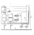
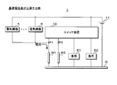
- FIG. It is a block diagram which shows the main part structure of the power supply system in Embodiment 1.
- FIG. It is a top view of the switch device. It is a circuit diagram of an adjustment circuit. It is a timing chart for explaining the operation of the adjustment circuit. It is explanatory drawing of the example that the reference potential difference rises.
- the switch device includes an output unit that outputs a plurality of voltages, a switch, a resistance to which one output voltage output by the output unit is input to one end, and the resistance.
- a switching circuit that switches the switch on or off according to the resistance voltage at the end, and the resistance voltage when all of the plurality of specific voltages included in the plurality of output voltages output by the output unit are equal to or higher than the output threshold value. It is provided with a lowering circuit for lowering.
- the switching circuit switches the switch on when the resistance voltage becomes a voltage equal to or higher than the resistance threshold, and the resistance voltage is a voltage lower than the resistance threshold.
- the switch is switched off, and the lowering circuit lowers the resistance voltage to a voltage lower than the resistance threshold when all of the plurality of specific voltages are equal to or higher than the output threshold.
- the switch when all the specific voltages are equal to or higher than the output threshold value, the switch is switched off.
- the output threshold value is less than the resistance threshold value.
- the output threshold is less than the resistance threshold. Therefore, when the output unit outputs an erroneous output voltage, it is possible to realize a decrease in the resistance voltage before the resistance voltage becomes a voltage equal to or higher than the resistance threshold value. As a result, it is possible to realize a decrease in the resistance voltage before the switch is switched on.
- the current flows in the order of the resistance member having the resistance component and the conductor, and the reference potential of the output unit is the first potential at one end on the upstream side of the resistance member.
- the switching circuit turns the switch on or off depending on the resistance voltage at which the reference potential is the second potential at a place different from one end on the upstream side of the resistance member.
- the lowering circuit lowers the resistance voltage when all of the plurality of specific voltages whose reference potential is the second potential is equal to or higher than the output threshold value.
- the output voltage (specific voltage) at which the reference potential is the second potential is the reference potential. Is higher by the potential difference than the output voltage (specific voltage) which is the first potential.
- the potential difference is equal to or greater than the output threshold value, all specific voltages are equal to or greater than the output threshold value regardless of the adjustment of the output voltage performed by the output unit.
- the switch device includes a second switch having one end connected to the other end of the resistor, and when the second switch is on, the current is the resistance, the second switch.
- the second switch and the conductor flow in this order, and the lowering circuit switches the second switch on when all of the plurality of specific voltages are equal to or higher than the output threshold value.
- the resistance voltage is lowered by switching the second switch on.
- the output voltage output by the output unit to one end of the resistor is one of the plurality of specific voltages.
- the output voltage output to one end of the resistor is used as one specific voltage.
- the output voltage output by the output unit to one end of the resistor is different from the plurality of specific voltages.
- the switch device includes a first substrate and a second substrate different from the first substrate, the output unit is arranged on the first substrate, and the second substrate has the output unit.
- the switch, resistor, switching circuit and lowering circuit are arranged.
- the output unit is arranged on the first substrate.
- the switch, resistor, switching circuit and lowering circuit are arranged on the second board.
- FIG. 1 is a block diagram showing a main configuration of the power supply system 1 according to the first embodiment.
- the power supply system 1 is mounted on the vehicle.
- the power supply system 1 includes a switch device 10, a DC power supply 11, two loads E1 and E2, and a conductor G.
- the DC power supply 11 is, for example, a battery.
- the conductor G is, for example, the body of a vehicle.
- the switch device 10 has two main switches F1 and F2.
- the main switch Fi is an N-channel type FET (Field Effect Transistor). When the main switch Fi is on, the resistance between the drain and source is small enough. Therefore, it is possible for a current to flow through the drain and source of the main switch Fi. When the main switch Fi is off, the resistance between the drain and source is large enough. Therefore, no current flows through the drain and source of the main switch Fi.
- the positive electrode of the DC power supply 11 is connected to the drain of the main switch Fi.
- the source of the main switch Fi is connected to one end of the load Ei.
- the negative electrode of the DC power supply 11 and the other ends of the loads E1 and E2 are connected to the conductor G. Grounding is achieved by connecting to the conductor G.
- the switch device 10 is separately connected to one end of the first conductor W1 and the second conductor W2.
- the other ends of the first conductor W1 and the second conductor W2 are connected to the conductor G.
- the positions of the conductors G to which the first conductor W1 and the second conductor W2 are connected are different from each other.
- the main switch Fi When the main switch Fi is switched on, the flow flows from the positive electrode of the DC power supply 11 in the order of the main switch Fi and the load Ei. As a result, power is supplied to the load Ei.
- the main switch Fi When the main switch Fi is switched off, the power supply to the load Ei is stopped.
- the load Ei is an electrical device. When power is supplied to the load Ei, the load Ei operates. When the power supply to the load Ei is stopped, the load Ei stops operating.
- the switch device 10 controls the operation of the load Ei by switching the main switch Fi on or off.
- the switch device 10 has to switch both the two main switches F1 and F2 on.
- the load E1 is a high beam light that illuminates the front of the vehicle.
- the load E2 is a low beam light that illuminates the lower front side of the vehicle.
- the switch device 10 includes a controller 20, a microcomputer (hereinafter referred to as a microcomputer) 21, and a regulator 22.
- the controller 20 has an adjustment circuit 30, two main switches F1 and F2, and two drive circuits H1 and H2.
- the gate of the main switch Fi is connected to the drive circuit Hi.
- the drive circuit Hi is separately connected to the microcomputer 21 via the adjustment circuit 30.
- the drive circuit Hi and the adjustment circuit 30 are connected to one end of the second conductor W2. As described above, the other end of the second conductor W2 is connected to the conductor G.
- the microcomputer 21 is further connected to the regulator 22 and one end of the first conductor W1. As described above, the other end of the first conductor W1 is connected to the conductor G.
- the regulator 22 is further connected to the drain of the main switch Fi and one end of the first conductor W1.
- the potential at one end of the first conductor W1 is referred to as the first potential P1.
- the potential at one end of the second conductor W2 is referred to as the second potential P2.
- the voltage of the positive electrode of the DC power supply 11 is referred to as a power supply voltage.
- the current flows from the positive electrode of the DC power supply 11 in the order of the regulator 22, the first conductor W1, and the conductor G.
- the regulator 22 steps down the power supply voltage whose reference potential is the first potential P1 to a constant voltage, and applies the stepped-down voltage to the microcomputer 21.
- the current flows from the positive electrode of the DC power supply 11 in the order of the regulator 22, the microcomputer 21, the first conductor W1, and the conductor G.
- electric power is supplied to the microcomputer 21. Since the current flows in the order of one end and the other end of the first conductor W1, the first potential P1 is the potential of one end on the upstream side of the first conductor W1.
- the microcomputer 21 outputs the output voltage for the drive circuit Hi. Therefore, the microcomputer 21 outputs two output voltages.
- the microcomputer 21 functions as an output unit.
- the microcomputer 21 adjusts the output voltage for the drive circuit Hi whose reference potential is the first potential P1 to a high level voltage or a low level voltage.
- the high level voltage and low level voltage are constant.
- the high level voltage is higher than the low level voltage.
- the low level voltage is zero V.
- the high level voltage is, for example, 5V.
- the adjustment circuit 30 adjusts the input voltage input to the drive circuit Hi based on the output voltage for the drive circuit Hi.
- the drive circuit Hi switches the main switch Fi on when the input voltage whose reference potential is the second potential P2 is equal to or higher than the input threshold value.
- the drive circuit Hi switches the main switch Fi to off when the input voltage at which the reference potential is the second potential P2 is less than the input threshold value.
- the input threshold value is a constant value and exceeds zero V.
- the drive circuit Hi functions as a switching circuit.
- the main switch Fi when the voltage of the gate whose reference potential is the potential of the source is a constant voltage or more, the main switch Fi is on. In the main switch Fi, when the voltage of the gate whose reference potential is the potential of the source is less than a constant voltage, the main switch Fi is off.
- the drive circuit Hi raises the voltage of the gate whose reference potential is the second potential P2.
- the voltage of the gate whose reference potential is the potential of the source becomes a voltage equal to or higher than a certain voltage.
- the main switch Fi is switched on.
- the drive circuit Hi lowers the voltage of the gate whose reference potential is the second potential P2.
- the main switch Fi the voltage of the gate whose reference potential is the potential of the source becomes a voltage less than a constant voltage.
- the main switch Fi is switched off.
- the drive circuit Hi switches the main switch Fi on or off by adjusting the voltage of the gate whose reference potential is the second potential P2.
- the adjustment circuit 30 compares the output voltage of the microcomputer 21 whose reference potential is the second potential P2 with the output threshold value.
- the output threshold is a constant value and exceeds zero V.
- the output threshold is less than or equal to the input threshold.
- the adjustment circuit 30 sets the input voltage of the drive circuit Hi to the output voltage for the drive circuit Hi whose reference potential is the second potential P2. Adjust to.
- the adjustment circuit 30 reduces the input voltages of the two drive circuits H1 and H2 to zero V.
- the two output voltages output by the microcomputer 21 correspond to two specific voltages.
- Each of the first conductor W1 and the second conductor W2 is a resistance member having a resistance component. Therefore, in the first conductor W1, when a current flows from one end on the microcomputer 21 side toward the conductor G, the first potential P1 rises with respect to the potential of the conductor G. The increase width increases as the current value of the current flowing through the first conductor W1 increases. Similarly, in the second conductor W2, when a current flows from one end on the adjustment circuit 30 side toward the conductor G, the second potential P2 rises with respect to the potential of the conductor G. The increase width increases as the current value of the current flowing through the second conductor W2 increases.
- the potential difference obtained by subtracting the second potential from the first potential will be referred to as a reference potential difference.
- the reference potential difference exceeds zero V
- the output voltage for the drive circuit Hi whose reference potential is the second potential P2 is only the reference potential difference from the output voltage for the drive circuit Hi whose reference potential is the first potential P1. high.
- the output threshold is less than or equal to the input threshold.
- the high level voltage is above the input threshold.
- the low level voltage is zero V and is below the output threshold.
- the microcomputer 21 does not adjust both of the two output voltages whose reference potential is the first potential P1 to the high level voltage. Therefore, the adjustment circuit 30 adjusts the input voltage of the drive circuit Hi to the output voltage for the drive circuit Hi whose reference potential is the second potential P2.
- the drive circuit Hi switches the main switch Fi on.
- the drive circuit Hi switches the main switch Fi to off.
- the microcomputer 21 changes the output voltage for the drive circuit Hi whose reference potential is the first potential P1 to a high level voltage or a low level voltage. By adjusting, the main switch Fi is switched on or off.
- the operation of the switch device 10 when the reference potential difference is equal to or greater than the output threshold value will be described.
- the output voltage for the drive circuit Hi whose reference potential is the first potential P1 is adjusted to the high level voltage
- the output voltage for the drive circuit Hi whose reference potential is the second potential P2 is equal to or higher than the output threshold value.
- the output voltage for the drive circuit Hi whose reference potential is the first potential P1 is adjusted to the low level voltage
- the output voltage for the drive circuit Hi whose reference potential is the second potential P2 is equal to or higher than the output threshold value.
- both of the two output voltages output by the microcomputer 21 are equal to or greater than the output threshold value.
- the adjustment circuit 30 reduces the input voltages of the two drive circuits H1 and H2 to zero V.
- the input threshold is above zero V. Therefore, when the adjustment circuit 30 reduces the input voltage of the two drive circuits H1 and H2 to zero V, the drive circuits H1 and H2 each switch the main switches F1 and F2 off.
- the adjustment circuit 30 reduces the input voltages of the two drive circuits H1 and H2 to zero V. As a result, each of the drive circuits H1 and H2 switches the main switches F1 and F2 off.
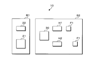
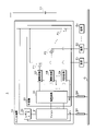
- FIG. 2 is a plan view of the switch device 10.
- the switch device 10 further includes a first substrate B1 and a second substrate B2.
- the second substrate B2 is different from the first substrate B1.
- a microcomputer 21 and a regulator 22 are arranged on the first substrate B1.
- the microcomputer 21 is, for example, an integrated circuit chip.
- the adjustment circuit 30, two main switches F1 and F2, and two drive circuits H1 and H2 are arranged on the second substrate B2. Specifically, one or a plurality of circuit elements constituting the circuit are arranged for each of the adjustment circuit 30 and the drive circuits H1 and H2. Therefore, the controller 20 is realized on the second substrate B2.
- the first substrate B1 and the conductor G are connected by the first conductor W1.
- the second substrate B2 and the conductor G are connected by the second conductor W2.
- microcomputer 21, the regulator 22, the adjustment circuit 30, the two main switches F1 and F2, and the two drive circuits H1 and H2 may be arranged on one board.
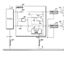
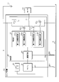
- FIG. 3 is a circuit diagram of the adjustment circuit 30.
- the adjustment circuit 30 has an AND circuit 40, two switch circuits J1 and J2, and two connection resistors R1 and R2.
- the AND circuit 40 has two input ends and an output end.
- the connection resistor Ri is connected between the microcomputer 21 and the drive circuit Hi.
- the connection node between the microcomputer 21 and the connection resistor Ri is connected to the input end of the AND circuit 40. Therefore, the two input ends of the AND circuit 40 are separately connected to the microcomputer 21.
- the switch circuit Ji is connected to a connection node between the drive circuit Hi and the connection resistor Ri, an output end of the AND circuit 40, and one end of the second conductor W2.
- the switch circuit Ji has a sub switch 50 and circuit resistors 51 and 52.
- the configuration of the switch circuit J1 is shown as a representative.
- the sub switch 50 is an NPN type bipolar transistor. When the subswitch 50 is on, the resistance between the collector and the emitter is small enough. Therefore, it is possible for a current to flow through the collector and the emitter. When the subswitch 50 is off, the resistance value between the collector and the emitter is large enough. Therefore, no current flows through the collector and the emitter.
- the collector of the sub switch 50 is connected to one end of the drive circuit Hi side of the connection resistor Ri.
- the sub switch 50 functions as a second switch.
- the emitter of the subswitch 50 is connected to one end of the second conductor W2.
- a circuit resistor 51 is connected between the base and the emitter of the subswitch 50.
- One end of the circuit resistor 52 is connected to the base of the sub switch 50.
- the other end of the circuit resistor 52 is connected to the output end of the AND circuit 40.
- the output voltage for the drive circuit Hi output by the microcomputer 21 is input to one end of the connection resistor Ri.
- the voltage at one end of the drive circuit Hi side of the connection resistor Ri is input to the drive circuit Hi as an input voltage.
- the input voltage and the input threshold value correspond to the resistance voltage and the resistance threshold value, respectively.
- the drive circuit Hi switches the main switch Fi on or off according to the input voltage.
- the sub switch 50 of the switch circuit Ji when the base voltage whose reference potential is the potential of the emitter is less than a constant voltage, the sub switch 50 is off.
- the constant voltage is a positive value.
- the output voltage for the drive circuit Hi whose reference potential is the second potential P2 is input to the drive circuit Hi as an input voltage.
- the drive circuit Hi monitors the input voltage whose reference potential is the second potential P2.
- the subswitch 50 of the switch circuit Ji when the base voltage whose reference potential is the potential of the emitter is a constant voltage or more, the subswitch 50 is on. When the subswitch 50 is on, the input voltage whose reference potential is the second potential P2 is lowered to zero V. When the input voltage is zero V, the input voltage is less than the input threshold. Therefore, the drive circuit Hi switches the main switch Fi to off. When the output voltage for the drive circuit Hi whose reference potential is the second potential exceeds zero V, when the sub switch 50 is on, the current flows in the order of the connection resistance Ri, the sub switch 50, and the conductor G. ..
- the AND circuit 40 compares the output voltage for the drive circuit Hi whose reference potential is the second potential P2 with the output threshold value. When at least one of the two output voltages is less than the output threshold value, the AND circuit 40 adjusts the voltage at the output end where the reference potential is the second potential P2 to zero V. In this case, in the switch circuit Ji, no current flows through the circuit resistor 51. Therefore, for the subswitch 50, the base voltage, which is the potential of the emitter, is zero V, which is less than a constant voltage. As a result, the sub switch 50 is off.
- the AND circuit 40 adjusts the voltage at the output end whose reference potential is the second potential P2 to a positive predetermined voltage.
- the current flows in the order of the circuit resistors 52, 51, the second conductor W2, and the conductor G.
- a voltage drop occurs in the circuit resistance 51, so that the base voltage, which is the potential of the emitter, of the subswitch 50 is equal to or higher than a constant voltage.
- the sub switch 50 is on.
- the AND circuit 40 When the AND circuit 40 switches on the sub-switch 50 of the switch circuits J1 and J2, the input voltage of the drive circuits H1 and H2 whose reference potential is the second potential P2 is lowered to zero V.
- the AND circuit 40 functions as a drop circuit.
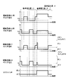
- FIG. 4 is a timing chart for explaining the operation of the adjustment circuit 30.
- FIG. 4 shows a transition of the output voltage for the drive circuit Hi, a transition of the input voltage of the drive circuit Hi, and a transition of the state of the subswitch 50 of the drive circuits H1 and H2.
- the state of the subswitch 50 of the drive circuits H1 and H2 is always the same.
- the output threshold value and the input threshold value are represented by Vs and Vt, respectively.
- FIG. 4 shows two output voltages and two input voltages whose reference potential is the second potential P2. As described above, the output threshold value Vs is equal to or less than the input threshold value Vt.
- the operation when the reference potential difference is small that is, when the reference potential difference is zero V or more and less than the output threshold value Vs will be described.
- the reference potential difference when the reference potential difference is small, when the output voltage for the drive circuit Hi whose reference potential is the first potential P1 is a high level voltage, for the drive circuit Hi whose reference potential is the second potential P2.
- the output voltage of is equal to or higher than the output threshold Vs.
- the microcomputer 21 does not adjust both of the two output voltages whose reference potential is the first potential P1 to the high level voltage. Therefore, when the reference potential difference is small, the subswitch 50 of the switch circuits J1 and J2 is off.
- the output voltage for the drive circuit Hi whose reference potential is the second potential P2 is input to the drive circuit Hi as an input voltage. Therefore, when the microcomputer 21 adjusts the output voltage for the drive circuit Hi whose reference potential is the first potential P1 to a high level voltage, the input voltage of the drive circuit Hi becomes a voltage equal to or higher than the input threshold voltage Vt. As described above, the high level voltage is equal to or higher than the input threshold value Vt. When the input voltage of the drive circuit Hi becomes a voltage equal to or higher than the input threshold value Vt, the drive circuit Hi switches the main switch Fi to ON.
- the input voltage of the drive circuit Hi becomes a voltage less than the input threshold voltage Vt.
- the low level voltage is less than the input threshold Vt.
- the adjustment circuit 30 when the subswitch 50 of each of the switch circuits J1 and J2 is switched on, the input voltage of the drive circuits H1 and H2 whose reference potential is the second potential P2 is lowered to zero V. As a result, each of the drive circuits H1 and H2 switches the main switches F1 and F2 off. The two main switches F1 and F2 are kept off while the reference potential difference is large.
- the subswitch 50s of the switch circuits J1 and J2 are switched off.
- the output voltage for the drive circuit Hi whose reference potential is the second potential P2 is input to the drive circuit Hi as an input voltage.
- the microcomputer 21 switches the main switch Fi on or off by adjusting the output voltage for the drive circuit Hi whose reference potential is the first potential P1.
- the output threshold value Vs is preferably less than the input threshold value Vt. It is assumed that the period from when both of the two output voltages whose reference potential is the second potential P2 becomes the voltage equal to or higher than the output threshold Vs until the subswitch 50 of the switch circuits J1 and J2 is switched off is sufficiently short. do. In this case, after both of the two output voltages having the reference potential of the second potential P2 become voltages equal to or higher than the output threshold Vs, all the input voltages having the reference potential of the second potential P2 are equal to or higher than the input threshold Vt. By the time the voltage reaches the voltage of, all the input voltages whose reference potential is the second potential P2 are lowered to zero V.
- the drive circuit Hi keeps the main switch Fi off. As a result, it is possible to realize a decrease in the input voltage of the drive circuits H1 and H2 before all the main switches F1 and F2 are switched on.
- FIG. 5 is an explanatory diagram of an example in which the reference potential difference increases.
- the power supply system 1 has a plurality of electrical devices K. Each electric device K is connected between the positive electrode of the DC power supply 11 and one end of the first conductor W1.
- the electric device K When the electric device K is activated, the current flows from the positive electrode of the DC power supply 11 in the order of the electric device K, the first conductor W1, and the conductor G. As a result, electric power is supplied to the electric device K.
- the electric device K is stopped, no current flows through the electric device K.
- the first conductor W1 has a resistance component. Therefore, when a current flows through the first conductor W1, a voltage drop occurs in the first conductor W1. As a result, the first potential P1 rises with respect to the potential of the conductor G.
- the reference potential difference rises.
- the larger the current value of the current flowing through the first conductor W1 the wider the width of the voltage drop.
- the larger the voltage drop width the larger the rise width of the reference potential difference. Therefore, the larger the current value of the current flowing through the first conductor W1, the larger the increase width of the reference potential difference.
- the reference potential difference may become a value equal to or larger than the output threshold value.
- the reference potential difference increases. For example, when disturbance noise is applied to one end of the first conductor W1, a current may flow through the first conductor W1. As described above, when a current flows through the first conductor W1, the reference potential difference increases.
- the number of main switches included in the switch device 10 in the first embodiment is two. However, the number of main switches included in the switch device 10 is not limited to two.
- the difference between the second embodiment and the first embodiment will be described.
- Other configurations other than the configurations described later are common to the first embodiment. Therefore, the same reference reference numerals as those in the first embodiment are assigned to the components common to the first embodiment, and the description of the components will be omitted.
- FIG. 6 is a block diagram showing a main configuration of the power supply system 1 according to the second embodiment.
- the power supply system 1 in the second embodiment includes a switch device 10, a DC power supply 11, and a conductor G, as in the first embodiment.
- the power supply system 1 in the second embodiment further includes n loads E1, E2, ..., En.
- n is an integer of 3 or more.
- the integer i may be any of 1, 2, ..., N.
- the switch device 10 has n main switches F1, F2, ..., Fn.
- the main switch Fi is configured in the same manner as in the first embodiment.
- the main switch Fi and the load Ei are connected in the same manner as in the first embodiment.
- the positions of the conductors G to which the first conductor W1 and the second conductor W2 are connected are different from each other.
- the load Ei operates in the same manner as in the first embodiment. Similar to the first embodiment, the switch device 10 controls the power supply to the load Ei by switching the main switch Fi on or off. There is no situation where the loads E1, E2, ..., En must be operated at the same time. Therefore, there is no situation in which the switch device 10 has to switch on all of the n main switches F1, F2, ..., Fn.
- the controller 20 in the second embodiment has an adjustment circuit 30 as in the first embodiment.
- the controller 20 in the second embodiment further has n main switches F1, F2, ..., Fn and n drive circuits H1, H2, ..., Hn.
- the main switch Fi and the drive circuit Hi are connected in the same manner as in the first embodiment.
- the microcomputer 21 outputs the output voltage for the drive circuit Hi as in the first embodiment. Therefore, the microcomputer 21 outputs n output voltages.
- the adjustment circuit 30 adjusts the input voltage input to the drive circuit Hi based on the output voltage for the drive circuit Hi.
- the drive circuit Hi switches the main switch Fi on or off as in the first embodiment.
- the adjustment circuit 30 compares the output voltage of the microcomputer 21 whose reference potential is the second potential P2 with the output threshold value, as in the first embodiment. When at least one of the n output voltages output by the microcomputer 21 is less than the output threshold value, the adjustment circuit 30 outputs the input voltage of the drive circuit Hi for the drive circuit Hi whose reference potential is the second potential P2. Adjust to voltage. When all of the n output voltages output by the microcomputer 21 are equal to or greater than the output threshold value, the adjusting circuit 30 reduces the input voltages of the n drive circuits H1, H2, ..., Hn to zero V. The n output voltages output by the microcomputer 21 correspond to n specific voltages.
- the microcomputer 21 does not adjust all the output voltages of the n drive circuits H1, H2, ..., Hn whose reference potential is the first potential P1 to a high level voltage. Therefore, when the reference potential difference is less than the output threshold value, the adjustment circuit 30 adjusts the input voltage of the drive circuit Hi to the output voltage for the drive circuit Hi whose reference potential is the second potential P2. Therefore, the microcomputer 21 switches the main switch Fi on or off by adjusting the output voltage for the drive circuit Hi whose reference potential is the first potential P1 to a high level voltage or a low level voltage.
- the adjustment circuit 30 reduces the input voltages of the n drive circuits H1, H2, ..., Hn to zero V. As a result, each of the n drive circuits H1, H2, ..., Hn switches the main switches F1, F2, ..., Fn off. While the reference potential difference is equal to or greater than the output threshold value, each of the n drive circuits H1, H2, ..., Hn is fixed to off the main switches F1, F2, ..., Fn.
- the adjustment circuit 30 sets the input voltages of the n drive circuits H1, H2, ..., Hn to zero V. Adjust to. As a result, the drive circuits H1, H2, ..., Hn each switch the main switches F1, F2, ..., Fn off.
- the adjustment circuit 30, n main switches F1, F2, ..., Fn and n drive circuits H1, H2, ..., Hn are arranged on the second substrate B2.
- a microcomputer 21, a regulator 22, an adjustment circuit 30, n main switches F1, F2, ..., Fn and n drive circuits H1, H2, ..., Hn are arranged on one board. You may.
- FIG. 7 is a circuit diagram of the adjustment circuit 30.
- the adjustment circuit 30 has an AND circuit 40 as in the first embodiment.
- the adjusting circuit 30 further has n switch circuits J1, J2, ..., Jn and n connection resistors R1, R2, ..., Rn.
- the AND circuit 40 has n input ends.
- the switch circuit Ji is configured in the same manner as in the first embodiment, and has a sub switch 50 and circuit resistors 51 and 52.
- the connection resistor Ri and the switch circuit Ji are connected in the same manner as in the first embodiment.
- the switch circuit Ji operates in the same manner as in the first embodiment.
- the AND circuit 40 compares the output voltage for the drive circuit Hi whose reference potential is the second potential P2 with the output threshold value.
- the AND circuit 40 adjusts the voltage at the output end where the reference potential is the second potential P2 to zero V when at least one of the n output voltages is less than the output threshold.
- the subswitch 50 of the switch circuits J1, J2, ..., Jn is off.
- the output voltage for the drive circuit Hi whose reference potential is the second potential P2 is input to the drive circuit Hi as an input voltage.
- the microcomputer 21 switches the main switch Fi on or off by adjusting the output voltage for the drive circuit Hi whose reference potential is the first potential P1 to a high level voltage or a low level voltage.
- the AND circuit 40 adjusts the voltage at the output end whose reference potential is the second potential P2 to a positive predetermined voltage.
- the subswitch 50 of the switch circuits J1, J2, ..., Jn is on.
- the n drive circuits H1 whose reference potential is the second potential P2. , H2, ..., The input voltage of Hn drops to zero V.
- the input threshold is above zero V.
- each of the drive circuits H1, H2, ..., Hn switches the main switches F1, F2, ..., Fn to off. While the reference potential difference is equal to or greater than the output threshold value, the n main switches F1, F2, ..., Fn are fixed to off.
- the output threshold value is preferably less than the input threshold value. In this case, it is possible to reduce the input voltage of the drive circuits H1, H2, ..., Hn before all the main switches F1, F2, ..., Fn are switched on.
- the number of output voltages monitored by the adjustment circuit 30 may be less than n.
- the number of output voltages monitored by the adjusting circuit 30 may be 2 or more.
- the adjustment circuit 30 may monitor the x output voltages whose reference potential is the second potential. ..
- x is an integer that is greater than or equal to 2 and less than or equal to n.
- the AND circuit 40 of the adjustment circuit 30 has x input ends. The AND circuit 40 is connected to one end of x connection resistors to which x output voltages are input among n connection resistors R1, R2, ..., Rn.
- the output voltage monitored by the adjusting circuit 30 corresponds to a specific voltage.
- the adjustment circuit 30 uses the input voltage of the drive circuit Hi for the drive circuit Hi whose reference potential is the second potential when at least one of the x output voltages whose reference potential is the second potential is less than the output threshold. Adjust to the output voltage of.
- the adjustment circuit 30 lowers the input voltages of n drive circuits H1, H2, ..., Hn to zero V when all of the x output voltages whose reference potential is the second potential are equal to or higher than the output threshold value. Let me.
- the load connected to the switch device 10 is not limited to the electric device in which the current flows in only one direction.
- the differences between the third embodiment and the first embodiment will be described.
- Other configurations other than the configurations described later are common to the first embodiment. Therefore, the same reference reference numerals as those in the first embodiment are assigned to the components common to the first embodiment, and the description of the components will be omitted.
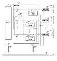
- FIG. 8 is a block diagram showing a main configuration of the power supply system 1 according to the third embodiment.
- the power supply system 1 in the third embodiment includes a switch device 10 and a DC power supply 11 as in the first embodiment.
- the power supply system 1 further includes a motor 12 as a load.
- the switch device 10 has four main switches F1u, F1d, F2u, and F2d.
- the configurations of the main switches F1u, F1d, F2u, and F2d are the same as the configurations of the main switch F1 in the first embodiment.
- the negative electrode of the DC power supply 11 is connected to the conductor G.
- the drains of the main switches F1u and F2u are connected to the positive electrode of the DC power supply 11.
- the sources of the main switches F1u and F2u are connected to the drains of the main switches F2d and F1d.
- the sources of the main switches F1d and F2d are connected to the conductor G.
- the motor 12 is separately connected to a connection node between the main switches F1u and F2d and a connection node between the main switches F2u and F1d.
- the switch device 10 is separately connected to one end of the first conductor W1 and the second conductor W2.
- the other ends of the first conductor W1 and the second conductor W2 are connected to the conductor G.
- the positions of the conductors G to which the first conductor W1 and the second conductor W2 are connected are different from each other.
- switch states A state in which the main switches F1u and F1d are on and the main switches F2u and F2d are off is described as a forward rotation state. A state in which the main switches F1u and F1d are off and the main switches F2u and F2d are on is described as a reverse rotation state. A state in which the main switches F1u and F2u are off and the main switches F1d and F2d are on is described as a discharge state. The state in which the main switches F1u, F1d, F2u, and F2d are off is described as an off state.
- the switch device 10 shifts the switch state to a forward rotation state, a reverse rotation state, a discharge state, or an off state by switching each of the main switches F1u, F1d, F2u, and F2d on or off.
- the switch device 10 shifts the switch state to the normal rotation state, the current flows from the positive electrode of the DC power supply 11 in the order of the main switch F1u, the motor 12, the main switch F1d, and the conductor G. At this time, the motor 12 rotates in the forward direction.
- the switch device 10 shifts the switch state to the reverse rotation state
- the current flows from the positive electrode of the DC power supply 11 in the order of the main switch F2u, the motor 12, the main switch F2d, and the conductor G. At this time, the motor 12 rotates in the reverse direction.
- the motor 12 has a columnar rotor that rotates around an axis. Positive rotation is, for example, clockwise rotation of the rotor. In this case, the counterclockwise rotation is the counterclockwise rotation of the rotor.
- the motor 12 has an inductor. Energy is stored in the inductor of the motor 12 while the current is flowing through the motor 12.
- the controller 20 in the third embodiment has an adjustment circuit 30 as in the first embodiment.
- the controller 20 in the third embodiment further includes a drive IC 31 and four main switches F1u, F1d, F2u, and F2d.
- the drive IC 31 has a first upper drive circuit H1u, a first lower drive circuit H1d, a second upper drive circuit H2u, and a second lower drive circuit H2d.
- the first upper drive circuit H1u, the first lower drive circuit H1d, the second upper drive circuit H2u, and the second lower drive circuit H2d are connected to the gates of the main switches F1u, F1d, F2u, and F2d, respectively.
- the first upper drive circuit H1u, the first lower drive circuit H1d, the second upper drive circuit H2u, and the second lower drive circuit H2d each have the same main switches F1u, F1d, and F2u as the drive circuit H1 in the first embodiment. , F2d is switched on or off.
- the drive IC 31 is connected to the adjustment circuit 30.
- the adjustment circuit 30 is connected to the microcomputer 21.
- the adjustment circuit 30 and the drive IC 31 are connected to one end of the second conductor W2.
- the microcomputer 21 outputs the first output voltage, the second output voltage, and the third output voltage. Therefore, the microcomputer 21 outputs three output voltages.
- the microcomputer 21 adjusts each of the first output voltage, the second output voltage, and the third output voltage whose reference potential is the first potential P1 to a high level voltage or a low level voltage.
- the adjustment circuit 30 adjusts the first input voltage input to the drive IC 31 based on the first output voltage whose reference potential is the second potential P2.
- the adjusting circuit 30 adjusts the second input voltage input to the drive IC 31 based on the second output voltage whose reference potential is the second potential P2.
- the adjusting circuit 30 adjusts the third input voltage input to the drive IC 31 based on the third output voltage whose reference potential is the second potential P2.
- the drive IC 31 shifts the switch state to a forward rotation state, a reverse rotation state, a discharge state, or an off state according to the first input voltage, the second input voltage, and the third input voltage whose reference potential is the second potential P2.
- FIG. 9 is a timing chart for explaining the operation of the drive IC 31.
- FIG. 9 shows the transition of the states of the main switches F1u, F1d, F2u, and F2d, and the transition of the first input voltage, the second input voltage, and the third input voltage. Time is shown on the horizontal axis of these transitions. Also in FIG. 9, the input threshold value is represented by Vt.
- the first upper drive circuit H1u and the first lower drive circuit H1d are the main switches, respectively. Switch F1u and F1d on. Further, the second upper drive circuit H2u and the second lower drive circuit H2d switch the main switches F2u and F2d off, respectively. As a result, the switch state transitions to the forward rotation state.
- the forward rotation of the motor 12 is instructed by adjusting the first input voltage to a voltage equal to or higher than the input threshold value Vt.
- the first upper drive circuit H1u and the first lower drive circuit H1d are the main switches, respectively. Switch F1u and F1d off. Further, the second upper drive circuit H2u and the second lower drive circuit H2d switch the main switches F2u and F2d on, respectively. As a result, the switch state transitions to the reverse rotation state. By adjusting the second input voltage to a voltage equal to or higher than the input threshold value Vt, the reverse rotation of the motor 12 is instructed.
- the first upper drive circuit H1u and the second upper drive circuit H2u are the main switches F1u, respectively.
- F2u is switched off.
- the first lower drive circuit H1d and the second lower drive circuit H2d switch the main switches F1d and F2d on, respectively.
- the switch state transitions to the discharge state. Discharge of the motor 12 is instructed by adjusting the third input voltage to a voltage equal to or higher than the input threshold value Vt.
- the first upper drive circuit H1u, the first lower drive circuit H1d, the second upper drive circuit H2u and the second lower drive Each of the circuits H2d switches the main switches F1u, F1d, F2u, and F2d off.
- the switch state transitions to the off state.
- the drive IC 31 shifts the switch state to the forward rotation state, the reverse rotation state, the discharge state, or the off state based on the first input voltage, the second input voltage, and the third input voltage.
- the adjustment circuit 30 shown in FIG. 8 compares each of the first output voltage, the second output voltage, and the third output voltage whose reference potential is the second potential P2 with the output threshold value. When at least one of the first output voltage, the second output voltage, and the third output voltage is less than the output threshold, the adjusting circuit 30 has a reference potential for each of the first input voltage, the second input voltage, and the third input voltage. The voltage is adjusted to the first output voltage, the second output voltage, and the third output voltage, which are the second potentials P2. The adjusting circuit 30 lowers each of the first input voltage, the second input voltage, and the third input voltage to zero V when all of the first output voltage, the second output voltage, and the third output voltage are equal to or higher than the output threshold. .. The first output voltage, the second output voltage, and the third output voltage correspond to three specific voltages.
- the output threshold value is equal to or less than the input threshold value.
- the high level voltage is above the input threshold.
- the low level voltage is zero V and is below the output threshold.
- the first output voltage whose reference potential is the first potential P1 is adjusted to the low level voltage
- the first output voltage whose reference potential is the second potential P2 is less than the output threshold value.
- the second output voltage whose reference potential is the first potential P1 is adjusted to the low level voltage
- the second output voltage whose reference potential is the second potential P2 is less than the output threshold.
- the third output voltage whose reference potential is the first potential P1 is adjusted to the low level voltage
- the third output voltage whose reference potential is the second potential P2 is less than the output threshold.
- the microcomputer 21 does not adjust all of the first output voltage, the second output voltage, and the third output voltage whose reference potential is the first potential P1 to the high level voltage. Specifically, the microcomputer 21 adjusts only one of the first output voltage, the second output voltage, and the third output voltage whose reference potential is the first potential P1 to the high level voltage. Therefore, the adjusting circuit 30 adjusts the first input voltage, the second input voltage, and the third input voltage to the first output voltage, the second output voltage, and the third output voltage whose reference potential is the second potential P2, respectively. ..
- the drive IC 31 shifts the switch state to the normal rotation state.
- the drive IC 31 shifts the switch state to the reverse rotation state.
- the drive IC 31 shifts the switch state to the discharge state.
- the drive IC 31 shifts the switch state to the off state.
- the microcomputer 21 sets the first output voltage, the second output voltage, and the third output voltage whose reference potential is the first potential P1, respectively.
- the switch state is changed to a forward rotation state, a reverse rotation state, a discharge state, or an off state.
- the microcomputer 21 sets the switch state in order to prevent both ends of the DC power supply 11 from being short-circuited. Transition to the off state. Next, the microcomputer 21 shifts the switch state to the discharge state. As a result, the energy stored in the inductor of the motor 12 is released. After that, the microcomputer 21 shifts the switch state to the off state again. Finally, the microcomputer 21 shifts the switch state to the reverse rotation state.
- the microcomputer 21 When the switch state is in the reverse rotation state and the switch state is changed to the forward rotation state, the microcomputer 21 similarly shifts the switch state to the off state, the discharge state, the off state and the forward rotation state.
- the switch device 10 when the reference potential difference is equal to or greater than the output threshold value will be described.
- the first output voltage, the second output voltage, and the third output voltage are equal to or greater than the output threshold value and do not drop to a voltage lower than the output threshold value. Therefore, the adjustment circuit 30 lowers the first input voltage, the second input voltage, and the third input voltage to zero V. As described in the description of the first embodiment, the input threshold value exceeds zero V. Therefore, when the adjusting circuit 30 reduces the first input voltage, the second input voltage, and the third input voltage to zero V, the drive IC 31 shifts the switch state to the off state.
- the adjustment circuit 30 causes the first input voltage, the second input voltage, and the third output voltage. 3 Reduce the input voltage to zero V. As a result, the drive IC 31 shifts the switch state to the off state.
- the adjustment circuit 30, the four main switches F1u, F1d, F2u, F2d and the drive IC 31 are arranged on the second substrate B2.
- a microcomputer 21, a regulator 22, an adjustment circuit 30, four main switches F1u, F1d, F2u, F2d, and a drive IC 31 may be arranged on one board.
- the adjustment circuit 30 in the third embodiment is configured in the same manner as the adjustment circuit 30 in the second embodiment when the integer n is 3.
- the microcomputer 21 outputs each of the first output voltage, the second output voltage, and the third output voltage to one end of the connection resistors R1, R2, and R3.
- the other ends of the three connection resistors R1, R2, and R3 are separately connected to the drive IC 31.
- the drive IC 31 changes the switch state to the forward rotation state, the reverse rotation state, and the discharge state according to the first input voltage, the second input voltage, and the third input voltage input from the other ends of the connection resistors R1, R2, and R3. Or transition to the off state.
- FIG. 10 is a timing chart for explaining the operation of the adjustment circuit 30.
- FIG. 10 shows changes in the first output voltage, the second output voltage, the third output voltage, the first input voltage, the second input voltage, and the third input voltage whose reference potential is the second potential P2.
- FIG. 10 further shows the transition of the state of the subswitch 50 of the switch circuits J1, J2, J3. The states of the three subswitches 50 are always the same.
- the output threshold value and the input threshold value are represented by Vs and Vt, respectively.
- the AND circuit 40 keeps the subswitch 50 of the switch circuits J1, J2, J3 off.
- the subswitch 50 of the switch circuits J1, J2 and J3 is off, the first output voltage, the second output voltage and the third output voltage whose reference potential is the second potential P2 are the first input voltage and the second, respectively. It is input to the drive IC 31 as an input voltage and a third input voltage. Therefore, as described above, the microcomputer 21 changes the switch state to the forward rotation state and the reverse rotation state by adjusting the first output voltage, the second output voltage, and the third output voltage whose reference potential is the first potential P1. , Discharge state or off state.
- the reference potential difference becomes a value equal to or higher than the output threshold value Vs.
- the reference potential difference becomes large, all of the first output voltage, the second output voltage, and the third output voltage whose reference potential is the second potential P2 are equal to or higher than the output threshold value Vs.
- the AND circuit 40 switches the subswitch 50 of each of the switch circuits J1, J2, and J3 on.
- the drive IC 31 shifts the switch state to the off state.
- the switch state is fixed to the off state while the reference potential difference is large.
- the AND circuit 40 switches off the subswitch 50 of each of the switch circuits J1, J2, J3.
- the first output voltage, the second output voltage, and the third output voltage, each of which has a reference potential of the second potential P2 are the second. It is input to the drive IC 31 as 1 input voltage, 2nd input voltage and 3rd input voltage.
- the microcomputer 21 changes the switch state to a forward rotation state, a reverse rotation state, a discharge state, or an off state by adjusting the first output voltage, the second output voltage, and the third output voltage whose reference potential is the first potential P1. Make a transition.
- the adjustment circuit 30 causes the microcomputer 21 to make an erroneous output voltage when all of the first output voltage, the second output voltage, and the third output voltage output by the microcomputer 21 are equal to or higher than the output threshold. Assuming that it is output, the first input voltage, the second input voltage, and the third input voltage are lowered to zero V. As a result, the switch state transitions to the off state. As a result, the main switches F1u, F1d, F2u, and F2d for stopping the operation of the motor 12 are switched.
- the switch device 10 in the third embodiment similarly exhibits the effect of the switch device 10 in the first embodiment.
- the output threshold value is preferably less than the input threshold value. In this case, it is possible to reduce the first input voltage, the second input voltage, and the third input voltage before all the main switches F1u, F1d, F2u, and F2d are switched on.
- the adjusting circuit 30 sets only the first input voltage and the second input voltage to zero V. May be reduced to.
- the drive IC 31 shifts the switch state to the discharge state.
- the microcomputer 21 adjusts only one of the first output voltage, the second output voltage, and the third output voltage whose reference potential is the first potential P1 to the high level voltage. Therefore, when the reference potential difference is less than the output threshold value, the microcomputer 21 adjusts two of the first output voltage, the second output voltage, and the third output voltage whose reference potential is the second potential P2 to the high level voltage. There is no such thing. Therefore, the output voltage monitored by the adjusting circuit 30 may be two of the first output voltage, the second output voltage, and the third output voltage.
- the AND circuit 40 of the adjustment circuit 30 has two input ends. Two of the first output voltage, the second output voltage and the third output voltage are input to the AND circuit 40. When at least one of the two output voltages having the reference potential of the second potential is less than the output threshold value, the adjusting circuit 30 determines that the first input voltage, the second input voltage, and the third input voltage have a second reference potential. The potentials are adjusted to the first output voltage, the second output voltage, and the third output voltage. The adjusting circuit 30 lowers the first input voltage, the second input voltage, and the third input voltage to zero V when both of the two output voltages having the reference potential of the second potential are equal to or higher than the output threshold.
- the adjustment circuit 30 monitors the output voltage for the drive circuit Hi.
- the output voltage monitored by the adjustment circuit 30 is not limited to the output voltage for the drive circuit Hi.
- the differences between the fourth embodiment and the first embodiment will be described.
- Other configurations other than the configurations described later are common to the first embodiment. Therefore, the same reference reference numerals as those in the first embodiment are assigned to the components common to the first embodiment, and the description of the components will be omitted.
- FIG. 11 is a block diagram showing a main configuration of the power supply system 1 according to the fourth embodiment.
- the power supply system 1 in the fourth embodiment includes other components other than the load E2 among the components included in the power supply system 1 in the first embodiment.
- the switch device 10 in the fourth embodiment has a main switch F1 as in the first embodiment.
- the switch device 10 in the fourth embodiment controls the operation of the load E1 by switching the main switch F1 on or off.
- the switch device 10 in the fourth embodiment has a controller 20, a microcomputer 21, and a regulator 22 as in the first embodiment.
- the controller 20 has an adjustment circuit 30, a main switch F1 and a drive circuit H1 as in the first embodiment.
- the microcomputer 21 outputs a plurality of output voltages.
- the microcomputer 21 adjusts each of the plurality of output voltages whose reference potential is the first potential P1 to a high level voltage or a low level voltage.
- the plurality of output voltages output by the microcomputer 21 include an output voltage for the drive circuit H1 and a plurality of output voltages for monitoring.
- the output voltage for monitoring will be referred to as a specific voltage.
- the adjusting circuit 30 adjusts the input voltage input to the driving circuit H1 based on the output voltage for the driving circuit H1.
- the drive circuit H1 switches the main switch F1 on when the input voltage whose reference potential is the second potential P2 is equal to or higher than the input threshold value.
- the drive circuit H1 switches the main switch F1 off when the input voltage at which the reference potential is the second potential P2 is less than the input threshold value.
- the adjustment circuit 30 compares each of the plurality of specific voltages whose reference potential is the second potential P2 with the output threshold value. When at least one of the plurality of specific voltages output by the microcomputer 21 is less than the output threshold value, the adjustment circuit 30 sets the input voltage of the drive circuit H1 as the output voltage for the drive circuit H1 whose reference potential is the second potential P2. Adjust to. The adjustment circuit 30 reduces the input voltage of the drive circuit H1 to zero V when all the specific voltages output by the microcomputer 21 are equal to or higher than the output threshold value.
- the output threshold value is equal to or less than the input threshold value.
- the high level voltage is above the input threshold.
- the low level voltage is zero V and is below the output threshold.
- the microcomputer 21 does not adjust all of the plurality of specific voltages whose reference potential is the first potential P1 to the high level voltage. Therefore, the adjustment circuit 30 adjusts the input voltage of the drive circuit H1 to the output voltage for the drive circuit H1 whose reference potential is the second potential P2.
- the drive circuit H1 switches the main switch F1 on.
- the drive circuit H1 switches the main switch F1 off.
- the microcomputer 21 changes the output voltage for the drive circuit H1 whose reference potential is the first potential P1 to a high level voltage or a low level voltage. By adjusting, the main switch F1 is switched on or off.
- the operation of the switch device 10 when the reference potential difference is equal to or greater than the output threshold value will be described.
- the reference potential difference is equal to or greater than the output threshold value
- all of the plurality of specific voltages whose reference potential is the second potential P2 are equal to or greater than the output threshold value.
- the adjustment circuit 30 reduces the input voltage of the drive circuit H1 to zero V.
- the input threshold is above zero V. Therefore, when the adjustment circuit 30 reduces the input voltage of the drive circuit H1 to zero V, the drive circuit H1 switches the main switch F1 off.
- the adjustment circuit 30 reduces the input voltage of the drive circuit H1 to zero V. As a result, the drive circuit H1 switches the main switch F1 off.
- the number of specific voltages is 2
- an example of the first specific voltage is a voltage that instructs the switch to be turned on or off.
- the second specific voltage is, for example, a voltage instructing the cutoff of dark current. By switching the first specific voltage to a high level voltage, the switch is instructed to turn on. By switching the second specific voltage to the high level voltage, the cutoff of the dark current is instructed. Both the first specific voltage and the second specific voltage are not switched to the high level voltage.
- the adjustment circuit 30, the main switch F1 and the drive circuit H1 are arranged on the second substrate B2.
- the microcomputer 21, the regulator 22, the adjustment circuit 30, the main switch F1 and the drive circuit H1 may be arranged on one board.
- FIG. 12 is a circuit diagram of the adjustment circuit 30.
- the adjustment circuit 30 has an AND circuit 40, a switch circuit J1 and a connection resistor R1 as in the first embodiment.
- the AND circuit 40 has a plurality of input ends. A plurality of specific voltages output by the microcomputer 21 are input to the AND circuit 40 separately. The output voltage for the drive circuit H1 output by the microcomputer 21 is output to one end of the connection resistor R1.
- the switch circuit J1 operates in the same manner as in the first embodiment.
- the AND circuit 40 compares each of the plurality of specific voltages whose reference potential is the second potential P2 with the output threshold value.
- the AND circuit 40 adjusts the voltage at the output end where the reference potential is the second potential P2 to zero V when at least one of the plurality of specific voltages is less than the output threshold value. In this case, the sub switch 50 of the switch circuit J1 is off.
- the output voltage for the drive circuit H1 whose reference potential is the second potential P2 is input to the drive circuit H1 as an input voltage.
- the microcomputer 21 switches the main switch Fi on or off by adjusting the output voltage for the drive circuit H1 whose reference potential is the first potential P1 to a high level voltage or a low level voltage.
- the AND circuit 40 adjusts the voltage at the output end where the reference potential is the second potential P2 to a positive predetermined voltage when all of the plurality of specific voltages are equal to or higher than the output threshold value.
- the sub switch 50 of the switch circuit J1 is on.
- the adjustment circuit 30 when the AND circuit 40 switches the sub-switch 50 of the switch circuit J1 on, the input voltage of the n drive circuits H1 whose reference potential is the second potential P2 is reduced to zero V. As mentioned above, the input threshold is above zero V. As a result, the drive circuit H1 switches the main switch F1 off. The main switch F1 is fixed to off while the reference potential difference is equal to or greater than the output threshold.
- the output threshold value is preferably less than the input threshold value. In this case, it is possible to realize a decrease in the input voltage of the drive circuit H1 before the main switch F1 is switched on.
- the number of each of the load E1, the main switch F1, the drive circuit H1, the switch circuit J1 and the connection resistor R1 is not limited to 1, and may be 2 or more.
- the sub switch 50 of each switch circuit J1 is switched on or off according to the voltage at the output end of the common AND circuit 40.
- the first potential P1 and the second potential P2 may be potentials at a common place.
- the component connected to one end of the second conductor W2 is connected to one end of the first conductor W1.
- the drive circuit when the input voltage of the drive circuit becomes a voltage less than the input threshold value, the drive circuit may switch the main switch on. In this case, when all the output voltages corresponding to the specific voltage are equal to or higher than the output threshold value, the drive circuit switches the main switch on and fixes the main switch on. When the input voltage of the drive circuit is equal to or higher than the input threshold value, the drive circuit switches the main switch off.
- the drive circuit that switches the main switch off when the input voltage becomes less than the input threshold value is described as the first drive circuit.
- the drive circuit that switches the main switch on when the input voltage becomes less than the input threshold value is referred to as a second drive circuit.
- the plurality of drive circuits may include a first drive circuit and a second drive circuit.
- the main switch corresponding to a load that does not interfere with the driving of the vehicle when the microcomputer 21 outputs an erroneous voltage, the main switch should be fixed to off in order to suppress unnecessary power consumption of the DC power supply 11. Is preferable.
- the main switch corresponding to the load corresponding to the load that may hinder the driving of the vehicle when the operation is stopped is fixed on when the microcomputer 21 outputs an erroneous voltage.
- the configuration of the third embodiment can be applied to a device that selectively switches two main switches on or off, for example, a transformer device that controls a chopper.
- the main switches F1, F2, ..., Fn, F1u, F1d, F2u, and F2d may be any switches that can be switched on or off by the drive circuit. Therefore, the main switches F1, F2, ..., Fn, F1u, F1d, F2u, and F2d are not limited to N-channel FETs, but are P-channel FETs, bipolar transistors, relay contacts, and the like. May be good.
- the sub switch 50 may be a switch that can be switched on or off according to the voltage at the output end of the AND circuit 40. Therefore, the sub switch 50 is not limited to the NPN type bipolar transistor, and may be a PNP type bipolar transistor, FET, relay contact, or the like.
Landscapes
- Electronic Switches (AREA)
- Protection Of Static Devices (AREA)
Priority Applications (3)
| Application Number | Priority Date | Filing Date | Title |
|---|---|---|---|
| CN202180087774.0A CN116685501A (zh) | 2021-01-08 | 2021-12-23 | 开关装置 |
| DE112021006773.7T DE112021006773T5 (de) | 2021-01-08 | 2021-12-23 | Schaltvorrichtung |
| US18/259,653 US12224742B2 (en) | 2021-01-08 | 2021-12-23 | Switch device |
Applications Claiming Priority (2)
| Application Number | Priority Date | Filing Date | Title |
|---|---|---|---|
| JP2021002279A JP7512904B2 (ja) | 2021-01-08 | 2021-01-08 | スイッチ装置 |
| JP2021-002279 | 2021-01-08 |
Publications (1)
| Publication Number | Publication Date |
|---|---|
| WO2022149483A1 true WO2022149483A1 (ja) | 2022-07-14 |
Family
ID=82357704
Family Applications (1)
| Application Number | Title | Priority Date | Filing Date |
|---|---|---|---|
| PCT/JP2021/047957 Ceased WO2022149483A1 (ja) | 2021-01-08 | 2021-12-23 | スイッチ装置 |
Country Status (5)
| Country | Link |
|---|---|
| US (1) | US12224742B2 (enExample) |
| JP (1) | JP7512904B2 (enExample) |
| CN (1) | CN116685501A (enExample) |
| DE (1) | DE112021006773T5 (enExample) |
| WO (1) | WO2022149483A1 (enExample) |
Families Citing this family (1)
| Publication number | Priority date | Publication date | Assignee | Title |
|---|---|---|---|---|
| WO2022209843A1 (ja) * | 2021-03-30 | 2022-10-06 | 株式会社オートネットワーク技術研究所 | 通信器及び通信装置 |
Citations (2)
| Publication number | Priority date | Publication date | Assignee | Title |
|---|---|---|---|---|
| JP2017225045A (ja) * | 2016-06-16 | 2017-12-21 | 株式会社オートネットワーク技術研究所 | 給電制御装置 |
| JP2019201391A (ja) * | 2018-05-18 | 2019-11-21 | 株式会社オートネットワーク技術研究所 | スイッチ装置、制限方法及びコンピュータプログラム |
Family Cites Families (7)
| Publication number | Priority date | Publication date | Assignee | Title |
|---|---|---|---|---|
| TWI449287B (zh) * | 2011-12-19 | 2014-08-11 | Lextar Electronics Corp | 過電壓保護電路及驅動電路 |
| JP2015101184A (ja) | 2013-11-25 | 2015-06-04 | 矢崎総業株式会社 | 電源分配装置及び電源分配システム |
| JP6610446B2 (ja) * | 2016-06-21 | 2019-11-27 | 株式会社オートネットワーク技術研究所 | 給電制御装置 |
| JP7003851B2 (ja) * | 2018-06-25 | 2022-01-21 | 株式会社オートネットワーク技術研究所 | 給電制御装置 |
| JP7294912B2 (ja) | 2019-06-24 | 2023-06-20 | 株式会社日立産機システム | コントロールシステム |
| US11973420B2 (en) * | 2019-10-28 | 2024-04-30 | Sharp Nec Display Solutions, Ltd. | Voltage supply device and voltage supply device control method |
| JP7404983B2 (ja) * | 2020-04-10 | 2023-12-26 | 株式会社オートネットワーク技術研究所 | 給電制御装置 |
-
2021
- 2021-01-08 JP JP2021002279A patent/JP7512904B2/ja active Active
- 2021-12-23 US US18/259,653 patent/US12224742B2/en active Active
- 2021-12-23 DE DE112021006773.7T patent/DE112021006773T5/de active Pending
- 2021-12-23 CN CN202180087774.0A patent/CN116685501A/zh active Pending
- 2021-12-23 WO PCT/JP2021/047957 patent/WO2022149483A1/ja not_active Ceased
Patent Citations (2)
| Publication number | Priority date | Publication date | Assignee | Title |
|---|---|---|---|---|
| JP2017225045A (ja) * | 2016-06-16 | 2017-12-21 | 株式会社オートネットワーク技術研究所 | 給電制御装置 |
| JP2019201391A (ja) * | 2018-05-18 | 2019-11-21 | 株式会社オートネットワーク技術研究所 | スイッチ装置、制限方法及びコンピュータプログラム |
Also Published As
| Publication number | Publication date |
|---|---|
| DE112021006773T5 (de) | 2023-12-14 |
| JP7512904B2 (ja) | 2024-07-09 |
| JP2022107369A (ja) | 2022-07-21 |
| US20240322818A1 (en) | 2024-09-26 |
| CN116685501A (zh) | 2023-09-01 |
| US12224742B2 (en) | 2025-02-11 |
Similar Documents
| Publication | Publication Date | Title |
|---|---|---|
| US5945816A (en) | Self-biased power isolator system | |
| US9621156B2 (en) | Analog switches and methods for controlling analog switches | |
| JP5266029B2 (ja) | 負荷駆動装置 | |
| US20080018174A1 (en) | Power control apparatus and method thereof | |
| JP6237952B2 (ja) | 内部電源回路および半導体装置 | |
| JP2013084761A (ja) | 半導体装置及びアナログスイッチの制御方法 | |
| JP6708003B2 (ja) | 給電制御装置 | |
| WO2022149483A1 (ja) | スイッチ装置 | |
| JP6726337B1 (ja) | スイッチング装置、アクチュエータの駆動回路装置、アクチュエータシステム | |
| JP2023134570A (ja) | 出力トランジスタの駆動回路、半導体装置、自動車 | |
| JP7413860B2 (ja) | 給電制御装置 | |
| JP2011199401A (ja) | 電源供給装置 | |
| WO2023079975A1 (ja) | 制御装置 | |
| US11881850B2 (en) | Driving apparatus | |
| WO2017094681A1 (ja) | 給電制御装置 | |
| CN115469703B (zh) | 线性稳压电路、工作方法及电子设备 | |
| JP7726857B2 (ja) | 電源切替装置、車両制御装置及び電源切替方法 | |
| KR101621973B1 (ko) | 주행안전제어시스템의 엔진 컨트롤 유닛 모터 또는 fet의 단락시의 보호회로. | |
| CN113785255A (zh) | 电压调节器以及车载用的备用电源 | |
| JP7611109B2 (ja) | 半導体装置 | |
| WO2019106348A1 (en) | Control circuit for a multi-phase motor | |
| WO2020162432A1 (ja) | 車両用電源制御装置、及び車両用電源装置 | |
| JP7294084B2 (ja) | 短絡判定装置 | |
| JP2023002348A (ja) | リレー制御回路および電源回路 | |
| US20250030358A1 (en) | Motor driver |
Legal Events
| Date | Code | Title | Description |
|---|---|---|---|
| 121 | Ep: the epo has been informed by wipo that ep was designated in this application |
Ref document number: 21917703 Country of ref document: EP Kind code of ref document: A1 |
|
| WWE | Wipo information: entry into national phase |
Ref document number: 202180087774.0 Country of ref document: CN |
|
| WWE | Wipo information: entry into national phase |
Ref document number: 18259653 Country of ref document: US |
|
| WWE | Wipo information: entry into national phase |
Ref document number: 112021006773 Country of ref document: DE |
|
| 122 | Ep: pct application non-entry in european phase |
Ref document number: 21917703 Country of ref document: EP Kind code of ref document: A1 |