WO2022149192A1 - ノイズ抑制装置 - Google Patents
ノイズ抑制装置 Download PDFInfo
- Publication number
- WO2022149192A1 WO2022149192A1 PCT/JP2021/000125 JP2021000125W WO2022149192A1 WO 2022149192 A1 WO2022149192 A1 WO 2022149192A1 JP 2021000125 W JP2021000125 W JP 2021000125W WO 2022149192 A1 WO2022149192 A1 WO 2022149192A1
- Authority
- WO
- WIPO (PCT)
- Prior art keywords
- common mode
- noise suppression
- ground
- power supply
- mode coil
- Prior art date
- Legal status (The legal status is an assumption and is not a legal conclusion. Google has not performed a legal analysis and makes no representation as to the accuracy of the status listed.)
- Ceased
Links
Images



Classifications
-
- H—ELECTRICITY
- H02—GENERATION; CONVERSION OR DISTRIBUTION OF ELECTRIC POWER
- H02M—APPARATUS FOR CONVERSION BETWEEN AC AND AC, BETWEEN AC AND DC, OR BETWEEN DC AND DC, AND FOR USE WITH MAINS OR SIMILAR POWER SUPPLY SYSTEMS; CONVERSION OF DC OR AC INPUT POWER INTO SURGE OUTPUT POWER; CONTROL OR REGULATION THEREOF
- H02M1/00—Details of apparatus for conversion
- H02M1/12—Arrangements for reducing harmonics from AC input or output
- H02M1/123—Suppression of common mode voltage or current
-
- H—ELECTRICITY
- H02—GENERATION; CONVERSION OR DISTRIBUTION OF ELECTRIC POWER
- H02M—APPARATUS FOR CONVERSION BETWEEN AC AND AC, BETWEEN AC AND DC, OR BETWEEN DC AND DC, AND FOR USE WITH MAINS OR SIMILAR POWER SUPPLY SYSTEMS; CONVERSION OF DC OR AC INPUT POWER INTO SURGE OUTPUT POWER; CONTROL OR REGULATION THEREOF
- H02M1/00—Details of apparatus for conversion
- H02M1/0003—Details of control, feedback or regulation circuits
- H02M1/0038—Circuits or arrangements for suppressing, e.g. by masking incorrect turn-on or turn-off signals, e.g. due to current spikes in current mode control
-
- H—ELECTRICITY
- H02—GENERATION; CONVERSION OR DISTRIBUTION OF ELECTRIC POWER
- H02M—APPARATUS FOR CONVERSION BETWEEN AC AND AC, BETWEEN AC AND DC, OR BETWEEN DC AND DC, AND FOR USE WITH MAINS OR SIMILAR POWER SUPPLY SYSTEMS; CONVERSION OF DC OR AC INPUT POWER INTO SURGE OUTPUT POWER; CONTROL OR REGULATION THEREOF
- H02M1/00—Details of apparatus for conversion
- H02M1/32—Means for protecting converters other than automatic disconnection
-
- H—ELECTRICITY
- H02—GENERATION; CONVERSION OR DISTRIBUTION OF ELECTRIC POWER
- H02M—APPARATUS FOR CONVERSION BETWEEN AC AND AC, BETWEEN AC AND DC, OR BETWEEN DC AND DC, AND FOR USE WITH MAINS OR SIMILAR POWER SUPPLY SYSTEMS; CONVERSION OF DC OR AC INPUT POWER INTO SURGE OUTPUT POWER; CONTROL OR REGULATION THEREOF
- H02M1/00—Details of apparatus for conversion
- H02M1/40—Means for preventing magnetic saturation
-
- H—ELECTRICITY
- H02—GENERATION; CONVERSION OR DISTRIBUTION OF ELECTRIC POWER
- H02M—APPARATUS FOR CONVERSION BETWEEN AC AND AC, BETWEEN AC AND DC, OR BETWEEN DC AND DC, AND FOR USE WITH MAINS OR SIMILAR POWER SUPPLY SYSTEMS; CONVERSION OF DC OR AC INPUT POWER INTO SURGE OUTPUT POWER; CONTROL OR REGULATION THEREOF
- H02M1/00—Details of apparatus for conversion
- H02M1/44—Circuits or arrangements for compensating for electromagnetic interference in converters or inverters
-
- H—ELECTRICITY
- H02—GENERATION; CONVERSION OR DISTRIBUTION OF ELECTRIC POWER
- H02M—APPARATUS FOR CONVERSION BETWEEN AC AND AC, BETWEEN AC AND DC, OR BETWEEN DC AND DC, AND FOR USE WITH MAINS OR SIMILAR POWER SUPPLY SYSTEMS; CONVERSION OF DC OR AC INPUT POWER INTO SURGE OUTPUT POWER; CONTROL OR REGULATION THEREOF
- H02M1/00—Details of apparatus for conversion
- H02M1/32—Means for protecting converters other than automatic disconnection
- H02M1/327—Means for protecting converters other than automatic disconnection against abnormal temperatures
Definitions
- This disclosure relates to a noise suppression device.
- Patent Document 1 discloses a noise suppression device. According to the noise suppression device, the common mode current can be suppressed.
- the noise suppression device described in Patent Document 1 applies a voltage to the wiring so as to cancel the voltage applied to the common mode coil. Therefore, it may not be possible to suppress the common mode current when the power supply side of the common mode coil has a high impedance.
- An object of the present disclosure is to provide a noise suppression device capable of more reliably suppressing a common mode current.
- the noise suppression device includes a common mode coil connected between a power supply and a control device, and a current flowing in parallel with the common mode coil and flowing between the power supply and the control device. It was equipped with an electronic device through which a low-frequency current flows.
- the low frequency current of the current flowing between the power supply and the control device flows in the electronic device and does not flow in the common mode coil, thereby preventing the magnetic saturation of the common mode coil. Can be done. Therefore, the high frequency common mode current can be suppressed more reliably.
- FIG. 1 It is a block diagram of the main part of the drive system of the elevator system to which the noise suppression device in Embodiment 1 is applied. It is a common mode equivalent circuit of the main part of the drive system of the elevator system to which the noise suppression device in Embodiment 1 is applied. It is a block diagram of the main part of the electronic device of the noise suppression device in Embodiment 1. It is a figure which shows the current waveform for demonstrating the effect of the noise suppression apparatus in Embodiment 1.
- FIG. It is a figure which shows the open loop characteristic for demonstrating the effect by providing the 1st output side ground-to-ground capacitor, the 2nd output-side ground-to-ground capacitor, and the output side resistance in the noise suppression apparatus in Embodiment 1.
- FIG. It is a hardware block diagram of the arithmetic unit of the noise suppression apparatus in Embodiment 1.
- FIG. It is an internal block diagram of the electronic device of the noise suppression device in Embodiment 2.
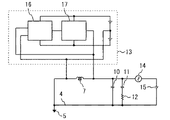
- FIG. 1 is a configuration diagram of a main part of a drive system of an elevator system to which the noise suppression device according to the first embodiment is applied.
- the power supply 1 is provided so as to be able to supply electric power.
- the power source 1 is a commercial power source.
- the motor 2 forms a main part of the hoisting machine of the elevator.
- the control device 3 is provided so as to be able to control the hoisting machine of the elevator.
- the control device 3 is provided so that the electric power from the power source 1 can be supplied to the motor 2 by using an inverter (not shown).
- the ground wire 4 is connected to the power supply 1 and the motor 2 as a reference potential body.
- the ground 5 is connected to the ground wire 4.
- the noise suppression device 6 is provided between the power supply 1 and the control device 3.
- the noise suppression device 6 includes a plurality of common mode coils 7 wound around the same core (not shown), a plurality of input side phase-to-phase capacitors 8, a plurality of output-side phase-to-phase capacitors 9, a first output-side ground-to-ground capacitor 10, and a second output. It includes a side-to-ground capacitor 11, an output side resistor 12, and an electronic device 13.
- the plurality of common mode coils 7 are connected between the power supply 1 and the control device 3.
- the plurality of input-side interphase capacitors 8 are connected between the power supply 1 and the common mode coil 7.
- the plurality of output-side interphase capacitors 9 are connected between the common mode coil 7 and the control device 3.
- the first output-side ground-to-ground capacitor 10 is connected between the plurality of output-side phase-to-ground sensors and the ground wire 4.
- the electronic device 13 is connected in parallel with the common mode coil 7. Specifically, the electronic device 13 is connected to both ends of the winding of the common mode coil 7.
- FIG. 2 is an equivalent circuit of the common mode of the main part of the drive system of the elevator system to which the noise suppression device according to the first embodiment is applied.
- the common mode voltage source 14 corresponds to the common mode voltage generated by the control device 3.
- the ground-to-ground capacity 15 corresponds to the ground-to-ground capacity between the winding of the motor 2 and the housing.
- the common mode voltage is shared by the parallel circuit of the common mode coil 7, the first output side ground-to-ground capacitor 10 and the second output side ground-to-ground capacitor 11, and the ground-to-ground capacitance 15.
- the leakage current flowing through the power supply 1 is determined by the voltage shared by the common mode coil 7 and the impedance characteristics of the common mode coil 7.
- the electronic device 13 includes an arithmetic unit 16 and a power amplifier 17.
- the arithmetic unit 16 detects the voltage applied across the common mode coil 7.
- the arithmetic unit 16 calculates the value of the current to be bypassed from the voltage.
- the power amplifier 17 amplifies the calculation result of the arithmetic unit 16.
- the power amplifier 17 passes the amplified current.
- the electronic device 13 operates so that a low-frequency current among the currents flowing between the power supply 1 and the control device 3 flows in the electronic device, so that the low frequency generated inside the core of the common mode coil 7 is generated. Suppresses the magnetic flux of.
- the series connection between the second output-side ground-to-ground capacitor 11 and the output-side resistor 12 performs resonance damping with the common mode coil 7 that cannot be suppressed by the first output-side ground-to-ground capacitor 10 alone.
- FIG. 3 is a block diagram of a main part of the electronic device of the noise suppression device according to the first embodiment.
- the arithmetic unit 16 includes an error detector 18, a first amplitude amplifier / attenuator 19, a first integrator 20, and an error amplifier 21.
- the error amplifier 21 includes a second amplitude amplifier / attenuator 22, a second integrator 24, a third amplitude amplifier / attenuator 23, and an adder 25.
- the error detector 18 accepts the input of information of the command value and the value of the voltage generated in the common mode coil 7.
- the error detector 18 calculates the difference between the command value and the value of the voltage generated in the common mode coil 7. For example, the error detector 18 calculates the difference between the command value and the voltage value generated in the common mode coil 7 with the command value set to 0.
- the error detector 18 outputs information on the value of the difference.
- the first amplitude amplifier / attenuator 19 accepts the input of the output value information of the error detector 18.
- the first amplitude amplifying / attenuator 19 calculates the amplified value of the output value of the error detector 18.
- the first amplitude amplification / attenuator 19 outputs a value obtained by amplifying the output value from the error detector 18.
- the first integrator 20 accepts the input of the output value information of the first amplitude amplifier / attenuator 19.
- the first integrator 20 calculates a variable value corresponding to a current by integrating the output value of the first amplitude amplifier / attenuator 19.
- the first amplitude amplifier / attenuator 19 outputs information on a variable value corresponding to a current.
- the error amplifier 21 accepts the input of the output value information of the first integrator 20.
- the error amplifier 21 calculates the value obtained by amplifying the output value of the first integrator 20 by using the second amplitude amplifier / attenuator 22, the second integrator 24, the third amplitude amplifier / attenuator 23, and the adder 25. do.
- the error amplifier 21 outputs information on the amplified value of the output value of the first integrator 20.
- the power amplifier 17 accepts input of information on the output value of the error amplifier 21.
- the power amplifier 17 applies a current corresponding to the output value of the error amplifier 21 to a common mode coil 7, a first output side ground-to-ground capacitor 10, a second output-side ground-to-ground capacitor 11, an output-side resistor 12, a ground-to-ground capacitance 15, and the like. Flow to parts.
- the common mode coil 7 the voltage appearing at both ends is determined by the impedance 26 of these components.
- FIG. 4 is a diagram showing a current waveform for explaining the effect of the noise suppression device according to the first embodiment.
- the horizontal axis is time.
- the vertical axis is the current.
- the scale of all axes is the same.
- FIG. 4A shows the waveform of the leakage current to the power supply 1 in the first embodiment.
- FIG. 4B shows the waveform of the leakage current to the power supply 1 when the electronic device 13 is not provided.
- FIG. 4 (c) shows the waveform of the current bypassed by the electronic device 13 in the first embodiment.
- FIG. 4D shows the waveform of the common mode current of the common mode coil 7 in the first embodiment.
- FIG. 4 (e) shows the waveform of the common mode current of the common mode coil 7 when the electronic device 13 is not provided.
- the magnetism When the electronic device 13 is not provided, the magnetism is saturated by the magnetic flux generated in the common mode coil 7. During the period when the magnetism is saturated, the inductance of the common mode coil 7 becomes small. Therefore, as shown in FIGS. 4 (b) and 4 (e), the noise current flows through the power supply 1 and the common mode coil 7 without being suppressed.
- the electronic device 13 bypasses the low frequency current among the currents flowing between the power supply 1 and the device. In this case, magnetic saturation is suppressed in the common mode coil 7. As a result, as shown in FIG. 4A, the high frequency noise current flowing through the power supply 1 is suppressed. As shown in FIG. 4D, only a high frequency noise current flows through the common mode coil 7.
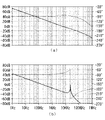
- FIG. 5 is a diagram showing an open loop characteristic for explaining the effect of providing the first output side ground-to-ground capacitor, the second output side ground-to-ground capacitor, and the output side resistor in the noise suppression device according to the first embodiment. be.
- FIG. 5A shows an open loop characteristic when the first output side ground-to-ground capacitor 10, the second output side ground-to-ground capacitor 11, and the output side resistor 12 are provided.
- FIG. 5B shows an open-loop characteristic when the second output-side ground-to-ground capacitor 11 and the output-side resistor 12 are not provided.
- the PI element in which the breaking point frequency is matched with the resonance frequency of the common mode coil 7, the first output side ground-to-ground capacitor 10 and the second output side ground-to-ground capacitor 11 is used as the control system. Has been added.
- the low frequency current of the common mode current flowing between the power supply 1 and the control device 3 flows through the electronic device 13. Specifically, in the electronic device 13, a low-frequency voltage generated in the common-mode coil is detected, and a low-frequency current corresponding to the low-frequency voltage flows, so that the low-frequency current is generated inside the common-mode coil 7. Low frequency magnetic flux is suppressed. Therefore, without the electronic device 13, the low-frequency common-mode current flows, so that the impedance decrease due to magnetic saturation generated in the common-mode coil can be suppressed, and the high-frequency common-mode current can be suppressed more reliably.
- the common mode coil 7 a normal current also flows, but since the voltage component due to the normal mode current is small between the terminals of the common mode coil 7, its influence can be ignored. Therefore, the voltage detection winding of the voltage generated in the common mode coil 7 is shared with the common mode coil 7 that supplies power from the power supply 1 to the control device 3 without newly providing a winding for detecting the voltage in the core of the common mode coil 7. The voltage generated in the common mode coil 7 can be easily detected.
- the noise suppression device 6 includes a first output-side ground-to-ground capacitor 10, a second output-side ground-to-ground capacitor 11, and an output-side resistor 12. Therefore, resonance can be suppressed.
- the electronic device 13 performs a control calculation having the breaking point frequency of the PI element at the resonance frequency of the common mode coil 7, the first output side ground-to-ground capacitor 10, and the second output-side ground-to-ground capacitor 11. Therefore, the degree of freedom in setting the open loop gain can be increased.
- a PI element having a break point frequency may be added to a frequency lower than the break point frequency to improve the open loop gain in the low frequency range.
- the magnetism when the magnetism is saturated in the common mode coil 7 only under a specific condition where the load current is large, a state in which a low frequency current among the currents flowing between the power supply 1 and the control device 3 flows in the electronic device 13. It may be possible to switch whether or not to do so. For example, the input of the arithmetic unit 16 is invalidated, the output of the electronic device 13 is opened, the amplification factor of the error amplifier 21 is lowered, and the current is not bypassed by the electronic device 13 during an unnecessary period. It is also good. In this case, the average calorific value of the power amplifier 17 can be reduced. As a result, a small and inexpensive electronic device 13 can be realized.
- a low-frequency current among the currents flowing between the power supply 1 and the control device 3 flows according to the load applied to the car. You may decide whether or not to make it a state. For example, when the control device 3 supplies electric power for driving an elevator car, a low frequency current among the currents flowing between the power supply 1 and the control device 3 flows according to the speed of the car. You may decide whether or not to do so. In these cases, a small and inexpensive electronic device 13 can be realized in the elevator system.
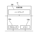
- FIG. 6 is a hardware configuration diagram of the arithmetic unit of the noise suppression device according to the first embodiment.
- Each function of the arithmetic unit 16 can be realized by a processing circuit.
- the processing circuit comprises at least one processor 100a and at least one memory 100b.
- the processing circuit comprises at least one dedicated hardware 200.
- each function of the arithmetic unit 16 is realized by software, firmware, or a combination of software and firmware. At least one of the software and firmware is written as a program. At least one of the software and firmware is stored in at least one memory 100b. At least one processor 100a realizes each function of the arithmetic unit 16 by reading and executing a program stored in at least one memory 100b. At least one processor 100a is also referred to as a central processing unit, a processing unit, an arithmetic unit 16, a microprocessor, a microcomputer, and a DSP.
- At least one memory 100b is a non-volatile or volatile semiconductor memory such as RAM, ROM, flash memory, EPROM, EEPROM, a magnetic disk, a flexible disk, an optical disk, a compact disk, a mini disk, a DVD, or the like.
- the processing circuit comprises at least one dedicated hardware 200
- the processing circuit may be implemented, for example, as a single circuit, a composite circuit, a programmed processor, a parallel programmed processor, an ASIC, an FPGA, or a combination thereof.
- each function of the arithmetic unit 16 is realized by a processing circuit.
- each function of the arithmetic unit 16 is collectively realized by a processing circuit.
- a part may be realized by the dedicated hardware 200, and the other part may be realized by software or firmware.
- the function of the error amplifier 21 is realized by a processing circuit as dedicated hardware 200, and for functions other than the function of the error amplifier 21, at least one processor 100a reads a program stored in at least one memory 100b. It may be realized by executing the above.
- the processing circuit realizes each function of the arithmetic unit 16 by hardware 200, software, firmware, or a combination thereof. It should be noted that this configuration is a configuration when it is realized by a digital circuit, and each function of the arithmetic unit 16 in FIG. 3 may be realized by an analog circuit such as an operational amplifier.
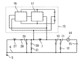
- FIG. 7 is an internal configuration diagram of the electronic device of the noise suppression device according to the first embodiment.
- the same or corresponding parts as those of the first embodiment are designated by the same reference numerals. The explanation of this part is omitted.
- the first input side ground-to-ground capacitor 29 is connected between the wiring between the power supply 1 and the common mode coil 7 and the ground wire 4.
- the second input side ground-to-ground capacitor 30 is connected to the wiring between the power supply 1 and the common mode coil 7.
- the input side resistor 31 is connected between the second input side ground-to-ground capacitor 30 and the ground wire 4.
- the noise suppression device 6 includes a first input-side ground-to-ground capacitor 29, a second input-side ground-to-ground capacitor 30, and an input-side resistor 31. Therefore, even if the wiring on the power supply side 1 is long, the impedance rise on the power supply side can be suppressed, and the stability of the operation of the electronic device 13 can be maintained. Further, the combination of the first output-side ground-to-ground capacitor 10, the second output-side ground-to-ground capacitor 11, and the output-side resistor 12 lowers the impedance between the high-frequency terminals of the common mode coil 7. Therefore, it is possible to suppress an increase in the voltage between the terminals of the common mode coil 7 due to high frequency noise. As a result, the power supply voltage required for the power amplifier 17 can be suppressed, and the heat generation of the power amplifier 17 can be suppressed.
- the noise suppression device of the present disclosure can be used for an elevator system.
Landscapes
- Engineering & Computer Science (AREA)
- Power Engineering (AREA)
- Physics & Mathematics (AREA)
- Electromagnetism (AREA)
- Inverter Devices (AREA)
- Power Conversion In General (AREA)
- Filters And Equalizers (AREA)
- Dc-Dc Converters (AREA)
Abstract
Description
図1は実施の形態1におけるノイズ抑制装置が適用されるエレベーターシステムの駆動系の要部の構成図である。
図2は実施の形態1におけるノイズ抑制装置が適用されるエレベーターシステムの駆動系の要部のコモンモードの等価回路である。
図3は実施の形態1におけるノイズ抑制装置の電子装置の要部の構成図である。
図4は実施の形態1におけるノイズ抑制装置の効果を説明するための電流波形を示す図である。図4において、横軸は時間である。縦軸は電流である。全ての軸の縮尺は同じである。
図5は実施の形態1におけるノイズ抑制装置において第1出力側対地間コンデンサと第2出力側対地間コンデンサと出力側抵抗とが設けられることによる効果を説明するためのオープンループ特性を示す図である。
図6は実施の形態1におけるノイズ抑制装置の演算装置のハードウェア構成図である。
図7は実施の形態1におけるノイズ抑制装置の電子装置の内部構成図である。なお、実施の形態1の部分と同一又は相当部分には同一符号が付される。当該部分の説明は省略される。
Claims (11)
- 電源と制御装置との間に接続されたコモンモードコイルと、
前記コモンモードコイルと並列に接続され、前記電源と前記制御装置との間に流れる電流のうちの低周波の電流が流れる電子装置と、
を備えたノイズ抑制装置。 - 前記電子装置は、前記コモンモードコイルに発生する低周波の電圧を検出し、当該低周波の電圧に対応した低周波の電流が流れることで、前記コモンモードコイルの内部に発生する低周波の磁束を抑制する請求項1に記載のノイズ抑制装置。
- 前記コモンモードコイルに発生する低周波電圧の検出手段は、ノーマル電流が流れるコモンモードコイルである請求項1または請求項2に記載のノイズ抑制装置。
- 前記コモンモードコイルと前記制御装置との間の配線に接続された出力側対地間コンデンサと、
前記出力側対地間コンデンサと基準電位体との間に接続された出力側抵抗と、
を備えた請求項1から請求項3のいずれか一項に記載のノイズ抑制装置。 - 前記コモンモードコイルと前記制御装置との間の配線と基準電位体との間に接続された出力側コンデンサ、
を備えた請求項1から請求項4のいずれか一項に記載のノイズ抑制装置。 - 前記電源と前記コモンモードコイルとの間の配線に接続された入力側対地間コンデンサと、
前記入力側対地間コンデンサと基準電位体との間に接続された入力側抵抗と、
を備えた請求項1から請求項5のいずれか一項に記載のノイズ抑制装置。 - 前記電源と前記コモンモードコイルとの間の配線と基準電位体との間に接続された入力側コンデンサ、
を備えた請求項1から請求項6のいずれか一項に記載のノイズ抑制装置。 - 前記電子装置は、前記電源と前記制御装置との間の素子における共振周波数にPI要素の折れ点周波数を持つ制御演算を行う請求項1から請求項7のいずれか一項に記載のノイズ抑制装置。
- 前記電子装置は、前記電源と前記制御装置との間に流れる電流のうちの低周波の電流が流れる状態とするか否かが切替自在に設けられた請求項1から請求項8のいずれか一項に記載のノイズ抑制装置。
- 前記電子装置は、前記制御装置がエレベーターのかごの駆動させるための電力を供給する際に、前記かごにかかる負荷に応じて、前記電源と前記制御装置との間に流れる電流のうちの低周波の電流が流れる状態とするか否かを決める請求項9に記載のノイズ抑制装置。
- 前記電子装置は、前記制御装置がエレベーターのかごの駆動させるための電力を供給する際に、前記かごの速度に応じて、前記電源と前記制御装置との間に流れる電流のうちの低周波の電流が流れる状態とするか否かを決める請求項9または請求項10に記載のノイズ抑制装置。
Priority Applications (6)
| Application Number | Priority Date | Filing Date | Title |
|---|---|---|---|
| KR1020237021649A KR20230110351A (ko) | 2021-01-05 | 2021-01-05 | 노이즈 억제 장치 |
| DE112021006755.9T DE112021006755T5 (de) | 2021-01-05 | 2021-01-05 | Rauschunterdrückungsvorrichtung |
| JP2022573821A JP7513120B2 (ja) | 2021-01-05 | 2021-01-05 | ノイズ抑制装置 |
| CN202180088207.7A CN116648844A (zh) | 2021-01-05 | 2021-01-05 | 噪声抑制装置 |
| US18/265,969 US12614970B2 (en) | 2021-01-05 | 2021-01-05 | Noise suppression device |
| PCT/JP2021/000125 WO2022149192A1 (ja) | 2021-01-05 | 2021-01-05 | ノイズ抑制装置 |
Applications Claiming Priority (1)
| Application Number | Priority Date | Filing Date | Title |
|---|---|---|---|
| PCT/JP2021/000125 WO2022149192A1 (ja) | 2021-01-05 | 2021-01-05 | ノイズ抑制装置 |
Publications (1)
| Publication Number | Publication Date |
|---|---|
| WO2022149192A1 true WO2022149192A1 (ja) | 2022-07-14 |
Family
ID=82358141
Family Applications (1)
| Application Number | Title | Priority Date | Filing Date |
|---|---|---|---|
| PCT/JP2021/000125 Ceased WO2022149192A1 (ja) | 2021-01-05 | 2021-01-05 | ノイズ抑制装置 |
Country Status (6)
| Country | Link |
|---|---|
| US (1) | US12614970B2 (ja) |
| JP (1) | JP7513120B2 (ja) |
| KR (1) | KR20230110351A (ja) |
| CN (1) | CN116648844A (ja) |
| DE (1) | DE112021006755T5 (ja) |
| WO (1) | WO2022149192A1 (ja) |
Citations (5)
| Publication number | Priority date | Publication date | Assignee | Title |
|---|---|---|---|---|
| JPH05292668A (ja) * | 1992-04-13 | 1993-11-05 | Mels Corp | ノイズフィルター |
| JPH11122909A (ja) * | 1997-10-16 | 1999-04-30 | Fuji Electric Co Ltd | 電力変換装置のノイズフィルタ |
| JP2013145940A (ja) * | 2012-01-13 | 2013-07-25 | Nec Network Products Ltd | 雑音抑制回路および雑音抑制方法 |
| JP2017011895A (ja) * | 2015-06-23 | 2017-01-12 | 田淵電機株式会社 | 高周波零相電流遮断用インバータ回路 |
| JP2017118387A (ja) * | 2015-12-25 | 2017-06-29 | 富士電機株式会社 | ノイズフィルタ |
Family Cites Families (10)
| Publication number | Priority date | Publication date | Assignee | Title |
|---|---|---|---|---|
| JP3044650B2 (ja) | 1996-03-27 | 2000-05-22 | 勲 高橋 | 電力変換装置のノイズ低減装置 |
| US6271651B1 (en) * | 2000-04-20 | 2001-08-07 | Volterra Semiconductor Corporation | Inductor shorting switch for a switching voltage regulator |
| FR2902247B1 (fr) | 2006-06-07 | 2008-08-15 | Schneider Toshiba Inverter | Dispositif de filtrage cem dans un variateur de vitesse |
| US8786371B2 (en) * | 2011-11-18 | 2014-07-22 | Skyworks Solutions, Inc. | Apparatus and methods for voltage converters |
| JP5705144B2 (ja) | 2012-01-27 | 2015-04-22 | 三菱電機株式会社 | 高周波電流低減装置および検出トランス |
| US10177702B2 (en) * | 2015-08-12 | 2019-01-08 | Samsung Electronics Co., Ltd. | Conduction noise filtering circuit, inverting device, and compressor |
| US10498238B2 (en) * | 2017-10-30 | 2019-12-03 | Renesas Electronics America Inc. | Synthetic ripple generator for low power hysteretic buck-boost DC-DC controller |
| US10454370B2 (en) * | 2018-03-14 | 2019-10-22 | Alpha And Omega Semiconductor (Cayman) Limited | Three quarter bridge for buck-derived switch-mode power supplies |
| WO2020251045A1 (ja) * | 2019-06-14 | 2020-12-17 | ローム株式会社 | スイッチング電源装置 |
| JP7619258B2 (ja) * | 2021-12-28 | 2025-01-22 | 株式会社豊田自動織機 | 電力供給装置 |
-
2021
- 2021-01-05 JP JP2022573821A patent/JP7513120B2/ja active Active
- 2021-01-05 DE DE112021006755.9T patent/DE112021006755T5/de active Pending
- 2021-01-05 WO PCT/JP2021/000125 patent/WO2022149192A1/ja not_active Ceased
- 2021-01-05 CN CN202180088207.7A patent/CN116648844A/zh active Pending
- 2021-01-05 KR KR1020237021649A patent/KR20230110351A/ko not_active Ceased
- 2021-01-05 US US18/265,969 patent/US12614970B2/en active Active
Patent Citations (5)
| Publication number | Priority date | Publication date | Assignee | Title |
|---|---|---|---|---|
| JPH05292668A (ja) * | 1992-04-13 | 1993-11-05 | Mels Corp | ノイズフィルター |
| JPH11122909A (ja) * | 1997-10-16 | 1999-04-30 | Fuji Electric Co Ltd | 電力変換装置のノイズフィルタ |
| JP2013145940A (ja) * | 2012-01-13 | 2013-07-25 | Nec Network Products Ltd | 雑音抑制回路および雑音抑制方法 |
| JP2017011895A (ja) * | 2015-06-23 | 2017-01-12 | 田淵電機株式会社 | 高周波零相電流遮断用インバータ回路 |
| JP2017118387A (ja) * | 2015-12-25 | 2017-06-29 | 富士電機株式会社 | ノイズフィルタ |
Also Published As
| Publication number | Publication date |
|---|---|
| CN116648844A (zh) | 2023-08-25 |
| KR20230110351A (ko) | 2023-07-21 |
| JPWO2022149192A1 (ja) | 2022-07-14 |
| DE112021006755T5 (de) | 2023-10-19 |
| US20240097557A1 (en) | 2024-03-21 |
| JP7513120B2 (ja) | 2024-07-09 |
| US12614970B2 (en) | 2026-04-28 |
Similar Documents
| Publication | Publication Date | Title |
|---|---|---|
| US8823448B1 (en) | Feed forward active EMI filters | |
| CN107462773B (zh) | 负载检测器 | |
| US10436828B2 (en) | Load detector | |
| US20080080106A1 (en) | Integrated DC link inductor and common mode current sensor winding | |
| JP6785878B2 (ja) | 電力変換装置 | |
| US20170164127A1 (en) | Audio processing system | |
| JP6568743B2 (ja) | 伝導性ノイズ抑制回路及びインバータ装置 | |
| JP2017521675A5 (ja) | ||
| JP6153387B2 (ja) | 電流センサ | |
| CN101114540A (zh) | 线圈组及使用该线圈组的电子装置 | |
| US20140023198A1 (en) | Method and circuit for testing an audio high-frequency loudspeaker being part of a loudspeaker system | |
| US20090027136A1 (en) | Active electromagnetic interference filter circuit for suppressing a line conducted interference signal | |
| WO2023073984A1 (ja) | コモンモードフィルタ | |
| US11258411B2 (en) | Amplifier with an at least second order filter in the control loop | |
| WO2016067576A1 (ja) | 異常検出装置 | |
| JP7513120B2 (ja) | ノイズ抑制装置 | |
| JP2008271628A (ja) | 電流検出回路 | |
| JPH10294633A (ja) | Acラインフィルタ | |
| JP7597127B2 (ja) | スイッチング電源装置 | |
| WO2025057926A1 (ja) | 電流センサ及び測定装置 | |
| JP2007526729A (ja) | 誘導電流検出装置を有さない能動emiフィルタ | |
| JP3511999B2 (ja) | モータ制御装置及びそれを有する機器 | |
| JPS6236340Y2 (ja) | ||
| JPH05244790A (ja) | リニアモータ制御回路 | |
| JPWO2013011903A1 (ja) | 増幅回路及び増幅方法 |
Legal Events
| Date | Code | Title | Description |
|---|---|---|---|
| 121 | Ep: the epo has been informed by wipo that ep was designated in this application |
Ref document number: 21917420 Country of ref document: EP Kind code of ref document: A1 |
|
| ENP | Entry into the national phase |
Ref document number: 2022573821 Country of ref document: JP Kind code of ref document: A |
|
| WWE | Wipo information: entry into national phase |
Ref document number: 18265969 Country of ref document: US |
|
| ENP | Entry into the national phase |
Ref document number: 20237021649 Country of ref document: KR Kind code of ref document: A |
|
| WWE | Wipo information: entry into national phase |
Ref document number: 202180088207.7 Country of ref document: CN |
|
| WWE | Wipo information: entry into national phase |
Ref document number: 112021006755 Country of ref document: DE |
|
| 122 | Ep: pct application non-entry in european phase |
Ref document number: 21917420 Country of ref document: EP Kind code of ref document: A1 |
|
| WWR | Wipo information: refused in national office |
Ref document number: 1020237021649 Country of ref document: KR |