WO2022145223A1 - カバー部材、金型装置および電子装置 - Google Patents
カバー部材、金型装置および電子装置 Download PDFInfo
- Publication number
- WO2022145223A1 WO2022145223A1 PCT/JP2021/046173 JP2021046173W WO2022145223A1 WO 2022145223 A1 WO2022145223 A1 WO 2022145223A1 JP 2021046173 W JP2021046173 W JP 2021046173W WO 2022145223 A1 WO2022145223 A1 WO 2022145223A1
- Authority
- WO
- WIPO (PCT)
- Prior art keywords
- cover member
- mold
- thick portion
- ceiling wall
- eject pin
- Prior art date
- Legal status (The legal status is an assumption and is not a legal conclusion. Google has not performed a legal analysis and makes no representation as to the accuracy of the status listed.)
- Ceased
Links
Images




Classifications
-
- B—PERFORMING OPERATIONS; TRANSPORTING
- B29—WORKING OF PLASTICS; WORKING OF SUBSTANCES IN A PLASTIC STATE IN GENERAL
- B29C—SHAPING OR JOINING OF PLASTICS; SHAPING OF MATERIAL IN A PLASTIC STATE, NOT OTHERWISE PROVIDED FOR; AFTER-TREATMENT OF THE SHAPED PRODUCTS, e.g. REPAIRING
- B29C39/00—Shaping by casting, i.e. introducing the moulding material into a mould or between confining surfaces without significant moulding pressure; Apparatus therefor
- B29C39/22—Component parts, details or accessories; Auxiliary operations
- B29C39/26—Moulds or cores
-
- H—ELECTRICITY
- H05—ELECTRIC TECHNIQUES NOT OTHERWISE PROVIDED FOR
- H05K—PRINTED CIRCUITS; CASINGS OR CONSTRUCTIONAL DETAILS OF ELECTRIC APPARATUS; MANUFACTURE OF ASSEMBLAGES OF ELECTRICAL COMPONENTS
- H05K5/00—Casings, cabinets or drawers for electric apparatus
- H05K5/0026—Casings, cabinets or drawers for electric apparatus provided with connectors and printed circuit boards [PCB], e.g. automotive electronic control units
- H05K5/0047—Casings, cabinets or drawers for electric apparatus provided with connectors and printed circuit boards [PCB], e.g. automotive electronic control units having a two-part housing enclosing a PCB
-
- B—PERFORMING OPERATIONS; TRANSPORTING
- B29—WORKING OF PLASTICS; WORKING OF SUBSTANCES IN A PLASTIC STATE IN GENERAL
- B29C—SHAPING OR JOINING OF PLASTICS; SHAPING OF MATERIAL IN A PLASTIC STATE, NOT OTHERWISE PROVIDED FOR; AFTER-TREATMENT OF THE SHAPED PRODUCTS, e.g. REPAIRING
- B29C45/00—Injection moulding, i.e. forcing the required volume of moulding material through a nozzle into a closed mould; Apparatus therefor
- B29C45/17—Component parts, details or accessories; Auxiliary operations
- B29C45/40—Removing or ejecting moulded articles
- B29C45/4005—Ejector constructions; Ejector operating mechanisms
- B29C45/401—Ejector pin constructions or mountings
-
- H—ELECTRICITY
- H05—ELECTRIC TECHNIQUES NOT OTHERWISE PROVIDED FOR
- H05K—PRINTED CIRCUITS; CASINGS OR CONSTRUCTIONAL DETAILS OF ELECTRIC APPARATUS; MANUFACTURE OF ASSEMBLAGES OF ELECTRICAL COMPONENTS
- H05K5/00—Casings, cabinets or drawers for electric apparatus
- H05K5/0026—Casings, cabinets or drawers for electric apparatus provided with connectors and printed circuit boards [PCB], e.g. automotive electronic control units
- H05K5/0047—Casings, cabinets or drawers for electric apparatus provided with connectors and printed circuit boards [PCB], e.g. automotive electronic control units having a two-part housing enclosing a PCB
- H05K5/0052—Casings, cabinets or drawers for electric apparatus provided with connectors and printed circuit boards [PCB], e.g. automotive electronic control units having a two-part housing enclosing a PCB characterized by joining features of the housing parts
-
- H—ELECTRICITY
- H05—ELECTRIC TECHNIQUES NOT OTHERWISE PROVIDED FOR
- H05K—PRINTED CIRCUITS; CASINGS OR CONSTRUCTIONAL DETAILS OF ELECTRIC APPARATUS; MANUFACTURE OF ASSEMBLAGES OF ELECTRICAL COMPONENTS
- H05K5/00—Casings, cabinets or drawers for electric apparatus
- H05K5/02—Details
- H05K5/03—Covers
-
- B—PERFORMING OPERATIONS; TRANSPORTING
- B29—WORKING OF PLASTICS; WORKING OF SUBSTANCES IN A PLASTIC STATE IN GENERAL
- B29C—SHAPING OR JOINING OF PLASTICS; SHAPING OF MATERIAL IN A PLASTIC STATE, NOT OTHERWISE PROVIDED FOR; AFTER-TREATMENT OF THE SHAPED PRODUCTS, e.g. REPAIRING
- B29C45/00—Injection moulding, i.e. forcing the required volume of moulding material through a nozzle into a closed mould; Apparatus therefor
- B29C45/0025—Preventing defects on the moulded article, e.g. weld lines, shrinkage marks
-
- B—PERFORMING OPERATIONS; TRANSPORTING
- B29—WORKING OF PLASTICS; WORKING OF SUBSTANCES IN A PLASTIC STATE IN GENERAL
- B29L—INDEXING SCHEME ASSOCIATED WITH SUBCLASS B29C, RELATING TO PARTICULAR ARTICLES
- B29L2031/00—Other particular articles
- B29L2031/34—Electrical apparatus, e.g. sparking plugs or parts thereof
- B29L2031/3481—Housings or casings incorporating or embedding electric or electronic elements
Definitions
- the present invention relates to a cover member molded from a synthetic resin material, a mold device for molding the cover member, and an electronic device using the cover member.
- a circuit board on which electronic components are mounted is housed in an internal space of a housing consisting of a metal case body and a synthetic resin cover.
- the cover in such a housing is provided with a ceiling wall, which is usually opposed to the circuit board, and a side wall around the ceiling wall, in order to secure a space for accommodating the circuit board from the case body. It has a dish-like shape and is molded using a mold by a technique such as injection molding.
- the mold device In resin molding using a mold, the mold device is generally equipped with an eject pin that extrudes the molded product in order to release the molded product from the mold surface of the mold after opening the mold. Is. That is, the eject pin operates in parallel with the opening / closing direction of the mold, and the eject pin protrudes from the mold surface, so that the molded product is pushed by the eject pin and released from the mold.
- Patent Document 1 discloses a configuration in which the tip surface of an eject pin exposed on the mold surface of a mold is rounded into a spherical shape.
- Patent Document 1 cannot solve the problem of dents that occur when the eject pin is extruded.
- the cover member is relatively thicker than the adjacent ceiling wall general portion at a plurality of locations on the ceiling wall corresponding to the ejection position by the eject pin at the time of mold release. A thick portion that protrudes inward locally is provided so as to become meat.
- the tip surface of the eject pin is pressed against the thick part at the time of mold release, so even if a stamp-like dent is generated by the eject pin, it is possible to secure a wall thickness equal to or greater than that of the general part of the surrounding ceiling wall. It is possible to avoid a decrease in strength. Therefore, the wall thickness of the ceiling wall itself other than the thick part can be sufficiently thinned.
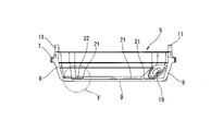
- FIG. 2 is a cross-sectional view taken along the line AA of FIG.
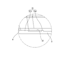
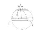
- An enlarged cross-sectional view of a thick portion obtained by enlarging the E portion of FIG. Enlarged plan view of the thick part.
- An enlarged plan view of a thick portion showing an example in which the dent is displaced due to the contact of the eject pin.
- Sectional drawing of the breathing filter part The front view of the breathing filter part seen along the arrow B direction of FIG.
- Explanatory drawing which showed the positional relationship between the gate position at the time of mold molding, the final arrival point of a resin material, and a thick part.
- Sectional view of the assembled electronic device The plan view which looked at the cover of 2nd Example from the inside.
- FIG. 12 is a cross-sectional view taken along the line CC of FIG.
- FIG. 3 is an enlarged cross-sectional view of a thick portion in which the F portion of FIG. 13 is enlarged.
- Explanatory drawing which showed the dimensional relationship between an eject pin and a thick part.
- the perspective view of the mold apparatus which molds the cover of 1st Embodiment.
- Explanatory drawing in the state where the mold is opened.
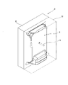
- FIG. 1 is an exploded perspective view of the electronic device 1 of the first embodiment.
- the electronic device 1 is attached to an appropriate position of the vehicle as, for example, a controller of an automatic transmission for a vehicle, and includes a housing 2 and a circuit board 3 housed in the internal space of the housing 2. ing.
- the housing 2 is composed of a substantially rectangular base 4 made of a metal such as aluminum, and a synthetic resin cover 5 having a shape bulging so as to cover the circuit board 3 in the housing 2.
- the base 4 and the cover 5 correspond to the "case” and the “cover member” in the claims, respectively.
- the base 4 has a relatively thin rectangular plate shape, and is made of a die-cast product made of a metal material such as aluminum, for example.
- the base 4 has a flange portion 4a along one plane on the peripheral edge, and the central portion 4b surrounded by the flange portion 4a has a shape slightly recessed to the side opposite to the cover 5.
- the central portion 4b generally corresponds to the region where the circuit boards 3 are overlapped.
- a slightly raised heat sink portion 4c is appropriately formed in the central portion 4b.
- the heat sink portion 4c adheres to a heat-generating component (not shown) attached to the circuit board 3 via, for example, heat-dissipating grease, and functions as a heat sink.
- the base 4 includes a total of four mounting pieces 4d for mounting the entire electronic device 1 on the vehicle body. Further, circular mounting holes 4e for assembling with the cover 5 are opened at the four corners of the base 4.
- the cover 5 is integrally molded of a thermoplastic synthetic resin material such as a polyamide resin, and has a rectangular box shape or a deep dish shape with an open surface toward the base 4.
- the flange portions 7 corresponding to the flange portions 4a of the base 4 are provided on three sides of the peripheral edge, and the ceiling wall 9 and the flange portions are substantially flat via the side wall 8 that rises diagonally from these flange portions 7. 7 is connected.
- a bulging portion 10 opened so as to receive the connector 15 described later is provided on the remaining one side.
- the ceiling wall 9 is along a plane substantially parallel to the plane along which the flange portion 7 is.
- heat caulking pins 11 projecting in a direction orthogonal to the surface of the flange portion 7 are provided. These heat caulking pins 11 are located at positions corresponding to the mounting holes 4e of the base 4, and are crushed as so-called heat caulking by inserting them into the mounting holes 4e and then heating and pressurizing them from the outside of the base 4. It will be in the state of being. In the assembled state of the electronic device 1, the base 4 and the cover 5 are firmly assembled by heat caulking at these four locations. In FIG. 1, the heat caulking pin 11 before the heat caulking process is shown.
- the base 4 and the cover 5 are sealed by a gasket 12 provided along the flange portions 4a and 7, respectively.
- a gasket 13 is also provided around the connector 15, and the gasket 13 seals between the bulging portion 10 of the cover 5 and the connector 15.
- the circuit board 3 is a printed wiring board using a resin substrate such as glass epoxy resin or a metal substrate, and has a rectangular shape corresponding to the shape of the housing 2.
- a synthetic resin connector 15 for connecting a power supply line and a signal line together is attached to one end of the circuit board 3 in the longitudinal direction. In the assembled state of the electronic device 1, a part of the connector 15 is exposed to the outside through between the bulging portion 10 of the cover 5 and the base 4 described above.
- the circuit board 3 is fixed to the base 4 by screws 16 arranged at its four corners.
- a large number of electronic components including a CPU, an IC, a resistor, a capacitor, and the like are mounted on the circuit board 3. It should be noted that the figure shows only a part of a large number of electronic components.
- a plurality of (for example, four) electrolytic capacitors 17 are included as electronic components having the maximum height from the circuit board 3.
- the electrolytic capacitor 17 has a prismatic shape in the illustrated example, and a predetermined gap is required between the top surface thereof and the inner surface surface of the cover 5 so that gas can be discharged for explosion proof.
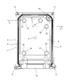
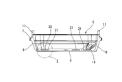
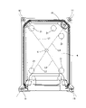
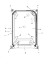
- FIG. 2 is a plan view of the cover 5 of the first embodiment as viewed from the inside (circuit board 3 side), and FIG. 3 is a cross-sectional view taken along the line AA of FIG.
- the entire cover 5 is integrally molded by mold molding, for example, injection molding.
- the substantially rectangular ceiling wall 9 surrounded by the side wall 8 on three sides and the bulging portion 10 on the remaining one side has a flat plate shape parallel to the base 4 and the circuit board 3. And basically has a certain wall thickness.
- thick portions 21 forming a circular shape in a plan view are provided at a plurality of locations (five locations in the illustrated example) near the side wall 8 around the ceiling wall 9.
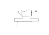
- the thick portion 21 is formed so as to locally project inward so as to be relatively thicker than the general portion of the ceiling wall 9 adjacent to the thick portion 21. There is no unevenness on the outer surface of the ceiling wall 9 due to the formation of the thick portion 21, and therefore the outer surface of the ceiling wall 9 is a flat surface.
- the thick portion 21 that protrudes in a disk shape toward the inside of the cover 5 in this way is arranged corresponding to the extrusion position by the eject pin provided in the mold device at the time of injection molding.
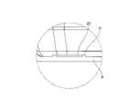
- FIG. 4 is an enlarged cross-sectional view of the thick portion 21, and
- FIG. 5 is an enlarged plan view of the thick portion 21.
- the eject pin has a round bar shape
- the thick portion 21 has a size including an extruded surface by the eject pin (that is, the tip surface of the eject pin in contact with the molded product).
- the tip of the eject pin is pressed against each other to form a circular recess 22 in the center of the thick portion 21.
- the depth of the recess 22 will be slightly different due to manufacturing variations (for example, variations in the temperature of the molded product when extruded by the eject pin) and the like.
- the cross-sectional view of FIG. 4 shows the case where the dent 22 is generated at the maximum depth, and when the dent 22 is the maximum expected depth as shown in the figure, the dent 22 portion.
- the wall thickness of the ceiling wall 9 is set to be equal to the wall thickness of the surrounding general part. In other words, the wall thickness of the ceiling wall 9 at the recess 22 portion is secured to be equal to or higher than the wall thickness of the general portion even if there are manufacturing variations.
- FIG. 6 is an enlarged cross-sectional view of the thick portion 21 before contact with the eject pin, and is formed into a disk-shaped shape as shown in FIG. 6 in the mold.
- the final product that has been extruded by the eject pin has an annular shape having a recess 22 as shown in FIGS. 4 and 5.
- the ceiling wall 9 is locally excessively thin even if the dent 22 is generated by being pushed by the eject pin. There is no concern that the strength will decrease due to the dent 22. Therefore, the ceiling wall 9 can be sufficiently thinned.
- FIG. 11 is a cross-sectional view of the electronic device 1 provided with the cover 5 of the first embodiment, in particular, the electrolytic capacitor 17 which is an electronic component having the maximum height from the circuit board 3 and the ceiling wall of the cover 5.
- the height relationship with the inner surface of 9 is shown.
- the distance from the circuit board 3 in the thick portion 21 to the surface of the thick portion 21 is set slightly larger than the height dimension of the electrolytic capacitor 17.
- the electrolytic capacitor 17 and the thick portion 21 are arranged so as not to overlap each other. That is, the top surface of the electrolytic capacitor 17 faces the general portion of the ceiling wall 9 other than the thick portion 21, and a sufficient gap is secured between the two.
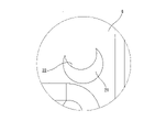
- the thick portion 21 of the first embodiment also contributes to the determination of whether or not the eject pin correctly extrudes the molded product. That is, as shown in FIGS. 4 and 5, since the round bar-shaped eject pin and the circular thick portion 21 are arranged concentrically, when the dent 22 is generated, the thick portion 21 remains in an annular shape. It becomes a shape. On the other hand, when the ejected position of the eject pin is displaced due to distortion of the molded product at the time of mold release, the recess 22 is formed not concentrically but biased with respect to the outer circle of the thick portion 21 as shown in FIG. In an extreme case, the thick portion 21 remains in a crescent shape as shown in the figure.
- FIG. 10 is an explanatory diagram showing the positional relationship between the gate position G at the time of mold molding, the final arrival point of the resin material, and the thick portion 21.
- the gate serving as the injection port of the molten resin during injection molding is located substantially at the center of the ceiling wall 9 as shown by reference numeral G in FIG.
- the molten resin material flows radially from this gate position G.
- the final destination of the resin material is the heat caulking pins 11 located at the four corners of the cover 5.
- the above-mentioned thick portion 21 is basically located between the gate position G and the heat caulking pin 11 which is the final destination. Specifically, it is arranged on the straight lines L1 to L4 connecting the gate position G and the heat caulking pin 11. However, since a circular opening 19 serving as a breathing filter portion is provided on the straight line L4, the configuration is different.
- the other three thick portions 21 are located on the straight lines L1, L2, and L3, respectively.
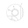
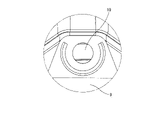
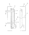
- FIG. 8 is a cross-sectional view of the breathing filter section
- FIG. 9 is a front view of the breathing filter section as viewed along the arrow B direction of FIG.
- the opening 19 serving as the breathing filter portion is located at one corner portion of the cover 5, and as shown in FIGS. 8 and 9, the side wall 8 is formed to be thick and the opening 19 has a circular cross section. Is formed through.
- a water-repellent filter film (not shown) is attached to the inner end surface of the cover 5 of the opening 19.
- the straight line L4 is paired on both sides of the straight line L4.
- the thick portion 21 is arranged. These two thick portions 21 are arranged at positions that are as symmetrical as possible with the straight line L4 interposed therebetween. Therefore, the resin material flows around the opening 19 from both sides via the pair of thick portions 21 to the heat caulking pin 11 which is the final destination. As a result, the flow of the resin becomes good also in the vicinity of the breathing filter portion.
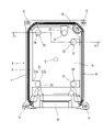
- FIG. 12 is a plan view of the cover 5 of the second embodiment as viewed from the inside
- FIG. 13 is a sectional view taken along the line CC of FIG. 12
- FIG. 14 is an enlarged sectional view of the thick portion 21.
- 15 is an enlarged cross-sectional view of a thick portion before contact with the eject pin.
- the thick portion 21 of the cover 5 of the second embodiment has a shape in which the thick portion 21 of the first embodiment described above is connected to an adjacent side wall 8.
- the thick portion 21 of the second embodiment is composed of a semicircular portion 21a and a rectangular portion 21b sandwiched between two parallel straight lines extending tangentially from the semicircular portion 21a, and is a rectangular portion.
- the tip of 21b is connected to the side wall 8. That is, the thick portion 21 and the side wall 8 are formed into a continuous shape.
- the five thick portions 21 function as a kind of reinforcing member for strengthening the ceiling wall 9, the heat shrinkage of the ceiling wall 9 of the molded product is suppressed, and the ceiling wall 9 is less likely to warp.
- the area occupied by the thick portion 21 in the plan view of the cover 5 is larger than that in the first embodiment, but as in the first embodiment, electrolysis is performed at a position overlapping the thick portion 21 in the plan view.
- the capacitor 17 is not arranged. Since the number of electronic components arranged on the outer peripheral edge of the circuit board 3 is relatively small, the adverse effect on the layout of the electronic components due to the increase in the area occupied by the thick portion 21 is small.
- the eject pin is pressed against the thick portion 21 in the same manner as in the first embodiment, and as a result of the eject pin being pressed against the thick portion 21 molded as shown in FIG. 15, the final molded product has a final molded product.
- a circular recess 22 corresponding to the tip surface of the eject pin is formed.
- the diameter of the semicircular portion 21a is larger than the diameter of the round bar-shaped eject pin. That is, the thick portion 21 has a size including the extruded surface by the eject pin.
- FIG. 16 is a plan view of the cover 5 of the third embodiment as viewed from the inside
- FIG. 17 is an explanatory view showing the dimensional relationship between the tip portion of the eject pin 25 and the thick portion 21.
- a total of five circular thick portions 21 are arranged at the same positions as in the first embodiment.
- the diameter of the molded circular thick portion 21 is relatively smaller than the diameter of the eject pin 25. That is, the thick portion 21 has a size included in the extruded surface by the eject pin 25.
- the electrolytic capacitor 17 can be arranged at a position where it overlaps with the thick portion 21 in a plan view, and the layout of electronic components can be arranged. The degree of freedom increases.
- the eject pin has been described as having a round bar shape, but in the present invention, the eject pin may have any shape such as a quadrangular cross section, a polygonal shape, or an elliptical shape.
- the contour shape of the portion 21 is not limited to a circle, and may be a quadrangle, a polygon, an ellipse, or the like.
- FIG. 18 is a perspective view of the mold device 31 for molding the cover 5 of the first embodiment.
- the mold device 31 includes a first mold 32 which is a so-called core mold and a second mold 33 which is a so-called cavity mold, and both of them form a space, that is, a cavity 34 corresponding to the shape of the molded product. Will be done.
- the mold device 31 also includes a slide core or the like for forming the above-mentioned opening 19, but is omitted in the drawing.
- the gate G into which the molten resin is injected from the injection device is located at the center of the ceiling wall 9.
- the molten resin flowing in from the gate G at the center of the ceiling wall 9 flows radially in the relatively narrow cavity 34 constituting the ceiling wall 9, and reaches the heat caulking pins 11 at the four corners, which are the final destinations of the resin material. Head to.
- FIG. 19 shows a mold device 31 in a state where molding is completed and the mold is opened.
- the inner surface of the cover 5 is molded by the first mold 32, and the cover 5 is formed by the second mold 33.
- the outer surface is molded.
- a plurality of eject pins 25 are provided so as to penetrate the first mold 32. When the molded product is cooled to some extent, the molds 32 and 33 are opened, and the eject pin 25 pushes out the molded product in conjunction with the mold opening.
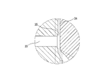
- FIG. 20 is an enlarged view of part D in FIG. As shown in FIG. 20, a disk-shaped recess 35 forming the thick portion 21 is provided on the mold surface of the first mold 32 that forms the inner surface of the cover 5. The recess 35 is provided at a position facing the eject pin 25, and becomes a part of the cavity 34 into which the resin material flows.
- the present invention is not limited to the above embodiment and various modifications can be made.
- the cover member of the present invention is not limited to the cover of the controller described above, and can be widely applied to various cover members having a ceiling wall and a side wall.
- the cover member of the present invention has a ceiling wall and a side wall, and is a cover member formed of a synthetic resin material using a molding die. Thick parts that locally protrude inward at multiple locations on the ceiling wall so that they are relatively thicker than the general part of the adjacent ceiling wall, corresponding to the position of being pushed out by the eject pin at the time of mold release. Is provided.
- the thick portion has a size including the extruded surface by the eject pin.
- the thick portion has a size included in the extruded surface by the eject pin.
- the thick portion is arranged on a straight line connecting the gate position at the time of mold molding and the final arrival point of the resin material.
- the side wall has an opening, and a pair of thick portions are arranged on both sides of a straight line connecting the center of the opening and the gate position at the time of molding.
- the opening is located on a straight line connecting the gate position and the final destination of the resin material.
- the thick portion is formed so as to be connected to the side wall.
- the mold device of the present invention is a mold device for molding the cover member according to any one of claims 1 to 7. It has at least a first mold for molding the inner surface of the cover member and a second mold for molding the outer surface of the cover member.
- the first mold is provided with a plurality of eject pins for extruding and releasing the molded cover member.
- a recess for forming the thick portion is formed corresponding to the position of the eject pin.
- the electronic device of the present invention is housed in a space formed by the cover member according to any one of claims 1 to 7, a case combined with the cover member, and the cover member and the case. It is an electronic device equipped with a circuit board on which electronic components are mounted. The distance from the circuit board to the surface of the thick portion in the thick portion is set larger than the height dimension of the electronic component having the maximum height from the circuit board among the electronic components. There is.
Landscapes
- Engineering & Computer Science (AREA)
- Microelectronics & Electronic Packaging (AREA)
- Manufacturing & Machinery (AREA)
- Mechanical Engineering (AREA)
- Moulds For Moulding Plastics Or The Like (AREA)
Abstract
Description
離型時のイジェクトピンによる押し出し位置にそれぞれ対応して、上記天井壁の複数箇所に、隣接する天井壁一般部よりも相対的に厚肉となるように局部的に内側に突出した厚肉部が設けられている。
上記カバー部材の内側面を成形する第1の金型と上記カバー部材の外側面を成形する第2の金型とを少なくとも有し、
上記第1の金型は、成形されたカバー部材を押し出して離型させる複数のイジェクトピンを備えており、
上記第1の金型の型面には、上記イジェクトピンの位置に対応して、上記厚肉部を形成するための凹部が形成されている。
上記電子部品の中で上記回路基板からの高さが最大である電子部品の高さ寸法に比較して、上記厚肉部における上記回路基板から該厚肉部表面までの距離が大きく設定されている。
Claims (9)
- 天井壁と側壁とを有し、成形型を用いて合成樹脂材料により成形されてなるカバー部材であって、
離型時のイジェクトピンによる押し出し位置にそれぞれ対応して、上記天井壁の複数箇所に、隣接する天井壁一般部よりも相対的に厚肉となるように局部的に内側に突出した厚肉部が設けられている、カバー部材。 - 上記厚肉部は、上記イジェクトピンによる押し出し面を包含する大きさを有している、請求項1に記載のカバー部材。
- 上記厚肉部は、上記イジェクトピンによる押し出し面に包含される大きさを有している、請求項1に記載のカバー部材。
- 型成形時のゲート位置と樹脂材料の最終到達点とを結ぶ直線上に上記厚肉部が配置されている、請求項1~3のいずれかに記載のカバー部材。
- 上記側壁に開口部を有し、この開口部の中心と型成形時のゲート位置とを結ぶ直線の両側に一対の厚肉部が配置されている、請求項1~3のいずれかに記載のカバー部材。
- 上記開口部は、上記ゲート位置と樹脂材料の最終到達点とを結ぶ直線上に位置している、請求項5に記載のカバー部材。
- 上記厚肉部は、上記側壁に接続された形に形成されている、請求項1または2に記載のカバー部材。
- 請求項1~7のいずれかに記載のカバー部材を成形するための金型装置であって、
上記カバー部材の内側面を成形する第1の金型と上記カバー部材の外側面を成形する第2の金型とを少なくとも有し、
上記第1の金型は、成形されたカバー部材を押し出して離型させる複数のイジェクトピンを備えており、
上記第1の金型の型面には、上記イジェクトピンの位置に対応して、上記厚肉部を形成するための凹部が形成されている、
金型装置。 - 請求項1~7のいずれかに記載のカバー部材と、このカバー部材に組み合わされるケースと、上記カバー部材と上記ケースとで形成される空間内に収容され、かつ電子部品が実装された回路基板と、を備えた電子装置であって、
上記電子部品の中で上記回路基板からの高さが最大である電子部品の高さ寸法に比較して、上記厚肉部における上記回路基板から該厚肉部表面までの距離が大きく設定されている、電子装置。
Priority Applications (4)
| Application Number | Priority Date | Filing Date | Title |
|---|---|---|---|
| CN202180088137.5A CN116648343A (zh) | 2020-12-28 | 2021-12-15 | 外壳部件、金属模型装置及电子装置 |
| JP2022572982A JPWO2022145223A1 (ja) | 2020-12-28 | 2021-12-15 | |
| US18/259,560 US20240051192A1 (en) | 2020-12-28 | 2021-12-15 | Cover member, mold device, and electronic device |
| DE112021006691.9T DE112021006691T5 (de) | 2020-12-28 | 2021-12-15 | Abdeckelement, Formvorrichtung und elektronische Vorrichtung |
Applications Claiming Priority (2)
| Application Number | Priority Date | Filing Date | Title |
|---|---|---|---|
| JP2020-218158 | 2020-12-28 | ||
| JP2020218158 | 2020-12-28 |
Publications (1)
| Publication Number | Publication Date |
|---|---|
| WO2022145223A1 true WO2022145223A1 (ja) | 2022-07-07 |
Family
ID=82260678
Family Applications (1)
| Application Number | Title | Priority Date | Filing Date |
|---|---|---|---|
| PCT/JP2021/046173 Ceased WO2022145223A1 (ja) | 2020-12-28 | 2021-12-15 | カバー部材、金型装置および電子装置 |
Country Status (5)
| Country | Link |
|---|---|
| US (1) | US20240051192A1 (ja) |
| JP (1) | JPWO2022145223A1 (ja) |
| CN (1) | CN116648343A (ja) |
| DE (1) | DE112021006691T5 (ja) |
| WO (1) | WO2022145223A1 (ja) |
Citations (4)
| Publication number | Priority date | Publication date | Assignee | Title |
|---|---|---|---|---|
| JPH06210683A (ja) * | 1993-01-18 | 1994-08-02 | Sekisui Chem Co Ltd | 射出成形用金型 |
| JPH0852769A (ja) * | 1994-08-11 | 1996-02-27 | Fujitsu Ltd | 樹脂成形用金型 |
| JP2001113353A (ja) * | 1999-10-15 | 2001-04-24 | Fujitsu Kasei Kk | マグネシウム合金用射出成形用型装置 |
| JP2005178066A (ja) * | 2003-12-17 | 2005-07-07 | Munekata Co Ltd | 射出成形方法及びこの成形方法により成形された成形品 |
Family Cites Families (9)
| Publication number | Priority date | Publication date | Assignee | Title |
|---|---|---|---|---|
| JP2000334760A (ja) | 1999-05-28 | 2000-12-05 | Kumamoto Nippon Denki Kk | 樹脂成形用の金型装置及びこれを備えた樹脂成形装置 |
| KR100725789B1 (ko) * | 2005-06-30 | 2007-06-08 | 삼성전자주식회사 | 금형장치 |
| US7722792B2 (en) * | 2007-02-05 | 2010-05-25 | Canon Kabushiki Kaisha | Injection mold and partial compression molding method |
| JP5110130B2 (ja) * | 2010-07-27 | 2012-12-26 | 株式会社デンソー | 車載電子制御ユニット用筺体 |
| JP5965706B2 (ja) * | 2012-04-12 | 2016-08-10 | 日立オートモティブシステムズ株式会社 | 流量センサの製造方法 |
| DE102013207668A1 (de) * | 2013-04-26 | 2014-10-30 | Bayerische Motoren Werke Aktiengesellschaft | Werkzeug zur Herstellung eines Faser-Kunststoff-Verbund-Bauteils mit wenigstens einer Entlüftungsbohrung und darin angeordnetem Auswerferstift |
| JP6094548B2 (ja) * | 2014-08-29 | 2017-03-15 | 株式会社デンソー | 電子装置収容筐体 |
| CN107836139A (zh) * | 2015-09-04 | 2018-03-23 | 日立汽车系统株式会社 | 车载控制装置 |
| DE102015016784B4 (de) * | 2015-12-23 | 2018-12-20 | Fm Marketing Gmbh | Monolitische Fernbedienung und Verfahren zur Herstellung derselben |
-
2021
- 2021-12-15 CN CN202180088137.5A patent/CN116648343A/zh active Pending
- 2021-12-15 JP JP2022572982A patent/JPWO2022145223A1/ja active Pending
- 2021-12-15 WO PCT/JP2021/046173 patent/WO2022145223A1/ja not_active Ceased
- 2021-12-15 US US18/259,560 patent/US20240051192A1/en active Pending
- 2021-12-15 DE DE112021006691.9T patent/DE112021006691T5/de active Pending
Patent Citations (4)
| Publication number | Priority date | Publication date | Assignee | Title |
|---|---|---|---|---|
| JPH06210683A (ja) * | 1993-01-18 | 1994-08-02 | Sekisui Chem Co Ltd | 射出成形用金型 |
| JPH0852769A (ja) * | 1994-08-11 | 1996-02-27 | Fujitsu Ltd | 樹脂成形用金型 |
| JP2001113353A (ja) * | 1999-10-15 | 2001-04-24 | Fujitsu Kasei Kk | マグネシウム合金用射出成形用型装置 |
| JP2005178066A (ja) * | 2003-12-17 | 2005-07-07 | Munekata Co Ltd | 射出成形方法及びこの成形方法により成形された成形品 |
Also Published As
| Publication number | Publication date |
|---|---|
| CN116648343A (zh) | 2023-08-25 |
| DE112021006691T5 (de) | 2023-10-12 |
| JPWO2022145223A1 (ja) | 2022-07-07 |
| US20240051192A1 (en) | 2024-02-15 |
Similar Documents
| Publication | Publication Date | Title |
|---|---|---|
| US8357015B2 (en) | Metal-resin compound member | |
| JP2013232312A (ja) | カード部材及びカードエッジコネクタ並びにカード部材の製造方法 | |
| US10070542B2 (en) | Electronic-circuit unit and manufacturing method thereof | |
| TW202329798A (zh) | 功率模組及功率裝置 | |
| TWI700574B (zh) | 殼體、電子裝置及殼體的製作方法 | |
| EP2442381A1 (en) | Battery pack case and method for manufacturing same, and battery pack and method for manufacturing same | |
| KR102509124B1 (ko) | 감광 어셈블리, 이미징 모듈, 인텔리전트 단말 및 감광 어셈블리의 제조 방법과 몰드 | |
| CN110603693B (zh) | 电子模块和制造方法 | |
| US20240051192A1 (en) | Cover member, mold device, and electronic device | |
| JP6973970B2 (ja) | コアユニット及びリアクトル | |
| US20180374773A1 (en) | Heat sink and electronic component device | |
| CN114434729A (zh) | 半导体装置用的框体的制造方法 | |
| JP2014093451A (ja) | モールドパッケージの製造方法 | |
| JP3177101U (ja) | 成形金型 | |
| CN105874666B (zh) | 电子电路单元的外壳的成型方法 | |
| JP4800759B2 (ja) | 電子タグの製造方法およびその製造方法に適した保護ケース | |
| CN114885546A (zh) | 电子产品外壳、注塑成型方法及制作方法 | |
| CN113496956A (zh) | 半导体装置及半导体装置的制造方法 | |
| JP6610460B2 (ja) | 電子装置、及び、電子装置の製造方法 | |
| JP2004193372A (ja) | 表面実装部品用ケース、表面実装電子部品および表面実装電子部品の製造方法 | |
| JPH11145637A (ja) | サーボアンプの筐体 | |
| JP4086534B2 (ja) | メモリーカードとその成形方法 | |
| JP3117683B2 (ja) | 非接触型半導体カード | |
| WO2025074982A1 (ja) | 光学センサーパッケージ | |
| JPH06226776A (ja) | 電磁波シールド機能をもつ筺体の製造方法 |
Legal Events
| Date | Code | Title | Description |
|---|---|---|---|
| 121 | Ep: the epo has been informed by wipo that ep was designated in this application |
Ref document number: 21915084 Country of ref document: EP Kind code of ref document: A1 |
|
| ENP | Entry into the national phase |
Ref document number: 2022572982 Country of ref document: JP Kind code of ref document: A |
|
| WWE | Wipo information: entry into national phase |
Ref document number: 18259560 Country of ref document: US |
|
| WWE | Wipo information: entry into national phase |
Ref document number: 202180088137.5 Country of ref document: CN |
|
| WWE | Wipo information: entry into national phase |
Ref document number: 112021006691 Country of ref document: DE |
|
| 122 | Ep: pct application non-entry in european phase |
Ref document number: 21915084 Country of ref document: EP Kind code of ref document: A1 |