WO2022138747A1 - 回路接続用接着剤フィルム、並びに、回路接続構造体及びその製造方法 - Google Patents
回路接続用接着剤フィルム、並びに、回路接続構造体及びその製造方法 Download PDFInfo
- Publication number
- WO2022138747A1 WO2022138747A1 PCT/JP2021/047653 JP2021047653W WO2022138747A1 WO 2022138747 A1 WO2022138747 A1 WO 2022138747A1 JP 2021047653 W JP2021047653 W JP 2021047653W WO 2022138747 A1 WO2022138747 A1 WO 2022138747A1
- Authority
- WO
- WIPO (PCT)
- Prior art keywords
- adhesive layer
- circuit connection
- electrode
- component
- adhesive
- Prior art date
Links
- 239000002313 adhesive film Substances 0.000 title claims abstract description 190
- 238000004519 manufacturing process Methods 0.000 title claims abstract description 68
- 238000000034 method Methods 0.000 title claims abstract description 67
- 239000012790 adhesive layer Substances 0.000 claims abstract description 372
- 239000002245 particle Substances 0.000 claims abstract description 187
- 150000001875 compounds Chemical class 0.000 claims description 79
- -1 acrylate compound Chemical class 0.000 claims description 70
- 239000010410 layer Substances 0.000 claims description 68
- 239000000853 adhesive Substances 0.000 claims description 64
- 230000001070 adhesive effect Effects 0.000 claims description 64
- 238000002788 crimping Methods 0.000 claims description 64
- 229920005989 resin Polymers 0.000 claims description 50
- 239000011347 resin Substances 0.000 claims description 50
- 229920001187 thermosetting polymer Polymers 0.000 claims description 48
- 238000011156 evaluation Methods 0.000 claims description 38
- 239000011521 glass Substances 0.000 claims description 36
- 239000000463 material Substances 0.000 claims description 30
- 239000004593 Epoxy Substances 0.000 claims description 24
- 239000003795 chemical substances by application Substances 0.000 claims description 23
- 239000011256 inorganic filler Substances 0.000 claims description 21
- 229910003475 inorganic filler Inorganic materials 0.000 claims description 21
- 150000001451 organic peroxides Chemical class 0.000 claims description 10
- RWSOTUBLDIXVET-UHFFFAOYSA-N Dihydrogen sulfide Chemical class S RWSOTUBLDIXVET-UHFFFAOYSA-N 0.000 claims description 8
- 150000003863 ammonium salts Chemical class 0.000 claims description 7
- 238000005259 measurement Methods 0.000 claims description 6
- NIXOWILDQLNWCW-UHFFFAOYSA-M Acrylate Chemical compound [O-]C(=O)C=C NIXOWILDQLNWCW-UHFFFAOYSA-M 0.000 description 92
- 239000000203 mixture Substances 0.000 description 77
- IISBACLAFKSPIT-UHFFFAOYSA-N bisphenol A Chemical compound C=1C=C(O)C=CC=1C(C)(C)C1=CC=C(O)C=C1 IISBACLAFKSPIT-UHFFFAOYSA-N 0.000 description 25
- 150000001252 acrylic acid derivatives Chemical class 0.000 description 23
- 239000000758 substrate Substances 0.000 description 19
- 238000010438 heat treatment Methods 0.000 description 17
- 239000002966 varnish Substances 0.000 description 17
- LYCAIKOWRPUZTN-UHFFFAOYSA-N Ethylene glycol Chemical compound OCCO LYCAIKOWRPUZTN-UHFFFAOYSA-N 0.000 description 15
- 239000010419 fine particle Substances 0.000 description 15
- VYPSYNLAJGMNEJ-UHFFFAOYSA-N Silicium dioxide Chemical compound O=[Si]=O VYPSYNLAJGMNEJ-UHFFFAOYSA-N 0.000 description 13
- 150000001768 cations Chemical class 0.000 description 13
- 230000000694 effects Effects 0.000 description 13
- 150000003254 radicals Chemical class 0.000 description 13
- ZWEHNKRNPOVVGH-UHFFFAOYSA-N 2-Butanone Chemical compound CCC(C)=O ZWEHNKRNPOVVGH-UHFFFAOYSA-N 0.000 description 11
- 150000001450 anions Chemical class 0.000 description 11
- 229920002799 BoPET Polymers 0.000 description 10
- 238000010030 laminating Methods 0.000 description 10
- 239000000126 substance Substances 0.000 description 10
- 125000003700 epoxy group Chemical group 0.000 description 9
- 239000003960 organic solvent Substances 0.000 description 9
- 239000003822 epoxy resin Substances 0.000 description 8
- 229910052751 metal Inorganic materials 0.000 description 8
- 239000002184 metal Substances 0.000 description 8
- 229920003023 plastic Polymers 0.000 description 8
- 239000004033 plastic Substances 0.000 description 8
- 229920000647 polyepoxide Polymers 0.000 description 8
- 239000002253 acid Substances 0.000 description 7
- 125000003118 aryl group Chemical group 0.000 description 7
- 239000006059 cover glass Substances 0.000 description 7
- WXZMFSXDPGVJKK-UHFFFAOYSA-N pentaerythritol Chemical compound OCC(CO)(CO)CO WXZMFSXDPGVJKK-UHFFFAOYSA-N 0.000 description 7
- 239000003505 polymerization initiator Substances 0.000 description 7
- 239000000377 silicon dioxide Substances 0.000 description 7
- 239000000654 additive Substances 0.000 description 6
- WGCNASOHLSPBMP-UHFFFAOYSA-N hydroxyacetaldehyde Natural products OCC=O WGCNASOHLSPBMP-UHFFFAOYSA-N 0.000 description 6
- 238000009413 insulation Methods 0.000 description 6
- 238000002156 mixing Methods 0.000 description 6
- 150000003839 salts Chemical class 0.000 description 6
- OKTJSMMVPCPJKN-UHFFFAOYSA-N Carbon Chemical compound [C] OKTJSMMVPCPJKN-UHFFFAOYSA-N 0.000 description 5
- 125000003647 acryloyl group Chemical group O=C([*])C([H])=C([H])[H] 0.000 description 5
- 238000004220 aggregation Methods 0.000 description 5
- 230000002776 aggregation Effects 0.000 description 5
- 125000002723 alicyclic group Chemical group 0.000 description 5
- PXKLMJQFEQBVLD-UHFFFAOYSA-N bisphenol F Chemical class C1=CC(O)=CC=C1CC1=CC=C(O)C=C1 PXKLMJQFEQBVLD-UHFFFAOYSA-N 0.000 description 5
- 229910052799 carbon Inorganic materials 0.000 description 5
- 239000011248 coating agent Substances 0.000 description 5
- 238000000576 coating method Methods 0.000 description 5
- 230000000052 comparative effect Effects 0.000 description 5
- 239000000470 constituent Substances 0.000 description 5
- 239000000945 filler Substances 0.000 description 5
- 230000009477 glass transition Effects 0.000 description 5
- 150000002923 oximes Chemical class 0.000 description 5
- ZOXJGFHDIHLPTG-UHFFFAOYSA-N Boron Chemical compound [B] ZOXJGFHDIHLPTG-UHFFFAOYSA-N 0.000 description 4
- 239000004642 Polyimide Substances 0.000 description 4
- 239000004793 Polystyrene Substances 0.000 description 4
- 125000000217 alkyl group Chemical group 0.000 description 4
- 125000002029 aromatic hydrocarbon group Chemical group 0.000 description 4
- 238000005452 bending Methods 0.000 description 4
- 229910052796 boron Inorganic materials 0.000 description 4
- 125000004432 carbon atom Chemical group C* 0.000 description 4
- NIHNNTQXNPWCJQ-UHFFFAOYSA-N fluorene Chemical compound C1=CC=C2CC3=CC=CC=C3C2=C1 NIHNNTQXNPWCJQ-UHFFFAOYSA-N 0.000 description 4
- 125000000524 functional group Chemical group 0.000 description 4
- QSHDDOUJBYECFT-UHFFFAOYSA-N mercury Chemical compound [Hg] QSHDDOUJBYECFT-UHFFFAOYSA-N 0.000 description 4
- 229910052753 mercury Inorganic materials 0.000 description 4
- 125000000962 organic group Chemical group 0.000 description 4
- 125000001997 phenyl group Chemical group [H]C1=C([H])C([H])=C(*)C([H])=C1[H] 0.000 description 4
- 229920001721 polyimide Polymers 0.000 description 4
- 229920002223 polystyrene Polymers 0.000 description 4
- 238000002360 preparation method Methods 0.000 description 4
- 239000002904 solvent Substances 0.000 description 4
- 238000003860 storage Methods 0.000 description 4
- 125000001424 substituent group Chemical group 0.000 description 4
- LWNGJAHMBMVCJR-UHFFFAOYSA-N (2,3,4,5,6-pentafluorophenoxy)boronic acid Chemical compound OB(O)OC1=C(F)C(F)=C(F)C(F)=C1F LWNGJAHMBMVCJR-UHFFFAOYSA-N 0.000 description 3
- CDDDRVNOHLVEED-UHFFFAOYSA-N 1-cyclohexyl-3-[1-[[1-(cyclohexylcarbamoylamino)cyclohexyl]diazenyl]cyclohexyl]urea Chemical compound C1CCCCC1(N=NC1(CCCCC1)NC(=O)NC1CCCCC1)NC(=O)NC1CCCCC1 CDDDRVNOHLVEED-UHFFFAOYSA-N 0.000 description 3
- CSCPPACGZOOCGX-UHFFFAOYSA-N Acetone Chemical compound CC(C)=O CSCPPACGZOOCGX-UHFFFAOYSA-N 0.000 description 3
- XEKOWRVHYACXOJ-UHFFFAOYSA-N Ethyl acetate Chemical compound CCOC(C)=O XEKOWRVHYACXOJ-UHFFFAOYSA-N 0.000 description 3
- DNIAPMSPPWPWGF-UHFFFAOYSA-N Propylene glycol Chemical compound CC(O)CO DNIAPMSPPWPWGF-UHFFFAOYSA-N 0.000 description 3
- RTAQQCXQSZGOHL-UHFFFAOYSA-N Titanium Chemical class [Ti] RTAQQCXQSZGOHL-UHFFFAOYSA-N 0.000 description 3
- YXFVVABEGXRONW-UHFFFAOYSA-N Toluene Chemical compound CC1=CC=CC=C1 YXFVVABEGXRONW-UHFFFAOYSA-N 0.000 description 3
- 239000000919 ceramic Substances 0.000 description 3
- 150000004292 cyclic ethers Chemical group 0.000 description 3
- 239000012954 diazonium Substances 0.000 description 3
- MTHSVFCYNBDYFN-UHFFFAOYSA-N diethylene glycol Chemical compound OCCOCCO MTHSVFCYNBDYFN-UHFFFAOYSA-N 0.000 description 3
- VFHVQBAGLAREND-UHFFFAOYSA-N diphenylphosphoryl-(2,4,6-trimethylphenyl)methanone Chemical compound CC1=CC(C)=CC(C)=C1C(=O)P(=O)(C=1C=CC=CC=1)C1=CC=CC=C1 VFHVQBAGLAREND-UHFFFAOYSA-N 0.000 description 3
- 238000001035 drying Methods 0.000 description 3
- 230000007717 exclusion Effects 0.000 description 3
- 125000001153 fluoro group Chemical group F* 0.000 description 3
- RAXXELZNTBOGNW-UHFFFAOYSA-N imidazole Natural products C1=CNC=N1 RAXXELZNTBOGNW-UHFFFAOYSA-N 0.000 description 3
- 239000004615 ingredient Substances 0.000 description 3
- 239000003999 initiator Substances 0.000 description 3
- 239000002923 metal particle Substances 0.000 description 3
- PXHVJJICTQNCMI-UHFFFAOYSA-N nickel Substances [Ni] PXHVJJICTQNCMI-UHFFFAOYSA-N 0.000 description 3
- UMRZSTCPUPJPOJ-KNVOCYPGSA-N norbornane Chemical group C1C[C@H]2CC[C@@H]1C2 UMRZSTCPUPJPOJ-KNVOCYPGSA-N 0.000 description 3
- 229920003986 novolac Polymers 0.000 description 3
- NFHFRUOZVGFOOS-UHFFFAOYSA-N palladium;triphenylphosphane Chemical compound [Pd].C1=CC=CC=C1P(C=1C=CC=CC=1)C1=CC=CC=C1.C1=CC=CC=C1P(C=1C=CC=CC=1)C1=CC=CC=C1.C1=CC=CC=C1P(C=1C=CC=CC=1)C1=CC=CC=C1.C1=CC=CC=C1P(C=1C=CC=CC=1)C1=CC=CC=C1 NFHFRUOZVGFOOS-UHFFFAOYSA-N 0.000 description 3
- 229920006287 phenoxy resin Polymers 0.000 description 3
- 239000013034 phenoxy resin Substances 0.000 description 3
- PAYRUJLWNCNPSJ-UHFFFAOYSA-O phenylazanium Chemical class [NH3+]C1=CC=CC=C1 PAYRUJLWNCNPSJ-UHFFFAOYSA-O 0.000 description 3
- 150000004714 phosphonium salts Chemical class 0.000 description 3
- 238000005498 polishing Methods 0.000 description 3
- 239000004417 polycarbonate Substances 0.000 description 3
- 229920000515 polycarbonate Polymers 0.000 description 3
- 229920001223 polyethylene glycol Polymers 0.000 description 3
- 229920000139 polyethylene terephthalate Polymers 0.000 description 3
- 239000005020 polyethylene terephthalate Substances 0.000 description 3
- 238000006116 polymerization reaction Methods 0.000 description 3
- 239000004065 semiconductor Substances 0.000 description 3
- 229920005992 thermoplastic resin Polymers 0.000 description 3
- PUPZLCDOIYMWBV-UHFFFAOYSA-N (+/-)-1,3-Butanediol Chemical compound CC(O)CCO PUPZLCDOIYMWBV-UHFFFAOYSA-N 0.000 description 2
- OZAIFHULBGXAKX-UHFFFAOYSA-N 2-(2-cyanopropan-2-yldiazenyl)-2-methylpropanenitrile Chemical compound N#CC(C)(C)N=NC(C)(C)C#N OZAIFHULBGXAKX-UHFFFAOYSA-N 0.000 description 2
- 125000003903 2-propenyl group Chemical group [H]C([*])([H])C([H])=C([H])[H] 0.000 description 2
- 229910017008 AsF 6 Inorganic materials 0.000 description 2
- 229930185605 Bisphenol Natural products 0.000 description 2
- KAKZBPTYRLMSJV-UHFFFAOYSA-N Butadiene Chemical compound C=CC=C KAKZBPTYRLMSJV-UHFFFAOYSA-N 0.000 description 2
- PEDCQBHIVMGVHV-UHFFFAOYSA-N Glycerine Chemical compound OCC(O)CO PEDCQBHIVMGVHV-UHFFFAOYSA-N 0.000 description 2
- CERQOIWHTDAKMF-UHFFFAOYSA-M Methacrylate Chemical compound CC(=C)C([O-])=O CERQOIWHTDAKMF-UHFFFAOYSA-M 0.000 description 2
- OKKJLVBELUTLKV-UHFFFAOYSA-N Methanol Chemical class OC OKKJLVBELUTLKV-UHFFFAOYSA-N 0.000 description 2
- 241000209094 Oryza Species 0.000 description 2
- 235000007164 Oryza sativa Nutrition 0.000 description 2
- KDLHZDBZIXYQEI-UHFFFAOYSA-N Palladium Chemical compound [Pd] KDLHZDBZIXYQEI-UHFFFAOYSA-N 0.000 description 2
- ISWSIDIOOBJBQZ-UHFFFAOYSA-N Phenol Chemical compound OC1=CC=CC=C1 ISWSIDIOOBJBQZ-UHFFFAOYSA-N 0.000 description 2
- 239000004952 Polyamide Substances 0.000 description 2
- 239000002202 Polyethylene glycol Substances 0.000 description 2
- 229910018286 SbF 6 Inorganic materials 0.000 description 2
- 239000006087 Silane Coupling Agent Substances 0.000 description 2
- XUIMIQQOPSSXEZ-UHFFFAOYSA-N Silicon Chemical compound [Si] XUIMIQQOPSSXEZ-UHFFFAOYSA-N 0.000 description 2
- PPBRXRYQALVLMV-UHFFFAOYSA-N Styrene Chemical compound C=CC1=CC=CC=C1 PPBRXRYQALVLMV-UHFFFAOYSA-N 0.000 description 2
- GWEVSGVZZGPLCZ-UHFFFAOYSA-N Titan oxide Chemical compound O=[Ti]=O GWEVSGVZZGPLCZ-UHFFFAOYSA-N 0.000 description 2
- XLOMVQKBTHCTTD-UHFFFAOYSA-N Zinc monoxide Chemical compound [Zn]=O XLOMVQKBTHCTTD-UHFFFAOYSA-N 0.000 description 2
- MCMNRKCIXSYSNV-UHFFFAOYSA-N Zirconium dioxide Chemical compound O=[Zr]=O MCMNRKCIXSYSNV-UHFFFAOYSA-N 0.000 description 2
- NIXOWILDQLNWCW-UHFFFAOYSA-N acrylic acid group Chemical group C(C=C)(=O)O NIXOWILDQLNWCW-UHFFFAOYSA-N 0.000 description 2
- PNEYBMLMFCGWSK-UHFFFAOYSA-N aluminium oxide Inorganic materials [O-2].[O-2].[O-2].[Al+3].[Al+3] PNEYBMLMFCGWSK-UHFFFAOYSA-N 0.000 description 2
- MWPLVEDNUUSJAV-UHFFFAOYSA-N anthracene Chemical compound C1=CC=CC2=CC3=CC=CC=C3C=C21 MWPLVEDNUUSJAV-UHFFFAOYSA-N 0.000 description 2
- WERYXYBDKMZEQL-UHFFFAOYSA-N butane-1,4-diol Chemical compound OCCCCO WERYXYBDKMZEQL-UHFFFAOYSA-N 0.000 description 2
- 238000011088 calibration curve Methods 0.000 description 2
- 238000006243 chemical reaction Methods 0.000 description 2
- 239000011247 coating layer Substances 0.000 description 2
- 229910052802 copper Inorganic materials 0.000 description 2
- 239000010949 copper Substances 0.000 description 2
- 150000001989 diazonium salts Chemical class 0.000 description 2
- 229910052737 gold Inorganic materials 0.000 description 2
- 239000010931 gold Substances 0.000 description 2
- 230000005484 gravity Effects 0.000 description 2
- 125000004435 hydrogen atom Chemical group [H]* 0.000 description 2
- XMBWDFGMSWQBCA-UHFFFAOYSA-N hydrogen iodide Chemical class I XMBWDFGMSWQBCA-UHFFFAOYSA-N 0.000 description 2
- 230000001771 impaired effect Effects 0.000 description 2
- 230000001678 irradiating effect Effects 0.000 description 2
- 238000004898 kneading Methods 0.000 description 2
- 125000005439 maleimidyl group Chemical group C1(C=CC(N1*)=O)=O 0.000 description 2
- 229910052759 nickel Inorganic materials 0.000 description 2
- 239000012766 organic filler Substances 0.000 description 2
- 125000003566 oxetanyl group Chemical group 0.000 description 2
- BASFCYQUMIYNBI-UHFFFAOYSA-N platinum Chemical compound [Pt] BASFCYQUMIYNBI-UHFFFAOYSA-N 0.000 description 2
- 229920002647 polyamide Polymers 0.000 description 2
- 229920001451 polypropylene glycol Polymers 0.000 description 2
- 229920001296 polysiloxane Polymers 0.000 description 2
- 229920000131 polyvinylidene Polymers 0.000 description 2
- 238000003825 pressing Methods 0.000 description 2
- 239000011164 primary particle Substances 0.000 description 2
- 230000008569 process Effects 0.000 description 2
- 230000009257 reactivity Effects 0.000 description 2
- 239000011342 resin composition Substances 0.000 description 2
- 235000009566 rice Nutrition 0.000 description 2
- 229910052710 silicon Inorganic materials 0.000 description 2
- 239000010703 silicon Substances 0.000 description 2
- 229910052709 silver Inorganic materials 0.000 description 2
- 238000003756 stirring Methods 0.000 description 2
- 230000001629 suppression Effects 0.000 description 2
- 238000012360 testing method Methods 0.000 description 2
- 238000012719 thermal polymerization Methods 0.000 description 2
- 238000012546 transfer Methods 0.000 description 2
- 125000002023 trifluoromethyl group Chemical group FC(F)(F)* 0.000 description 2
- JXCAHDJDIAQCJO-UHFFFAOYSA-N (1-tert-butylperoxy-2-ethylhexyl) hydrogen carbonate Chemical compound CCCCC(CC)C(OC(O)=O)OOC(C)(C)C JXCAHDJDIAQCJO-UHFFFAOYSA-N 0.000 description 1
- MAOBFOXLCJIFLV-UHFFFAOYSA-N (2-aminophenyl)-phenylmethanone Chemical group NC1=CC=CC=C1C(=O)C1=CC=CC=C1 MAOBFOXLCJIFLV-UHFFFAOYSA-N 0.000 description 1
- FVQMJJQUGGVLEP-UHFFFAOYSA-N (2-methylpropan-2-yl)oxy 2-ethylhexaneperoxoate Chemical compound CCCCC(CC)C(=O)OOOC(C)(C)C FVQMJJQUGGVLEP-UHFFFAOYSA-N 0.000 description 1
- HCXVPNKIBYLBIT-UHFFFAOYSA-N (2-methylpropan-2-yl)oxy 3,5,5-trimethylhexaneperoxoate Chemical compound CC(C)(C)CC(C)CC(=O)OOOC(C)(C)C HCXVPNKIBYLBIT-UHFFFAOYSA-N 0.000 description 1
- QEQBMZQFDDDTPN-UHFFFAOYSA-N (2-methylpropan-2-yl)oxy benzenecarboperoxoate Chemical compound CC(C)(C)OOOC(=O)C1=CC=CC=C1 QEQBMZQFDDDTPN-UHFFFAOYSA-N 0.000 description 1
- MCVVDMSWCQUKEV-UHFFFAOYSA-N (2-nitrophenyl)methyl 4-methylbenzenesulfonate Chemical compound C1=CC(C)=CC=C1S(=O)(=O)OCC1=CC=CC=C1[N+]([O-])=O MCVVDMSWCQUKEV-UHFFFAOYSA-N 0.000 description 1
- DLDWUFCUUXXYTB-UHFFFAOYSA-N (2-oxo-1,2-diphenylethyl) 4-methylbenzenesulfonate Chemical compound C1=CC(C)=CC=C1S(=O)(=O)OC(C=1C=CC=CC=1)C(=O)C1=CC=CC=C1 DLDWUFCUUXXYTB-UHFFFAOYSA-N 0.000 description 1
- UNMJLQGKEDTEKJ-UHFFFAOYSA-N (3-ethyloxetan-3-yl)methanol Chemical compound CCC1(CO)COC1 UNMJLQGKEDTEKJ-UHFFFAOYSA-N 0.000 description 1
- NLBJAOHLJABDAU-UHFFFAOYSA-N (3-methylbenzoyl) 3-methylbenzenecarboperoxoate Chemical compound CC1=CC=CC(C(=O)OOC(=O)C=2C=C(C)C=CC=2)=C1 NLBJAOHLJABDAU-UHFFFAOYSA-N 0.000 description 1
- MVELOSYXCOVILT-UHFFFAOYSA-N (4-hydroxy-2-methylpentan-2-yl) 7,7-dimethyloctaneperoxoate Chemical compound CC(O)CC(C)(C)OOC(=O)CCCCCC(C)(C)C MVELOSYXCOVILT-UHFFFAOYSA-N 0.000 description 1
- AGKBXKFWMQLFGZ-UHFFFAOYSA-N (4-methylbenzoyl) 4-methylbenzenecarboperoxoate Chemical compound C1=CC(C)=CC=C1C(=O)OOC(=O)C1=CC=C(C)C=C1 AGKBXKFWMQLFGZ-UHFFFAOYSA-N 0.000 description 1
- NOBYOEQUFMGXBP-UHFFFAOYSA-N (4-tert-butylcyclohexyl) (4-tert-butylcyclohexyl)oxycarbonyloxy carbonate Chemical compound C1CC(C(C)(C)C)CCC1OC(=O)OOC(=O)OC1CCC(C(C)(C)C)CC1 NOBYOEQUFMGXBP-UHFFFAOYSA-N 0.000 description 1
- RIPYNJLMMFGZSX-UHFFFAOYSA-N (5-benzoylperoxy-2,5-dimethylhexan-2-yl) benzenecarboperoxoate Chemical compound C=1C=CC=CC=1C(=O)OOC(C)(C)CCC(C)(C)OOC(=O)C1=CC=CC=C1 RIPYNJLMMFGZSX-UHFFFAOYSA-N 0.000 description 1
- BLKRGXCGFRXRNQ-SNAWJCMRSA-N (z)-3-carbonoperoxoyl-4,4-dimethylpent-2-enoic acid Chemical compound OC(=O)/C=C(C(C)(C)C)\C(=O)OO BLKRGXCGFRXRNQ-SNAWJCMRSA-N 0.000 description 1
- BEQKKZICTDFVMG-UHFFFAOYSA-N 1,2,3,4,6-pentaoxepane-5,7-dione Chemical compound O=C1OOOOC(=O)O1 BEQKKZICTDFVMG-UHFFFAOYSA-N 0.000 description 1
- ALVZNPYWJMLXKV-UHFFFAOYSA-N 1,9-Nonanediol Chemical compound OCCCCCCCCCO ALVZNPYWJMLXKV-UHFFFAOYSA-N 0.000 description 1
- 125000001637 1-naphthyl group Chemical group [H]C1=C([H])C([H])=C2C(*)=C([H])C([H])=C([H])C2=C1[H] 0.000 description 1
- FNDFKMXAOATGJU-UHFFFAOYSA-N 1-phenyl-2-sulfonylethanone Chemical class O=S(=O)=CC(=O)C1=CC=CC=C1 FNDFKMXAOATGJU-UHFFFAOYSA-N 0.000 description 1
- RNFJDJUURJAICM-UHFFFAOYSA-N 2,2,4,4,6,6-hexaphenoxy-1,3,5-triaza-2$l^{5},4$l^{5},6$l^{5}-triphosphacyclohexa-1,3,5-triene Chemical compound N=1P(OC=2C=CC=CC=2)(OC=2C=CC=CC=2)=NP(OC=2C=CC=CC=2)(OC=2C=CC=CC=2)=NP=1(OC=1C=CC=CC=1)OC1=CC=CC=C1 RNFJDJUURJAICM-UHFFFAOYSA-N 0.000 description 1
- AOGNACZDZNOTSN-UHFFFAOYSA-N 2,3-dihydroxy-1,2-diphenylpropan-1-one Chemical class C=1C=CC=CC=1C(O)(CO)C(=O)C1=CC=CC=C1 AOGNACZDZNOTSN-UHFFFAOYSA-N 0.000 description 1
- CRJIYMRJTJWVLU-UHFFFAOYSA-N 2,4,4-trimethylpentan-2-yl 3-(5,5-dimethylhexyl)dioxirane-3-carboxylate Chemical compound CC(C)(C)CCCCC1(C(=O)OC(C)(C)CC(C)(C)C)OO1 CRJIYMRJTJWVLU-UHFFFAOYSA-N 0.000 description 1
- DPGYCJUCJYUHTM-UHFFFAOYSA-N 2,4,4-trimethylpentan-2-yloxy 2-ethylhexaneperoxoate Chemical compound CCCCC(CC)C(=O)OOOC(C)(C)CC(C)(C)C DPGYCJUCJYUHTM-UHFFFAOYSA-N 0.000 description 1
- AZUHIVLOSAPWDM-UHFFFAOYSA-N 2-(1h-imidazol-2-yl)-1h-imidazole Chemical group C1=CNC(C=2NC=CN=2)=N1 AZUHIVLOSAPWDM-UHFFFAOYSA-N 0.000 description 1
- AVTLBBWTUPQRAY-UHFFFAOYSA-N 2-(2-cyanobutan-2-yldiazenyl)-2-methylbutanenitrile Chemical compound CCC(C)(C#N)N=NC(C)(CC)C#N AVTLBBWTUPQRAY-UHFFFAOYSA-N 0.000 description 1
- PJABOTZVAHGVAF-UHFFFAOYSA-N 2-(2-cyclohexylpropan-2-yl)-7,7-dimethyloctaneperoxoic acid Chemical compound CC(C)(C)CCCCC(C(=O)OO)C(C)(C)C1CCCCC1 PJABOTZVAHGVAF-UHFFFAOYSA-N 0.000 description 1
- IEMBFTKNPXENSE-UHFFFAOYSA-N 2-(2-methylpentan-2-ylperoxy)propan-2-yl hydrogen carbonate Chemical compound CCCC(C)(C)OOC(C)(C)OC(O)=O IEMBFTKNPXENSE-UHFFFAOYSA-N 0.000 description 1
- WMYINDVYGQKYMI-UHFFFAOYSA-N 2-[2,2-bis(hydroxymethyl)butoxymethyl]-2-ethylpropane-1,3-diol Chemical compound CCC(CO)(CO)COCC(CC)(CO)CO WMYINDVYGQKYMI-UHFFFAOYSA-N 0.000 description 1
- LCZVSXRMYJUNFX-UHFFFAOYSA-N 2-[2-(2-hydroxypropoxy)propoxy]propan-1-ol Chemical compound CC(O)COC(C)COC(C)CO LCZVSXRMYJUNFX-UHFFFAOYSA-N 0.000 description 1
- TXBCBTDQIULDIA-UHFFFAOYSA-N 2-[[3-hydroxy-2,2-bis(hydroxymethyl)propoxy]methyl]-2-(hydroxymethyl)propane-1,3-diol Chemical compound OCC(CO)(CO)COCC(CO)(CO)CO TXBCBTDQIULDIA-UHFFFAOYSA-N 0.000 description 1
- XKBHBVFIWWDGQX-UHFFFAOYSA-N 2-bromo-3,3,4,4,5,5,5-heptafluoropent-1-ene Chemical compound FC(F)(F)C(F)(F)C(F)(F)C(Br)=C XKBHBVFIWWDGQX-UHFFFAOYSA-N 0.000 description 1
- DSKYSDCYIODJPC-UHFFFAOYSA-N 2-butyl-2-ethylpropane-1,3-diol Chemical compound CCCCC(CC)(CO)CO DSKYSDCYIODJPC-UHFFFAOYSA-N 0.000 description 1
- LWRBVKNFOYUCNP-UHFFFAOYSA-N 2-methyl-1-(4-methylsulfanylphenyl)-2-morpholin-4-ylpropan-1-one Chemical compound C1=CC(SC)=CC=C1C(=O)C(C)(C)N1CCOCC1 LWRBVKNFOYUCNP-UHFFFAOYSA-N 0.000 description 1
- IFXDUNDBQDXPQZ-UHFFFAOYSA-N 2-methylbutan-2-yl 2-ethylhexaneperoxoate Chemical compound CCCCC(CC)C(=O)OOC(C)(C)CC IFXDUNDBQDXPQZ-UHFFFAOYSA-N 0.000 description 1
- HDCMRFUDMYGBFU-UHFFFAOYSA-N 2-methylbutan-2-yl 7-methyloctaneperoxoate Chemical compound CCC(C)(C)OOC(=O)CCCCCC(C)C HDCMRFUDMYGBFU-UHFFFAOYSA-N 0.000 description 1
- RFSCGDQQLKVJEJ-UHFFFAOYSA-N 2-methylbutan-2-yl benzenecarboperoxoate Chemical compound CCC(C)(C)OOC(=O)C1=CC=CC=C1 RFSCGDQQLKVJEJ-UHFFFAOYSA-N 0.000 description 1
- YMMLZUQDXYPNOG-UHFFFAOYSA-N 2-methylpentan-2-yl 7,7-dimethyloctaneperoxoate Chemical compound CCCC(C)(C)OOC(=O)CCCCCC(C)(C)C YMMLZUQDXYPNOG-UHFFFAOYSA-N 0.000 description 1
- WXDJDZIIPSOZAH-UHFFFAOYSA-N 2-methylpentan-2-yl benzenecarboperoxoate Chemical compound CCCC(C)(C)OOC(=O)C1=CC=CC=C1 WXDJDZIIPSOZAH-UHFFFAOYSA-N 0.000 description 1
- QTWJRLJHJPIABL-UHFFFAOYSA-N 2-methylphenol;3-methylphenol;4-methylphenol Chemical compound CC1=CC=C(O)C=C1.CC1=CC=CC(O)=C1.CC1=CC=CC=C1O QTWJRLJHJPIABL-UHFFFAOYSA-N 0.000 description 1
- POYODSZSSBWJPD-UHFFFAOYSA-N 2-methylprop-2-enoyloxy 2-methylprop-2-eneperoxoate Chemical compound CC(=C)C(=O)OOOC(=O)C(C)=C POYODSZSSBWJPD-UHFFFAOYSA-N 0.000 description 1
- QWGRWMMWNDWRQN-UHFFFAOYSA-N 2-methylpropane-1,3-diol Chemical class OCC(C)CO QWGRWMMWNDWRQN-UHFFFAOYSA-N 0.000 description 1
- 125000001622 2-naphthyl group Chemical group [H]C1=C([H])C([H])=C2C([H])=C(*)C([H])=C([H])C2=C1[H] 0.000 description 1
- MWDGNKGKLOBESZ-UHFFFAOYSA-N 2-oxooctanal Chemical compound CCCCCCC(=O)C=O MWDGNKGKLOBESZ-UHFFFAOYSA-N 0.000 description 1
- VKERWIBXKLNXCY-UHFFFAOYSA-N 3,5,5-trimethyl-2-(2-methylbutan-2-ylperoxy)hexanoic acid Chemical compound CCC(C)(C)OOC(C(O)=O)C(C)CC(C)(C)C VKERWIBXKLNXCY-UHFFFAOYSA-N 0.000 description 1
- BIDWUUDRRVHZLQ-UHFFFAOYSA-N 3-ethyl-3-(2-ethylhexoxymethyl)oxetane Chemical compound CCCCC(CC)COCC1(CC)COC1 BIDWUUDRRVHZLQ-UHFFFAOYSA-N 0.000 description 1
- FNYWFRSQRHGKJT-UHFFFAOYSA-N 3-ethyl-3-[(3-ethyloxetan-3-yl)methoxymethyl]oxetane Chemical compound C1OCC1(CC)COCC1(CC)COC1 FNYWFRSQRHGKJT-UHFFFAOYSA-N 0.000 description 1
- LMIOYAVXLAOXJI-UHFFFAOYSA-N 3-ethyl-3-[[4-[(3-ethyloxetan-3-yl)methoxymethyl]phenyl]methoxymethyl]oxetane Chemical compound C=1C=C(COCC2(CC)COC2)C=CC=1COCC1(CC)COC1 LMIOYAVXLAOXJI-UHFFFAOYSA-N 0.000 description 1
- DCOXQQBTTNZJBI-UHFFFAOYSA-N 3-ethyl-3-[[4-[4-[(3-ethyloxetan-3-yl)methoxymethyl]phenyl]phenyl]methoxymethyl]oxetane Chemical group C=1C=C(C=2C=CC(COCC3(CC)COC3)=CC=2)C=CC=1COCC1(CC)COC1 DCOXQQBTTNZJBI-UHFFFAOYSA-N 0.000 description 1
- SXFJDZNJHVPHPH-UHFFFAOYSA-N 3-methylpentane-1,5-diol Chemical compound OCCC(C)CCO SXFJDZNJHVPHPH-UHFFFAOYSA-N 0.000 description 1
- VFXXTYGQYWRHJP-UHFFFAOYSA-N 4,4'-azobis(4-cyanopentanoic acid) Chemical compound OC(=O)CCC(C)(C#N)N=NC(C)(CCC(O)=O)C#N VFXXTYGQYWRHJP-UHFFFAOYSA-N 0.000 description 1
- NFWPZNNZUCPLAX-UHFFFAOYSA-N 4-methoxy-3-methylaniline Chemical compound COC1=CC=C(N)C=C1C NFWPZNNZUCPLAX-UHFFFAOYSA-N 0.000 description 1
- OMPJBNCRMGITSC-UHFFFAOYSA-N Benzoylperoxide Chemical compound C=1C=CC=CC=1C(=O)OOC(=O)C1=CC=CC=C1 OMPJBNCRMGITSC-UHFFFAOYSA-N 0.000 description 1
- DKPFZGUDAPQIHT-UHFFFAOYSA-N Butyl acetate Natural products CCCCOC(C)=O DKPFZGUDAPQIHT-UHFFFAOYSA-N 0.000 description 1
- RYGMFSIKBFXOCR-UHFFFAOYSA-N Copper Chemical compound [Cu] RYGMFSIKBFXOCR-UHFFFAOYSA-N 0.000 description 1
- 229920000089 Cyclic olefin copolymer Polymers 0.000 description 1
- BRLQWZUYTZBJKN-UHFFFAOYSA-N Epichlorohydrin Chemical compound ClCC1CO1 BRLQWZUYTZBJKN-UHFFFAOYSA-N 0.000 description 1
- VGGSQFUCUMXWEO-UHFFFAOYSA-N Ethene Chemical compound C=C VGGSQFUCUMXWEO-UHFFFAOYSA-N 0.000 description 1
- 239000005977 Ethylene Substances 0.000 description 1
- GYHNNYVSQQEPJS-UHFFFAOYSA-N Gallium Chemical compound [Ga] GYHNNYVSQQEPJS-UHFFFAOYSA-N 0.000 description 1
- YIVJZNGAASQVEM-UHFFFAOYSA-N Lauroyl peroxide Chemical compound CCCCCCCCCCCC(=O)OOC(=O)CCCCCCCCCCC YIVJZNGAASQVEM-UHFFFAOYSA-N 0.000 description 1
- 229920000106 Liquid crystal polymer Polymers 0.000 description 1
- 239000004977 Liquid-crystal polymers (LCPs) Substances 0.000 description 1
- CERQOIWHTDAKMF-UHFFFAOYSA-N Methacrylic acid Chemical compound CC(=C)C(O)=O CERQOIWHTDAKMF-UHFFFAOYSA-N 0.000 description 1
- NTIZESTWPVYFNL-UHFFFAOYSA-N Methyl isobutyl ketone Chemical compound CC(C)CC(C)=O NTIZESTWPVYFNL-UHFFFAOYSA-N 0.000 description 1
- UIHCLUNTQKBZGK-UHFFFAOYSA-N Methyl isobutyl ketone Natural products CCC(C)C(C)=O UIHCLUNTQKBZGK-UHFFFAOYSA-N 0.000 description 1
- ZOKXTWBITQBERF-UHFFFAOYSA-N Molybdenum Chemical compound [Mo] ZOKXTWBITQBERF-UHFFFAOYSA-N 0.000 description 1
- 101001031591 Mus musculus Heart- and neural crest derivatives-expressed protein 2 Proteins 0.000 description 1
- JLTDJTHDQAWBAV-UHFFFAOYSA-N N,N-dimethylaniline Chemical class CN(C)C1=CC=CC=C1 JLTDJTHDQAWBAV-UHFFFAOYSA-N 0.000 description 1
- NPKSPKHJBVJUKB-UHFFFAOYSA-N N-phenylglycine Chemical group OC(=O)CNC1=CC=CC=C1 NPKSPKHJBVJUKB-UHFFFAOYSA-N 0.000 description 1
- QVHMSMOUDQXMRS-UHFFFAOYSA-N PPG n4 Chemical compound CC(O)COC(C)COC(C)COC(C)CO QVHMSMOUDQXMRS-UHFFFAOYSA-N 0.000 description 1
- 239000004743 Polypropylene Substances 0.000 description 1
- 229920001328 Polyvinylidene chloride Polymers 0.000 description 1
- JUJWROOIHBZHMG-UHFFFAOYSA-N Pyridine Chemical class C1=CC=NC=C1 JUJWROOIHBZHMG-UHFFFAOYSA-N 0.000 description 1
- KJTLSVCANCCWHF-UHFFFAOYSA-N Ruthenium Chemical compound [Ru] KJTLSVCANCCWHF-UHFFFAOYSA-N 0.000 description 1
- BQCADISMDOOEFD-UHFFFAOYSA-N Silver Chemical compound [Ag] BQCADISMDOOEFD-UHFFFAOYSA-N 0.000 description 1
- UCKMPCXJQFINFW-UHFFFAOYSA-N Sulphide Chemical compound [S-2] UCKMPCXJQFINFW-UHFFFAOYSA-N 0.000 description 1
- ATJFFYVFTNAWJD-UHFFFAOYSA-N Tin Chemical compound [Sn] ATJFFYVFTNAWJD-UHFFFAOYSA-N 0.000 description 1
- 241000425571 Trepanes Species 0.000 description 1
- 239000007983 Tris buffer Substances 0.000 description 1
- QYKIQEUNHZKYBP-UHFFFAOYSA-N Vinyl ether Chemical class C=COC=C QYKIQEUNHZKYBP-UHFFFAOYSA-N 0.000 description 1
- LFOXEOLGJPJZAA-UHFFFAOYSA-N [(2,6-dimethoxybenzoyl)-(2,4,4-trimethylpentyl)phosphoryl]-(2,6-dimethoxyphenyl)methanone Chemical compound COC1=CC=CC(OC)=C1C(=O)P(=O)(CC(C)CC(C)(C)C)C(=O)C1=C(OC)C=CC=C1OC LFOXEOLGJPJZAA-UHFFFAOYSA-N 0.000 description 1
- UNKQAWPNGDCPTE-UHFFFAOYSA-N [2,5-dimethyl-5-(3-methylbenzoyl)peroxyhexan-2-yl] 3-methylbenzenecarboperoxoate Chemical compound CC1=CC=CC(C(=O)OOC(C)(C)CCC(C)(C)OOC(=O)C=2C=C(C)C=CC=2)=C1 UNKQAWPNGDCPTE-UHFFFAOYSA-N 0.000 description 1
- JUIBLDFFVYKUAC-UHFFFAOYSA-N [5-(2-ethylhexanoylperoxy)-2,5-dimethylhexan-2-yl] 2-ethylhexaneperoxoate Chemical compound CCCCC(CC)C(=O)OOC(C)(C)CCC(C)(C)OOC(=O)C(CC)CCCC JUIBLDFFVYKUAC-UHFFFAOYSA-N 0.000 description 1
- 125000000641 acridinyl group Chemical group C1(=CC=CC2=NC3=CC=CC=C3C=C12)* 0.000 description 1
- 150000003926 acrylamides Chemical class 0.000 description 1
- 229920000800 acrylic rubber Polymers 0.000 description 1
- WNLRTRBMVRJNCN-UHFFFAOYSA-L adipate(2-) Chemical compound [O-]C(=O)CCCCC([O-])=O WNLRTRBMVRJNCN-UHFFFAOYSA-L 0.000 description 1
- 125000001931 aliphatic group Chemical group 0.000 description 1
- 125000003342 alkenyl group Chemical group 0.000 description 1
- 125000004450 alkenylene group Chemical group 0.000 description 1
- AZDRQVAHHNSJOQ-UHFFFAOYSA-N alumane Chemical class [AlH3] AZDRQVAHHNSJOQ-UHFFFAOYSA-N 0.000 description 1
- 229910052782 aluminium Inorganic materials 0.000 description 1
- XAGFODPZIPBFFR-UHFFFAOYSA-N aluminium Chemical compound [Al] XAGFODPZIPBFFR-UHFFFAOYSA-N 0.000 description 1
- 150000001412 amines Chemical class 0.000 description 1
- 125000003277 amino group Chemical group 0.000 description 1
- 229910052787 antimony Inorganic materials 0.000 description 1
- WATWJIUSRGPENY-UHFFFAOYSA-N antimony atom Chemical compound [Sb] WATWJIUSRGPENY-UHFFFAOYSA-N 0.000 description 1
- 150000004945 aromatic hydrocarbons Chemical class 0.000 description 1
- 239000011324 bead Substances 0.000 description 1
- 235000019400 benzoyl peroxide Nutrition 0.000 description 1
- 125000001797 benzyl group Chemical group [H]C1=C([H])C([H])=C(C([H])=C1[H])C([H])([H])* 0.000 description 1
- 230000001588 bifunctional effect Effects 0.000 description 1
- 238000001574 biopsy Methods 0.000 description 1
- 230000015572 biosynthetic process Effects 0.000 description 1
- 230000000903 blocking effect Effects 0.000 description 1
- 125000006226 butoxyethyl group Chemical group 0.000 description 1
- 125000000484 butyl group Chemical group [H]C([*])([H])C([H])([H])C([H])([H])C([H])([H])[H] 0.000 description 1
- 125000002091 cationic group Chemical group 0.000 description 1
- 238000010538 cationic polymerization reaction Methods 0.000 description 1
- 229920002678 cellulose Polymers 0.000 description 1
- 239000001913 cellulose Substances 0.000 description 1
- 239000003086 colorant Substances 0.000 description 1
- 239000002131 composite material Substances 0.000 description 1
- 239000011231 conductive filler Substances 0.000 description 1
- 239000004020 conductor Substances 0.000 description 1
- 229920001577 copolymer Polymers 0.000 description 1
- 239000007822 coupling agent Substances 0.000 description 1
- 229930003836 cresol Natural products 0.000 description 1
- FOTKYAAJKYLFFN-UHFFFAOYSA-N decane-1,10-diol Chemical compound OCCCCCCCCCCO FOTKYAAJKYLFFN-UHFFFAOYSA-N 0.000 description 1
- 125000002704 decyl group Chemical group [H]C([H])([H])C([H])([H])C([H])([H])C([H])([H])C([H])([H])C([H])([H])C([H])([H])C([H])([H])C([H])([H])C([H])([H])* 0.000 description 1
- 230000006866 deterioration Effects 0.000 description 1
- 238000011161 development Methods 0.000 description 1
- 238000010586 diagram Methods 0.000 description 1
- GGSUCNLOZRCGPQ-UHFFFAOYSA-N diethylaniline Chemical class CCN(CC)C1=CC=CC=C1 GGSUCNLOZRCGPQ-UHFFFAOYSA-N 0.000 description 1
- 238000000113 differential scanning calorimetry Methods 0.000 description 1
- ZUOUZKKEUPVFJK-UHFFFAOYSA-N diphenyl Chemical group C1=CC=CC=C1C1=CC=CC=C1 ZUOUZKKEUPVFJK-UHFFFAOYSA-N 0.000 description 1
- SZXQTJUDPRGNJN-UHFFFAOYSA-N dipropylene glycol Chemical compound OCCCOCCCO SZXQTJUDPRGNJN-UHFFFAOYSA-N 0.000 description 1
- CIKJANOSDPPCAU-UHFFFAOYSA-N ditert-butyl cyclohexane-1,4-dicarboperoxoate Chemical compound CC(C)(C)OOC(=O)C1CCC(C(=O)OOC(C)(C)C)CC1 CIKJANOSDPPCAU-UHFFFAOYSA-N 0.000 description 1
- 125000001495 ethyl group Chemical group [H]C([H])([H])C([H])([H])* 0.000 description 1
- RBVLUTAXWVILBT-UHFFFAOYSA-N ethyl prop-2-eneperoxoate Chemical compound CCOOC(=O)C=C RBVLUTAXWVILBT-UHFFFAOYSA-N 0.000 description 1
- 238000004299 exfoliation Methods 0.000 description 1
- 239000003063 flame retardant Substances 0.000 description 1
- 230000009969 flowable effect Effects 0.000 description 1
- 150000002220 fluorenes Chemical class 0.000 description 1
- 125000004216 fluoromethyl group Chemical group [H]C([H])(F)* 0.000 description 1
- 229910052733 gallium Inorganic materials 0.000 description 1
- 238000005227 gel permeation chromatography Methods 0.000 description 1
- 230000014509 gene expression Effects 0.000 description 1
- 235000011187 glycerol Nutrition 0.000 description 1
- 125000003055 glycidyl group Chemical group C(C1CO1)* 0.000 description 1
- PCHJSUWPFVWCPO-UHFFFAOYSA-N gold Chemical compound [Au] PCHJSUWPFVWCPO-UHFFFAOYSA-N 0.000 description 1
- 125000003187 heptyl group Chemical group [H]C([*])([H])C([H])([H])C([H])([H])C([H])([H])C([H])([H])C([H])([H])C([H])([H])[H] 0.000 description 1
- XXMIOPMDWAUFGU-UHFFFAOYSA-N hexane-1,6-diol Chemical compound OCCCCCCO XXMIOPMDWAUFGU-UHFFFAOYSA-N 0.000 description 1
- FUZZWVXGSFPDMH-UHFFFAOYSA-N hexanoic acid Chemical compound CCCCCC(O)=O FUZZWVXGSFPDMH-UHFFFAOYSA-N 0.000 description 1
- 125000004051 hexyl group Chemical group [H]C([H])([H])C([H])([H])C([H])([H])C([H])([H])C([H])([H])C([H])([H])* 0.000 description 1
- 238000007731 hot pressing Methods 0.000 description 1
- 125000002883 imidazolyl group Chemical group 0.000 description 1
- 229910052738 indium Inorganic materials 0.000 description 1
- APFVFJFRJDLVQX-UHFFFAOYSA-N indium atom Chemical compound [In] APFVFJFRJDLVQX-UHFFFAOYSA-N 0.000 description 1
- AMGQUBHHOARCQH-UHFFFAOYSA-N indium;oxotin Chemical compound [In].[Sn]=O AMGQUBHHOARCQH-UHFFFAOYSA-N 0.000 description 1
- 239000003112 inhibitor Substances 0.000 description 1
- 230000005764 inhibitory process Effects 0.000 description 1
- 239000011810 insulating material Substances 0.000 description 1
- 229910052741 iridium Inorganic materials 0.000 description 1
- GKOZUEZYRPOHIO-UHFFFAOYSA-N iridium atom Chemical compound [Ir] GKOZUEZYRPOHIO-UHFFFAOYSA-N 0.000 description 1
- 125000000959 isobutyl group Chemical group [H]C([H])([H])C([H])(C([H])([H])[H])C([H])([H])* 0.000 description 1
- 125000001972 isopentyl group Chemical group [H]C([H])([H])C([H])(C([H])([H])[H])C([H])([H])C([H])([H])* 0.000 description 1
- 238000003475 lamination Methods 0.000 description 1
- 239000004973 liquid crystal related substance Substances 0.000 description 1
- 239000011159 matrix material Substances 0.000 description 1
- 238000000691 measurement method Methods 0.000 description 1
- 239000000155 melt Substances 0.000 description 1
- 229910001507 metal halide Inorganic materials 0.000 description 1
- 150000005309 metal halides Chemical class 0.000 description 1
- 229910044991 metal oxide Inorganic materials 0.000 description 1
- 150000004706 metal oxides Chemical class 0.000 description 1
- 150000002739 metals Chemical class 0.000 description 1
- 125000002496 methyl group Chemical group [H]C([H])([H])* 0.000 description 1
- 229910052750 molybdenum Inorganic materials 0.000 description 1
- 239000011733 molybdenum Substances 0.000 description 1
- YKYONYBAUNKHLG-UHFFFAOYSA-N n-Propyl acetate Natural products CCCOC(C)=O YKYONYBAUNKHLG-UHFFFAOYSA-N 0.000 description 1
- SLCVBVWXLSEKPL-UHFFFAOYSA-N neopentyl glycol Chemical compound OCC(C)(C)CO SLCVBVWXLSEKPL-UHFFFAOYSA-N 0.000 description 1
- 150000004767 nitrides Chemical class 0.000 description 1
- 125000001400 nonyl group Chemical group [H]C([*])([H])C([H])([H])C([H])([H])C([H])([H])C([H])([H])C([H])([H])C([H])([H])C([H])([H])C([H])([H])[H] 0.000 description 1
- OTLDLKLSNZMTTA-UHFFFAOYSA-N octahydro-1h-4,7-methanoindene-1,5-diyldimethanol Chemical compound C1C2C3C(CO)CCC3C1C(CO)C2 OTLDLKLSNZMTTA-UHFFFAOYSA-N 0.000 description 1
- 230000003287 optical effect Effects 0.000 description 1
- 150000007524 organic acids Chemical class 0.000 description 1
- 235000005985 organic acids Nutrition 0.000 description 1
- 229910052762 osmium Inorganic materials 0.000 description 1
- SYQBFIAQOQZEGI-UHFFFAOYSA-N osmium atom Chemical compound [Os] SYQBFIAQOQZEGI-UHFFFAOYSA-N 0.000 description 1
- 150000002921 oxetanes Chemical class 0.000 description 1
- 229910052763 palladium Inorganic materials 0.000 description 1
- 229910052697 platinum Inorganic materials 0.000 description 1
- 229920003207 poly(ethylene-2,6-naphthalate) Polymers 0.000 description 1
- 229920000058 polyacrylate Polymers 0.000 description 1
- 229920006122 polyamide resin Polymers 0.000 description 1
- 229920000728 polyester Polymers 0.000 description 1
- 229920001225 polyester resin Polymers 0.000 description 1
- 239000004645 polyester resin Substances 0.000 description 1
- 239000011112 polyethylene naphthalate Substances 0.000 description 1
- 229920000098 polyolefin Polymers 0.000 description 1
- 229920001155 polypropylene Polymers 0.000 description 1
- 229920005749 polyurethane resin Polymers 0.000 description 1
- 239000004800 polyvinyl chloride Substances 0.000 description 1
- 229920000915 polyvinyl chloride Polymers 0.000 description 1
- 239000005033 polyvinylidene chloride Substances 0.000 description 1
- KCTAWXVAICEBSD-UHFFFAOYSA-N prop-2-enoyloxy prop-2-eneperoxoate Chemical compound C=CC(=O)OOOC(=O)C=C KCTAWXVAICEBSD-UHFFFAOYSA-N 0.000 description 1
- 229940090181 propyl acetate Drugs 0.000 description 1
- 239000007870 radical polymerization initiator Substances 0.000 description 1
- 229910052703 rhodium Inorganic materials 0.000 description 1
- 239000010948 rhodium Substances 0.000 description 1
- MHOVAHRLVXNVSD-UHFFFAOYSA-N rhodium atom Chemical compound [Rh] MHOVAHRLVXNVSD-UHFFFAOYSA-N 0.000 description 1
- 229910052707 ruthenium Inorganic materials 0.000 description 1
- 238000001878 scanning electron micrograph Methods 0.000 description 1
- SPVXKVOXSXTJOY-UHFFFAOYSA-O selenonium Chemical class [SeH3+] SPVXKVOXSXTJOY-UHFFFAOYSA-O 0.000 description 1
- 229910000077 silane Inorganic materials 0.000 description 1
- SCPYDCQAZCOKTP-UHFFFAOYSA-N silanol Chemical compound [SiH3]O SCPYDCQAZCOKTP-UHFFFAOYSA-N 0.000 description 1
- 239000004332 silver Substances 0.000 description 1
- 239000010944 silver (metal) Substances 0.000 description 1
- 229910000679 solder Inorganic materials 0.000 description 1
- 239000007787 solid Substances 0.000 description 1
- 241000894007 species Species 0.000 description 1
- 150000003440 styrenes Chemical class 0.000 description 1
- 125000005504 styryl group Chemical group 0.000 description 1
- 150000003890 succinate salts Chemical class 0.000 description 1
- 229920003051 synthetic elastomer Polymers 0.000 description 1
- 239000005061 synthetic rubber Substances 0.000 description 1
- KKEYFWRCBNTPAC-UHFFFAOYSA-L terephthalate(2-) Chemical compound [O-]C(=O)C1=CC=C(C([O-])=O)C=C1 KKEYFWRCBNTPAC-UHFFFAOYSA-L 0.000 description 1
- OPQYOFWUFGEMRZ-UHFFFAOYSA-N tert-butyl 2,2-dimethylpropaneperoxoate Chemical compound CC(C)(C)OOC(=O)C(C)(C)C OPQYOFWUFGEMRZ-UHFFFAOYSA-N 0.000 description 1
- VNJISVYSDHJQFR-UHFFFAOYSA-N tert-butyl 4,4-dimethylpentaneperoxoate Chemical compound CC(C)(C)CCC(=O)OOC(C)(C)C VNJISVYSDHJQFR-UHFFFAOYSA-N 0.000 description 1
- NMOALOSNPWTWRH-UHFFFAOYSA-N tert-butyl 7,7-dimethyloctaneperoxoate Chemical compound CC(C)(C)CCCCCC(=O)OOC(C)(C)C NMOALOSNPWTWRH-UHFFFAOYSA-N 0.000 description 1
- 125000000999 tert-butyl group Chemical group [H]C([H])([H])C(*)(C([H])([H])[H])C([H])([H])[H] 0.000 description 1
- UWHCKJMYHZGTIT-UHFFFAOYSA-N tetraethylene glycol Chemical compound OCCOCCOCCOCCO UWHCKJMYHZGTIT-UHFFFAOYSA-N 0.000 description 1
- 229920002803 thermoplastic polyurethane Polymers 0.000 description 1
- 125000003396 thiol group Chemical group [H]S* 0.000 description 1
- YRHRIQCWCFGUEQ-UHFFFAOYSA-N thioxanthen-9-one Chemical class C1=CC=C2C(=O)C3=CC=CC=C3SC2=C1 YRHRIQCWCFGUEQ-UHFFFAOYSA-N 0.000 description 1
- 239000013008 thixotropic agent Substances 0.000 description 1
- 229910052718 tin Inorganic materials 0.000 description 1
- 239000011135 tin Substances 0.000 description 1
- 229910052719 titanium Inorganic materials 0.000 description 1
- 239000010936 titanium Substances 0.000 description 1
- 125000005409 triarylsulfonium group Chemical group 0.000 description 1
- ZIBGPFATKBEMQZ-UHFFFAOYSA-N triethylene glycol Chemical compound OCCOCCOCCO ZIBGPFATKBEMQZ-UHFFFAOYSA-N 0.000 description 1
- NQPDZGIKBAWPEJ-UHFFFAOYSA-N valeric acid Chemical compound CCCCC(O)=O NQPDZGIKBAWPEJ-UHFFFAOYSA-N 0.000 description 1
- 125000000391 vinyl group Chemical group [H]C([*])=C([H])[H] 0.000 description 1
- 229910052724 xenon Inorganic materials 0.000 description 1
- FHNFHKCVQCLJFQ-UHFFFAOYSA-N xenon atom Chemical compound [Xe] FHNFHKCVQCLJFQ-UHFFFAOYSA-N 0.000 description 1
- YVTHLONGBIQYBO-UHFFFAOYSA-N zinc indium(3+) oxygen(2-) Chemical compound [O--].[Zn++].[In+3] YVTHLONGBIQYBO-UHFFFAOYSA-N 0.000 description 1
- 239000011787 zinc oxide Substances 0.000 description 1
Images


Classifications
-
- C—CHEMISTRY; METALLURGY
- C08—ORGANIC MACROMOLECULAR COMPOUNDS; THEIR PREPARATION OR CHEMICAL WORKING-UP; COMPOSITIONS BASED THEREON
- C08K—Use of inorganic or non-macromolecular organic substances as compounding ingredients
- C08K3/00—Use of inorganic substances as compounding ingredients
- C08K3/02—Elements
- C08K3/08—Metals
-
- C—CHEMISTRY; METALLURGY
- C09—DYES; PAINTS; POLISHES; NATURAL RESINS; ADHESIVES; COMPOSITIONS NOT OTHERWISE PROVIDED FOR; APPLICATIONS OF MATERIALS NOT OTHERWISE PROVIDED FOR
- C09J—ADHESIVES; NON-MECHANICAL ASPECTS OF ADHESIVE PROCESSES IN GENERAL; ADHESIVE PROCESSES NOT PROVIDED FOR ELSEWHERE; USE OF MATERIALS AS ADHESIVES
- C09J11/00—Features of adhesives not provided for in group C09J9/00, e.g. additives
- C09J11/02—Non-macromolecular additives
- C09J11/04—Non-macromolecular additives inorganic
-
- C—CHEMISTRY; METALLURGY
- C09—DYES; PAINTS; POLISHES; NATURAL RESINS; ADHESIVES; COMPOSITIONS NOT OTHERWISE PROVIDED FOR; APPLICATIONS OF MATERIALS NOT OTHERWISE PROVIDED FOR
- C09J—ADHESIVES; NON-MECHANICAL ASPECTS OF ADHESIVE PROCESSES IN GENERAL; ADHESIVE PROCESSES NOT PROVIDED FOR ELSEWHERE; USE OF MATERIALS AS ADHESIVES
- C09J11/00—Features of adhesives not provided for in group C09J9/00, e.g. additives
- C09J11/02—Non-macromolecular additives
- C09J11/06—Non-macromolecular additives organic
-
- C—CHEMISTRY; METALLURGY
- C09—DYES; PAINTS; POLISHES; NATURAL RESINS; ADHESIVES; COMPOSITIONS NOT OTHERWISE PROVIDED FOR; APPLICATIONS OF MATERIALS NOT OTHERWISE PROVIDED FOR
- C09J—ADHESIVES; NON-MECHANICAL ASPECTS OF ADHESIVE PROCESSES IN GENERAL; ADHESIVE PROCESSES NOT PROVIDED FOR ELSEWHERE; USE OF MATERIALS AS ADHESIVES
- C09J133/00—Adhesives based on homopolymers or copolymers of compounds having one or more unsaturated aliphatic radicals, each having only one carbon-to-carbon double bond, and at least one being terminated by only one carboxyl radical, or of salts, anhydrides, esters, amides, imides, or nitriles thereof; Adhesives based on derivatives of such polymers
- C09J133/04—Homopolymers or copolymers of esters
-
- C—CHEMISTRY; METALLURGY
- C09—DYES; PAINTS; POLISHES; NATURAL RESINS; ADHESIVES; COMPOSITIONS NOT OTHERWISE PROVIDED FOR; APPLICATIONS OF MATERIALS NOT OTHERWISE PROVIDED FOR
- C09J—ADHESIVES; NON-MECHANICAL ASPECTS OF ADHESIVE PROCESSES IN GENERAL; ADHESIVE PROCESSES NOT PROVIDED FOR ELSEWHERE; USE OF MATERIALS AS ADHESIVES
- C09J163/00—Adhesives based on epoxy resins; Adhesives based on derivatives of epoxy resins
-
- C—CHEMISTRY; METALLURGY
- C09—DYES; PAINTS; POLISHES; NATURAL RESINS; ADHESIVES; COMPOSITIONS NOT OTHERWISE PROVIDED FOR; APPLICATIONS OF MATERIALS NOT OTHERWISE PROVIDED FOR
- C09J—ADHESIVES; NON-MECHANICAL ASPECTS OF ADHESIVE PROCESSES IN GENERAL; ADHESIVE PROCESSES NOT PROVIDED FOR ELSEWHERE; USE OF MATERIALS AS ADHESIVES
- C09J7/00—Adhesives in the form of films or foils
- C09J7/30—Adhesives in the form of films or foils characterised by the adhesive composition
- C09J7/35—Heat-activated
-
- C—CHEMISTRY; METALLURGY
- C09—DYES; PAINTS; POLISHES; NATURAL RESINS; ADHESIVES; COMPOSITIONS NOT OTHERWISE PROVIDED FOR; APPLICATIONS OF MATERIALS NOT OTHERWISE PROVIDED FOR
- C09J—ADHESIVES; NON-MECHANICAL ASPECTS OF ADHESIVE PROCESSES IN GENERAL; ADHESIVE PROCESSES NOT PROVIDED FOR ELSEWHERE; USE OF MATERIALS AS ADHESIVES
- C09J9/00—Adhesives characterised by their physical nature or the effects produced, e.g. glue sticks
- C09J9/02—Electrically-conducting adhesives
-
- H—ELECTRICITY
- H05—ELECTRIC TECHNIQUES NOT OTHERWISE PROVIDED FOR
- H05K—PRINTED CIRCUITS; CASINGS OR CONSTRUCTIONAL DETAILS OF ELECTRIC APPARATUS; MANUFACTURE OF ASSEMBLAGES OF ELECTRICAL COMPONENTS
- H05K3/00—Apparatus or processes for manufacturing printed circuits
- H05K3/30—Assembling printed circuits with electric components, e.g. with resistor
- H05K3/32—Assembling printed circuits with electric components, e.g. with resistor electrically connecting electric components or wires to printed circuits
-
- H—ELECTRICITY
- H05—ELECTRIC TECHNIQUES NOT OTHERWISE PROVIDED FOR
- H05K—PRINTED CIRCUITS; CASINGS OR CONSTRUCTIONAL DETAILS OF ELECTRIC APPARATUS; MANUFACTURE OF ASSEMBLAGES OF ELECTRICAL COMPONENTS
- H05K3/00—Apparatus or processes for manufacturing printed circuits
- H05K3/36—Assembling printed circuits with other printed circuits
-
- C—CHEMISTRY; METALLURGY
- C08—ORGANIC MACROMOLECULAR COMPOUNDS; THEIR PREPARATION OR CHEMICAL WORKING-UP; COMPOSITIONS BASED THEREON
- C08K—Use of inorganic or non-macromolecular organic substances as compounding ingredients
- C08K2201/00—Specific properties of additives
- C08K2201/001—Conductive additives
-
- C—CHEMISTRY; METALLURGY
- C09—DYES; PAINTS; POLISHES; NATURAL RESINS; ADHESIVES; COMPOSITIONS NOT OTHERWISE PROVIDED FOR; APPLICATIONS OF MATERIALS NOT OTHERWISE PROVIDED FOR
- C09J—ADHESIVES; NON-MECHANICAL ASPECTS OF ADHESIVE PROCESSES IN GENERAL; ADHESIVE PROCESSES NOT PROVIDED FOR ELSEWHERE; USE OF MATERIALS AS ADHESIVES
- C09J2203/00—Applications of adhesives in processes or use of adhesives in the form of films or foils
- C09J2203/326—Applications of adhesives in processes or use of adhesives in the form of films or foils for bonding electronic components such as wafers, chips or semiconductors
-
- C—CHEMISTRY; METALLURGY
- C09—DYES; PAINTS; POLISHES; NATURAL RESINS; ADHESIVES; COMPOSITIONS NOT OTHERWISE PROVIDED FOR; APPLICATIONS OF MATERIALS NOT OTHERWISE PROVIDED FOR
- C09J—ADHESIVES; NON-MECHANICAL ASPECTS OF ADHESIVE PROCESSES IN GENERAL; ADHESIVE PROCESSES NOT PROVIDED FOR ELSEWHERE; USE OF MATERIALS AS ADHESIVES
- C09J2301/00—Additional features of adhesives in the form of films or foils
- C09J2301/20—Additional features of adhesives in the form of films or foils characterized by the structural features of the adhesive itself
- C09J2301/208—Additional features of adhesives in the form of films or foils characterized by the structural features of the adhesive itself the adhesive layer being constituted by at least two or more adjacent or superposed adhesive layers, e.g. multilayer adhesive
Definitions
- the present invention relates to an adhesive film for circuit connection, a circuit connection structure, and a method for manufacturing the same.
- an adhesive material for, for example, a connection between a liquid crystal display and a tape carrier package (TCP), a connection between a flexible printed wiring board (FPC) and TCP, or a connection between an FPC and a printed wiring board
- the conductive material is contained in an adhesive.
- a circuit connection adhesive film in which particles are dispersed for example, a circuit connection adhesive film having idirectional conductivity
- COG chip-on-glass
- An adhesive film for example, an adhesive film for circuit connection having anisotropic conductivity
- anisotropic conductivity means that it conducts in the pressurized direction and maintains the insulating property in the non-pressurized direction.
- connection structure in which the distance between the connection electrodes is, for example, 15 ⁇ m or less is required, and the bump electrode of the connection member has also been reduced in area.
- the bump electrode of the connection member In order to obtain a stable electrical connection in a bump connection with a small area, it is necessary that a sufficient number of conductive particles are interposed between the bump electrode and the circuit electrode on the substrate side.
- Patent Document 1 proposes a two-layer adhesive film in which an adhesive layer (conductive particle layer) in which conductive particles are dispersed and a layer containing only an adhesive (adhesive layer) are laminated.
- the adhesive component of the circuit connection adhesive film located between the opposing electrodes is extruded and extruded during thermocompression bonding at the time of manufacturing the circuit connection structure.
- Conductive particles may flow depending on the agent component. As a result, conductive particles may aggregate between adjacent electrodes, causing a short circuit.
- the present inventors suppressed the flow of the conductive particles at the time of circuit connection (during thermal pressure bonding) by pre-curing the adhesive in the region where the conductive particles are unevenly distributed, and conducted conductivity.
- one object of the present invention is to manufacture a circuit connection structure in which the connection resistance between the opposing electrodes is sufficiently low while suppressing the occurrence of a short circuit due to the aggregation of conductive particles.
- the present inventors have heat-bonded the resin cured layer formed by curing the adhesive layer containing the conductive particles so as to have a structure in which the resin cured layer is bent convexly between adjacent electrodes of the circuit connection structure (for the electrode connection portion). If this can be done, the adhesive component located between the facing electrodes will be reduced in the process of bending, and the connection resistance can be reduced while keeping the conductive particles between the adjacent electrodes separated from each other. I got the idea of not having it.
- the present inventors have conducted studies based on such an idea, and by setting the flow rate of the adhesive layer containing conductive particles within a specific range, it is possible to form a resin cured layer having the above-mentioned convexly bent structure. And completed the present invention.
- one aspect of the present invention relates to a method for manufacturing a circuit connection structure shown below.
- a first adhesive layer containing conductive particles and a second adhesive layer provided on the first adhesive layer are provided, and the procedure (A1) to (A4) below is provided.
- a step of preparing an adhesive film for circuit connection in which the flow rate of the first adhesive layer to be measured is 130 to 250%, and a first circuit member having a first electrode and a second electrode.
- the circuit connection adhesive film is interposed between the first circuit member and the second circuit member so that the adhesive layer 2 is on the second circuit member side.
- the first electrode and the second electrode are electrically attached to each other via the conductive particles in the thermal crimping step.
- the first adhesive layer is bent so as to be connected to form an electrode connecting portion and to be convex toward the first circuit member side or the second circuit member side between adjacent electrode connecting portions.
- a method for manufacturing a circuit connection structure which cures the circuit connection adhesive film. (A1) The circuit connection adhesive film is punched out in the thickness direction with the base material attached on both main surfaces of the circuit connection adhesive film, and the diameter R (unit: mm) is 0.
- a disk-shaped evaluation adhesive film having a diameter of 1 to 1 mm is obtained.
- the evaluation adhesive film After peeling the base material on the first adhesive layer side from the evaluation adhesive film, the evaluation adhesive film is attached to a glass having a thickness of 0.15 mm from the first adhesive layer side. It is placed on a plate and thermocompression-bonded under the conditions of a crimping temperature of 60 ° C., a crimping pressure of 1 MPa, and a crimping time of 0.1 s to obtain a temporary fixed body.
- A3 After peeling the base material from the temporary fixing body, a glass plate having a thickness of 0.15 mm is placed on the second adhesive layer under the conditions of a crimping temperature of 170 ° C., a crimping pressure of 80 MPa, and a crimping time of 5 s.
- Thermocompression bonding is performed to obtain a pressure-bonded body.
- thermosetting component contains a (meth) acrylate compound as a thermosetting compound.
- thermosetting component contains an organic peroxide as a curing agent for the thermosetting compound.
- thermosetting component contains an epoxy compound or an oxetane compound as the thermosetting compound.
- thermosetting component contains a sulfonium salt or an ammonium salt as a curing agent for the thermosetting compound.
- the flow rate of the first adhesive layer is 250% or less, it is difficult for conductive particles to flow during thermocompression bonding, and the first adhesive layer after thermocompression bonding is difficult to occur.
- the film shape is easy to maintain. Therefore, according to the method for manufacturing the circuit connection structure on the side surface, the occurrence of a short circuit due to aggregation of conductive particles is suppressed. Further, in the method for manufacturing the circuit connection structure on the side surface, since the flow rate of the first adhesive layer is 130% or more, the first adhesive layer is bent at the time of thermocompression bonding. Then, the bending causes the first adhesive layer to be stretched to reduce the adhesive component between the facing electrodes. Therefore, according to the method for manufacturing the circuit connection structure on the side surface, it is possible to manufacture a circuit connection structure in which the connection resistance between the opposing electrodes is sufficiently low.
- Another aspect of the present invention relates to the following circuit connection adhesive film.
- a first adhesive layer containing conductive particles and a second adhesive layer provided on the first adhesive layer are provided, and the procedure (A1) to (A4) below is provided.
- An adhesive film for circuit connection wherein the flow ratio of the first adhesive layer to be measured is 130 to 250%.
- the circuit connection adhesive film is punched out in the thickness direction with the base material attached on both main surfaces of the circuit connection adhesive film, and the diameter R (unit: mm) is 0.
- a disk-shaped evaluation adhesive film having a diameter of 1 to 1 mm is obtained.
- A2 After peeling the base material on the first adhesive layer side from the evaluation adhesive film, the evaluation adhesive film is attached to a glass having a thickness of 0.15 mm from the first adhesive layer side.
- a glass plate having a thickness of 0.15 mm is placed on the second adhesive layer under the conditions of a crimping temperature of 170 ° C., a crimping pressure of 80 MPa, and a crimping time of 5 s. Thermocompression bonding is performed to obtain a pressure-bonded body.
- a circuit connection adhesive film comprising a first adhesive layer containing conductive particles and a second adhesive layer provided on the first adhesive layer.
- the first electrode of the first circuit member having the electrode of the above and the second electrode of the second circuit member having the second electrode are electrically connected to each other via the conductive particles.
- the electrode connecting portion is formed, and the first adhesive layer is bent so as to be convex toward the first circuit member side or the second circuit member side between adjacent electrode connecting portions.
- circuit connection adhesive film on the side surface it is possible to suppress the occurrence of a short circuit due to aggregation of conductive particles. Further, it is possible to manufacture a circuit connection structure in which the connection resistance between the facing electrodes is sufficiently low.
- Another aspect of the present invention relates to the circuit connection structure shown below.
- the electrode and the second electrode are electrically connected to each other via conductive particles, and a circuit connection portion for adhering a first circuit member and a second circuit member is provided, and the circuit connection portion is conductive.
- the first resin cured layer includes a first resin cured layer containing particles and a second resin cured layer located on the side opposite to the first circuit member side of the first resin cured layer.
- a plurality of electrode connecting portions for electrically connecting the first electrode and the second electrode to each other by conductive particles interposed between the first electrode and the second electrode are included, and between the adjacent electrode connecting portions.
- a circuit connection structure that is bent so as to be convex toward the first circuit member side or the second circuit member side.
- the circuit connection structure on the side surface can be manufactured by using the adhesive film for circuit connection on the side surface, and the structure of the first resin cured layer (adjacent to each other) characteristic of the circuit connection structure on the side surface.
- a structure that is bent so as to be convex toward the first circuit member side or the second circuit member side between the electrode connection portions) is a novel structure that cannot be obtained when a conventional circuit connection adhesive film is used. Structure.
- connection resistance between the facing electrodes is sufficiently low while suppressing the occurrence of a short circuit due to the aggregation of conductive particles.
- FIG. 1 is a schematic cross-sectional view showing an adhesive film for circuit connection according to an embodiment.
- FIG. 2 is a schematic cross-sectional view showing a main part of the adhesive film for circuit connection shown in FIG.
- FIG. 3 is a schematic cross-sectional view showing an adhesive film for circuit connection according to another embodiment.
- FIG. 4 is a schematic cross-sectional view showing a circuit connection structure of one embodiment.
- FIG. 5 is a schematic cross-sectional view showing a manufacturing process of the circuit connection structure of one embodiment.
- FIG. 6 is a schematic cross-sectional view showing a circuit connection structure of another embodiment.
- FIG. 7 is an SEM (scanning electron microscope) photograph showing a cross-sectional structure of the circuit connection structure of the embodiment.
- (meth) acrylate means at least one of acrylate and the corresponding methacrylate.
- a or B may include either A or B, and may include both.
- normal temperature means 25 ° C.
- each component in the composition means the total amount of the plurality of substances present in the composition when a plurality of substances corresponding to each component are present in the composition, unless otherwise specified.
- the numerical range indicated by using "-" indicates a range including the numerical values before and after "-" as the minimum value and the maximum value, respectively.
- the upper limit value or the lower limit value of the numerical range of one step may be replaced with the upper limit value or the lower limit value of the numerical range of another step.
- the upper limit value or the lower limit value of the numerical range may be replaced with the value shown in the examples.
- the upper limit value and the lower limit value described individually can be arbitrarily combined.
- One aspect of this embodiment is an adhesive film for circuit connection. Further, one aspect of the present embodiment is a circuit connection structure. Further, one aspect of the present embodiment is a method of manufacturing a circuit connection structure. Further, one aspect of this embodiment is the application of an adhesive film or a cured product thereof to a circuit connection. Further, one aspect of the present embodiment is the application of an adhesive film or a cured product thereof to a circuit connection structure or its manufacture.
- the circuit connection film of one embodiment includes a first adhesive layer containing conductive particles and a second adhesive layer provided on the first adhesive layer, and includes the following (A1) to A circuit connection adhesive film having a flow rate of the first adhesive layer measured in the procedure (A4) of 130 to 250%.
- A1 The circuit connection adhesive film is punched out in the thickness direction with the base material attached on both main surfaces of the circuit connection adhesive film, and the diameter R (unit: mm) is 0.1.
- a disk-shaped evaluation adhesive film having a diameter of about 1 mm is obtained.
- A2 After peeling the base material on the first adhesive layer side from the evaluation adhesive film, the evaluation adhesive film is placed on a glass plate having a thickness of 0.15 mm from the first adhesive layer side.
- Thermocompression bonding is performed under the conditions of a crimping temperature of 60 ° C., a crimping pressure of 1 MPa, and a crimping time of 0.1 s to obtain a temporary fixed body.
- A3 After peeling the base material from the temporary fixing body, a glass plate having a thickness of 0.15 mm is placed on the second adhesive layer, and thermocompression bonding is performed under the conditions of a pressure bonding temperature of 170 ° C., a pressure bonding pressure of 80 MPa, and a pressure bonding time of 5 s. And obtain a crimped body.
- the circuit connection film of another embodiment includes a first adhesive layer containing conductive particles and a second adhesive layer provided on the first adhesive layer, and the first.
- the first electrode of the first circuit member having an electrode and the second electrode of the second circuit member having a second electrode are electrically connected to each other via conductive particles to connect the electrodes.
- a circuit connection adhesive film is formed by forming a portion and bending the first adhesive layer so as to be convex toward the first circuit member side or the second circuit member side between adjacent electrode connection portions.
- An adhesive film for circuit connection that is cured to form a circuit connection structure.
- the circuit connection film of this embodiment may be the circuit connection adhesive film of the above embodiment.
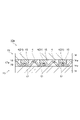
- FIG. 1 is a diagram schematically showing a vertical cross section of an adhesive film for circuit connection (hereinafter, also simply referred to as “adhesive film”) of one embodiment.
- the adhesive film 1a shown in FIG. 1 includes a first adhesive layer 2 containing conductive particles 4 and an adhesive component 5, and a second adhesive layer 3 provided on the first adhesive layer 2.
- the conductive particles 4 are present in the vertical cross section of the adhesive film 1a so as to be arranged in the horizontal direction (left-right direction in FIG. 1) with adjacent conductive particles separated from each other.
- the "longitudinal cross section” means a cross section (cross section in the stacking direction) substantially orthogonal to the main surface (for example, the main surface of the adhesive film 1a).
- the adhesive film 1a is an adhesive film for circuit connection.
- for circuit connection means that it is used for connecting circuit members.
- the adhesive film 1a is interposed between, for example, a first circuit member having a first electrode and a second circuit member having a second electrode, and is interposed between the first circuit member and the second circuit member. Is hot-bonded to be used to electrically connect the first electrode and the second electrode to each other via conductive particles.
- the adhesive film 1a may or may not have anisotropic conductivity. That is, the adhesive film 1a may be an anisotropically conductive adhesive film or a non-anisotropically conductive (for example, isotropically conductive) adhesive film.
- FIG. 2 is an enlarged view of a main part of the adhesive film 1a shown in FIG.
- the adhesive film 1a includes a region (existing region) R1 in which the conductive particles 4 are present and R2 in which the conductive particles 4 are not present (absent region) when the vertical cross section thereof is viewed.
- the first adhesive layer 2 is configured so that the first adhesive component 5, the conductive particles 4, and the first adhesive component 5 are arranged in this order in the stacking direction.
- a second adhesive layer 3 is laminated on the adhesive layer 3. That is, the first adhesive component 5 is present between the surface 2a of the first adhesive layer 2 opposite to the second adhesive layer 3 and the conductive particles 4, and the conductive particles.
- the first adhesive component 5 is also present on the surface of the fourth adhesive layer 3 on the side of the second adhesive layer 3 so as to cover the surface.
- the shortest distance D from the surface 2a of the first adhesive layer 2 opposite to the second adhesive layer 3 to the surface of the conductive particles 4 suppresses an increase in connection resistance in a high temperature and high humidity environment, and makes a circuit connection. From the viewpoint of suppressing the flow of conductive particles at the time (during thermocompression bonding), it may be more than 0 ⁇ m and not more than 1 ⁇ m. From the same viewpoint, the shortest distance D may be 0.1 ⁇ m or more, 0.2 ⁇ m or more, or 0.8 ⁇ m or less.
- the shortest distance d11 from the interface S of the first adhesive layer 2 and the second adhesive layer 3 to the surface of the conductive particles 4 may be, for example, 0.1 ⁇ m or more, 3.0 ⁇ m or less, 2.0 ⁇ m or less. It may be less than or equal to or less than 1.0 ⁇ m.
- the first adhesive component 5 may not be present on the surface of the conductive particles 4 on the second adhesive layer 3 side. That is, it can be said that the shortest distance d11 may be 0 ⁇ m or more.
- the shortest distance d21 from the interface S of the first adhesive layer 2 and the second adhesive layer 3 to the surface 3a of the second adhesive layer 3 opposite to the first adhesive layer 2 in the existing region R1. May be, for example, 3.0 ⁇ m or more, 5.0 ⁇ m or more, or 10.0 ⁇ m or more, and may be 50 ⁇ m or less.
- the first adhesive component 5 exists so as to cover the surface of the conductive particles 4 (including the surface on the second adhesive layer 3 side), the first adhesive layer 2 and The interface S of the second adhesive layer 3 has a curved surface that follows the surface shape of the conductive particles 4 in the vicinity of the conductive particles 4 in the non-existent region R2, and the first is as the distance from the conductive particles 4 increases.
- the surface 2a on the opposite side of the adhesive layer 2 from the second adhesive layer 3 and the surface 3a on the opposite side to the first adhesive layer 2 of the second adhesive layer 3 are substantially parallel to each other. Become.
- the thickness of the first adhesive layer 2 is the thickest in the vicinity of the conductive particles 4, and becomes thinner as the distance from the conductive particles 4 increases.
- the thickness of the second adhesive layer 3 is the thinnest in the vicinity of the conductive particles 4, and becomes thicker as the distance from the conductive particles 4 increases.
- the thickness of the first adhesive layer 2 and the thickness of the second adhesive layer 3 are the thickness of the first adhesive layer 2 in the absent region R2 in which the conductive particles 4 do not exist and the thickness of the second adhesive layer 3. Each is defined as the thickness of the second adhesive layer 3. Further, a preferable range of the thickness of the first adhesive layer 2 and the thickness of the second adhesive layer 3 will be described below, but the following describes the first adhesion at an arbitrary position of the absent region R2.
- the thickness of the agent layer 2 (for example, both the thickness d12 in the vicinity of the conductive particles 4 and the thickness d13 at a position away from the conductive particles 4) and the thickness of the second adhesive layer 3 (for example, in the vicinity of the conductive particles 4). It means that the thickness d22 and the thickness d23 at a position away from the thickness d22) may be within the range shown below.
- the thickness of the first adhesive layer 2 is smaller than the average particle size of the conductive particles 4. Specifically, the thickness of the first adhesive layer 2 makes it easier for the conductive particles 4 to be captured between the electrodes facing each other, and from the viewpoint of further reducing the connection resistance, the average particle size of the conductive particles 4 is 0. It may be 6 times or more, 0.7 times or more, or 0.8 times or more. The thickness of the first adhesive layer 2 is such that when the conductive particles are sandwiched between the electrodes facing each other during thermal pressure bonding, the conductive particles are more easily crushed and the connection resistance can be further reduced. It may be less than 1.0 times, 0.9 times or less, or 0.8 times or less the average particle size. From these viewpoints, the thickness of the first adhesive layer 2 is 0.6 times or more and less than 1.0 times, 0.7 to 0.9 times, 0.7 to 0 times the average particle size of the conductive particles 4. It may be 0.8 times or 0.8 to 0.9 times.
- the ratio of the thickness of the second adhesive layer 3 to the total thickness of the first adhesive layer 2 and the second adhesive layer 3 may be less than 96% from the viewpoint of suppressing the flow of the conductive particles 4 at the time of circuit connection (during thermal pressure bonding).
- the above ratio may be 94% or less, 93% or less, 88% or less, or 86% or less from the viewpoint of further suppressing the flow of the conductive particles 4 at the time of circuit connection (thermocompression bonding).
- the above ratio may be, for example, 75% or more, 78% or more, or 80% or more.
- the thickness of the first adhesive layer 2 may be, for example, 1.0 ⁇ m or more, 2.0 ⁇ m or more, or 3.0 ⁇ m or more from the viewpoint of being able to capture conductive particles more efficiently. It may be 0 ⁇ m or less, 5.0 ⁇ m or less, or 4.0 ⁇ m or less, and may be 1.0 to 6.0 ⁇ m, 2.0 to 5.0 ⁇ m, or 3.0 to 4.0 ⁇ m.
- the thickness of the second adhesive layer 3 is 5.0 ⁇ m or more and 8.0 ⁇ m from the viewpoint that the space between the electrodes can be sufficiently filled to seal the electrodes and better reliability can be obtained. It may be 15.0 ⁇ m or more or 10.0 ⁇ m or more, 15.0 ⁇ m or less, 13.0 ⁇ m or less, 12.0 ⁇ m or less, 11.0 ⁇ m or less, or 8.0 ⁇ m or less, 5.0 to 15.0 ⁇ m, 8. It may be 0 to 13.0 ⁇ m, 10.0 to 11.0 ⁇ m, 6.0 to 8.0 ⁇ m, 9.0 to 11.0 ⁇ m or 10.0 to 12.0 ⁇ m.
- the total thickness of the first adhesive layer 2 and the second adhesive layer 3 is, for example, 6.0 ⁇ m or more, 8.0 ⁇ m or more, 10.0 ⁇ m or more, and 12.0 ⁇ m. It may be more than or equal to 14.0 ⁇ m, and may be 18.0 ⁇ m or less, 16.0 ⁇ m or less, 14.0 ⁇ m or less, or 10.0 ⁇ m or less, 6.0 to 18.0 ⁇ m, 8.0 to 16.0 ⁇ m. It may be 10.0 to 14.0 ⁇ m, 8.0 to 10.0 ⁇ m, 12.0 to 14.0 ⁇ m or 14.0 to 16.0 ⁇ m.
- the thickness of the first adhesive layer 2 and the thickness of the second adhesive layer 3 described above are, for example, a bisphenol A type epoxy resin obtained by sandwiching an adhesive film between two sheets of glass (thickness: about 1 mm).
- a resin composition consisting of 100 g (trade name: JER811, manufactured by Mitsubishi Chemical Co., Ltd.) and 10 g of a curing agent (trade name: Epomount curing agent, manufactured by Refine Tech Co., Ltd.) is cast and then cross-sectionald using a polishing machine. It can be obtained by polishing and measuring using a scanning electron microscope (SEM, trade name: SU-8000, manufactured by Hitachi High-Tech Science Co., Ltd.).
- the first adhesive layer 2 has a flow rate of 130 to 250%.
- the flow rate is an index indicating the fluidity (flow) at the time of thermocompression bonding, and specifically, it is measured by the following methods (A1) to (A4).
- A1 The adhesive film 1a is punched in the thickness direction with the base material attached on both main surfaces of the adhesive film 1a, and a circle having a diameter R (unit: mm) of 0.1 to 1 mm. Obtain a plate-shaped evaluation adhesive film.
- A2 After peeling the base material on the first adhesive layer side from the evaluation adhesive film, the evaluation adhesive film is applied from the first adhesive layer side to a glass plate having a thickness of 0.15 mm (first).
- a glass plate (second glass plate) having a thickness of 0.15 mm is placed on the second adhesive layer, and the pressure bonding temperature is 170 ° C., the pressure bonding pressure is 80 MPa, and the pressure bonding is performed. Thermocompression bonding is performed under the condition of time 5s to obtain a pressure-bonded body.
- an evaluation adhesive film having a diameter R (unit: mm) of 0.1 to 1 mm is obtained.
- the diameter R (unit: mm) may be 1 mm, and when the width of the adhesive film 1a is less than 1 mm, the adhesive film 1a
- the diameter R may be adjusted according to the width.
- the above steps do not prevent the adhesive film 1a from having a disk shape of 0.1 to 1 mm.
- the details of the evaluation method are shown in Examples.
- the second adhesive layer 3 may have a minimum melt viscosity of, for example, 200 to 4000 Pa ⁇ s.
- the minimum melt viscosity of the second adhesive layer 3 may be less than 200 Pa ⁇ s, but when the minimum melt viscosity of the second adhesive layer 3 is 200 Pa ⁇ s or more, the flow of conductive particles due to resin flow. Is suppressed, and conductive particles tend to be easily captured between the electrodes.
- the minimum melt viscosity of the second adhesive layer 3 may be larger than 4000 Pa ⁇ s, but when the minimum melt viscosity of the second adhesive layer 3 is 4000 Pa ⁇ s or less, better resin exclusion property is obtained. And the connection resistance tends to be lower.
- the minimum melt viscosity of the second adhesive layer 3 may be 500 Pa ⁇ s or more or 800 Pa ⁇ s or more, 3000 Pa ⁇ s or less, 2500 Pa ⁇ s or less, 2000 Pa ⁇ s or less, or 1500 Pa ⁇ s. It may be less than or equal to 500 to 2500 Pa ⁇ s or 800 to 1500 Pa ⁇ s.
- the minimum melt viscosity of the second adhesive layer 3 can be measured by the method described in Examples.
- the temperature at which the minimum melt viscosity of the second adhesive layer 3 is reached may be, for example, 50 to 100 ° C.
- the minimum melt viscosity reaching temperature of the second adhesive layer 3 may be less than 50 ° C., but when the minimum melt viscosity reaching temperature of the second adhesive layer 3 is 50 ° C. or higher, the storage stability of the film is stable. Also tends to be improved, and hardening during temporary crimping tends to be suppressed.
- the temperature at which the minimum melt viscosity of the second adhesive layer 3 is reached may be higher than 100 ° C., but when the temperature at which the minimum melt viscosity of the second adhesive layer 3 is reached is 100 ° C. or lower, the temperature is 130 to 180 ° C.
- the minimum melt viscosity reaching temperature of the second adhesive layer 3 may be 60 ° C. or higher, 70 ° C. or higher, or 75 ° C. or higher, and 90 ° C. or lower, 85 ° C. or lower, or 80 ° C. or lower. It may be 60 to 90 ° C, 70 to 90 ° C, 75 to 85 ° C or 75 to 80 ° C.
- the first adhesive layer 2 is, for example, conductive particles 4 (hereinafter, may be referred to as “(A) component”) and a thermosetting component (hereinafter, may be referred to as “(B) component”). And a cured product (photo-cured product) of a photocurable component (hereinafter, may be referred to as “(C) component”).
- the component (B) is a component that can flow at the time of connection, and is, for example, an uncured curable component (for example, a resin component).
- the cured product of the component (C) may be a cured product obtained by completely curing the component (C), or may be a cured product obtained by curing a part of the component (C).
- the first adhesive layer 2 does not have to contain the cured product of the component (C).
- the components other than the component (A) constituting the first adhesive layer 2 are, for example, non-conductive components (for example, an insulating resin component).
- the component (A) is not particularly limited as long as it is conductive particles, such as metal particles made of metal such as Au, Ag, Ni, Cu, and solder, and conductive carbon particles made of conductive carbon. May be.
- the component (A) may be a coated conductive particle containing a nucleus containing non-conductive glass, ceramic, plastic (polystyrene, etc.) and the like, and a coating layer containing the metal or conductive carbon and covering the nucleus. good.
- coated conductive particles including metal particles formed of a heat-meltable metal or a nucleus containing plastic and a coating layer containing metal or conductive carbon and covering the nucleus is used.
- the adhesive layer can be easily deformed by heating or pressurizing. Therefore, when the electrodes are electrically connected to each other, the contact area between the electrodes and the component (A) can be increased, and the conductivity between the electrodes can be further improved.
- the component (A) may be an insulating coated conductive particle including the above-mentioned metal particles, conductive carbon particles, or coated conductive particles and an insulating material such as a resin and having an insulating layer covering the surface of the particles. good.
- the component (A) is an insulating coated conductive particle, even when the content of the component (A) is large, the surface of the particle is coated with the resin, so that the component (A) is short-circuited due to contact with each other. The generation can be suppressed, and the insulation between adjacent electrode circuits can be improved.
- one of the above-mentioned various conductive particles may be used alone or in combination of two or more.
- the maximum particle size of the component (A) is smaller than the minimum distance between the electrodes (the shortest distance between adjacent electrodes).
- the maximum particle size of the component (A) may be 2.5 ⁇ m or more, 3.0 ⁇ m or more, or 3.5 ⁇ m or more from the viewpoint of excellent dispersibility and conductivity.
- the maximum particle size of the component (A) may be 6.0 ⁇ m or less, 5.0 ⁇ m or less, 4.5 ⁇ m or less, or 4.0 ⁇ m from the viewpoint of excellent dispersibility and conductivity. It may be: From these viewpoints, the maximum particle size of the component (A) may be 2.5 to 6.0 ⁇ m, 3.0 to 5.0 ⁇ m, or 3.0 to 4.0 ⁇ m. , 3.5-4.5 ⁇ m.
- the particle size of any 300 conductive particles (pcs) is measured by observation using a scanning electron microscope (SEM), and the largest value obtained is the maximum particle size of the component (A). And.
- the particle size of the component (A) is the diameter of a circle circumscribing the conductive particles in the SEM image.
- the average particle size of the component (A) may be 2.5 ⁇ m or more, 3.0 ⁇ m or more, or 3.5 ⁇ m or more from the viewpoint of excellent dispersibility and conductivity.
- the average particle size of the component (A) may be 6.0 ⁇ m or less, 5.0 ⁇ m or less, 4.5 ⁇ m or less, or 4.0 ⁇ m from the viewpoint of excellent dispersibility and conductivity. It may be: From these viewpoints, the average particle size of the component (A) may be 2.5 to 6.0 ⁇ m, 3.0 to 5.0 ⁇ m, or 3.0 to 4.0 ⁇ m. , 3.5-4.5 ⁇ m.
- the particle size of any 300 conductive particles is measured by observation using a scanning electron microscope (SEM), and the average value of the obtained particle sizes is taken as the average particle size.
- the particle density of the component (A) in the first adhesive layer 2 may be 5000 pieces / mm 2 or more, and may be 10000 pieces / mm 2 or more, from the viewpoint that stable connection resistance can be easily obtained. It may be 20000 pieces / mm 2 or more.
- the particle density of the component (A) in the first adhesive layer 2 may be 50,000 pieces / mm 2 or less, and 40,000 pieces / mm 2 or less, from the viewpoint of improving the insulating property between adjacent electrodes. It may be 30,000 pieces / mm 2 or less. From these viewpoints, the particle density of the component (A) may be 5000 to 50,000 pieces / mm 2 , 10,000 to 40,000 pieces / mm 2 or 20,000 to 30,000 pieces / mm 2 .
- the content of the component (A) is, for example, 5% by mass or more, 15% by mass or more, or 20% by mass or more based on the total mass of the first adhesive layer from the viewpoint of further improving the conductivity. It may be there.
- the content of the component (A) may be, for example, 50% by mass or less, 40% by mass or less, or 30% by mass or less based on the total mass of the first adhesive layer from the viewpoint of easily suppressing a short circuit. From these viewpoints, the content of the component (A) may be, for example, 5 to 50% by mass, 10 to 40% by mass, or 20 to 30% by mass based on the total mass of the first adhesive layer.
- the content of the component (A) in the composition for forming the first adhesive layer 2 (the first adhesive composition described later) (based on the total mass of the composition) is the same as the above range. It may be there.
- the component (B) is not particularly limited as long as it is a component that is cured by heat.
- the component (B) is, for example, a resin component, and is a thermosetting compound (hereinafter, may be referred to as “(B1) component”) and a curing agent for the thermosetting compound (hereinafter, “(B2)). It may be referred to as "ingredient").
- Thermosetting compound The component (B1) is a compound that reacts and crosslinks by heating in the coexistence with the component (B2).
- the component (B1) may be, for example, a radically polymerizable compound (hereinafter, may be referred to as “(B1-1) component”) and a cationically polymerizable compound (hereinafter, referred to as “(B1-2) component”). In some cases).
- a radically polymerizable compound hereinafter, may be referred to as “(B1-1) component”
- (B1-2) component a cationically polymerizable compound
- As the component (B1) one type may be used alone, or a plurality of types may be used in combination.
- Component (B1-1) Radical Polymerizable Compound
- the component (B1-1) has at least one radically polymerizable group.
- the radically polymerizable group include a (meth) acryloyl group, a vinyl group, an allyl group, a styryl group, an alkenyl group, an alkenylene group, a maleimide group and the like.
- the number of radically polymerizable groups (number of functional groups) of the component (B1) is 2 or more from the viewpoint that the desired melt viscosity can be easily obtained after polymerization, the effect of reducing the connection resistance is further improved, and the connection reliability is superior. It may be 10 or less from the viewpoint of suppressing curing shrinkage during polymerization. Further, in order to balance the crosslink density and the curing shrinkage, in addition to the compound having the number of radically polymerizable groups within the above range, a compound having the number of radically polymerizable groups outside the above range may be used. good
- the component (B1-1) may contain a (meth) acrylate compound as a radically polymerizable compound from the viewpoint of suppressing the flow of conductive particles.
- the (meth) aclate compound may be a monofunctional (meth) acrylate having one (meth) acryloyl group, or may be a polyfunctional (meth) acrylate having two or more (meth) acryloyl groups. , These may be used together.
- the component (B1-1) may be a polyfunctional (meth) acrylate from the viewpoint of further suppressing the flow of conductive particles.
- Examples of the monofunctional (meth) acrylate include (meth) acrylic acid; methyl (meth) acrylate, ethyl (meth) acrylate, butyl (meth) acrylate, isobutyl (meth) acrylate, and tert-butyl (meth) acrylate.
- examples thereof include (meth) acrylate having an oxetanyl group such as (3-ethyloxetane-3-yl) methyl (meth) acrylate.
- polyfunctional (meth) acrylate examples include ethylene glycol di (meth) acrylate, diethylene glycol di (meth) acrylate, triethylene glycol di (meth) acrylate, tetraethylene glycol di (meth) acrylate, and polyethylene glycol di (meth) acrylate.
- the content of the monofunctional (meth) acrylate may be, for example, 0 to 60% by mass, 0 to 50% by mass, or 0 to 40% by mass based on the total mass of the component (B1-1).
- the content of the polyfunctional (bifunctional or higher) (meth) acrylate is, for example, 40, based on the total mass of the component (B1-1), from the viewpoint of achieving both the effect of reducing the connection resistance and the suppression of particle flow. It may be up to 100% by mass, 50 to 100% by mass, or 60 to 100% by mass.
- the component (B1-1) may be an epoxy (meth) acrylate from the viewpoint that a first adhesive layer having a flow rate of 250% or less can be easily obtained. From the same viewpoint, the component (B1-1) may be an aromatic epoxy (meth) acrylate as described above.
- the content of the epoxy (meth) acrylate may be, for example, 40 to 100% by mass, 50 to 100% by mass, or 60 to 100% by mass based on the total mass of the component (B1-1).
- the component (B1-1) has a tricyclodecane structure, a crosslinked structure such as norbornane structure, and / or an aromatic structure from the viewpoint that a first adhesive layer having a flow rate of 250% or less can be easily obtained. You can do it.
- a (meth) acrylate having a tricyclodecane structure, a crosslinked structure such as norbornane structure, and / or an aromatic structure is used as the component (B1-1), the first adhesive having a flow rate of 250% or less. Layers are easier to obtain.
- the content of the (meth) acrylate having a tricyclodecane structure, a crosslinked structure such as norbornane structure, and / or an aromatic structure is, for example, 40 to 100% by mass based on the total mass of the component (B1-1). , 50-100% by mass or 60-100% by mass.
- the component (B1-1) may contain a compound having a weight average molecular weight of 300 to 4000 from the viewpoint that a first adhesive layer having a flow rate of 130 to 250% can be easily obtained.
- the content of the compound having a weight average molecular weight of 300 to 4000 may be, for example, 20% by mass or more, 30% by mass or more, or 40% by mass or more, based on the total mass of the component (B1-1), 100. It may be 0% by mass or less, 80% by mass or less, or 60% by mass or less, and may be 20 to 100% by mass, 30 to 80% by mass, or 40 to 60% by mass.
- the weight average molecular weight of all (B1-1) components may be 300 to 4000.
- the weight average molecular weight in the present specification means a value measured by a gel permeation chromatograph (GPC) using a calibration curve using standard polystyrene.
- the component (B1-1) may contain other radically polymerizable compounds in addition to the (meth) acrylate compound.
- examples of other radically polymerizable compounds include maleimide compounds, vinyl ether compounds, allyl compounds, styrene derivatives, acrylamide derivatives, nadiimide derivatives and the like.
- the content of the other radically polymerizable compound may be, for example, 0 to 40% by mass based on the total mass of the component (B1).
- Component (B1-2) Cationicly polymerizable compound
- the component (B1-2) may be a compound having a cyclic ether group from the viewpoint of further improving the effect of reducing the connection resistance and improving the connection reliability.
- the effect of reducing the connection resistance tends to be further improved.
- the component (B1-2) may be a compound having a plurality of cyclic ether groups.
- the epoxy compound is a compound having an epoxy group, for example, having two or more epoxy groups in one molecule.
- Epoxy compounds include an epoxy resin derived from bisphenol A and epichlorohydrin (bisphenol A type epoxy resin) and an epoxy compound having an alicyclic epoxy group (3', 4'-epoxycyclohexylmethyl-3,4. -Epoxycyclohexanecarboxylate, etc.) can be used.
- an epoxy compound having an alicyclic epoxy group it is easy to obtain a first adhesive layer having a flow rate of 250% or less. From the viewpoint that a first adhesive layer having a flow rate of 130 to 250% can be easily obtained, the functional group equivalent of the epoxy compound may be 100 to 500 g / eq.
- Examples of commercially available epoxy compounds include YL-980 (trade name, manufactured by Mitsubishi Chemical Co., Ltd.), jER1007 (trade name, manufactured by Mitsubishi Chemical Co., Ltd.), which is a bisphenol A type epoxy resin, and an alicyclic epoxy compound.
- Examples thereof include EHPE3150, EHPE3150CE, CEL (celloxide) 8010, CEL (celloxide) 2021P, CEL (celloxside) 2081 (trade name, manufactured by Daicel Co., Ltd.). These may use one kind of compound alone or may use a plurality of kinds in combination.
- the oxetane compound is a compound having an oxetaneyl group, for example, having two or more oxetanel groups in one molecule.
- the functional group equivalent of the oxetane compound may be 100 to 500 g / eq.
- the oxetane compound may be used in combination with an epoxy compound having an alicyclic epoxy group. In this case, it becomes easier to obtain a first adhesive layer having a flow rate of 250% or less.
- Examples of commercially available oxetane compounds include ETERNACOLL OXBP (trade name, 4,4'-bis [(3-ethyl-3-oxetanyl) methoxymethyl] biphenyl, manufactured by Ube Kosan Co., Ltd.), OXSQ, OXT-121, and the like. Examples thereof include OXT-221, OXT-101, and OXT-212 (trade name, manufactured by Toagosei Corporation). These may use one kind of compound alone or may use a plurality of kinds in combination.
- Component (B2) Curing agent of component (B1)
- the component (B2) is, for example, a thermal polymerization initiator.
- the component (B2) may be, for example, a thermal radical generator (hereinafter, may be referred to as “(B2-1) component”) and a thermal acid generator (hereinafter, referred to as “(B2-2) component”). In some cases).
- the component (B2) may be selected according to the type of the component (B1).
- a thermal radical generator thermal radical polymerization initiator
- a thermal acid generator thermal cation polymerization initiator
- Component (B2-1) Thermal radical generator
- the component (B2-1) is decomposed by heat to generate free radicals. That is, the component (B2-1) is a compound that generates radicals by applying thermal energy from the outside.
- the component (B2-1) can be arbitrarily selected from conventionally known organic peroxides and azo compounds.
- the component (B2-1) may be an organic peroxide from the viewpoint of further improving the effect of suppressing the flow of conductive particles and the effect of suppressing peeling after transfer, and is more stable, reactive and compatible. From a good viewpoint, it may be an organic peroxide having a 1-minute half-life temperature of 90 to 175 ° C. and a weight average molecular weight of 180 to 1000.
- the 1-minute half-life temperature of the organic peroxide is within the above range, the storage stability tends to be further excellent, and a sufficiently high radical polymerizable property can be obtained, so that the organic peroxide can be cured in a short time.
- the 1-minute half-life temperature of the component (B2-1) is 90 to 175 ° C., it becomes easy to obtain a first adhesive layer having a flow rate of 250% or less.
- component (B2-1) examples include 1,1,3,3-tetramethylbutylperoxyneodecanoate, di (4-t-butylcyclohexyl) peroxydicarbonate, and di (2-ethylhexyl).
- the content of the component (B2-1) is, for example, (B1-1) from the viewpoint of excellent quick-curing property, and further improving the effect of suppressing the flow of conductive particles and the effect of suppressing exfoliation after transfer.
- it may be 0.1 to 20 parts by mass, 1 to 18 parts by mass, 3 to 15 parts by mass, or 5 to 12 parts by mass with respect to 100 parts by mass of the component.
- the (B2-2) component is a thermal polymerization initiator (thermal latent cation generator) that generates an acid or the like by heating to initiate polymerization.
- the component (B2-2) may be a salt compound composed of a cation and an anion.
- Examples thereof include onium salts such as sulfonium salts, phosphonium salts, ammonium salts, diazonium salts, iodonium salts and anilinium salts having anions such as SbF 6 ⁇ and AsF 6 ⁇ . These may be used individually by 1 type, and may be used in combination of a plurality of types.
- the component (B2-2) may be, for example, a salt compound having an anion containing boron as a constituent element from the viewpoint of quick curing.
- a salt compound having BF 4- or BR 4- R indicates a phenyl group substituted with two or more fluorine atoms or two or more trifluoromethyl groups). Be done.
- the anion containing boron as a constituent element may be BR 4- , and more specifically, tetrakis (pentafluorophenyl) borate.
- the component (B2-2) may be a sulfonium salt or an ammonium salt from the viewpoint of storage stability.
- the sulfonium salt may be, for example, a salt compound having a cation represented by the following formula (I).
- R 5 and R 6 each independently represent a hydrogen atom, an alkyl group having 1 to 20 carbon atoms, or an organic group containing a substituent or an unsubstituted aromatic hydrocarbon group.
- R 7 represent an alkyl group having 1 to 6 carbon atoms.
- the salt compound having a cation represented by the formula (I) may be an aromatic sulfonium salt compound from the viewpoint of achieving both storage stability and low temperature activity. That is, at least one of R5 and R6 in the formula (I) may be an organic group having a substituent or containing an unsubstituted aromatic hydrocarbon group.
- the anion in the salt compound having a cation represented by the formula (I) may be an anion containing antimony as a constituent element, and may be, for example, hexafluoroantimonate (hexafluoroantimonic acid).
- Specific examples of the compound having a cation represented by the formula (I) include 1-naphthylmethyl-p-hydroxyphenylsulfonium hexafluoroantimonate (manufactured by Sanshin Chemical Co., Ltd., SI-60 main agent).
- the ammonium salt may be, for example, a salt compound having a cation represented by the following formula (II).
- R 8 and R 9 each independently represent a hydrogen atom, an alkyl group having 1 to 20 carbon atoms, or an organic group containing a substituent or an unsubstituted aromatic hydrocarbon group.
- R 10 and R 11 each independently represent an alkyl group having 1 to 6 carbon atoms.
- the salt compound having a cation represented by the formula (II) may be, for example, an anilinium salt compound because it has resistance to a substance that can cause curing inhibition to cation curing. That is, at least one of R 8 and R 9 in the formula (II) may be an organic group having a substituent or containing an unsubstituted aromatic hydrocarbon group.
- the anilinium salt compound include N, N-dialkylanilinium salts such as N, N-dimethylanilinium salt and N, N-diethylanilinium salt.
- the anion in the salt compound having a cation represented by the formula (II) may be an anion containing boron as a constituent element, and may be, for example, tetrakis (pentafluorophenyl) borate.
- the compound having a cation represented by the formula (II) may be an anilinium salt having an anion containing boron as a constituent element.
- anilinium salt compounds include CXC-1821 (trade name, manufactured by King Industries) and the like.
- the content of the component (B2-2) is based on 100 parts by mass of the component (B1-2) from the viewpoint of ensuring the formability and curability of the adhesive film for forming the first adhesive layer.
- it may be 0.1 to 20 parts by mass, 1 to 18 parts by mass, 3 to 15 parts by mass, or 5 to 12 parts by mass.
- the component (B) is not limited to the combination of the component (B1) and the component (B2).
- the component (B1) contains the above-mentioned epoxy compound and / or oxetane compound
- a known amine-based curing agent or imidazole-based curing agent may be used as the component (B2).
- the content of the component (B) is the adhesive component (first adhesive layer) in the first adhesive layer from the viewpoint of ensuring the curability of the adhesive film for forming the first adhesive layer. Based on the total amount of the components (components other than the component (A)) in the mixture, for example, it may be 5% by mass or more, 10% by mass or more, 15% by mass or more, or 20% by mass or more.
- the content of the component (B) is the adhesive component (first adhesive layer) in the first adhesive layer from the viewpoint of ensuring the formability of the adhesive film for forming the first adhesive layer.
- the content of the component (B) is, for example, based on the total amount of the adhesive components (components other than the component (A) in the first adhesive layer) in the first adhesive layer. It may be 5 to 70% by mass, 10 to 60% by mass, 15 to 50% by mass, or 20 to 40% by mass.
- the content of the component (B) in the composition for forming the first adhesive layer 2 (the first adhesive composition described later) (based on the total amount of the adhesive components in the composition) is It may be the same as the above range.
- the component (C) is not particularly limited as long as it is a component that is cured by light.
- the component (C) is, for example, a resin component, and is a photocurable compound (hereinafter, may be referred to as “(C1) component”) and a curing agent for the photocurable compound (hereinafter, “(C2)). It may be referred to as "ingredient").
- the cured product of the component (C) has a thermosetting property
- the cured product does not correspond to the component (B).
- Component (C1) Photocurable compound
- the component (C1) is a compound that reacts and crosslinks by irradiating with light in the coexistence with the component (C2).
- the component (C1) may be, for example, a radically polymerizable compound (hereinafter, may be referred to as “(C1-1) component”) and a cationically polymerizable compound (hereinafter, referred to as “(C1-2) component”). In some cases).
- the component (C1) is a compound having a radically polymerizable group and a cationically polymerizable group such as a (meth) acrylate having an epoxy group and a (meth) acrylate having an oxetanyl group ((C1-1) component and (C1-2). It may be a compound corresponding to both of the components).
- the component (C1-1) the compound described in detail as the component (B1-1) can be used, and the details (preferable aspects for setting the content ratio and the flow rate to 130 to 250%, etc.) are (B1). -1) It is the same as the case of the component.
- the compound described in detail as the component (B1-2) can be used, and the details thereof (content ratio, preferred embodiment for setting the flow rate to 130 to 250%, etc.). Is the same as in the case of the (B1-2) component.
- the component (C1) one type may be used alone, or a plurality of types may be used in combination.
- Component (C2) Curing agent of component (C1)
- the component (C2) is, for example, a photopolymerization initiator.
- the component (C2) may be, for example, a photoradical generator (hereinafter, may be referred to as “(C2-1) component”) and a photoacid generator (hereinafter, referred to as “(C2-2) component”). In some cases).
- the component (C2) may be selected according to the type of the component (C1).
- a photoradical generator photoradical polymerization initiator
- the component (C1) is a cationically polymerizable compound, (C2).
- a photoacid generator (photocationic polymerization initiator) may be used as a component.
- the component (C2) is a component that does not function as a curing agent for the component (B1).
- the component (C2) is a compound that does not generate radicals by light (for example, a photocationic polymerization initiator)
- the component (B) is a cationically polymerizable compound.
- (C2) component is a compound that does not generate a cation by light (for example, a photoradical polymerization initiator).
- the (C2-1) component is light containing a wavelength in the range of 150 to 750 nm, preferably light containing a wavelength in the range of 254 to 405 nm, and more preferably light containing a wavelength in the range of 254 to 405 nm. It is a photopolymerization initiator that generates radicals by irradiation with light containing a wavelength (for example, ultraviolet light).
- a wavelength for example, ultraviolet light.
- the component (C2-1) one type may be used alone, or a plurality of types may be used in combination.
- the (C2-1) component is decomposed by light to generate free radicals. That is, the component (C2-1) is a compound that generates radicals by applying light energy from the outside.
- the component (C2-1) is an oxime ester structure, a bisimidazole structure, an acridine structure, an ⁇ -aminoalkylphenone structure, an aminobenzophenone structure, an N-phenylglycine structure, an acylphosphine oxide structure, a benzyldimethylketal structure, and an ⁇ -hydroxyalkyl. It may be a compound having a structure such as a phenone structure.
- the component (C2-1) is composed of a group consisting of an oxime ester structure, an ⁇ -aminoalkylphenone structure, and an acylphosphine oxide structure from the viewpoint that the desired melt viscosity can be easily obtained and the effect of reducing the connection resistance is superior. It may be a compound having at least one structure selected.
- the compound having an oxime ester structure examples include 1-phenyl-1,2-butandion-2- (o-methoxycarbonyl) oxime and 1-phenyl-1,2-propanedione-2- (o-methoxycarbonyl).
- the compound having an ⁇ -aminoalkylphenone structure include 2-methyl-1- [4- (methylthio) phenyl] -2-morpholinopropane-1-one and 2-benzyl-2-dimethylamino-1. -Morphorinophenyl) -butanone-1 and the like.
- compounds having an acylphosphine oxide structure include bis (2,6-dimethoxybenzoyl) -2,4,4-trimethyl-pentylphosphine oxide and bis (2,4,6, -trimethylbenzoyl) -phenylphosphine.
- examples thereof include oxides, 2,4,6-trimethylbenzoyl-diphenylphosphine oxide and the like.
- the content of the component (C2-1) is 100 parts by mass of the component (C1-1) from the viewpoint of easily obtaining a first adhesive layer having a flow rate of 130 to 250% and suppressing the flow of conductive particles.
- it may be 0.1 to 10 parts by mass, 0.3 to 7 parts by mass, or 0.5 to 5 parts by mass.
- the (C2-2) component is light containing a wavelength in the range of 150 to 750 nm, preferably light containing a wavelength in the range of 254 to 405 nm, and more preferably light containing a wavelength in the range of 254 to 405 nm. It is a photopolymerization initiator that generates a cationic species by irradiation with light containing a wavelength (for example, ultraviolet light).
- a wavelength for example, ultraviolet light.
- one type may be used alone, or a plurality of types may be used in combination.
- Examples of the (C2-2) component include onium salts such as aromatic diazonium salt, aromatic sulfonium salt, aliphatic sulfonium salt, aromatic iodonium salt, phosphonium salt, pyridinium salt, and selenonium salt, metal arene complex, and silanol /.
- Examples thereof include complex compounds such as aluminum complexes, benzointosylate, o-nitrobenzyltosylate and the like.
- aromatic sulfonium salts for example, triarylsulfonium salts
- sulfonium salts such as aliphatic sulfonium salts
- iodinenium salts such as aromatic iodinenium salts
- iron-alene complexes have high efficiency of cation species generation. Therefore, good reactivity can be easily obtained.
- the component (C2-2) is an onium salt and the counter anion is hexafluoroantimonate, hexafluorophosphonate, tetrafluoroborate, tetrakis (pentafluorophenyl) borate or the like, better reactivity can be easily obtained. ..
- the component (C2-2) is BF 4- , BR 4- ( R is 2 or more fluorine atoms or 2 or more birds) from the viewpoint that a first adhesive layer having a flow rate of 250% or less can be easily obtained. It indicates a phenyl group substituted with a fluoromethyl group.), A sulfonium salt, a phosphonium salt, an ammonium salt, a diazonium salt, an iodonium salt, an anilinium salt having anions such as PF 6 ⁇ , SbF 6 ⁇ , AsF 6 ⁇ . It's okay.
- component (C2-2) light irradiation or heating of a triarylsilyl peroxide derivative, an acylsilane derivative, an ⁇ -sulfonyloxyketone derivative, an ⁇ -hydroxymethylbenzoin derivative, a nitrobenzyl ester derivative, an ⁇ -sulfonylacetophenone derivative, etc.
- Derivatives that generate organic acids can also be used.
- CPI series manufactured by Sun Apro Co., Ltd. Adecaoptomer SP series manufactured by Asahi Denka Kogyo Co., Ltd., Adeka Opton CP series manufactured by Asahi Denka Kogyo Co., Ltd., Union Carbide Co., Ltd.
- CyracureUVI series manufactured by Cyracure UVI and IRGACURE series manufactured by Ciba Specialty Chemicals are preferably used.
- a known singlet sensitizer or triplet sensitizer typified by anthracene, thioxanthone derivative and the like can be used in combination.
- the content of the component (C2-2) is 100 parts by mass of the component (C1-2) from the viewpoint of easily obtaining a first adhesive layer having a flow rate of 130 to 250% and suppressing the flow of conductive particles.
- it may be 0.1 to 10 parts by mass, 0.3 to 7 parts by mass, or 0.5 to 5 parts by mass.
- the content of the cured product of the component (C) is the entire content of the first adhesive layer from the viewpoint of easily obtaining the first adhesive layer having a flow rate of 130% or more and suppressing the flow of conductive particles. It may be 1% by mass or more, 5% by mass or more, or 10% by mass or more based on the mass.
- the content of the cured product of the component (C) is the content of the first adhesive layer from the viewpoint of easily obtaining the first adhesive layer having a flow rate of 250% or less and from the viewpoint of developing low resistance in low-pressure mounting. Based on the total mass, it may be 50% by mass or less, 40% by mass or less, or 30% by mass or less.
- the content of the cured product of the component (C) is, for example, 1 to 50% by mass, 5 to 40% by mass, or 10 to 30% by mass, based on the total mass of the first adhesive layer. It may be there.
- the content of the component (C) in the composition for forming the first adhesive layer 2 (the first adhesive composition described later) (based on the total mass of the composition) is the same as the above range. It may be there.
- the first adhesive layer 2 may further contain other components in addition to the cured product of the component (A), the component (B) and the component (C).
- other components include a thermoplastic resin (hereinafter, may be referred to as “(D) component”), a coupling agent (hereinafter, may be referred to as “(E) component”), and a filler. (Hereinafter, it may be referred to as "(F) component”.) And the like.
- a resin that functions as a film-forming component can be used.
- the component (D) include phenoxy resin, polyester resin, polyamide resin, polyurethane resin, polyester urethane resin, acrylic rubber, epoxy resin (solid at 25 ° C.) and the like. These may be used individually by 1 type, and may be used in combination of a plurality of types.
- the film formability is improved by using the component (D). Among these, when the component (D) is a phenoxy resin, the film formability is more likely to be improved.
- the weight average molecular weight (Mw) of the component (D) is, for example, 5000 to 200,000 from the viewpoint of easily obtaining a first adhesive layer having a flow rate of 130 to 250% and resin exclusion during mounting. It may be 10,000 to 100,000, 20,000 to 80,000, 40,000 to 70,000 or 40,000 to 60,000.
- Mw means a value measured by gel permeation chromatography (GPC) and converted using the calibration curve by standard polystyrene.
- the glass transition temperature Tg of the component (D) may be, for example, 80 to 160 ° C. from the viewpoint that a first adhesive layer having a flow rate of 130 to 250% can be easily obtained.
- the glass transition temperature Tg of the component (D) is a value measured using a differential scanning calorimeter (DSC). Specifically, for example, using DSC, differential scanning calorimetry from room temperature (25 ° C.) to 270 ° C. is performed for two cycles at a heating rate of 10 ° C./min, and Tg is performed from the baseline shift in the second cycle. Can be asked.
- DSC differential scanning calorimeter
- the elastic modulus of the component (D) at room temperature (25 ° C.) is, for example, 1.5 to 2.3 GPa from the viewpoint that a first adhesive layer having a flow rate of 130 to 250% can be easily obtained. good.
- the content of the component (D) is such that the first adhesive layer having a flow rate of 130 to 250% can be easily obtained, the film formability, and the resin exclusion property at the time of mounting. Based on the total mass of the agent layer, it may be 1% by mass or more, 5% by mass or more, 10% by mass or more or 20% by mass or more, and 70% by mass or less, 60% by mass or less, 50% by mass or less or 40% by mass. It may be less than or equal to%.
- the content of the component (D) in the composition for forming the first adhesive layer 2 (the first adhesive composition described later) (based on the total mass of the composition) is the same as the above range. It may be there.
- the ratio of the content of the component (B) to the content of the component (D) is, for example, 0.8 to 0.95 from the viewpoint that a first adhesive layer having a flow rate of 130 to 250% can be easily obtained. May be.
- the component (E) examples include a silane coupling agent having an organic functional group such as a (meth) acryloyl group, a mercapto group, an amino group, an imidazole group and an epoxy group, a silane compound such as tetraalkoxysilane, and a tetraalkoxy titanate derivative. , Polydialkyl titanate derivatives and the like. These may be used individually by 1 type, and may be used in combination of a plurality of types. When the first adhesive layer 2 contains the component (E), the adhesiveness can be further improved.
- the component (E) may be, for example, a silane coupling agent.
- the content of the component (E) may be 0.1 to 10% by mass based on the total mass of the first adhesive layer.
- the content of the component (E) in the composition for forming the first adhesive layer 2 (the first adhesive composition described later) (based on the total mass of the composition) is the same as the above range. It may be there.
- the component (F) include non-conductive fillers (for example, non-conductive particles).
- the component (F) may be either an inorganic filler or an organic filler.
- the inorganic filler include metal oxide fine particles such as silica fine particles, alumina fine particles, silica-alumina fine particles, titania fine particles, and zirconia fine particles; and inorganic fine particles such as metal nitride fine particles.
- the organic filler include organic fine particles such as silicone fine particles, methacrylate / butadiene / styrene fine particles, acrylic / silicone fine particles, polyamide fine particles, and polyimide fine particles. These may be used individually by 1 type, and may be used in combination of a plurality of types.
- the component (F) can be appropriately blended as long as the effect of the present invention is not impaired.
- the first adhesive layer 2 may further contain other additives such as a softener, an accelerator, a deterioration inhibitor, a colorant, a flame retardant, and a thixotropic agent as other components.
- the content (total amount) of the other additives may be, for example, 0.1 to 10% by mass based on the total mass of the first adhesive layer.
- the content of other additives (based on the total mass of the composition) in the composition for forming the first adhesive layer 2 (the first adhesive composition described later) is the same as the above range. It may be there.
- the second adhesive layer 3 contains, for example, a thermosetting component (component (B)).
- component (B) The details of the component (B) are the same as those of the component (B) contained in the first adhesive layer 2.
- the content of the component (B) is 5% by mass or more, 10% by mass or more, 15% by mass or more, or 20% by mass or more based on the total mass of the second adhesive layer from the viewpoint of maintaining reliability. It may be there.
- the content of the component (B) is 70% by mass or less and 60% by mass or less based on the total mass of the second adhesive layer from the viewpoint of preventing the resin seepage problem in the reel, which is one aspect of the supply form. , 50% by mass or less, or 40% by mass or less. From these viewpoints, the content of the component (B) is, for example, 5 to 70% by mass, 10 to 60% by mass, 15 to 50% by mass, or 20 to 40, based on the total mass of the second adhesive layer. It may be% by mass.
- the content of the component (B) in the composition for forming the second adhesive layer 3 (the second adhesive composition described later) (based on the total mass of the composition) is the same as the above range. It may be there.
- the second adhesive layer 3 may further contain a filler (component (F)).
- the details of the component (F) are the same as those of the component (F) contained in the first adhesive layer 2.
- the second adhesive layer 3 contains an inorganic filler as the component (F) from the viewpoint of facilitating the adjustment of fluidity, the viewpoint of improving the elastic modulus after curing, and the viewpoint of lowering the coefficient of linear expansion. good.
- a silica filler such as silica fine particles can be used from the viewpoint of improving reliability.
- the content of silica in the silica filler may be 99% by mass or more, or 100% by mass, based on the total amount of the silica filler.
- the average particle size (primary particle size) of the inorganic filler may be 0.01 ⁇ m or more, 0.03 ⁇ m or more, 0.05 ⁇ m or more, 0.1 ⁇ m or more, or 0.3 ⁇ m or more from the viewpoint of excellent dispersibility.
- the average particle size (primary particle size) of the inorganic filler may be 5.0 ⁇ m or less, 1.0 ⁇ m or less, or 0.5 ⁇ m or less from the viewpoint of excellent dispersibility. From these viewpoints, the average particle size of the inorganic filler is 0.01 to 5.0 ⁇ m, 0.03 to 1.0 ⁇ m, 0.05 to 0.5 ⁇ m, 0.05 to 5.0 ⁇ m, 0.1 to 0. It may be .5 ⁇ m or 0.3-0.5 ⁇ m.
- the content of the inorganic filler may be 20% by mass or more, 30% by mass or more, or 40% by mass or more based on the total mass of the second adhesive layer from the viewpoint of improving the elastic modulus after curing.
- the content of the inorganic filler is 60% by mass or less, 50% by mass or less, or 40% by mass or less based on the total mass of the second adhesive layer from the viewpoint of improving film formation and thermosetting property. It's okay. From these viewpoints, the content of the inorganic filler is 20 to 60% by mass, 30 to 50% by mass, 20 to 40% by mass or 40 to 50% by mass, based on the total mass of the second adhesive layer. It's okay.
- the content of the inorganic filler (based on the total mass of the composition) in the composition for forming the second adhesive layer 3 is the same as the above range. good.
- the second adhesive layer 3 may further contain other components other than the component (F) in the first adhesive layer 2.
- the details of the other components are the same as the details of the other components in the first adhesive layer 2.
- the content of the component (D) may be 1% by mass or more, 5% by mass or more or 10% by mass or more, and 80% by mass or less and 60% by mass or less, based on the total mass of the second adhesive layer. Alternatively, it may be 40% by mass or less.
- the content of the component (D) in the composition for forming the second adhesive layer 3 (the second adhesive composition described later) (based on the total mass of the composition) is the same as the above range. It may be there.
- the content of the component (E) may be 0.1 to 10% by mass based on the total mass of the second adhesive layer.
- the content of the component (E) in the composition for forming the second adhesive layer 3 (the second adhesive composition described later) (based on the total mass of the composition) is the same as the above range. It may be there.
- the content of the other additives may be, for example, 0.1 to 10% by mass based on the total mass of the second adhesive layer.
- the content of other additives (based on the total mass of the composition) in the composition for forming the second adhesive layer 3 (the second adhesive composition described later) is the same as the above range. It may be there.
- the content of the conductive particles (component (A)) in the second adhesive layer 3 is, for example, 1% by mass or less, even if it is 0% by mass, based on the total mass of the second adhesive layer. good. That is, the second adhesive layer 3 does not have to contain the component (A).
- the content of the component (A) in the composition for forming the second adhesive layer 3 (the second adhesive composition described later) (based on the total mass of the composition) is the same as the above range. It may be there.
- the adhesive film 1a is a first adhesive containing, for example, a component (A), a component (B) (a first thermosetting component), and a component (C), and if necessary, other components.
- the step of irradiating the layer made of the composition with light to form the first adhesive layer 2 (first step) and the component (B) component (second) on the first adhesive layer 2 It is manufactured by a method including a step (second step) of laminating a second adhesive layer 3 composed of a second adhesive composition containing a thermosetting component) and, if necessary, other components. Can be done.
- the first step it is not necessary to include the component (C) in the first adhesive composition. In this case, the light irradiation in the first step does not have to be performed.
- the first adhesive composition is dissolved or dispersed by stirring and mixing in an organic solvent, kneading, or the like, and the varnish composition (varnish-like first adhesive) is used.
- Composition is prepared.
- the varnish composition is applied onto the mold-released substrate using a knife coater, roll coater, applicator, comma coater, die coater, etc., and then the organic solvent is volatilized by heating to form the substrate.
- the thickness of the first adhesive layer can be adjusted by adjusting the coating amount of the varnish composition.
- the layer composed of the first adhesive composition is irradiated with light to cure the component (C) in the layer. Let me.
- the first adhesive layer 2 is formed on the base material, and the first adhesive film provided with the first adhesive layer 2 is obtained.
- the organic solvent used in the preparation of the varnish composition is not particularly limited as long as it has the property of being able to dissolve or disperse each component substantially uniformly.
- examples of such an organic solvent include toluene, acetone, methyl ethyl ketone, methyl isobutyl ketone, ethyl acetate, propyl acetate, butyl acetate and the like. These organic solvents can be used alone or in combination of two or more.
- Stirring and mixing or kneading in the preparation of the varnish composition can be carried out by using, for example, a stirrer, a raider, a three-roll, a ball mill, a bead mill, a homodisper or the like.
- the base material is not particularly limited as long as it has heat resistance that can withstand the heating conditions when volatilizing the organic solvent.
- a substrate examples include stretched polypropylene (OPP), polyethylene terephthalate (PET), polyethylene naphthalate, polyethylene isophthalate, polyvinylidene terephthalate, polyolefin, polyacetate, polycarbonate, polyvinylidene sulfide, polyamide, polyimide, cellulose, and the like.
- a substrate (for example, a film) made of an ethylene / vinyl acetate copolymer, polyvinyl chloride, polyvinylidene chloride, a synthetic rubber system, a liquid crystal polymer or the like can be used.
- the heating conditions for volatilizing the organic solvent from the varnish composition applied to the base material can be appropriately set according to the organic solvent to be used and the like.
- the heating conditions may be, for example, 40 to 120 ° C. for 0.1 to 10 minutes.
- a part of the solvent may remain on the first adhesive layer 2 without being removed.
- the content of the solvent in the first adhesive layer 2 may be, for example, 10% by mass or less based on the total mass of the first adhesive layer.
- irradiation light for example, ultraviolet light
- Light irradiation can be performed using, for example, a low-pressure mercury lamp, a medium-pressure mercury lamp, a high-pressure mercury lamp, an ultra-high-pressure mercury lamp, a xenon lamp, a metal halide lamp, an LED light source, or the like.
- the integrated light amount of light irradiation can be appropriately set, but may be, for example, 500 to 3000 mJ / cm 2 .
- the second step is a step of laminating the second adhesive layer 3 on the first adhesive layer 2.
- the base is the same as in the first step except that the second adhesive composition is used instead of the first adhesive composition and the light irradiation is not performed.
- the obtained second adhesive film and the first adhesive film are bonded to each other to form a second adhesive on the first adhesive layer 2.
- the agent layer 3 is laminated.
- Examples of the method of adhering the first adhesive film and the second adhesive film include a method of heat pressing, roll laminating, vacuum laminating and the like. Lamination can be performed, for example, under temperature conditions of 0 to 80 ° C.
- a varnish-like second adhesive composition is applied onto the first adhesive layer 2 and the organic solvent is volatilized to cause a second on the first adhesive layer 2.
- the adhesive layer 3 of the above may be laminated.
- a part of the solvent may remain on the second adhesive layer 3 without being removed.
- the content of the solvent in the second adhesive layer 3 may be, for example, 10% by mass or less based on the total mass of the second adhesive layer.
- the adhesive film 1a described above since the flow rate of the first adhesive layer 2 is 250% or less, it is difficult for conductive particles to flow during thermocompression bonding, and the film of the first adhesive layer after thermocompression bonding is performed. The shape is easy to maintain. Therefore, according to the adhesive film 1a, it is possible to suppress the occurrence of a short circuit due to aggregation of conductive particles. Further, since the adhesive film 1a has a flow rate of 130% or more of the first adhesive layer, the adhesive film 1a is bent during thermocompression bonding, and the bending causes the first adhesive layer to be stretched between the facing electrodes. Adhesive component is reduced.
- the flow rate of the first adhesive layer 2 may be 150% or more, 160% or more, 170% or more or 180% or more, and 230% or less or 200%. It may be 150 to 230% or 180 to 200%.
- the flow rate of the first adhesive layer 2 is, for example, the content of the cured product of the component (A), the component (B) and the component (C), and the components (C1) and (C2) in the component (C). It can be adjusted according to the type and amount of the above, the type and content of any component (particularly the component (D)), and the like.
- the cured product of the component (C) is contained in the first adhesive layer 2, for example, by adjusting the curing rate of the component (C) by adjusting the light irradiation amount, the flow rate in the above range can be easily obtained. It is also possible to obtain the first adhesive layer 2 having the above.
- the flow rate is higher than 250% in the conventional adhesive composition, but the weight average molecular weight of the component (D) is 40,000 or more.
- a thermoplastic resin having a glass transition temperature of 70,000, a glass transition temperature of 80 to 160 ° C., and an elastic modulus of 1.5 to 2.3 GPa at room temperature (25 ° C.) with respect to the content of the component (D).
- the first adhesive layer 2 having a flow rate in the above range can be obtained by a method such as setting the ratio of the content of the components to 0.8 to 0.95.
- circuit connection adhesive film of one embodiment and the method for manufacturing the same have been described above, the circuit connection adhesive film of the present invention is not limited to the above embodiment.
- the circuit connection adhesive film may be composed of three or more layers including layers other than the first adhesive layer 2 and the second adhesive layer 3.
- the adhesive film for circuit connection may be the adhesive film 1b shown in FIG.
- the adhesive film 1b has the same configuration as the adhesive film 1a except that the third adhesive layer 6 is laminated on the side of the first adhesive layer 2 opposite to the second adhesive layer 3. Has.
- the third adhesive layer 6 contains, for example, a thermosetting component (component (B)).
- component (B) thermosetting component
- the details of the component (B) are the same as those of the component (B) contained in the first adhesive layer 2.
- the component (B) (third thermosetting component) contained in the third adhesive layer 6 may be the same as or different from the first thermosetting component, and the second heat may be different. It may be the same as or different from the curable component.
- the content of the component (B) is 5% by mass or more, 10% by mass or more, and 15% by mass or more based on the total mass of the third adhesive layer from the viewpoint of imparting good transferability and peeling resistance. Alternatively, it may be 20% by mass or more.
- the content of the component (B) is 70% by mass or less based on the total mass of the third adhesive layer from the viewpoint of imparting good half-cut property and blocking resistance (suppression of resin seepage of the reel). It may be 60% by mass or less, 50% by mass or less, or 40% by mass or less. From these viewpoints, the content of the component (B) is, for example, 5 to 70% by mass, 10 to 60% by mass, 15 to 50% by mass, or 20 to 40, based on the total mass of the third adhesive layer. It may be% by mass.
- the third adhesive layer 6 may further contain other components in the first adhesive layer 2.
- the content of the component (D) may be 10% by mass or more, 20% by mass or more or 30% by mass or more, and 80% by mass or less and 70% by mass or less, based on the total mass of the third adhesive layer. Alternatively, it may be 60% by mass or less.
- the content of the component (E) may be 0.1 to 10% by mass based on the total mass of the third adhesive layer.
- the content of the component (F) can be appropriately set as long as the effect of the present invention is not impaired.
- the content of the other additives may be, for example, 0.1 to 10% by mass based on the total mass of the third adhesive layer.
- the thickness of the third adhesive layer 6 may be appropriately set according to the minimum melt viscosity of the adhesive film, the height of the electrodes of the circuit members to be adhered, and the like.
- the thickness of the third adhesive layer 6 is preferably smaller than the thickness of the second adhesive layer 3.
- the thickness of the third adhesive layer 6 is 0.5 ⁇ m or more from the viewpoint that the space between the electrodes can be sufficiently filled to seal the electrodes and better connection reliability can be obtained. It may be 0 ⁇ m or more or 1.2 ⁇ m or more, 2.0 ⁇ m or less, 1.8 ⁇ m or less, or 1.5 ⁇ m or less, 0.5 to 2.0 ⁇ m, 1.0 to 1.8 ⁇ m, or 1.2. It may be up to 1.6 ⁇ m.
- the thickness of the third adhesive layer 6 can be obtained, for example, by the same method as the method for measuring the thickness of the first adhesive layer 2 and the thickness of the second adhesive layer 3.
- the thickness of the adhesive film 1b (the sum of the thickness of the first adhesive layer 2, the thickness of the second adhesive layer 3 and the thickness of the third adhesive layer 6) is, for example, 6.0 ⁇ m. As described above, it may be 8.0 ⁇ m or more, 10.0 ⁇ m or more, 12.0 ⁇ m or more, or 14.0 ⁇ m or more, 18.0 ⁇ m or less, 16.0 ⁇ m or less, 14.0 ⁇ m or less, or 10.0 ⁇ m or less. It may be 6.0 to 18.0 ⁇ m, 10.0 to 16.0 ⁇ m, 8.0 to 10.0 ⁇ m, 12.0-14.0 ⁇ m or 14.0 to 16.0 ⁇ m.
- the adhesive film 1b is, for example, on the opposite side of the first adhesive layer 2 from the second adhesive layer 3 in addition to the first step and the second step in the method for producing the adhesive film 1a.
- the second step may be performed first, or the third step may be performed first.
- the third adhesive layer 6 is laminated on the side opposite to the side where the second adhesive layer 3 of the first adhesive layer 2 is to be laminated.
- the method for laminating the third adhesive layer 6 in the third step is the same as the method for laminating the second adhesive layer 3 in the second step.
- the circuit connection structure of one embodiment is located between a first circuit member having a first electrode, a second circuit member having a second electrode, and a first circuit member and a second circuit member. Arranged, the first electrode and the second electrode are electrically connected to each other via conductive particles, and a circuit connection portion for adhering the first circuit member and the second circuit member is provided, and the circuit connection is provided.
- the portion includes a first resin cured layer containing conductive particles and a second resin cured layer located on the side opposite to the first circuit member side of the first resin cured layer, and is the first.
- the resin cured layer includes a plurality of electrode connecting portions for electrically connecting the first electrode and the second electrode to each other by conductive particles interposed between the first electrode and the second electrode, and the adjacent electrode connecting portions. It is a circuit connection structure that is bent so as to be convex toward the first circuit member side or the second circuit member side.
- the method for manufacturing the circuit connection structure of one embodiment includes a first adhesive layer containing conductive particles and a second adhesive layer provided on the first adhesive layer, and comprises the following ( A step of preparing an adhesive film for circuit connection, wherein the flow rate of the first adhesive layer measured in the procedures A1) to (A4) is 130 to 250%, and a first having a first electrode.
- the first circuit connection adhesive film is interposed between the first circuit member and the second circuit member so that the second adhesive layer is on the side and the second circuit member side.
- the first electrode and the second electrode are electrically connected to each other via conductive particles to form an electrode connection portion.
- the first adhesive layer is bent so as to be convex toward the first circuit member side or the second circuit member side between the adjacent electrode connection portions, and the circuit connection adhesive film is cured.
- a method for manufacturing a circuit connection structure (A1) The circuit connection adhesive film is punched out in the thickness direction with the base material attached on both main surfaces of the circuit connection adhesive film, and the diameter R (unit: mm) is 0.1. A disk-shaped evaluation adhesive film having a diameter of about 1 mm is obtained.
- the evaluation adhesive film After peeling the base material on the first adhesive layer side from the evaluation adhesive film, the evaluation adhesive film is placed on a glass plate having a thickness of 0.15 mm from the first adhesive layer side. Thermocompression bonding is performed under the conditions of a crimping temperature of 60 ° C., a crimping pressure of 1 MPa, and a crimping time of 0.1 s to obtain a temporary fixed body.
- the first adhesive layer may contain a first thermosetting component.
- the first thermosetting component may contain a (meth) acrylate compound as the thermosetting compound.
- the first thermosetting component may contain an organic peroxide as a curing agent for the thermosetting compound.
- the first adhesive layer may contain a cured product of a photocurable component.
- the density of the conductive particles in the first adhesive layer may be 5000 to 50,000 pieces / mm 2 .
- the thickness of the first adhesive layer may be 0.6 times or more and less than 1.0 times the average particle size of the conductive particles.
- the thickness of the first adhesive layer may be 1.0 to 6.0 ⁇ m.
- the average particle size of the conductive particles may be 2.5 to 6.0 ⁇ m.
- the second adhesive layer may contain a second thermosetting component.
- the second thermosetting component may contain an epoxy compound or an oxetane compound as the thermosetting compound.
- the second thermosetting component may contain a sulfonium salt or an ammonium salt as a curing agent for the thermosetting compound.
- the second adhesive layer may contain an inorganic filler.
- the average particle size of the inorganic filler may be 0.05 to 5.0 ⁇ m.
- the content of the inorganic filler may be 20 to 60% by mass based on the total mass of the second adhesive layer.
- FIG. 4 is a schematic cross-sectional view showing an embodiment of a circuit connection structure.
- the circuit connection structure 10a includes a first circuit member 13 having a first electrode 12 formed on the main surface 11a of the first circuit board 11 and the first circuit board 11.
- a second circuit member 16 having a second electrode 15 formed on the main surface 14a of the second circuit board 14 and the second circuit board 14, and the first circuit member 13 and the second circuit member. It is arranged between 16 and includes a circuit connection portion 17a that electrically connects the first electrode 12 and the second electrode 15 to each other via the conductive particles 4.
- the first circuit member 13 and the second circuit member 16 may be the same or different from each other.
- the first circuit member 13 and the second circuit member 16 are a glass substrate or a plastic substrate on which a circuit electrode is formed; a printed wiring board; a ceramic wiring board; a flexible wiring board; an IC chip such as a drive IC, or the like. It's okay.
- the first circuit board 11 and the second circuit board 14 may be formed of an inorganic substance such as semiconductor, glass, or ceramic, an organic substance such as polyimide or polycarbonate, or a composite such as glass / epoxy.
- the first circuit board 11 may be a plastic substrate.
- the first circuit member 13 may be, for example, a plastic substrate on which a circuit electrode is formed (a plastic substrate made of an organic substance such as polyimide, polycarbonate, polyethylene terephthalate, or cycloolefin polymer), and the second circuit member 16 may be.
- a plastic substrate on which a circuit electrode is formed a plastic substrate made of an organic substance such as polyimide, polycarbonate, polyethylene terephthalate, or cycloolefin polymer
- the second circuit member 16 may be.
- it may be an IC chip such as a drive IC.
- a display region is formed by regularly arranging a pixel drive circuit such as an organic TFT or a plurality of organic EL elements R, G, and B on the plastic substrate in a matrix. It may be the one.
- the first electrode 12 and the second electrode 15 are made of a metal such as gold, silver, tin, ruthenium, rhodium, palladium, osmium, iridium, platinum, copper, aluminum, molybdenum, titanium, indium tin oxide (ITO), and the like. It may be an electrode containing an oxide such as indium zinc oxide (IZO) or indium gallium zinc oxide (IGZO).
- the first electrode 12 and the second electrode 15 may be electrodes formed by laminating two or more of these metals, oxides, and the like. The electrode formed by stacking two or more types may have two or more layers, and may have three or more layers.
- the first electrode 12 and the second electrode 15 may be circuit electrodes or bump electrodes. At least one of the first electrode 12 and the second electrode 15 may be a bump electrode. In FIG. 4, the first electrode 12 is a circuit electrode and the second electrode 15 is a bump electrode.
- the circuit connection portion 17a contains the cured product of the adhesive film 1a described above.
- the circuit connection portion 17 may be made of the cured product of the adhesive film 1a described above.
- the circuit connection portion 17 is, for example, a first resin curing located on the first circuit member 13 side in a direction in which the first circuit member 13 and the second circuit member 16 face each other (hereinafter, “opposite direction”).
- the layer 18 includes a second resin cured layer 19 located on the side opposite to the first circuit member side of the first resin cured layer 18 (the second circuit member 16 side in the facing direction).
- the first resin cured layer 18 is a layer formed by curing the first adhesive layer 2 in the adhesive film 1a, and cures the conductive particles 4 and the components other than the conductive particles 4 in the first adhesive. Including things. At least a part of the conductive particles 4 in the first resin cured layer 18 is interposed between the first electrode 12 and the second electrode 15, and electrically connects the first electrode 12 and the second electrode 15 to each other. Consists of the electrode connecting portion 21 to be connected. That is, the first resin cured layer 18 includes a plurality of electrode connecting portions 21.
- the first resin cured layer 18 is in the form of a film that spreads in a direction substantially perpendicular to the facing direction of the circuit connection structure 10a, and is convex toward the second circuit member side between the adjacent electrode connection portions 21. (For example, it is arched when viewed from the cross section of the circuit connection structure in the opposite direction).
- the first resin cured layer 18 can be bent so as to be convex toward the first circuit member between the adjacent electrode connecting portions 21 by adjusting the electrode height or the like.
- the second resin cured layer 19 is a layer formed by curing the second adhesive layer 3 in the adhesive film 1a, and contains a cured product of the components in the second adhesive layer 3.
- the second resin cured layer 19 fills between the second circuit member 16 and the first resin cured layer 18.
- the method for manufacturing the circuit connection structure 10a includes a step of preparing an adhesive film 1a, a first circuit member 13 having a first electrode 12, and a second circuit member 16 having a second electrode 15. , The step of arranging the first electrode 12 and the second electrode 15 so as to face each other, and the first adhesive layer 2 is on the first circuit member 13 side, and the second adhesive layer 3 is the second. The first circuit member 13 and the second circuit member 16 are placed in a state where the adhesive film 1a is interposed between the first circuit member 13 and the second circuit member 16 so as to be on the circuit member 16 side. It is provided with a process of thermal crimping.
- the first circuit member 13 and the first circuit member 13 are prepared.
- the circuit member 16 of 2 is arranged so that the first electrode 12 and the second electrode 15 face each other, and the adhesive film 1a is arranged between the first circuit member 13 and the second circuit member 16. do.
- the adhesive film 1a is placed on the first circuit member 13 so that the first adhesive layer 2 side faces the main surface 11a of the first circuit board 11. Temporarily crimping is performed, whereby the adhesive film 1a is temporarily fixed on the first circuit member 13.
- the adhesive film 1a is laminated so that the first electrode 12 on the first circuit board 11 and the second electrode 15 on the second circuit board 14 face each other.
- the second circuit member 16 is arranged on the circuit member 13.
- the method of temporary crimping is not particularly limited, but it may be a method of laminating using a roll laminator, a diaphragm type laminator, a vacuum roll laminator, a vacuum diaphragm type laminator, etc., and after temporary laminating, crimping is performed using a thermocompression bonding device. It may be a method.
- the conditions for temporary crimping may be appropriately set according to the type of crimping device (laminator or the like) to be used, the base material, the first circuit member 13, the second circuit member 16, and the like.
- the crimping temperature at the time of temporary crimping may be, for example, 50 to 90 ° C.
- the crimping pressure at the time of temporary crimping may be, for example, 0.5 to 1.5 MPa.
- the crimping time at the time of temporary crimping may be, for example, 0.5 to 1.5 seconds.
- the first circuit member 13 and the second circuit member 16 are heated while heating the first circuit member 13, the adhesive film 1a, and the second circuit member 16.
- the first circuit member 13 and the second circuit member 16 are thermocompression-bonded to each other.
- the second adhesive layer 3 has a flowable uncured thermosetting component
- the second electrodes 15 are connected to each other. It flows so as to fill the voids of the above, and is cured by the above heating.
- the first adhesive layer 2 has a flow rate of 130 to 250%, the conductive particles hardly flow during thermocompression bonding, and the film shape of the first adhesive layer 2 is maintained.
- the temperature and time at the time of thermocompression bonding are temperatures at which the adhesive film 1a can be sufficiently cured and the first circuit member 13 and the second circuit member 16 can be adhered to each other.
- the thermocompression bonding temperature (the maximum temperature reached by the adhesive film 1a) may be, for example, 150 to 200 ° C.
- the thermocompression bonding time may be, for example, 4 to 7 seconds.
- the pressurization is not particularly limited as long as it does not damage the adherend, and may be, for example, 20 to 80 MPa in terms of the area-equivalent pressure of the adhesive film 1a.
- circuit connection structure of one embodiment and the method for manufacturing the same have been described above, the circuit connection structure of the present invention is not limited to the above embodiment.
- the circuit connection structure 10b shown in FIG. 6 is a circuit connection structure except that the circuit connection portion 17b has a third resin cured layer 20 on the side opposite to the second resin cured layer 19 of the first resin cured layer 18. It has the same configuration as 10a.
- the third resin cured layer 20 is a layer formed by curing the third adhesive layer 6 in the adhesive film 1b, and contains a cured product of the components in the third adhesive layer 6.
- the third resin cured layer 20 has a chevron shape so as to fill the space between the first circuit member 13 and the first resin cured layer 18 between the adjacent electrode connecting portions 21.
- a varnish-like first adhesive composition (first varnish composition) by mixing each component shown in Table 1 with 2-butanone (methyl ethyl ketone) in the blending amount (unit: parts by mass) shown in the same table. 1 to 6 were prepared respectively. Further, by mixing each component shown in Table 2 with 2-butanone (methyl ethyl ketone) in the blending amount (unit: parts by mass) shown in the same table, a varnish-like second adhesive composition (second varnish composition) is formed. Thing) 1 was prepared. In addition, "-" in the table means not compounded.
- Sun Aid SI-60 manufactured by Sanshin Chemical Co., Ltd.
- Thermal acid generator ⁇ Sun Aid SI-60 (aromatic sulfonium salt, manufactured by Sanshin Kagaku Co., Ltd.)
- Inorganic filler -Silica particle 1 (SE-2050, manufactured by Admatex, average particle size: 500 nm)
- -Silica particles 2 YA-050C, manufactured by Admatex, average particle size: 50 nm
- Conductive particles -The conductive particles produced in Production Example 1 below (average particle size: 3.8 ⁇ m, maximum particle size: 4.0 ⁇ m, specific gravity: 2.6).
- ⁇ Production example 1> (Preparation of conductive particles) A layer made of nickel was formed on the surface of the crosslinked polystyrene particles so that the thickness of the layer was 0.1 ⁇ m. In this way, conductive particles having an average particle size of 3.8 ⁇ m, a maximum particle size of 4.0 ⁇ m, and a specific gravity of 2.6 were obtained.
- the first adhesive films 1 to 7 were prepared by using the first varnish compositions 1 to 6 obtained above, respectively.
- the first varnish compositions 1 and 3 to 6 were used for producing the first adhesive films 1, 4 to 7, respectively, and the first varnish composition was used for producing the first adhesive films 2 and 3, respectively.
- the thing 2 was used.
- the first varnish composition is placed on a PET film (manufactured by Toyobo Film Solutions Co., Ltd.) having a thickness of 38 ⁇ m, the layer thickness after drying is 3 ⁇ m, and the number of conductive particles is 22000 particles / mm 2 .
- the film was formed so as to be.
- the obtained coating film was dried in an oven at 60 ° C. for 3 minutes.
- the coating film after drying (first).
- the layer made of the adhesive composition) was irradiated with ultraviolet rays using an ultraviolet irradiation device.
- the irradiation amount of ultraviolet rays was 3000 mJ / cm 2 when the first adhesive films 1, 2, 4, 6 and 7 were produced, and 2400 mJ / cm 2 when the first adhesive film 3 was produced.
- the photocurable component in the layer made of the first adhesive composition was cured to obtain the first adhesive layer.
- the first varnish composition 4 is used (at the time of producing the first adhesive film 5)
- the above-mentioned ultraviolet irradiation is not performed, and the dried coating film (layer composed of the first adhesive composition) is used.
- the first adhesive layer was used as the first adhesive layer.
- the first adhesive films 1 to 7 having the first adhesive layer were obtained.
- the thickness of the first adhesive layer was 2 ⁇ m in each case. Since the thickness of the first adhesive layer is smaller than the thickness (diameter) of the conductive particles, the thickness of the conductive particles is reflected when the thickness of the layer is measured using a contact type thickness gauge. The thickness of the area where the conductive particles are present is measured. Therefore, after producing a circuit connection adhesive film having a two-layer structure in which the first adhesive layer and the second adhesive layer are laminated, the first adhesive is located at a separated portion of adjacent conductive particles. The thickness of the layer was measured.
- an adhesive film for circuit connection is sandwiched between two pieces of glass (thickness: about 1 mm), and 100 g of bisphenol A type epoxy resin (trade name: JER811, manufactured by Mitsubishi Chemical Co., Ltd.) and a curing agent (cure agent) ( Product name: Epomount curing agent, manufactured by Refine Tech Co., Ltd.)
- the resin composition was cast with 10 g.
- the cross section is polished using a polishing machine, and a scanning electron microscope (SEM, trade name: SU-8000, manufactured by Hitachi High-Tech Science Co., Ltd.) is used to perform the first section located at the separated portion of the adjacent conductive particles.
- SEM scanning electron microscope
- the second adhesive film 1 was prepared using the second varnish composition 1 obtained above.
- the second varnish composition 1 was formed on a PET film (manufactured by Toyobo Film Solutions Co., Ltd.) having a thickness of 38 ⁇ m so that the layer thickness after drying was 12 ⁇ m.
- the obtained coating film was dried in an oven at 60 ° C. for 3 minutes.
- a second adhesive layer (a layer composed of the second adhesive composition) was formed, and a second adhesive film including the second adhesive layer was obtained.
- the minimum melt viscosity of the second adhesive layer was measured by the following method. Specifically, first, the second adhesive film was laminated with a roll laminator while heating at 40 ° C., so that a plurality of second adhesive layers were laminated so that the total thickness was 400 ⁇ m. Then, it was cut into 0.8 cm ⁇ to obtain a test piece. Next, the obtained test piece was measured for melt viscosity using a melt viscosity measuring device (trade name: ARES-G2, manufactured by TA Instruments). The measurement conditions were measurement temperature: 0 to 200 ° C., temperature rise rate: 10 ° C./min, frequency: 10 Hz, strain: 0.5%. The minimum melt viscosity was 1000 Pa ⁇ s.
- the evaluation adhesive film is applied from the first adhesive layer side to the cover glass manufactured by Matsunami Glass Industry (thickness 0. Placed on a 15 mm, width 18 mm, depth 18 mm), using a thermal crimping device LD-06 manufactured by Ohashi Seisakusho, the second adhesive layer side under the conditions of a crimping temperature of 60 ° C., a crimping pressure of 1 MPa, and a crimping time of 0.1 s.
- a temporary fixing body (cover glass / evaluation adhesive film / PET film) was obtained by heat-pressing from the above.
- the crimping temperature is the temperature reached when crimping for 1 second
- the crimping pressure is the area-converted pressure of the evaluation adhesive film.
- a cover glass manufactured by Matsunami Glass Industry Co., Ltd. (thickness 0.15 mm, width 18 mm, depth 18 mm) is placed on the second adhesive layer.
- the laminate was thermocompression-bonded from the second adhesive layer side under the conditions of a crimping temperature of 170 ° C., a crimping pressure of 80 MPa, and a crimping time of 5 s to obtain a crimped body. rice field.
- the crimping temperature is the maximum temperature reached by the evaluation adhesive film
- the crimping pressure is the area-converted pressure of the evaluation adhesive film.
- a dummy sample (the same laminate as the evaluation laminate) is prepared separately, and a thin temperature sensor (rationalization) is provided between the adhesive film of the dummy sample and the cover glass on the first adhesive layer side. It was adjusted by hot-pressing with ST-50) manufactured by Kogyo Co., Ltd. sandwiched between them and measuring the maximum temperature reached of the adhesive film in the dummy sample in advance.
- circuit connection structure (Manufacturing and evaluation of circuit connection structure) Using the circuit connection adhesive films of Examples 1 to 5 and Comparative Examples 1 and 2 obtained above, a circuit connection structure is produced by the following method, and at the time of producing the circuit connection structure, the circuit connection is used. The transferability of the adhesive film was evaluated. First, a circuit board having an ITO circuit electrode (pattern width 31 ⁇ m, space between electrodes 7 ⁇ m) formed on the surface of a glass substrate (Corning: # 1737, 38 mm ⁇ 28 mm, thickness 0.3 mm) was prepared.
- the circuit connection adhesive film is cut into a rectangular shape of 2.0 mm ⁇ 23 mm, the PET film on the first adhesive layer side of the circuit connection adhesive film is peeled off, and then the circuit connection adhesive film No. 1 is used.
- the circuit connection adhesive film was temporarily pressure-bonded to the circuit board so that the adhesive layer of No. 1 was in contact with the surface of the circuit board on which the circuit electrodes were formed.
- Temporary crimping was performed by heating and pressurizing the circuit connection adhesive film for 1 second under the conditions of the measured maximum temperature of the circuit connection adhesive film of 60 ° C. and the adhesive film area conversion pressure of 1 MPa. After temporary crimping, the PET film on the second adhesive layer side was pinched with tweezers and peeled off from the second adhesive layer.
- transferability A floating occurs between the circuit connection adhesive film and the glass substrate, or the circuit
- transferability B The case where the connecting adhesive film was completely peeled off from the glass substrate.
- an IC chip in which the bump electrodes are arranged (outer diameter 2 mm ⁇ 20 mm, thickness 0.3 mm, bump electrode area 840 ⁇ m 2 (length 70 ⁇ m ⁇ width 12 ⁇ m), space between bump electrodes 12 ⁇ m, bump electrode height 15 ⁇ m) is prepared.
- After aligning the bump electrode of the IC chip with the circuit electrode of the glass substrate heat for 5 seconds under the conditions of the measured maximum reached temperature of 130 ° C. of the adhesive film for circuit connection and the area conversion pressure of 40 MPa at the bump electrode. And pressure was applied to attach the second adhesive layer to the IC chip. As a result, a circuit connection structure was obtained.
- connection resistance The resistance value between the facing electrodes of the circuit connection structure (between the bump electrode and the circuit electrode) was measured by a four-terminal measurement method using a multimeter (MLR21, manufactured by Kusumoto Kasei Co., Ltd.), and 14 points were measured. The connection resistance was evaluated by comparing the average values of the measured values.
- the circuit connection structure was polished to expose the cross section of the circuit connection structure in the opposite direction.
- the exposed surface is observed with a scanning electron microscope (SEM, trade name: SU-8000), and the conductive particles observed between the adjacent bump electrodes (between the connection portion between the bump electrode and the circuit electrode) are adjacent to each other.
- SEM scanning electron microscope
- the distance between the centers of the conductive particles to be measured is measured. The longer the distance between adjacent particles, the less the risk of short circuit due to connection, and the insulation reliability can be ensured.
- the average value of the center-to-center distance was taken as the post-mounting particle distance.
Landscapes
- Chemical & Material Sciences (AREA)
- Organic Chemistry (AREA)
- Engineering & Computer Science (AREA)
- Manufacturing & Machinery (AREA)
- Microelectronics & Electronic Packaging (AREA)
- Inorganic Chemistry (AREA)
- Health & Medical Sciences (AREA)
- Chemical Kinetics & Catalysis (AREA)
- Medicinal Chemistry (AREA)
- Polymers & Plastics (AREA)
- Adhesives Or Adhesive Processes (AREA)
- Combinations Of Printed Boards (AREA)
Abstract
Description
(A1)前記回路接続用接着剤フィルムを、当該回路接続用接着剤フィルムの両主面上に基材が貼り付けられた状態で厚さ方向に打ち抜き、直径R(単位:mm)が0.1~1mmの円板状の評価用接着剤フィルムを得る。
(A2)前記評価用接着剤フィルムから第1の接着剤層側の前記基材を剥離した後、前記評価用接着剤フィルムを前記第1の接着剤層側から、厚さ0.15mmのガラス板上に載せ、圧着温度60℃、圧着圧力1MPa、圧着時間0.1sの条件で熱圧着し、仮固定体を得る。
(A3)前記仮固定体から前記基材を剥離した後、第2の接着剤層上に厚さ0.15mmのガラス板を載せ、圧着温度170℃、圧着圧力80MPa、圧着時間5sの条件で熱圧着し、圧着体を得る。
(A4)前記圧着体における、硬化後の前記第1の接着剤層と前記ガラス板との接着面積S1(単位:mm2)を求め、下記式(a)に基づき、フロー率を算出する。
フロー率[%]=(接着面積S1)/(0.25π×(直径R)2)×100・・・(a)
一実施形態の回路接続用フィルムは、導電粒子を含有する第1の接着剤層と、第1の接着剤層上に設けられた第2の接着剤層と、を備え、下記(A1)~(A4)の手順で測定される第1の接着剤層のフロー率が、130~250%である、回路接続用接着剤フィルムである。
(A1)回路接続用接着剤フィルムを、当該回路接続用接着剤フィルムの両主面上に基材が貼り付けられた状態で厚さ方向に打ち抜き、直径R(単位:mm)が0.1~1mmの円板状の評価用接着剤フィルムを得る。
(A2)評価用接着剤フィルムから第1の接着剤層側の基材を剥離した後、評価用接着剤フィルムを第1の接着剤層側から、厚さ0.15mmのガラス板上に載せ、圧着温度60℃、圧着圧力1MPa、圧着時間0.1sの条件で熱圧着し、仮固定体を得る。
(A3)仮固定体から基材を剥離した後、第2の接着剤層上に厚さ0.15mmのガラス板を載せ、圧着温度170℃、圧着圧力80MPa、圧着時間5sの条件で熱圧着し、圧着体を得る。
(A4)圧着体における、硬化後の第1の接着剤層とガラス板との接着面積S1(単位:mm2)を求め、下記式(a)に基づき、フロー率を算出する。
フロー率[%]=(接着面積S1)/(0.25π×(直径R)2)×100・・・(a)
(A1)接着剤フィルム1aを、当該接着剤フィルム1aの両主面上に基材が貼り付けられた状態で厚さ方向に打ち抜き、直径R(単位:mm)が0.1~1mmの円板状の評価用接着剤フィルムを得る。
(A2)評価用接着剤フィルムから第1の接着剤層側の基材を剥離した後、評価用接着剤フィルムを第1の接着剤層側から、厚さ0.15mmのガラス板(第1のガラス板)上に載せ、圧着温度60℃、圧着圧力1MPa、圧着時間0.1sの条件で熱圧着し、仮固定体を得る。
(A3)仮固定体から基材を剥離した後、第2の接着剤層上に厚さ0.15mmのガラス板(第2のガラス板)を載せ、圧着温度170℃、圧着圧力80MPa、圧着時間5sの条件で熱圧着し、圧着体を得る。
(A4)圧着体における、硬化後の第1の接着剤層とガラス板(第1のガラス板)との接着面積S1(単位:mm2)を求め、下記式(a)に基づき、フロー率を算出する。
フロー率[%]=(接着面積S1[mm2])/(評価用接着剤フィルムの第1の接着剤層の面積(=0.25π×(直径R)2)[mm2])×100・・・(a)
第1の接着剤層2は、例えば、導電粒子4(以下、「(A)成分」という場合がある。)と、熱硬化性成分(以下、「(B)成分」という場合がある。)と、光硬化性成分(以下、「(C)成分」という場合がある。)の硬化物(光硬化物)と、を含有する。(B)成分は、接続時に流動可能な成分であり、例えば、未硬化の硬化性成分(例えば樹脂成分)である。(C)成分の硬化物は、(C)成分を完全に硬化させた硬化物であってもよく、(C)成分の一部を硬化させた硬化物であってもよい。第1の接着剤層2は、(C)成分の硬化物を含有しなくてもよい。第1の接着剤層2を構成する(A)成分以外の成分は、例えば、導電性を有しない成分(例えば、絶縁性樹脂成分)である。
(A)成分は、導電性を有する粒子であれば特に制限されず、Au、Ag、Ni、Cu、はんだ等の金属で構成された金属粒子、導電性カーボンで構成された導電性カーボン粒子などであってよい。(A)成分は、非導電性のガラス、セラミック、プラスチック(ポリスチレン等)などを含む核と、上記金属又は導電性カーボンを含み、核を被覆する被覆層とを備える被覆導電粒子であってもよい。これらの中でも、熱溶融性の金属で形成された金属粒子、又はプラスチックを含む核と、金属又は導電性カーボンを含み、核を被覆する被覆層とを備える被覆導電粒子を用いる場合、第1の接着剤層を加熱又は加圧により変形させることが容易となる。そのため、電極同士を電気的に接続する際に、電極と(A)成分との接触面積を増加させ、電極間の導電性をより向上させることができる。
(B)成分は、熱によって硬化する成分であれば特に制限されない。(B)成分は、例えば、樹脂成分であり、熱硬化性化合物(以下、「(B1)成分」という場合がある。)と、当該熱硬化性化合物用の硬化剤(以下、「(B2)成分」という場合がある。)とを含む。
(B1)成分は、(B2)成分との共存下で加熱することによって反応し架橋する化合物である。(B1)成分は、例えば、ラジカル重合性化合物(以下、「(B1-1)成分」という場合がある。)であってよく、カチオン重合性化合物(以下、「(B1-2)成分」という場合がある。)であってもよい。(B1)成分は、1種を単独で用いてもよく、複数種を組み合わせて用いてもよい。
(B1-1)成分は、少なくとも一つのラジカル重合性基を有する。ラジカル重合性基としては、例えば、(メタ)アクリロイル基、ビニル基、アリル基、スチリル基、アルケニル基、アルケニレン基、マレイミド基等が挙げられる。(B1)成分が有するラジカル重合性基の数(官能基数)は、重合後、所望の溶融粘度が得られ易く、接続抵抗の低減効果がより向上し、接続信頼性により優れる観点から、2以上であってよく、重合時の硬化収縮を抑制する観点から、10以下であってよい。また、架橋密度と硬化収縮とのバランスをとるために、ラジカル重合性基の数が上記範囲内にある化合物に加えて、ラジカル重合性基の数が上記範囲外にある化合物を使用してもよい。
(B1-2)成分は、接続抵抗の低減効果が更に向上し、接続信頼性により優れる観点から、環状エーテル基を有する化合物であってよい。環状エーテル基を有する化合物の中でも、エポキシ化合物及びオキセタン化合物からなる群より選ばれる少なくとも1種を用いる場合、接続抵抗の低減効果が一層向上する傾向がある。250%以下のフロー率を有する第1の接着剤層が得られやすい観点では、(B1-2)成分は、環状エーテル基を複数有する化合物であってよい。
(B2)成分は、例えば、熱重合開始剤である。(B2)成分は、例えば、熱ラジカル発生剤(以下、「(B2-1)成分」という場合がある。)であってよく、熱酸発生剤(以下、「(B2-2)成分」という場合がある。)であってもよい。(B2)成分は、(B1)成分の種類に応じて選択してよい。(B1)成分がラジカル重合性化合物である場合、(B2)成分として熱ラジカル発生剤(熱ラジカル重合開始剤)を使用してよく、(B1)成分がカチオン重合性化合物である場合、(B2)成分として熱酸発生剤(熱カチオン重合開始剤)を使用してよい。
(B2-1)成分は、熱により分解して遊離ラジカルを発生する。つまり、(B2-1)成分は、外部からの熱エネルギーの付与によりラジカルを発生する化合物である。(B2-1)成分としては、従来から知られている有機過酸化物及びアゾ化合物から任意に選択することができる。(B2-1)成分は、導電粒子の流動抑制効果、及び、転写後の剥離の抑制効果が更に向上する観点では、有機過酸化物であってよく、安定性、反応性及び相溶性がより良好となる観点では、1分間半減期温度が90~175℃であり、且つ、重量平均分子量が180~1000の有機過酸化物であってよい。有機過酸化物の1分間半減期温度が上記範囲にある場合、貯蔵安定性に更に優れる傾向があり、充分に高いラジカル重合性が得られることから、短時間で硬化させることも可能となる。(B2-1)成分の1分間半減期温度が90~175℃である場合、250%以下のフロー率を有する第1の接着剤層が得られやすくなる。
(B2-2)成分は、加熱により酸等を発生して重合を開始する熱重合開始剤(熱潜在性カチオン発生剤)である。(B2-2)成分はカチオンとアニオンとから構成される塩化合物であってよい。(B2-2)成分としては、例えば、BF4 -、BR4 -(Rは、2以上のフッ素原子又は2以上のトリフルオロメチル基で置換されたフェニル基を示す。)、PF6 -、SbF6 -、AsF6 -等のアニオンを有する、スルホニウム塩、ホスホニウム塩、アンモニウム塩、ジアゾニウム塩、ヨードニウム塩、アニリニウム塩等のオニウム塩などが挙げられる。これらは、1種を単独で用いてもよく、複数種を組み合わせて用いてもよい。


(C)成分は、光によって硬化する成分であれば特に制限されない。(C)成分は、例えば、樹脂成分であり、光硬化性化合物(以下、「(C1)成分」という場合がある。)と、当該光硬化性化合物用の硬化剤(以下、「(C2)成分」という場合がある。)とを含む。なお、(C)成分の硬化物が熱硬化性を有する場合、当該硬化物(熱硬化性を有する硬化物)は、(B)成分には該当しないものとする。
(C1)成分は、(C2)成分との共存下で光を照射することによって反応し架橋する化合物である。(C1)成分は、例えば、ラジカル重合性化合物(以下、「(C1-1)成分」という場合がある。)であってよく、カチオン重合性化合物(以下、「(C1-2)成分」という場合がある。)であってもよい。(C1)成分は、エポキシ基を有する(メタ)アクリレート、オキセタニル基を有する(メタ)アクリレート等のラジカル重合性基及びカチオン重合性基を有する化合物((C1-1)成分及び(C1-2)成分の両方に該当する化合物)であってもよい。(C1-1)成分としては、(B1-1)成分として詳述した化合物を用いることができ、その詳細(含有割合、フロー率を130~250%とする上で好ましい態様等)は(B1-1)成分の場合と同じである。同様に、(C1-2)成分としては、(B1-2)成分として詳述した化合物を用いることができ、その詳細(含有割合、フロー率を130~250%とする上で好ましい態様等)は(B1-2)成分の場合と同じである。(C1)成分は、1種を単独で用いてもよく、複数種を組み合わせて用いてもよい。
(C2)成分は、例えば、光重合開始剤である。(C2)成分は、例えば、光ラジカル発生剤(以下、「(C2-1)成分」という場合がある。)であってよく、光酸発生剤(以下、「(C2-2)成分」という場合がある。)であってもよい。(C2)成分は、(C1)成分の種類に応じて選択してよい。(C1)成分がラジカル重合性化合物である場合、(C2)成分として光ラジカル発生剤(光ラジカル重合開始剤)を使用してよく、(C1)成分がカチオン重合性化合物である場合、(C2)成分として光酸発生剤(光カチオン重合開始剤)を使用してよい。ただし、(C2)成分は、(B1)成分の硬化剤として機能しない成分である。例えば、(B1)成分がラジカル重合性化合物である場合、(C2)成分は光によってラジカルを発生しない化合物(例えば光カチオン重合開始剤)であり、(B)成分がカチオン重合性化合物である場合、(C2)成分は光によってカチオンを発生しない化合物(例えば光ラジカル重合開始剤)である。
(C2-1)成分は、150~750nmの範囲内の波長を含む光、好ましくは254~405nmの範囲内の波長を含む光、更に好ましくは365nmの波長を含む光(例えば紫外光)の照射によってラジカルを発生する光重合開始剤である。(C2-1)成分は、1種を単独で用いてもよく、複数種を組み合わせて用いてもよい。
(C2-2)成分は、150~750nmの範囲内の波長を含む光、好ましくは254~405nmの範囲内の波長を含む光、更に好ましくは365nmの波長を含む光(例えば紫外光)の照射によってカチオン種を発生する光重合開始剤である。(C2-2)成分は、1種を単独で用いてもよく、複数種を組み合わせて用いてもよい。
第1の接着剤層2は、(A)成分、(B)成分及び(C)成分の硬化物以外にその他の成分を更に含有していてもよい。その他の成分としては、例えば、熱可塑性樹脂(以下、「(D)成分」という場合がある。)、カップリング剤(以下、「(E)成分」という場合がある。)、及び、充填材(以下、「(F)成分」という場合がある。)等が挙げられる。
第2の接着剤層3は、例えば、熱硬化性成分((B)成分)を含有する。(B)成分の詳細は、上記第1の接着剤層2に含有される(B)成分と同様である。第1の接着剤層2に含有される(B)成分(第1の熱硬化性成分)と、第2の接着剤層3に含有される(B)成分(第2の熱硬化性成分)とは同一であっても、異なっていてもよい。
一実施形態の回路接続構造体は、第1の電極を有する第1の回路部材と、第2の電極を有する第2の回路部材と、第1の回路部材及び第2の回路部材の間に配置され、第1の電極及び第2の電極を導電粒子を介して互いに電気的に接続するとともに、第1の回路部材及び第2の回路部材を接着する回路接続部と、を備え、回路接続部が、導電粒子を含有する第1の樹脂硬化層と、第1の樹脂硬化層の第1の回路部材側とは反対側に位置する第2の樹脂硬化層と、を含み、第1の樹脂硬化層が、第1の電極及び第2の電極間に介在する導電粒子によって第1の電極及び第2の電極を互いに電気的に接続する電極接続部分を複数含み、隣り合う電極接続部分の間において、第1の回路部材側又は第2の回路部材側に凸となるように屈曲している、回路接続構造体である。
(A1)回路接続用接着剤フィルムを、当該回路接続用接着剤フィルムの両主面上に基材が貼り付けられた状態で厚さ方向に打ち抜き、直径R(単位:mm)が0.1~1mmの円板状の評価用接着剤フィルムを得る。
(A2)評価用接着剤フィルムから第1の接着剤層側の基材を剥離した後、評価用接着剤フィルムを第1の接着剤層側から、厚さ0.15mmのガラス板上に載せ、圧着温度60℃、圧着圧力1MPa、圧着時間0.1sの条件で熱圧着し、仮固定体を得る。
(A3)仮固定体から基材を剥離した後、第2の接着剤層上に厚さ0.15mmのガラス板を載せ、圧着温度170℃、圧着圧力80MPa、圧着時間5sの条件で熱圧着し、圧着体を得る。
(A4)圧着体における、硬化後の第1の接着剤層とガラス板との接着面積S1(単位:mm2)を求め、下記式(a)に基づき、フロー率を算出する。
フロー率[%]=(接着面積S1)/(0.25π×(直径R)2)×100・・・(a)
表1に示す各成分を同表に示す配合量(単位:質量部)で2-ブタノン(メチルエチルケトン)と混合することにより、ワニス状の第1の接着剤組成物(第1のワニス組成物)1~6をそれぞれ調製した。また、表2に示す各成分を同表に示す配合量(単位:質量部)で2-ブタノン(メチルエチルケトン)と混合することにより、ワニス状の第2の接着剤組成物(第2のワニス組成物)1を調製した。なお、表中の「-」は未配合を意味する。


(熱可塑性樹脂)
・YP-50S(フェノキシ樹脂、日鉄ケミカル&マテリアル社製、重量平均分子量:60000、ガラス転移温度:89℃、25℃での弾性率:1.6GPa)
(エポキシ化合物)
・CEL2021P(3’,4’-エポキシシクロヘキシルメチル-3,4-エポキシシクロヘキサンカルボキシレート、株式会社ダイセル製)
・YL980(ビスフェノールA型エポキシ樹脂、三菱ケミカル株式会社製)
・jER1007(ビスフェノールA型エポキシ樹脂、三菱ケミカル株式会社製)
((メタ)アクリレート化合物)
・ヒタロイド7663(フェノールノボラック型エポキシアクリレート、日立化成株式会社製)
・VR-90(ビスフェノールA型エポキシメタアクリレート、昭和電工株式会社製)
(光ラジカル発生剤)
・Omnirad TPO(2,4,6-トリメチルベンゾイル-ジフェニルホスフィンオキサイド、BASF社製)
(光酸発生剤)
・CPI-101A(トリアリールスルホニウム塩、サンアプロ株式会社製)
(熱ラジカル発生剤(有機過酸化物))
・パーヘキサ25O(2,5-ジメチル-2,5-ジ(2-エチルヘキサノイルパーオキシ)ヘキサン、日油社製)を用いた。熱酸発生材としてはサンエイドSI-60(三新化学社製)を用いた。
(熱酸発生剤)
・サンエイドSI-60(芳香族スルホニウム塩、三新化学社製)
(無機フィラー)
・シリカ粒子1(SE-2050、アドマテックス社製、平均粒径:500nm)
・シリカ粒子2(YA-050C、アドマテックス社製、平均粒径:50nm)
(導電粒子)
・下記作製例1で作製した導電粒子(平均粒径:3.8μm、最大粒径:4.0μm、比重:2.6)
(導電粒子の作製)
架橋ポリスチレン粒子の表面上に、層の厚さが0.1μmとなるようにニッケルからなる層を形成した。このようにして、平均粒径が3.8μmであり、最大粒径が4.0μmであり、比重2.6である導電粒子を得た。
上記で得られた第1のワニス組成物1~6をそれぞれ用いて、第1の接着剤フィルム1~7をそれぞれ作製した。第1の接着剤フィルム1、4~7の作製には、第1のワニス組成物1、3~6をそれぞれ用い、第1の接着剤フィルム2及び3の作製には、第1のワニス組成物2を用いた。
上記で得られた第2のワニス組成物1を用いて、第2の接着剤フィルム1を作製した。
以下の方法により、第2の接着剤層の最低溶融粘度を測定した。具体的には、まず、第2の接着剤フィルムを40℃で加熱しながらロールラミネータでラミネートすることにより、総厚が400μmとなるように、第2の接着剤層を複数積層した。その後、0.8cmφに切断し試験片を得た。次いで、得られた試験片に対し、溶融粘度測定装置(商品名:ARES-G2、TAインスツルメンツ社製)を用いた溶融粘度測定を行った。測定条件は、測定温度:0~200℃、昇温速度:10℃/min、周波数:10Hz、ひずみ:0.5%とした。最低溶融粘度は、1000Pa・sであった。
(回路接続用接着剤フィルムの作製)
上記で得られた第1の接着剤フィルムと第2の接着剤フィルムとを、表3に示す組み合わせで、それぞれの接着剤層が対向するように配置し、基材であるPETフィルムとともに50℃で加熱しながらロールラミネータでラミネートした。これにより、第1の接着剤層と第2の接着剤層とが積層された二層構成の回路接続用接着剤フィルムを備える、PETフィルム付き回路接続用接着剤フィルムを作製した。
上記で得られた実施例1~5及び比較例1~2の回路接続用接着剤フィルムにおける第1の接着剤層のフロー率を、以下の方法で測定した。
フロー率[%]=(接着面積S1)/(0.25π)×100・・・(a)
上記で得られた実施例1~5及び比較例1~2の回路接続用接着剤フィルムを用いて、以下の方法で、回路接続構造体を作製するとともに回路接続構造体の作製時に回路接続用接着剤フィルムの転写性を評価した。まず、ガラス基板(コーニング社製:#1737、38mm×28mm、厚み0.3mm)の表面にITOの回路電極(パターン幅31μm、電極間スペース7μm)が形成された回路基板を用意した。次いで、回路接続用接着剤フィルムを2.0mm×23mmの長方形状に切り出し、回路接続用接着剤フィルムの第1の接着剤層側のPETフィルムを剥離した後、回路接続用接着剤フィルムの第1の接着剤層が上記回路基板の回路電極が形成されている面に接触するようにして、回路接続用接着剤フィルムを上記回路基板に仮圧着した。仮圧着は、回路接続用接着剤フィルムを、回路接続用接着剤フィルムの実測最高到達温度60℃、接着剤フィルム面積換算圧力1MPaの条件で1秒間加熱及び加圧することにより行った。仮圧着後、第2の接着剤層側のPETフィルムをピンセットでつまみ、第2の接着剤層から剥離した。この際、回路接続用接着剤フィルム(第1の接着剤層)がガラス基板に張り付いていた場合を転写性A、回路接続用接着剤フィルムとガラス基板との間に浮きが発生した又は回路接続用接着剤フィルムがガラス基板から完全に剥離した場合を転写性Bとした。結果は表3に示す。
上記で得られた実施例1~5及び比較例1~2の回路接続構造体を用いて、以下の方法で、接続抵抗、粒子捕捉効率、絶縁信頼性及び実装後粒子間距離の評価を行った。結果は表3に示す。
回路接続構造体の対向する電極間(バンプ電極と回路電極との間)の抵抗値を、マルチメータ(MLR21、楠本化成株式会社製)を用いた四端子測定法にて測定し、14箇所の測定値の平均値を比較することにより、接続抵抗を評価した。
作製直後の回路接続構造体に50Vの電圧を印加し、計1440箇所の回路電極間の絶縁抵抗を一括で測定した。絶縁抵抗が1.0×10⁸Ωより大きい場合をA判定、1.0×10⁸Ω以下の場合をB判定とした。
上記の回路接続構造体を微分干渉顕微鏡で観察し、接続端子間(対向するバンプ電極と回路電極との間)に捕捉された導電粒子の個数をカウントした。100対の接続端子(バンプ電極100箇所)について顕微鏡による観察を行い、その平均値を導電粒子の捕捉数とした。その後、以下の式に基づき粒子捕捉効率を算出した。
粒子捕捉効率(%)=(導電粒子の捕捉数/(1mm2/バンプ電極の面積)/回路接続用接着剤フィルムの1mm2あたりの導電粒子数)×100
回路接続構造体を研磨し当該回路接続構造体の対向方向の断面を露出させた。露出面を(走査型電子顕微鏡(SEM、商品名:SU-8000)で観察し、隣り合うバンプ電極の間(バンプ電極と回路電極との接続部分の間)に観察される導電粒子について、隣接する導電粒子の中心間距離を測定した。隣接する粒子間の距離が長いほど連結によるショートリスクが低減でき、絶縁信頼性が確保できる。隣接する導電粒子が複数存在する場合、測定された複数の中心間距離の平均値を実装後粒子間距離とした。

Claims (18)
- 導電粒子を含有する第1の接着剤層と、前記第1の接着剤層上に設けられた第2の接着剤層と、を備え、下記(A1)~(A4)の手順で測定される前記第1の接着剤層のフロー率が、130~250%である、回路接続用接着剤フィルムを用意する工程と、
第1の電極を有する第1の回路部材と第2の電極を有する第2の回路部材とを、前記第1の電極と前記第2の電極とが対向するように配置する工程と、
前記第1の接着剤層が前記第1の回路部材側となり前記第2の接着剤層が前記第2の回路部材側となるように前記第1の回路部材と前記第2の回路部材との間に前記回路接続用接着剤フィルムを介在させた状態で、前記第1の回路部材及び前記第2の回路部材を熱圧着する工程と、を備え、
前記熱圧着する工程において、前記第1の電極及び前記第2の電極を前記導電粒子を介して互いに電気的に接続して電極接続部分を形成するとともに、隣り合う前記電極接続部分の間において前記第1の回路部材側又は前記第2の回路部材側に凸となるように前記第1の接着剤層を屈曲させて前記回路接続用接着剤フィルムを硬化させる、回路接続構造体の製造方法。
(A1)前記回路接続用接着剤フィルムを、当該回路接続用接着剤フィルムの両主面上に基材が貼り付けられた状態で厚さ方向に打ち抜き、直径R(単位:mm)が0.1~1mmの円板状の評価用接着剤フィルムを得る。
(A2)前記評価用接着剤フィルムから第1の接着剤層側の前記基材を剥離した後、前記評価用接着剤フィルムを前記第1の接着剤層側から、厚さ0.15mmのガラス板上に載せ、圧着温度60℃、圧着圧力1MPa、圧着時間0.1sの条件で熱圧着し、仮固定体を得る。
(A3)前記仮固定体から前記基材を剥離した後、第2の接着剤層上に厚さ0.15mmのガラス板を載せ、圧着温度170℃、圧着圧力80MPa、圧着時間5sの条件で熱圧着し、圧着体を得る。
(A4)前記圧着体における、硬化後の前記第1の接着剤層と前記ガラス板との接着面積S1(単位:mm2)を求め、下記式(a)に基づき、フロー率を算出する。
フロー率[%]=(接着面積S1)/(0.25π×(直径R)2)×100・・・(a) - 前記第1の接着剤層が、第1の熱硬化性成分を含有する、請求項1に記載の回路接続構造体の製造方法。
- 前記第1の熱硬化性成分が、熱硬化性化合物として、(メタ)アクリレート化合物を含む、請求項2に記載の回路接続構造体の製造方法。
- 前記第1の熱硬化性成分が、前記熱硬化性化合物用の硬化剤として、有機過酸化物を含む、請求項3に記載の回路接続構造体の製造方法。
- 前記第1の接着剤層が、光硬化性成分の硬化物を含有する、請求項2~4のいずれか一項に記載の回路接続構造体の製造方法。
- 前記第1の接着剤層における前記導電粒子の密度が、5000~50000個/mm2である、請求項1~5のいずれか一項に記載の回路接続構造体の製造方法。
- 前記第1の接着剤層の厚さが、前記導電粒子の平均粒径の0.6倍以上1.0倍未満である、請求項1~6のいずれか一項に記載の回路接続構造体の製造方法。
- 前記第1の接着剤層の厚さが、1.0~6.0μmである、請求項1~7のいずれか一項に記載の回路接続構造体の製造方法。
- 前記導電粒子の平均粒径が、2.5~6.0μmである、請求項1~8のいずれか一項に記載の回路接続構造体の製造方法。
- 前記第2の接着剤層が、第2の熱硬化性成分を含有する、請求項1~9のいずれか一項に記載の回路接続構造体の製造方法。
- 前記第2の熱硬化性成分が、熱硬化性化合物として、エポキシ化合物又はオキセタン化合物を含む、請求項10に記載の回路接続構造体の製造方法。
- 前記第2の熱硬化性成分が、前記熱硬化性化合物用の硬化剤として、スルホニウム塩又はアンモニウム塩を含む、請求項11に記載の回路接続構造体の製造方法。
- 前記第2の接着剤層が、無機フィラーを含有する、請求項1~12のいずれか一項に記載の回路接続構造体の製造方法。
- 前記無機フィラーの平均粒径が、0.05~5.0μmである、請求項13に記載の回路接続構造体の製造方法。
- 前記無機フィラーの含有量が、前記第2の接着剤層の全質量を基準として、20~60質量%である、請求項13又は14に記載の回路接続構造体の製造方法。
- 導電粒子を含有する第1の接着剤層と、
前記第1の接着剤層上に設けられた第2の接着剤層と、を備え、
下記(A1)~(A4)の手順で測定される前記第1の接着剤層のフロー率が、130~250%である、回路接続用接着剤フィルム。
(A1)前記回路接続用接着剤フィルムを、当該回路接続用接着剤フィルムの両主面上に基材が貼り付けられた状態で厚さ方向に打ち抜き、直径R(単位:mm)が0.1~1mmの円板状の評価用接着剤フィルムを得る。
(A2)前記評価用接着剤フィルムから第1の接着剤層側の前記基材を剥離した後、前記評価用接着剤フィルムを前記第1の接着剤層側から、厚さ0.15mmのガラス板上に載せ、圧着温度60℃、圧着圧力1MPa、圧着時間0.1sの条件で熱圧着し、仮固定体を得る。
(A3)前記仮固定体から前記基材を剥離した後、第2の接着剤層上に厚さ0.15mmのガラス板を載せ、圧着温度170℃、圧着圧力80MPa、圧着時間5sの条件で熱圧着し、圧着体を得る。
(A4)前記圧着体における、硬化後の前記第1の接着剤層と前記ガラス板との接着面積S1(単位:mm2)を求め、下記式(a)に基づき、フロー率を算出する。
フロー率[%]=(接着面積S1)/(0.25π×(直径R)2)×100・・・(a) - 導電粒子を含有する第1の接着剤層と、
前記第1の接着剤層上に設けられた第2の接着剤層と、を備える回路接続用接着剤フィルムであって、
第1の電極を有する第1の回路部材の前記第1の電極と、第2の電極を有する第2の回路部材の前記第2の電極とを、前記導電粒子を介して互いに電気的に接続して電極接続部分を形成するとともに、隣り合う前記電極接続部分の間において前記第1の回路部材側又は前記第2の回路部材側に凸となるように前記第1の接着剤層を屈曲させて前記回路接続用接着剤フィルムを硬化させ回路接続構造体を形成する、回路接続用接着剤フィルム。 - 第1の電極を有する第1の回路部材と、第2の電極を有する第2の回路部材と、前記第1の回路部材及び前記第2の回路部材の間に配置され、第1の電極及び第2の電極を導電粒子を介して互いに電気的に接続するとともに、第1の回路部材及び第2の回路部材を接着する回路接続部と、を備え、
前記回路接続部が、導電粒子を含有する第1の樹脂硬化層と、第1の樹脂硬化層の第1の回路部材側とは反対側に位置する第2の樹脂硬化層と、を含み、
前記第1の樹脂硬化層が、第1の電極及び第2の電極間に介在する導電粒子によって第1の電極及び第2の電極を互いに電気的に接続する電極接続部分を複数含み、隣り合う前記電極接続部分の間において、前記第1の回路部材側又は前記第2の回路部材側に凸となるように屈曲している、回路接続構造体。
Priority Applications (3)
| Application Number | Priority Date | Filing Date | Title |
|---|---|---|---|
| CN202180084529.4A CN116601250A (zh) | 2020-12-25 | 2021-12-22 | 电路连接用黏合剂膜、以及电路连接结构体及其制造方法 |
| JP2022571571A JPWO2022138747A1 (ja) | 2020-12-25 | 2021-12-22 | |
| KR1020237023899A KR20230125230A (ko) | 2020-12-25 | 2021-12-22 | 회로 접속용 접착제 필름, 및, 회로 접속 구조체 및그 제조 방법 |
Applications Claiming Priority (2)
| Application Number | Priority Date | Filing Date | Title |
|---|---|---|---|
| JP2020-216997 | 2020-12-25 | ||
| JP2020216997 | 2020-12-25 |
Publications (1)
| Publication Number | Publication Date |
|---|---|
| WO2022138747A1 true WO2022138747A1 (ja) | 2022-06-30 |
Family
ID=82159825
Family Applications (1)
| Application Number | Title | Priority Date | Filing Date |
|---|---|---|---|
| PCT/JP2021/047653 WO2022138747A1 (ja) | 2020-12-25 | 2021-12-22 | 回路接続用接着剤フィルム、並びに、回路接続構造体及びその製造方法 |
Country Status (5)
| Country | Link |
|---|---|
| JP (1) | JPWO2022138747A1 (ja) |
| KR (1) | KR20230125230A (ja) |
| CN (1) | CN116601250A (ja) |
| TW (1) | TW202244219A (ja) |
| WO (1) | WO2022138747A1 (ja) |
Citations (2)
| Publication number | Priority date | Publication date | Assignee | Title |
|---|---|---|---|---|
| JP2003187885A (ja) * | 2001-12-20 | 2003-07-04 | Sony Corp | 異方性導電フィルムおよび異方性導電フィルムの製造方法ならびに電子部品の実装体 |
| WO2019050006A1 (ja) * | 2017-09-11 | 2019-03-14 | 日立化成株式会社 | 回路接続用接着剤フィルム及びその製造方法、回路接続構造体の製造方法、並びに、接着剤フィルム収容セット |
Family Cites Families (1)
| Publication number | Priority date | Publication date | Assignee | Title |
|---|---|---|---|---|
| JP3656768B2 (ja) | 1995-02-07 | 2005-06-08 | 日立化成工業株式会社 | 接続部材および該接続部材を用いた電極の接続構造並びに接続方法 |
-
2021
- 2021-12-22 JP JP2022571571A patent/JPWO2022138747A1/ja active Pending
- 2021-12-22 KR KR1020237023899A patent/KR20230125230A/ko unknown
- 2021-12-22 CN CN202180084529.4A patent/CN116601250A/zh active Pending
- 2021-12-22 WO PCT/JP2021/047653 patent/WO2022138747A1/ja active Application Filing
- 2021-12-23 TW TW110148354A patent/TW202244219A/zh unknown
Patent Citations (2)
| Publication number | Priority date | Publication date | Assignee | Title |
|---|---|---|---|---|
| JP2003187885A (ja) * | 2001-12-20 | 2003-07-04 | Sony Corp | 異方性導電フィルムおよび異方性導電フィルムの製造方法ならびに電子部品の実装体 |
| WO2019050006A1 (ja) * | 2017-09-11 | 2019-03-14 | 日立化成株式会社 | 回路接続用接着剤フィルム及びその製造方法、回路接続構造体の製造方法、並びに、接着剤フィルム収容セット |
Also Published As
| Publication number | Publication date |
|---|---|
| CN116601250A (zh) | 2023-08-15 |
| KR20230125230A (ko) | 2023-08-29 |
| TW202244219A (zh) | 2022-11-16 |
| JPWO2022138747A1 (ja) | 2022-06-30 |
Similar Documents
| Publication | Publication Date | Title |
|---|---|---|
| WO2022102573A1 (ja) | 回路接続用接着剤フィルム及びその製造方法、並びに回路接続構造体及びその製造方法 | |
| WO2022009846A1 (ja) | 回路接続用接着剤フィルム、並びに回路接続構造体及びその製造方法 | |
| WO2021251386A1 (ja) | 回路接続用接着剤フィルム、並びに回路接続構造体及びその製造方法 | |
| WO2022102672A1 (ja) | 回路接続用接着剤フィルム及びその製造方法、並びに、接続構造体及びその製造方法 | |
| WO2022138747A1 (ja) | 回路接続用接着剤フィルム、並びに、回路接続構造体及びその製造方法 | |
| TWI808990B (zh) | 電路連接用接著劑膜及其製造方法、電路連接結構體的製造方法及接著劑膜收容套組 | |
| KR102533475B1 (ko) | 회로 접속용 접착제 필름 및 그의 제조 방법, 회로 접속 구조체의 제조 방법, 그리고 접착제 필름 수용 세트 | |
| WO2022025207A1 (ja) | 回路接続用接着剤フィルム、回路接続用接着剤組成物、並びに回路接続構造体及びその製造方法 | |
| JP7308028B2 (ja) | 異方性導電フィルム、その硬化物および異方性導電フィルムの製造方法 | |
| WO2022065496A1 (ja) | 回路接続用接着剤フィルム、無機フィラー含有組成物、並びに、回路接続構造体及びその製造方法 | |
| WO2022075370A1 (ja) | 回路接続用接着剤フィルム、回路接続用材料、並びに回路接続構造体及びその製造方法 | |
| JP6894221B2 (ja) | 異方性導電フィルム、これを含む積層フィルム、およびこれらの製造方法 | |
| WO2023106400A1 (ja) | 回路接続用接着剤フィルム、並びに回路接続構造体及びその製造方法 | |
| JP2022061623A (ja) | 回路接続用接着剤フィルム、並びに回路接続構造体及びその製造方法 | |
| WO2023106410A1 (ja) | 回路接続用接着剤フィルム、並びに回路接続構造体及びその製造方法 | |
| JP2022112210A (ja) | 回路接続用接着剤及び接続構造体の製造方法 | |
| WO2020184584A1 (ja) | 回路接続用接着剤フィルム及びその製造方法、回路接続構造体の製造方法、並びに、接着剤フィルム収容セット | |
| JP2022158554A (ja) | 回路接続用接着剤フィルム、並びに回路接続構造体及びその製造方法 | |
| JP2023063770A (ja) | 回路接続用接着剤フィルム、並びに回路接続構造体及びその製造方法 | |
| JP2023086476A (ja) | 回路接続用接着剤フィルム、並びに回路接続構造体及びその製造方法 | |
| JP2024025090A (ja) | 回路接続用接着剤フィルム、並びに回路接続構造体及びその製造方法 |
Legal Events
| Date | Code | Title | Description |
|---|---|---|---|
| 121 | Ep: the epo has been informed by wipo that ep was designated in this application |
Ref document number: 21910887 Country of ref document: EP Kind code of ref document: A1 |
|
| ENP | Entry into the national phase |
Ref document number: 2022571571 Country of ref document: JP Kind code of ref document: A |
|
| WWE | Wipo information: entry into national phase |
Ref document number: 202180084529.4 Country of ref document: CN |
|
| ENP | Entry into the national phase |
Ref document number: 20237023899 Country of ref document: KR Kind code of ref document: A |
|
| NENP | Non-entry into the national phase |
Ref country code: DE |
|
| 122 | Ep: pct application non-entry in european phase |
Ref document number: 21910887 Country of ref document: EP Kind code of ref document: A1 |