WO2022138355A1 - 多層基板及び多層基板の製造方法 - Google Patents
多層基板及び多層基板の製造方法 Download PDFInfo
- Publication number
- WO2022138355A1 WO2022138355A1 PCT/JP2021/046177 JP2021046177W WO2022138355A1 WO 2022138355 A1 WO2022138355 A1 WO 2022138355A1 JP 2021046177 W JP2021046177 W JP 2021046177W WO 2022138355 A1 WO2022138355 A1 WO 2022138355A1
- Authority
- WO
- WIPO (PCT)
- Prior art keywords
- conductor layer
- layer
- insulator
- conductor
- multilayer board
- Prior art date
- Legal status (The legal status is an assumption and is not a legal conclusion. Google has not performed a legal analysis and makes no representation as to the accuracy of the status listed.)
- Ceased
Links
Images







Classifications
-
- H—ELECTRICITY
- H01—ELECTRIC ELEMENTS
- H01P—WAVEGUIDES; RESONATORS, LINES, OR OTHER DEVICES OF THE WAVEGUIDE TYPE
- H01P3/00—Waveguides; Transmission lines of the waveguide type
- H01P3/02—Waveguides; Transmission lines of the waveguide type with two longitudinal conductors
- H01P3/08—Microstrips; Strip lines
- H01P3/088—Stacked transmission lines
-
- H—ELECTRICITY
- H01—ELECTRIC ELEMENTS
- H01P—WAVEGUIDES; RESONATORS, LINES, OR OTHER DEVICES OF THE WAVEGUIDE TYPE
- H01P3/00—Waveguides; Transmission lines of the waveguide type
- H01P3/02—Waveguides; Transmission lines of the waveguide type with two longitudinal conductors
- H01P3/08—Microstrips; Strip lines
- H01P3/085—Triplate lines
-
- H—ELECTRICITY
- H01—ELECTRIC ELEMENTS
- H01P—WAVEGUIDES; RESONATORS, LINES, OR OTHER DEVICES OF THE WAVEGUIDE TYPE
- H01P1/00—Auxiliary devices
- H01P1/20—Frequency-selective devices, e.g. filters
- H01P1/201—Filters for transverse electromagnetic waves
- H01P1/203—Strip line filters
- H01P1/20327—Electromagnetic interstage coupling
- H01P1/20336—Comb or interdigital filters
- H01P1/20345—Multilayer filters
-
- H—ELECTRICITY
- H01—ELECTRIC ELEMENTS
- H01P—WAVEGUIDES; RESONATORS, LINES, OR OTHER DEVICES OF THE WAVEGUIDE TYPE
- H01P3/00—Waveguides; Transmission lines of the waveguide type
- H01P3/02—Waveguides; Transmission lines of the waveguide type with two longitudinal conductors
- H01P3/08—Microstrips; Strip lines
- H01P3/081—Microstriplines
- H01P3/082—Multilayer dielectric
-
- H—ELECTRICITY
- H05—ELECTRIC TECHNIQUES NOT OTHERWISE PROVIDED FOR
- H05K—PRINTED CIRCUITS; CASINGS OR CONSTRUCTIONAL DETAILS OF ELECTRIC APPARATUS; MANUFACTURE OF ASSEMBLAGES OF ELECTRICAL COMPONENTS
- H05K1/00—Printed circuits
- H05K1/02—Details
- H05K1/03—Use of materials for the substrate
- H05K1/05—Insulated conductive substrates, e.g. insulated metal substrate
-
- H—ELECTRICITY
- H05—ELECTRIC TECHNIQUES NOT OTHERWISE PROVIDED FOR
- H05K—PRINTED CIRCUITS; CASINGS OR CONSTRUCTIONAL DETAILS OF ELECTRIC APPARATUS; MANUFACTURE OF ASSEMBLAGES OF ELECTRICAL COMPONENTS
- H05K1/00—Printed circuits
- H05K1/02—Details
- H05K1/09—Use of materials for the conductive, e.g. metallic pattern
-
- H—ELECTRICITY
- H05—ELECTRIC TECHNIQUES NOT OTHERWISE PROVIDED FOR
- H05K—PRINTED CIRCUITS; CASINGS OR CONSTRUCTIONAL DETAILS OF ELECTRIC APPARATUS; MANUFACTURE OF ASSEMBLAGES OF ELECTRICAL COMPONENTS
- H05K3/00—Apparatus or processes for manufacturing printed circuits
- H05K3/46—Manufacturing multilayer circuits
- H05K3/4611—Manufacturing multilayer circuits by laminating two or more circuit boards
- H05K3/4626—Manufacturing multilayer circuits by laminating two or more circuit boards characterised by the insulating layers or materials
- H05K3/4635—Manufacturing multilayer circuits by laminating two or more circuit boards characterised by the insulating layers or materials laminating flexible circuit boards using additional insulating adhesive materials between the boards
-
- H—ELECTRICITY
- H05—ELECTRIC TECHNIQUES NOT OTHERWISE PROVIDED FOR
- H05K—PRINTED CIRCUITS; CASINGS OR CONSTRUCTIONAL DETAILS OF ELECTRIC APPARATUS; MANUFACTURE OF ASSEMBLAGES OF ELECTRICAL COMPONENTS
- H05K3/00—Apparatus or processes for manufacturing printed circuits
- H05K3/46—Manufacturing multilayer circuits
- H05K3/4644—Manufacturing multilayer circuits by building the multilayer layer by layer, i.e. build-up multilayer circuits
-
- H—ELECTRICITY
- H05—ELECTRIC TECHNIQUES NOT OTHERWISE PROVIDED FOR
- H05K—PRINTED CIRCUITS; CASINGS OR CONSTRUCTIONAL DETAILS OF ELECTRIC APPARATUS; MANUFACTURE OF ASSEMBLAGES OF ELECTRICAL COMPONENTS
- H05K1/00—Printed circuits
- H05K1/02—Details
- H05K1/0213—Electrical arrangements not otherwise provided for
- H05K1/0216—Reduction of cross-talk, noise or electromagnetic interference
- H05K1/0218—Reduction of cross-talk, noise or electromagnetic interference by printed shielding conductors, ground planes or power plane
- H05K1/0219—Printed shielding conductors for shielding around or between signal conductors, e.g. coplanar or coaxial printed shielding conductors
-
- H—ELECTRICITY
- H05—ELECTRIC TECHNIQUES NOT OTHERWISE PROVIDED FOR
- H05K—PRINTED CIRCUITS; CASINGS OR CONSTRUCTIONAL DETAILS OF ELECTRIC APPARATUS; MANUFACTURE OF ASSEMBLAGES OF ELECTRICAL COMPONENTS
- H05K1/00—Printed circuits
- H05K1/02—Details
- H05K1/0213—Electrical arrangements not otherwise provided for
- H05K1/0237—High frequency adaptations
- H05K1/024—Dielectric details, e.g. changing the dielectric material around a transmission line
-
- H—ELECTRICITY
- H05—ELECTRIC TECHNIQUES NOT OTHERWISE PROVIDED FOR
- H05K—PRINTED CIRCUITS; CASINGS OR CONSTRUCTIONAL DETAILS OF ELECTRIC APPARATUS; MANUFACTURE OF ASSEMBLAGES OF ELECTRICAL COMPONENTS
- H05K2201/00—Indexing scheme relating to printed circuits covered by H05K1/00
- H05K2201/01—Dielectrics
- H05K2201/0183—Dielectric layers
- H05K2201/0195—Dielectric or adhesive layers comprising a plurality of layers, e.g. in a multilayer structure
-
- H—ELECTRICITY
- H05—ELECTRIC TECHNIQUES NOT OTHERWISE PROVIDED FOR
- H05K—PRINTED CIRCUITS; CASINGS OR CONSTRUCTIONAL DETAILS OF ELECTRIC APPARATUS; MANUFACTURE OF ASSEMBLAGES OF ELECTRICAL COMPONENTS
- H05K2201/00—Indexing scheme relating to printed circuits covered by H05K1/00
- H05K2201/09—Shape and layout
- H05K2201/09209—Shape and layout details of conductors
- H05K2201/09654—Shape and layout details of conductors covering at least two types of conductors provided for in H05K2201/09218 - H05K2201/095
- H05K2201/09736—Varying thickness of a single conductor; Conductors in the same plane having different thicknesses
-
- H—ELECTRICITY
- H05—ELECTRIC TECHNIQUES NOT OTHERWISE PROVIDED FOR
- H05K—PRINTED CIRCUITS; CASINGS OR CONSTRUCTIONAL DETAILS OF ELECTRIC APPARATUS; MANUFACTURE OF ASSEMBLAGES OF ELECTRICAL COMPONENTS
- H05K3/00—Apparatus or processes for manufacturing printed circuits
- H05K3/46—Manufacturing multilayer circuits
- H05K3/4611—Manufacturing multilayer circuits by laminating two or more circuit boards
- H05K3/4626—Manufacturing multilayer circuits by laminating two or more circuit boards characterised by the insulating layers or materials
- H05K3/4632—Manufacturing multilayer circuits by laminating two or more circuit boards characterised by the insulating layers or materials laminating thermoplastic or uncured resin sheets comprising printed circuits without added adhesive materials between the sheets
Definitions
- the present invention relates to a multilayer substrate having a structure in which a plurality of insulator layers are laminated and a method for manufacturing a multilayer substrate.
- a differential signal transmission line described in Patent Document 1 As an invention relating to a conventional multilayer board, for example, a differential signal transmission line described in Patent Document 1 is known.
- This differential signal transmission line includes a plurality of flexible insulating sheets, a first transmission line layer, a second transmission line layer, a first ground line layer, and a second ground line layer.
- a plurality of flexible insulating sheets are laminated in the vertical direction. Signals having different frequencies are transmitted to the first transmission line layer and the second transmission line layer.
- the first ground wire layer is provided on the first transmission line layer and the second transmission line layer.
- the second ground wire layer is provided below the first transmission line layer and the second transmission line layer. In this way, a stripline structure is formed in the differential signal transmission line.
- an object of the present invention is to provide a multilayer substrate and a method for manufacturing a multilayer substrate capable of reducing the transmission loss generated in the first conductor layer and the second conductor layer in which signals of different frequencies are transmitted.
- the multilayer board according to one embodiment of the present invention is A laminated body having a structure in which a plurality of insulator layers are laminated in the vertical direction, A first conductor layer provided on the upper main surface or the lower main surface of the insulator layer and to which the first signal is transmitted, The first conductor layer is provided on the same main surface of the same main surface of the insulator layer as the upper main surface or the lower main surface of the insulator layer, and has a higher frequency than the first signal.
- the method for manufacturing a multilayer substrate according to one embodiment of the present invention is as follows.
- the multilayer board according to one embodiment of the present invention is A laminated body having a structure in which a plurality of insulator layers are laminated in the vertical direction, A first conductor layer provided in the insulator layer among the plurality of insulator layers and to which a first signal is transmitted, and a first conductor layer.
- An upper conductor layer provided on the laminated body and above the first conductor layer and the second conductor layer so as to overlap the second conductor layer when viewed in the vertical direction. Equipped with The second conductor layer overlaps with the first conductor layer when viewed in an orthogonal direction orthogonal to the transmission direction in which the first signal is transmitted.
- the vertical thickness of the second conductor layer is smaller than the vertical thickness of the first conductor layer.
- the method for manufacturing a multilayer substrate according to one embodiment of the present invention is as follows.
- a preparatory step for preparing a third insulator layer in which a first conductor layer and a second conductor layer having different thicknesses in the vertical direction are provided on either the upper main surface or the lower main surface.
- the first insulator layer, the second insulator layer which is an adhesive layer without a conductor layer, and the third insulator layer are arranged and laminated in this order from top to bottom, and then the first insulator layer.
- the multilayer board and the method for manufacturing a multilayer board according to the present invention it is possible to reduce the transmission loss generated in the first conductor layer and the second conductor layer in which signals having different frequencies are transmitted.
- FIG. 1 is an exploded perspective view of the multilayer board 10.
- FIG. 2 is a cross-sectional view of the multilayer board 10 in AA of FIG.
- FIG. 3 is a left side view of the electronic device 1 provided with the multilayer board 10.
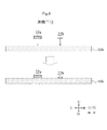
- FIG. 4 is a cross-sectional view of the multilayer board 10 at the time of manufacture.
- FIG. 5 is a cross-sectional view of the multilayer board 10 at the time of manufacture.
- FIG. 6 is a cross-sectional view of the multilayer board 10 at the time of manufacture.
- FIG. 7 is a cross-sectional view of the multilayer board 10 at the time of manufacture.
- FIG. 8 is a cross-sectional view of the multilayer board 10 at the time of manufacture.
- FIG. 11 is a cross-sectional view of the multilayer board 10a.
- FIG. 11 is a cross-sectional view of the multilayer board 10b.
- FIG. 11 is a cross-sectional view of the multilayer substrate 10c.
- FIG. 12 is a cross-sectional view of the multilayer substrate 10c at the time of manufacture.
- FIG. 13 is a cross-sectional view of the multilayer substrate 10c at the time of manufacture.
- FIG. 14 is a cross-sectional view of the multilayer board 10d.
- FIG. 15 is a cross-sectional view of the multilayer substrate 10e.
- FIG. 1 is an exploded perspective view of the multilayer board 10.
- reference numerals are given only to the representative interlayer connection conductors v1 and v2 among the plurality of interlayer connection conductors v1 and v2.
- FIG. 2 is a cross-sectional view of the multilayer board 10 in AA of FIG.
- the direction is defined as follows.
- the stacking direction of the laminated body 12 of the multilayer board 10 is defined as the vertical direction.
- the direction in which the first conductor layer 22a of the multilayer board 10 extends is defined as the front-rear direction.
- the line width direction of the first conductor layer 22a is defined as the left-right direction.
- the vertical direction, the front-back direction, and the left-right direction are orthogonal to each other.
- X is a component or member of the multilayer board 10. Unless otherwise specified, each part of X is defined as follows in the present specification.
- the front part of X means the front half of X.
- the rear part of X means the rear half of X.
- the left part of X means the left half of X.
- the right part of X means the right half of X.
- the upper part of X means the upper half of X.
- the lower part of X means the lower half of X.
- the front end of X means the front end of X.
- the rear end of X means the rear end of X.
- the left end of X means the left end of X.
- the right end of X means the right end of X.
- the upper end of X means the upper end of X.
- the lower end of X means the lower end of X.
- the front end portion of X means the front end portion of X and its vicinity.
- the rear end portion of X means the rear end portion of X and its vicinity.
- the left end portion of X means the left end portion of X and its vicinity.
- the right end portion of X means the right end portion of X and its vicinity.
- the upper end portion of X means the upper end portion of X and its vicinity.
- the lower end portion of X means the lower end portion of X and its vicinity.
- the multilayer board 10 transmits a signal.
- the multilayer board 10 is used in an electronic device such as a smartphone to electrically connect two circuits.
- the multilayer board 10 includes a laminated body 12, protective layers 20a and 20b, a first conductor layer 22a, a second conductor layer 22b, an upper conductor layer 24, a lower conductor layer 26, and signal terminals 28a to 28d. It includes a plurality of interlayer connecting conductors v1, a plurality of interlayer connecting conductors v2, and a plurality of interlayer connecting conductors v3 to v6.
- the laminated body 12 has a plate shape. Therefore, the laminated body 12 has an upper main surface and a lower main surface. The upper and lower main surfaces of the laminate 12 have normals extending in the vertical direction. The upper main surface and the lower main surface of the laminated body 12 have a rectangular shape having long sides extending in the front-rear direction. Therefore, the length of the laminated body 12 in the front-rear direction is longer than the length of the laminated body 12 in the left-right direction.
- the laminated body 12 includes the insulator layers 16a to 16c.
- the laminated body 12 has a structure in which the insulator layers 16a to 16c are laminated in the vertical direction.
- the insulator layers 16a to 16c are arranged in this order from top to bottom.
- the insulator layers 16a to 16c have the same rectangular shape as the laminated body 12 when viewed in the vertical direction.
- the insulator layers 16a to 16c are flexible dielectric sheets.
- the material of the insulator layers 16a to 16c contains a thermoplastic resin.
- the thermoplastic resin is, for example, a liquid crystal polymer, PTFE (polytetrafluoroethylene) or the like. Further, the material of the insulator layers 16a to 16c may be polyimide.
- the laminated body 12 is a main body made of an insulating material.
- the first conductor layer 22a is provided on the laminated body 12 (main body).
- the first conductor layer 22a is provided on the insulator layer 16a among the plurality of insulator layers.
- the first conductor layer 22a is provided on the upper main surface or the lower main surface of the insulator layer 16b. In the present embodiment, the first conductor layer 22a is provided on the upper main surface of the insulator layer 16b.
- the first conductor layer 22a has a linear shape.
- the first conductor layer 22a extends in the front-rear direction.
- the first signal is transmitted to the first conductor layer 22a.
- the first signal is, for example, a signal having a frequency of 0 MHz to several tens of MHz.
- the first signal is, for example, a DC signal that functions as a power source.
- the first signal is, for example, a high frequency signal having a frequency of 13.56 MHz.
- the second conductor layer 22b is provided on the laminated body 12 (main body).
- the second conductor layer 22b is provided on the insulator layer 16b among the plurality of insulator layers. Therefore, the second conductor layer 22b is provided on the same main surface of the same insulator layer 16b as the insulator layer 16b on which the first conductor layer 22a is provided. Therefore, the vertical position of the second conductor layer 22b is the same as the vertical position of the first conductor layer 22a.
- the second conductor layer 22b is provided on the upper main surface of the insulator layer 16b.
- the second conductor layer 22b overlaps with the first conductor layer 22a when viewed in the orthogonal direction (left-right direction) orthogonal to the transmission direction (front-back direction) in which the first signal is transmitted.
- the second conductor layer 22b has a linear shape.
- the second conductor layer 22b extends in the front-rear direction.
- the second conductor layer 22b is provided to the right of the first conductor layer 22a.
- a second signal having a frequency higher than that of the first signal is transmitted to the second conductor layer 22b.
- the second signal is, for example, a high frequency signal having a frequency of 100 MHz or more.
- the upper conductor layer 24 is provided on the laminated body 12 (main body).
- the upper conductor layer 24 is provided above the first conductor layer 22a and the second conductor layer 22b so as to overlap the second conductor layer 22b when viewed in the vertical direction.
- the upper conductor layer 24 is provided on the laminated body 12.
- the upper conductor layer 24 is provided above the first conductor layer 22a and the second conductor layer 22b so as to overlap the first conductor layer 22a and the second conductor layer 22b when viewed in the vertical direction.
- the upper conductor layer 24 is provided on the upper main surface of the insulator layer 16a.
- the upper conductor layer 24 covers substantially the entire surface of the upper main surface of the insulator layer 16a.
- the upper conductor layer 24 is connected to the ground potential. Therefore, the upper conductor layer 24 is a ground conductor layer.
- the lower conductor layer 26 is provided on the laminated body 12 (main body).
- the lower conductor layer 26 is provided below the first conductor layer 22a and the second conductor layer 22b so as to overlap the second conductor layer 22b when viewed in the vertical direction.
- the lower conductor layer 26 is provided on the laminated body 12.
- the lower conductor layer 26 is provided below the first conductor layer 22a and the second conductor layer 22b so as to overlap the first conductor layer 22a and the second conductor layer 22b when viewed in the vertical direction.
- the lower conductor layer 26 is provided on the lower main surface of the insulator layer 16c.
- the lower conductor layer 26 covers substantially the entire lower main surface of the insulator layer 16c.
- the lower conductor layer 26 is connected to the ground potential. Therefore, the lower conductor layer 26 is a ground conductor layer. As a result, the first conductor layer 22a, the second conductor layer 22b, the upper conductor layer 24, and the lower conductor layer 26 have a stripline structure.
- the vertical thickness Tb of the second conductor layer 22b is smaller than the vertical thickness Ta of the first conductor layer 22a.
- the thickness Ta is, for example, 17 ⁇ m or more and 35 ⁇ m or less.
- the thickness Tb is, for example, 6 ⁇ m or more and 12 ⁇ m or less.
- the vertical thickness Tb of the second conductor layer 22b is substantially equal to the vertical thickness Tc of the upper conductor layer 24 and the vertical thickness Td of the lower conductor layer 26. That is, the vertical thickness Ta of the first conductor layer 22a is larger than the vertical thickness Tc of the upper conductor layer 24 and the vertical thickness Td of the lower conductor layer 26.
- the distance Da between the first conductor layer 22a and the upper conductor layer 24 in the vertical direction is different from that of the second conductor layer 22b and the upper conductor layer 24. Is larger than the distance Db in the vertical direction of.
- the plurality of interlayer connection conductors v1 and v2 electrically connect the upper conductor layer 24 and the lower conductor layer 26. More specifically, the plurality of interlayer connection conductors v1 and v2 penetrate the insulator layers 16a to 16c in the vertical direction. The upper ends of the plurality of interlayer connection conductors v1 and v2 are connected to the upper conductor layer 24. The lower ends of the plurality of interlayer connection conductors v1 and v2 are connected to the lower conductor layer 26.
- the plurality of interlayer connection conductors v1 are provided on the left side of the first conductor layer 22a.
- the plurality of interlayer connecting conductors v1 are arranged in a row at equal intervals in the front-rear direction.
- the plurality of interlayer connecting conductors v2 are provided on the right side of the second conductor layer 22b.
- the plurality of interlayer connecting conductors v2 are arranged in a row at equal intervals in the
- the signal terminals 28a and 28c are provided at the front end of the upper main surface of the insulator layer 16a.
- the signal terminals 28a and 28c have a rectangular shape when viewed in the vertical direction.
- the signal terminal 28a overlaps with the front end portion of the first conductor layer 22a when viewed in the vertical direction.
- the signal terminal 28c overlaps the front end portion of the second conductor layer 22b when viewed in the vertical direction.
- the upper conductor layer 24 is not provided around the signal terminals 28a and 28c so that the signal terminals 28a and 28c are insulated from the upper conductor layer 24.
- the interlayer connection conductor v3 electrically connects the signal terminal 28a and the first conductor layer 22a. Specifically, the interlayer connecting conductor v3 penetrates the insulator layer 16a in the vertical direction. The upper end of the interlayer connection conductor v3 is connected to the signal terminal 28a. The lower end of the interlayer connection conductor v3 is connected to the front end portion of the first conductor layer 22a. As a result, the signal terminal 28a is electrically connected to the first conductor layer 22a. The first signal is input / output to the first conductor layer 22a via the signal terminal 28a.
- the interlayer connection conductor v5 electrically connects the signal terminal 28c and the second conductor layer 22b. Specifically, the interlayer connecting conductor v5 penetrates the insulator layer 16a in the vertical direction. The upper end of the interlayer connection conductor v5 is connected to the signal terminal 28c. The lower end of the interlayer connection conductor v5 is connected to the front end portion of the second conductor layer 22b. As a result, the signal terminal 28c is electrically connected to the second conductor layer 22b. The second signal is input / output to the second conductor layer 22b via the signal terminal 28b.
- the signal terminals 28b, 28d and the interlayer connecting conductors v4 and v6 have a structure symmetrical with those of the signal terminals 28a and 28b and the interlayer connecting conductors v3 and v5. Therefore, the description of the signal terminals 28b and 28d and the interlayer connection conductors v4 and v6 will be omitted.
- the first conductor layer 22a, the second conductor layer 22b, the upper conductor layer 24, the lower conductor layer 26, and the signal terminals 28a to 28d as described above are, for example, on the upper main surface or the lower main surface of the insulator layers 16a to 16c. It is formed by etching the provided conductor foil.
- the conductor foil is, for example, a copper foil.
- the interlayer connection conductors v1 to v6 are, for example, through-hole conductors.
- the through-hole conductor is produced by forming through holes in the insulator layers 16a to 16c and plating the through holes.
- the interlayer connection conductors v1 to v6 may be via hole conductors.
- the via hole conductor is produced by forming through holes in the insulator layers 16a to 16c, filling the through holes with the conductive paste, and then sintering the conductive paste.
- the protective layers 20a and 20b are flexible insulator layers. However, the protective layers 20a and 20b are not a part of the laminated body 12. The protective layers 20a and 20b have the same rectangular shape as the laminated body 12 when viewed in the vertical direction.
- the protective layer 20a covers substantially the entire upper main surface of the insulator layer 16a. As a result, the protective layer 20a protects the upper conductor layer 24. However, the protective layer 20a is provided with openings h1 to h8. The opening h1 overlaps with the signal terminal 28a when viewed in the vertical direction. As a result, the signal terminal 28a is exposed to the outside from the multilayer board 10 through the opening h1. The opening h2 overlaps with the signal terminal 28c when viewed in the vertical direction. As a result, the signal terminal 28c is exposed to the outside from the multilayer board 10 through the opening h2. The opening h3 is provided to the left of the opening h1. The opening h4 is provided to the right of the opening h2.
- the upper conductor layer 24 is exposed to the outside from the multilayer substrate 10 through the openings h3 and h4.
- the structure of the openings h5 to h8 is symmetrical with the structure of the openings h1 to h4, respectively. Therefore, the description of the openings h5 to h8 will be omitted.
- the protective layer 20b covers substantially the entire lower main surface of the insulator layer 16c. As a result, the protective layer 20b protects the lower conductor layer 26.
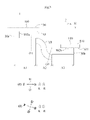
- FIG. 3 is a left side view of the electronic device 1 provided with the multilayer board 10.
- the electronic device 1 is, for example, a mobile wireless communication terminal.
- the electronic device 1 is, for example, a smartphone.
- the multilayer board 10 is bent as shown in FIG. "The multilayer board 10 is bent" means that the multilayer board 10 is deformed and bent by an external force applied to the multilayer board 10.
- the section in which the multilayer board 10 is bent is referred to as a bending section A2.
- the sections in which the multilayer board 10 cannot be bent are referred to as non-bending sections A1 and A3.
- the x-axis, y-axis, and z-axis in the electronic device 1 are defined as follows.
- the x-axis is the anteroposterior direction in the non-bending section A1.
- the y-axis is the left-right direction in the non-bending section A1.
- the z-axis is the vertical direction in the non-bending section A1.
- the non-bending section A1, the bending section A2, and the non-bending section A3 are arranged in this order in the positive direction of the x-axis.
- the bending section A2 is bent in the z-axis direction. Therefore, the vertical direction and the front-back direction differ depending on the position of the multilayer board 10 as shown in FIG.
- the non-bending section A1 and the non-bending section A3 for example, the position of (1)
- the vertical direction and the front-rear direction correspond to the z-axis direction and the x-axis direction, respectively.
- the bending section A2 for example, the position of (2) in which the laminated body 12 is bent, the vertical direction and the front-rear direction do not coincide with the z-axis direction and the x-axis direction, respectively.
- the electronic device 1 includes a multilayer board 10, connectors 30a, 30b, 102a, 102b, and circuit boards 100, 110.
- the circuit boards 100 and 110 have a plate shape.
- the circuit board 100 has main surfaces S5 and S6.
- the main surface S5 is located on the negative side of the z-axis with respect to the main surface S6.
- the circuit board 110 has main surfaces S11 and S12.
- the main surface S11 is located on the negative side of the z-axis with respect to the main surface S12.
- the circuit boards 100 and 110 include a wiring conductor layer, a ground conductor layer, electrodes and the like (not shown).
- Each of the connectors 30a and 30b is mounted on the main surface (upper main surface) on the positive direction side of the z-axis of the non-bending section A1 and the non-bending section A3. More specifically, the connector 30a is mounted on the signal terminals 28a, 28c and the upper conductor layer 24 exposed from the openings h1 to h4. The connector 30b is mounted on the signal terminals 28b and 28d exposed from the openings h5 to h8 and the upper conductor layer 24.
- Each of the connectors 102a and 102b is mounted on the main surface S5 of the circuit board 100 and the main surface S11 of the circuit board 110.
- Each of the connectors 102a and 102b is connected to the connectors 30a and 30b.
- the multilayer board 10 electrically connects the circuit board 100 and the circuit board 110.
- an insulator layer 16b (third insulator layer) in which the first conductor layer 22a and the second conductor layer 22b having different thicknesses in the vertical direction are provided on either the upper main surface or the lower main surface is prepared (3rd insulator layer). Preparation process).
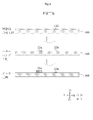
- an insulator layer 16b (third insulator layer) in which the first conductor layer 22a and the second conductor layer 22b having different thicknesses in the vertical direction are provided on the upper main surface is prepared. More specifically, as shown in FIG. 4, a conductor foil is formed on the insulator layer 16b (conductor foil preparation step).
- the copper foil 122 is attached to the upper main surface of the insulator layer 16b.
- a mask (not shown) is formed on the portion where the first conductor layer 22a and the second conductor layer 22b are formed, and the copper foil 122 is etched (patterning step).
- the vertical thickness Ta of the first conductor layer 22a and the vertical thickness Tb of the second conductor layer 22b are equal.
- the vertical thickness Ta of the first conductor layer 22a is increased in the vertical direction of the second conductor layer 22b.
- the thickness of Tb is made larger than the thickness Tb (plating process). More specifically, a mask (not shown) is formed on the second conductor layer 22b. Then, only the first conductor layer 22a is plated.
- the upper conductor layer 24 and the lower conductor layer are formed by forming a conductor foil on the upper main surface of the insulator layer 16a and the lower main surface of the insulator layer 16c and etching the conductor foil. Form 26.
- the insulator layers 16a to 16c including the insulator layer 16b (third insulator layer) are laminated in the vertical direction.
- the insulator layers 16a to 16c are subjected to heat treatment and pressure treatment (crimping step).
- the insulator layers 16a to 16c made of the thermoplastic resin are softened and fluidized, and the insulator layers 16a to 16c are bonded to each other.
- the laminated body 12 is obtained.
- the interlayer connection conductors v1 to v6 are formed.
- the interlayer connection conductors v1 to v6 are manufactured by forming through holes in the insulator layers 16a to 16c and plating the through holes.
- the protective layers 20a and 20b are formed by printing on the upper main surface of the insulator layer 16a and the lower main surface of the insulator layer 16b, respectively. Through the above steps, the multilayer board 10 is completed.
- the multilayer board 10 it is possible to reduce the transmission loss generated in the first conductor layer 22a and the second conductor layer 22b in which signals having different frequencies are transmitted. More specifically, in order to reduce the transmission loss generated in the first conductor layer 22a and the second conductor layer 22b, for example, the vertical thickness Ta of the first conductor layer 22a and the vertical direction of the second conductor layer 22b. It is conceivable to increase the thickness Tb. In this case, the DC resistance values of the first conductor layer 22a and the second conductor layer 22b can be reduced.
- a second signal having a frequency higher than that of the first signal is transmitted to the second conductor layer 22b.
- a predetermined characteristic impedance for example, 50 ⁇ . Therefore, the line width in the left-right direction of the second conductor layer 22b and the distance Da in the vertical direction between the second conductor layer 22b and the upper conductor layer 24 so that the characteristic impedance generated in the second conductor layer 22b approaches a predetermined characteristic impedance. Is designed.
- the vertical thickness Ta of the first conductor layer 22a and the vertical thickness Tb of the second conductor layer 22b are increased as described above, the distance between the second conductor layer 22b and the upper conductor layer 24 in the vertical direction is increased. Da becomes smaller than the design value.
- the capacitance value generated between the second conductor layer 22b and the upper conductor layer 24 becomes larger than the design value, and the characteristic impedance generated in the second conductor layer 22b fluctuates from a predetermined characteristic impedance. Therefore, it is difficult to reduce the transmission loss generated in the second conductor layer 22b.
- the transmission loss of the first conductor layer 22a is reduced.
- the condition for reducing the transmission loss of the second conductor layer 22b are different. Therefore, by increasing the vertical thickness Ta of the first conductor layer 22a and the vertical thickness Tb of the second conductor layer 22b, the transmission loss generated in the first conductor layer 22a and the second conductor layer 22b can be reduced. Is difficult.
- the vertical thickness Tb of the second conductor layer 22b is smaller than the vertical thickness Ta of the first conductor layer 22a.
- the capacitance value generated between the second conductor layer 22b and the upper conductor layer 24 becomes larger than the design value, and the characteristic impedance generated in the second conductor layer 22b fluctuates from a predetermined characteristic impedance. Is suppressed.
- the capacitance value generated between the second conductor layer 22b and the upper conductor layer 24 becomes large, it becomes easy to increase the line width in the left-right direction of the second conductor layer 22b.
- the length of the outer edge of the second conductor layer 22b in the cross section orthogonal to the front-rear direction tends to be long.
- the region where the second signal can flow tends to be widened in the second conductor layer 22b. Therefore, the transmission loss of the second conductor layer 22b is likely to be reduced. From the above, according to the multilayer board 10, it is possible to reduce the transmission loss generated in the first conductor layer 22a and the second conductor layer 22b in which signals having different frequencies are transmitted.
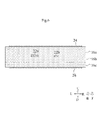
- FIG. 7 is a cross-sectional view of the multilayer board 10 at the time of manufacture.
- the method for manufacturing the multilayer board 10 according to the first modification is different from the method for manufacturing the multilayer board 10 according to the embodiment in the preparation step. More specifically, as shown in FIG. 7, a conductor foil is formed on the insulator layer 16b (third insulator layer) (conductor foil forming step). In this modification, the copper foil 122 is attached to the upper main surface of the insulator layer 16b.
- a mask (not shown) is formed on the portion where the first conductor layer 22a and the second conductor layer 22b are formed, and the copper foil 122 is etched (patterning step).
- the vertical thickness Ta of the first conductor layer 22a and the vertical thickness Tb of the second conductor layer 22b are equal.
- the vertical thickness Tb of the second conductor layer 22b is made smaller than the vertical thickness Ta of the first conductor layer 22a (). Etching process). More specifically, a mask (not shown) is formed on the first conductor layer 22a. Then, only the second conductor layer 22b is etched. Since the other steps of the method for manufacturing the multilayer board 10 according to the first modification are the same as the method for manufacturing the multilayer board 10 according to the embodiment, the description thereof will be omitted.
- the multilayer board 10 can also be obtained by the method for manufacturing the multilayer board 10 according to the first modification.
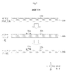
- FIG. 8 is a cross-sectional view of the multilayer board 10 at the time of manufacture.
- the method for manufacturing the multilayer board 10 according to the second modification is different from the method for manufacturing the multilayer board 10 according to the embodiment in the preparation step. More specifically, as shown in FIG. 8, in the preparation step, the first conductor layer 22a and the second conductor layer 22b having different thicknesses in the vertical direction are formed on the upper main surface of the insulator layer 16b (third insulator layer) or. Paste it on one of the lower main surfaces. That is, the first conductor layer 22a and the second conductor layer 22b having different thicknesses in the vertical direction are manufactured. Then, the first conductor layer 22a and the second conductor layer 22b are attached to the upper main surface of the insulator layer 16b.
- the multilayer board 10 can also be obtained by the method for manufacturing the multilayer board 10 according to the second modification.
- FIG. 9 is a cross-sectional view of the multilayer substrate 10a.
- the multilayer substrate 10a is different from the multilayer substrate 10 in that the vertical thickness of the left portion of the laminated body 12 is different from the vertical thickness of the right portion of the laminated body 12. This difference will be described below.
- the laminated body 12 further includes the insulator layers 16d and 16e.
- the insulator layers 16d and 16e are laminated from top to bottom in this order between the insulator layer 16b and the insulator layer 16c.
- the multilayer board 10a further includes ground conductor layers 30, 31, and 32.
- Each of the ground conductor layers 30, 31 and 32 is located on the upper main surface of the insulator layers 16d, 16e and 16c.
- Each of the ground conductor layers 30, 31, and 32 overlaps with the first conductor layer 22a when viewed in the vertical direction.
- Each of the ground conductor layers 30, 31, and 32 does not overlap with the second conductor layer 22b when viewed in the vertical direction. This is to suppress deterioration of the high frequency characteristics of the multilayer substrate 10a by reducing the capacitance formed between the second conductor layer 22b and the ground conductor layers 30, 31, 32.
- each of the ground conductor layers 30, 31, and 32 does not overlap with the second conductor layer 22b when viewed in the vertical direction. Therefore, when the laminated body 12 is crimped, the vertical thickness of the left portion of the laminated body 12 becomes larger than the vertical thickness of the right portion of the laminated body 12.
- the distance Da in the vertical direction between the first conductor layer 22a and the upper conductor layer 24 is larger than the distance Db in the vertical direction between the second conductor layer 22b and the upper conductor layer 24.
- the multilayer board 10a can reduce the transmission loss generated in the first conductor layer 22a and the second conductor layer 22b in which signals having different frequencies are transmitted for the same reason as the multilayer board 10.
- FIG. 10 is a cross-sectional view of the multilayer board 10b.
- the multilayer board 10b is different from the multilayer board 10a in that the boundaries between the insulator layers 16a to 16e cannot be visually recognized. Further, in the multilayer board 10b, the second conductor layer 22b overlaps with the first conductor layer 22a when viewed in an orthogonal direction orthogonal to the transmission direction in which the first signal is transmitted.
- the multilayer board 10b can reduce the transmission loss generated in the first conductor layer 22a and the second conductor layer 22b in which signals having different frequencies are transmitted for the same reason as the multilayer board 10a.
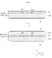
- FIG. 11 is a cross-sectional view of the multilayer substrate 10c.
- the multilayer board 10c is different from the multilayer board 10 in that the insulator layer 18 is further provided instead of the insulator layer 16c, and the lower conductor layer 26 is provided on the lower main surface of the insulator layer 16b. It's different. Hereinafter, the multilayer board 10c will be described focusing on these differences.
- the laminate 12 includes an insulator layer 16a (first insulator layer), an insulator layer 16b (third insulator layer), and an insulator layer 18 (second insulator layer).
- the insulator layer 16a (first insulator layer) and the insulator layer 18 (second insulator layer) are placed below the upper conductor layer 24 and above the first conductor layer 22a and the second conductor layer 22b, respectively. They are stacked so as to be adjacent to each other in this order from top to bottom.
- the insulator layer 16b is provided below the insulator layer 18.
- the boundary between the insulator layer 16a and the insulator layer 18 is located between the lower main surface of the upper conductor layer 24, the lower main surface of the first conductor layer 22a, and the lower main surface of the second conductor layer 22b.
- the material of the insulator layer 16b (third insulator layer) is the same as the material of the insulator layer 16a (first insulator layer). "The material of the insulator layer 16b is the same as the material of the insulator layer 16a" means that an error due to manufacturing variation is allowed.
- the material of the insulator layer 18 is different from the material of the insulator layers 16a and 16b.
- the insulator layer 18 (second insulator layer) is an adhesive layer that joins the insulator layer 16a (first insulator layer) and the insulator layer 16b (third insulator layer). Further, the dielectric constant of the insulator layer 18 (second insulator layer) is lower than the dielectric constant of the insulator layer 16a (first insulator layer). Further, the dielectric loss tangent of the insulator layer 18 (second insulator layer) is lower than the dielectric loss tangent of the insulator layer 18 (first insulator layer).
- the material of the insulator layer 18 satisfying these conditions is, for example, a fluororesin. However, the material of the insulator layer 18 may be an epoxy resin, an acrylic resin, or the like.
- the first conductor layer 22a and the second conductor layer 22b are provided on the insulator layer 16b (third insulator layer). In the present embodiment, the first conductor layer 22a and the second conductor layer 22b are provided on the upper main surface of the insulator layer 16b (third insulator layer).
- the upper conductor layer 24 is provided on the insulator layer 16a (first insulator layer). In the present embodiment, the upper conductor layer 24 is provided on the upper main surface of the insulator layer 16a (first insulator layer).
- the lower conductor layer 26 is provided on the lower main surface of the insulator layer 16b (third insulator layer). Since the other structures of the multilayer board 10c are the same as those of the multilayer board 10, the description thereof will be omitted.
- an insulator layer 16b (third insulator layer) in which the first conductor layer 22a and the second conductor layer 22b having different thicknesses in the vertical direction are provided on either the upper main surface or the lower main surface is prepared (3rd insulator layer). Preparation process).
- an insulator layer 16b (third insulator layer) in which the first conductor layer 22a and the second conductor layer 22b having different thicknesses in the vertical direction are provided on the upper main surface is prepared. More specifically, as shown in FIG. 12, a conductor foil is formed on the insulator layer 16b (conductor foil preparation step).
- copper foils 122 and 126 are attached to the upper main surface and the lower main surface of the insulator layer 16b, respectively.
- a mask (not shown) is formed on the portion where the first conductor layer 22a and the second conductor layer 22b are formed, and the copper foil 122 is etched.
- a mask (not shown) is formed on the portion where the lower conductor layer 26 is formed, and the copper foil 126 is etched.
- the vertical thickness Ta of the first conductor layer 22a and the vertical thickness Tb of the second conductor layer 22b are equal.
- the etching of the copper foil 122 and the etching of the copper foil 126 may be performed at the same time.
- the vertical thickness Ta of the first conductor layer 22a is increased in the vertical direction of the second conductor layer 22b.
- the thickness of Tb is made larger than the thickness Tb (plating process). More specifically, a mask (not shown) is formed on the second conductor layer 22b and the lower conductor layer 26. Then, only the first conductor layer 22a is plated.
- the conductor foil is formed on the upper main surface of the insulator layer 16a, and the conductor foil is etched to form the upper conductor layer 24.
- the insulator layer 16a (first insulator layer), the insulator layer 18 (second insulator layer) which is an adhesive layer without a conductor layer, and the insulator layer 16b (third insulator layer). ) are arranged and stacked in this order from top to bottom.
- the insulator layer 18a which is an adhesive layer, is formed on the upper main surface of the insulator layer 16b (adhesive layer forming step).
- a liquid resin is applied to the upper main surface of the insulator layer 16b.
- the insulator layer 16a is arranged on the insulator layer 18a (arrangement step).
- the insulator layer 16a first insulator layer
- the insulator layer 16b third insulator layer
- the insulator layer 18 adheresive layer
- the insulator layer 18 functions as an adhesive layer
- the insulator layer 16a and the insulator layer 16b are joined to each other.
- the adhesive layer forming step, the arranging step, and the crimping step are repeated.
- the interlayer connection conductors v1 to v6 are formed.
- the interlayer connection conductors v1 to v6 are manufactured by forming through holes in the insulator layers 16a to 16c and plating the through holes.
- each of the protective layers 20a and 20b is formed on the upper main surface of the insulator layer 16a and the lower main surface of the insulator layer 16b by printing. Through the above steps, the multilayer substrate 10c is completed.
- the insulator layers 16a and 18 are arranged in this order from top to bottom so as to be adjacent to each other below the upper conductor layer 24 and above the first conductor layer 22a and the second conductor layer 22b. It is laminated like this.
- the dielectric constant of the insulator layer 18 is lower than the dielectric constant of the insulator layer 16a.
- the dielectric loss tangent of the insulator layer 18 is lower than the dielectric loss tangent of the insulator layer 16a. As a result, the dielectric constant and the dielectric loss tangent in the vicinity of the second conductor layer 22b are lowered.
- the second signal which is a high frequency signal
- the second conductor layer 22b when the second signal, which is a high frequency signal, is transmitted to the second conductor layer 22b, it is possible to suppress the occurrence of dielectric loss in the second conductor layer 22b.
- the multilayer board 10c it is possible to more effectively reduce the transmission loss of the second conductor layer 22b.
- the materials of the insulator layers 16a and 16b may be a thermoplastic resin or may not be a thermoplastic resin.
- FIG. 14 is a cross-sectional view of the multilayer board 10d.
- the multilayer board 10d is different from the multilayer board 10 in that the ground conductor layers 27a and 27b are further provided.
- the ground conductor layers 27a and 27b are connected to the ground potential.
- the ground conductor layers 27a and 27b are provided on the upper main surface of the insulator layer 16b.
- the ground conductor layer 27a is provided between the first conductor layer 22a and the second conductor layer 22b. Further, the ground conductor layer 27b is provided on the right side of the second conductor layer 22b. Since the other structures of the multilayer board 10d are the same as those of the multilayer board 10, the description thereof will be omitted.
- the multilayer board 10d it is possible to reduce the transmission loss generated in the first conductor layer 22a and the second conductor layer 22b in which signals having different frequencies are transmitted for the same reason as the multilayer board 10.
- the ground conductor layer 27a is provided between the first conductor layer 22a and the second conductor layer 22b. This increases the isolation between the first conductor layer 22a and the second conductor layer 22b.
- the ground conductor layers 27a and 27b may be electrically connected to at least one of the upper conductor layer 24 and the lower conductor layer 26 by an interlayer connecting conductor. As a result, the potentials of the ground conductor layers 27a and 27b are stabilized at the ground potential.
- FIG. 15 is a cross-sectional view of the multilayer substrate 10e.
- the multilayer board 10e is different from the multilayer board 10c in that the ground conductor layers 27a and 27b are further provided.
- the ground conductor layers 27a and 27b are connected to the ground potential.
- the ground conductor layers 27a and 27b are provided on the upper main surface of the insulator layer 16b.
- the ground conductor layer 27a is provided between the first conductor layer 22a and the second conductor layer 22b. Further, the ground conductor layer 27b is provided on the right side of the second conductor layer 22b. Since the other structures of the multilayer board 10e are the same as those of the multilayer board 10c, the description thereof will be omitted.
- the multilayer board 10e it is possible to reduce the transmission loss generated in the first conductor layer 22a and the second conductor layer 22b in which signals having different frequencies are transmitted for the same reason as the multilayer board 10c.
- the ground conductor layer 27a is provided between the first conductor layer 22a and the second conductor layer 22b. This increases the isolation between the first conductor layer 22a and the second conductor layer 22b.
- the multilayer board according to the present invention is not limited to the multilayer boards 10, 10a to 10e, and can be changed within the scope of the gist thereof.
- the configurations of the multilayer boards 10, 10a to 10e may be arbitrarily combined.
- the insulator layers 16a to 16c may have a structure in which a glass cloth is impregnated with an epoxy resin. In this case, the multilayer boards 10, 10a to 10e do not have flexibility.
- the lower conductor layer 26 is not an essential configuration in the multilayer boards 10, 10a to 10e.
- the first conductor layer 22a and the upper conductor layer 24 have a microstrip line structure.
- the second conductor layer 22b and the upper conductor layer 24 have a microstrip line structure.
- the interlayer connection conductors v1 and v2 are not essential configurations.
- the multilayer boards 10, 10a to 10e are transmission lines. However, the multilayer boards 10, 10a to 10e may be circuit boards. Therefore, the multilayer boards 10, 10a to 10e may further include other circuits in addition to the stripline line.
- the signal terminals 28a to 28d may be provided on the lower main surface of the laminated body 12.
- the multilayer boards 10, 10a to 10e have a linear shape when viewed in the vertical direction. However, the multilayer boards 10, 10a to 10e may be bent. Here, “the multilayer boards 10, 10a to 10e are bent” means that the multilayer boards 10, 10a to 10e have a bent shape without applying an external force.
- the first conductor layer 22a and the second conductor layer 22b do not have to extend in parallel.
- the insulator layer 18 may be formed by attaching a resin sheet to the upper main surface of the insulator layer 16b.
- the dielectric constant of the insulator layer 18 may be equal to or higher than the dielectric constant of the insulator layer 16a, and the dielectric loss tangent of the insulator layer 18 may be lower than the dielectric loss tangent of the insulator layer 16a.
- the dielectric constant of the insulator layer 18 may be lower than the dielectric constant of the insulator layer 16a, and the dielectric loss tangent of the insulator layer 18 may be greater than or equal to the dielectric loss tangent of the insulator layer 16a.
- the dielectric constant of the insulator layer 18 may be equal to or higher than the dielectric constant of the insulator layer 16a, and the dielectric loss tangent of the insulator layer 18 may be equal to or higher than the dielectric loss tangent of the insulator layer 16a.
- the patterning step may be performed after the plating step.
- a patterning step may be performed after the etching step.
- the upper conductor layer 24 and the lower conductor layer 26 may be connected to a potential other than the ground potential.
- the upper conductor layer 24 does not have to overlap with the first conductor layer 22a when viewed in the vertical direction.
- the lower conductor layer 26 does not have to overlap with the first conductor layer 22a when viewed in the vertical direction.
- the second conductor layer 22b may overlap with the first conductor layer 22a when viewed in an orthogonal direction orthogonal to the transmission direction in which the first signal is transmitted.
Landscapes
- Engineering & Computer Science (AREA)
- Microelectronics & Electronic Packaging (AREA)
- Physics & Mathematics (AREA)
- Electromagnetism (AREA)
- Manufacturing & Machinery (AREA)
- Production Of Multi-Layered Print Wiring Board (AREA)
Abstract
Description
複数の絶縁体層が上下方向に積層された構造を有している積層体と、
前記絶縁体層の上主面又は下主面に設けられており、かつ、第1信号が伝送される第1導体層と、
前記第1導体層が設けられている前記絶縁体層の上主面又は下主面と同じ前記絶縁体層の同一主面に設けられており、かつ、前記第1信号より高い周波数を有する第2信号が伝送される第2導体層と、
前記積層体に設けられており、かつ、上下方向に見て、前記第2導体層と重なるように、前記第1導体層及び前記第2導体層より上に設けられている上導体層と、
を備えており、
前記第2導体層の上下方向の厚みは、前記第1導体層の上下方向の厚みより小さい。
上下方向の厚みの異なる第1導体層及び第2導体層が上主面又は下主面のいずれか一方に設けられた第3絶縁体層を準備する準備工程と、
前記第3絶縁体層を含む複数の絶縁体層を上下方向に積層した後に、前記複数の絶縁体層に加熱処理及び加圧処理を施す圧着工程と、
を備えており、
前記複数の絶縁体層の材料は、熱可塑性樹脂を含んでいる。
複数の絶縁体層が上下方向に積層された構造を有している積層体と、
前記複数の絶縁体層の内の絶縁体層に設けられており、かつ、第1信号が伝送される第1導体層と、
前記複数の絶縁体層の内の絶縁体層に設けられており、前記第1信号より高い周波数を有する第2信号が伝送される第2導体層と、
前記積層体に設けられており、かつ、上下方向に見て、前記第2導体層と重なるように、前記第1導体層及び前記第2導体層より上に設けられている上導体層と、
を備えており、
前記第1信号が伝送される伝送方向に直交する直交方向に見て、前記第2導体層は、前記第1導体層に重なっており、
前記第2導体層の上下方向の厚みは、前記第1導体層の上下方向の厚みより小さい。
上下方向の厚みの異なる第1導体層及び第2導体層が上主面又は下主面のいずれか一方に設けられた第3絶縁体層を準備する準備工程と、
第1絶縁体層、導体層が設けられていない接着層である第2絶縁体層、及び、前記第3絶縁体層を上から下へとこの順に並べて積層した後に、前記第1絶縁体層、前記第2絶縁体層及び前記第3絶縁体層に加熱処理及び加圧処理を施す圧着工程と、
を備えている。
[多層基板10の構造]
以下に、本発明の実施形態に係る多層基板10の構造について図面を参照しながら説明する。図1は、多層基板10の分解斜視図である。なお、図1では、複数の層間接続導体v1,v2の内の代表的な層間接続導体v1,v2にのみ参照符号を付した。図2は、図1のA-Aにおける多層基板10の断面図である。
次に、多層基板10を備える電子機器1の構造について図面を参照しながら説明する。図3は、多層基板10を備える電子機器1の左面図である。電子機器1は、例えば、携帯無線通信端末である。電子機器1は、例えば、スマートフォンである。
以下に、多層基板10の製造方法について図面を参照しながら説明する。図4ないし図6は、多層基板10の製造時における断面図である。
多層基板10によれば、異なる周波数の信号が伝送される第1導体層22a及び第2導体層22bに生じる伝送損失を低減できる。より詳細には、第1導体層22a及び第2導体層22bに生じる伝送損失を低減するためには、例えば、第1導体層22aの上下方向の厚みTa及び第2導体層22bの上下方向の厚みTbを大きくすることが考えられる。この場合、第1導体層22a及び第2導体層22bの直流抵抗値を低減することができる。
以下に第1変形例に係る多層基板10の製造方法について図面を参照しながら説明する。図7は、多層基板10の製造時における断面図である。
以下に第2変形例に係る多層基板10の製造方法について図面を参照しながら説明する。図8は、多層基板10の製造時における断面図である。
以下に第3変形例に係る多層基板10aについて図面を参照しながら説明する。図9は、多層基板10aの断面図である。
以下に第4変形例に係る多層基板10bについて図面を参照しながら説明する。図10は、多層基板10bの断面図である。
[多層基板10cの構造]
以下に第5変形例に係る多層基板10cについて図面を参照しながら説明する。図11は、多層基板10cの断面図である。
以下に、多層基板10cの製造方法について図面を参照しながら説明する。図12及び図13は、多層基板10cの製造時における断面図である。
多層基板10cによれば、多層基板10と同じ理由により、異なる周波数の信号が伝送される第1導体層22a及び第2導体層22bに生じる伝送損失を低減できる。
以下に第6変形例に係る多層基板10dについて図面を参照しながら説明する。図14は、多層基板10dの断面図である。
以下に第7変形例に係る多層基板10eについて図面を参照しながら説明する。図15は、多層基板10eの断面図である。
本発明に係る多層基板は、多層基板10,10a~10eに限らず、その要旨の範囲内において変更可能である。なお、多層基板10,10a~10eの構成を任意に組み合わせてもよい。
10,10a~10e:多層基板
12:積層体
16a~16e,18:絶縁体層
20a,20b:保護層
22a:第1導体層
22b:第2導体層
24:上導体層
26:下導体層
27a,27b,30~32:グランド導体層
28a~28d:信号端子
122,126:銅箔
Claims (18)
- 複数の絶縁体層が上下方向に積層された構造を有している積層体と、
前記絶縁体層の上主面又は下主面に設けられており、かつ、第1信号が伝送される第1導体層と、
前記第1導体層が設けられている前記絶縁体層の上主面又は下主面と同じ前記絶縁体層の同一主面に設けられており、かつ、前記第1信号より高い周波数を有する第2信号が伝送される第2導体層と、
前記積層体に設けられており、かつ、上下方向に見て、前記第2導体層と重なるように、前記第1導体層及び前記第2導体層より上に設けられている上導体層と、
を備えており、
前記第2導体層の上下方向の厚みは、前記第1導体層の上下方向の厚みより小さい、
多層基板。 - 前記複数の絶縁体層は、第1絶縁体層及び第2絶縁体層を含んでおり、
前記第1絶縁体層及び前記第2絶縁体層は、前記上導体層より下、かつ、前記第1導体層及び前記第2導体層より上において、互いに隣接するように上から下へとこの順に並ぶように積層されており、
前記第2絶縁体層の誘電率は、前記第1絶縁体層の誘電率より低い、
請求項1に記載の多層基板。 - 前記複数の絶縁体層は、第1絶縁体層及び第2絶縁体層を含んでおり、
前記第1絶縁体層及び前記第2絶縁体層は、前記上導体層より下、かつ、前記第1導体層及び前記第2導体層より上において、互いに隣接するように上から下へとこの順に並ぶように積層されており、
前記第2絶縁体層の誘電正接は、前記第1絶縁体層の誘電正接より低い、
請求項1又は請求項2に記載の多層基板。 - 前記複数の絶縁体層は、第3絶縁体層を更に含んでおり、
前記第1導体層及び前記第2導体層は、前記第3絶縁体層に設けられており、
前記第3絶縁体層の材料は、前記第1絶縁体層の材料と同じであり、
前記第2絶縁体層は、前記第1絶縁体層と前記第3絶縁体層とを接合する接着層である、
請求項2又は請求項3のいずれかに記載の多層基板。 - 前記上導体層は、前記第1絶縁体層に設けられている、
請求項4に記載の多層基板。 - 前記多層基板は、
前記積層体に設けられており、かつ、上下方向に見て、前記第2導体層と重なるように、前記第1導体層及び前記第2導体層より下に設けられている下導体層を、
更に備えている、
請求項1ないし請求項5のいずれかに記載の多層基板。 - 前記多層基板は、
前記第1導体層と前記第2導体層との間に設けられているグランド導体層を、
更に備えている、
請求項1ないし請求項6のいずれかに記載の多層基板。 - 前記第1信号は、電源として機能する直流信号である、
請求項1ないし請求項7のいずれかに記載の多層基板。 - 前記第2導体層と前記上導体層との上下方向における距離は、前記第1導体層と前記上導体層との上下方向における距離より大きい、
請求項1ないし請求項8のいずれかに記載の多層基板。 - 前記上導体層は、上下方向に見て、前記第1導体層と重なっている、
請求項1ないし請求項9のいずれかに記載の多層基板。 - 前記上導体層は、グランド導体層である、
請求項1ないし請求項10のいずれかに記載の多層基板。 - 絶縁材料を材料とする本体と、
前記本体に設けられており、かつ、第1信号が伝送される第1導体層と、
前記本体に設けられており、前記第1信号より高い周波数を有する第2信号が伝送される第2導体層と、
前記本体に設けられており、かつ、上下方向に見て、前記第2導体層と重なるように、前記第1導体層及び前記第2導体層より上に設けられている上導体層と、
を備えており、
前記第1信号が伝送される伝送方向に直交する直交方向に見て、前記第2導体層は、前記第1導体層に重なっており、
前記第2導体層の上下方向の厚みは、前記第1導体層の上下方向の厚みより小さい、
多層基板。 - 上下方向の厚みの異なる第1導体層及び第2導体層が上主面又は下主面のいずれか一方に設けられた第3絶縁体層を準備する準備工程と、
前記第3絶縁体層を含む複数の絶縁体層を上下方向に積層した後に、前記複数の絶縁体層に加熱処理及び加圧処理を施す圧着工程と、
を備えており、
前記複数の絶縁体層の材料は、熱可塑性樹脂を含んでいる、
多層基板の製造方法。 - 上下方向の厚みの異なる第1導体層及び第2導体層が上主面又は下主面のいずれか一方に設けられた第3絶縁体層を準備する準備工程と、
第1絶縁体層、導体層が設けられていない接着層である第2絶縁体層、及び、前記第3絶縁体層を上から下へとこの順に並べて積層した後に、前記第1絶縁体層、前記第2絶縁体層及び前記第3絶縁体層に加熱処理及び加圧処理を施す圧着工程と、
を備えている、
多層基板の製造方法。 - 前記準備工程は、
導体箔を前記第3絶縁体層に形成する導体箔形成工程と、
前記導体箔の一部にメッキ処理を施すことにより、前記第1導体層の上下方向の厚みを前記第2導体層の上下方向の厚みより大きくするメッキ工程と、
を含んでいる、
請求項13又は請求項14に記載の多層基板の製造方法。 - 前記準備工程は、
導体箔を前記第3絶縁体層に形成する導体箔形成工程と、
前記導体箔の一部にエッチング処理を施すことにより、前記第2導体層の上下方向の厚みを前記第1導体層の上下方向の厚みより小さくするエッチング工程と、
を含んでいる、
請求項13又は請求項14に記載の多層基板の製造方法。 - 前記準備工程では、上下方向の厚みの異なる前記第1導体層及び前記第2導体層を前記第3絶縁体層の上主面又は下主面のいずれかに貼り付ける、
請求項13又は請求項14のいずれかに記載の多層基板の製造方法。 - 前記多層基板は、
複数の絶縁体層が上下方向に積層された構造を有する積層体と、
前記第3絶縁体層の上主面又は下主面に設けられており、かつ、第1信号が伝送される第1導体層と、
前記第1導体層が設けられている前記第3絶縁体層の上主面又は下主面と同じ前記第3絶縁体層の同一主面に設けられており、かつ、前記第1信号より高い周波数を有する第2信号が伝送される第2導体層と、
前記積層体に設けられており、かつ、上下方向に見て、前記第2導体層と重なるように、前記第1導体層及び前記第2導体層より上に設けられている上導体層と、
を備えており、
前記第2導体層の上下方向の厚みは、前記第1導体層の上下方向の厚みより小さい、
請求項13ないし請求項17のいずれかに記載の多層基板の製造方法。
Priority Applications (3)
| Application Number | Priority Date | Filing Date | Title |
|---|---|---|---|
| CN202190000941.9U CN219626872U (zh) | 2020-12-24 | 2021-12-15 | 多层基板 |
| JP2022572212A JP7597128B2 (ja) | 2020-12-24 | 2021-12-15 | 多層基板及び多層基板の製造方法 |
| US18/207,169 US12431603B2 (en) | 2020-12-24 | 2023-06-08 | Multilayer substrate and manufacturing method therefor |
Applications Claiming Priority (2)
| Application Number | Priority Date | Filing Date | Title |
|---|---|---|---|
| JP2020-214600 | 2020-12-24 | ||
| JP2020214600 | 2020-12-24 |
Related Child Applications (1)
| Application Number | Title | Priority Date | Filing Date |
|---|---|---|---|
| US18/207,169 Continuation US12431603B2 (en) | 2020-12-24 | 2023-06-08 | Multilayer substrate and manufacturing method therefor |
Publications (1)
| Publication Number | Publication Date |
|---|---|
| WO2022138355A1 true WO2022138355A1 (ja) | 2022-06-30 |
Family
ID=82159094
Family Applications (1)
| Application Number | Title | Priority Date | Filing Date |
|---|---|---|---|
| PCT/JP2021/046177 Ceased WO2022138355A1 (ja) | 2020-12-24 | 2021-12-15 | 多層基板及び多層基板の製造方法 |
Country Status (4)
| Country | Link |
|---|---|
| US (1) | US12431603B2 (ja) |
| JP (1) | JP7597128B2 (ja) |
| CN (1) | CN219626872U (ja) |
| WO (1) | WO2022138355A1 (ja) |
Cited By (1)
| Publication number | Priority date | Publication date | Assignee | Title |
|---|---|---|---|---|
| JPWO2024237037A1 (ja) * | 2023-05-17 | 2024-11-21 |
Citations (4)
| Publication number | Priority date | Publication date | Assignee | Title |
|---|---|---|---|---|
| JPH02109390A (ja) * | 1988-10-18 | 1990-04-23 | Furukawa Electric Co Ltd:The | 高密度フレキシブルプリント回路基板 |
| JPH09199816A (ja) * | 1996-01-16 | 1997-07-31 | Sumitomo Wiring Syst Ltd | フレキシブルプリント基板およびその製造方法 |
| JP2003133660A (ja) * | 2001-10-19 | 2003-05-09 | G Tekku:Kk | 電源用と信号用回路が複合されたフレキシブルプリント配線板 |
| JP2020164870A (ja) * | 2014-09-24 | 2020-10-08 | 東亞合成株式会社 | 接着剤組成物及びこれを用いた接着剤層付き積層体 |
Family Cites Families (2)
| Publication number | Priority date | Publication date | Assignee | Title |
|---|---|---|---|---|
| JP3318739B2 (ja) | 1998-03-27 | 2002-08-26 | 日本航空電子工業株式会社 | ディファレンシャル信号伝送線路 |
| JP2022032293A (ja) * | 2020-08-11 | 2022-02-25 | 日本メクトロン株式会社 | 配線体およびその製造方法 |
-
2021
- 2021-12-15 CN CN202190000941.9U patent/CN219626872U/zh active Active
- 2021-12-15 JP JP2022572212A patent/JP7597128B2/ja active Active
- 2021-12-15 WO PCT/JP2021/046177 patent/WO2022138355A1/ja not_active Ceased
-
2023
- 2023-06-08 US US18/207,169 patent/US12431603B2/en active Active
Patent Citations (4)
| Publication number | Priority date | Publication date | Assignee | Title |
|---|---|---|---|---|
| JPH02109390A (ja) * | 1988-10-18 | 1990-04-23 | Furukawa Electric Co Ltd:The | 高密度フレキシブルプリント回路基板 |
| JPH09199816A (ja) * | 1996-01-16 | 1997-07-31 | Sumitomo Wiring Syst Ltd | フレキシブルプリント基板およびその製造方法 |
| JP2003133660A (ja) * | 2001-10-19 | 2003-05-09 | G Tekku:Kk | 電源用と信号用回路が複合されたフレキシブルプリント配線板 |
| JP2020164870A (ja) * | 2014-09-24 | 2020-10-08 | 東亞合成株式会社 | 接着剤組成物及びこれを用いた接着剤層付き積層体 |
Cited By (3)
| Publication number | Priority date | Publication date | Assignee | Title |
|---|---|---|---|---|
| JPWO2024237037A1 (ja) * | 2023-05-17 | 2024-11-21 | ||
| WO2024237037A1 (ja) * | 2023-05-17 | 2024-11-21 | 株式会社村田製作所 | 多層基板及び電子機器 |
| JP7823794B2 (ja) | 2023-05-17 | 2026-03-04 | 株式会社村田製作所 | 多層基板及び電子機器 |
Also Published As
| Publication number | Publication date |
|---|---|
| JP7597128B2 (ja) | 2024-12-10 |
| CN219626872U (zh) | 2023-09-01 |
| US12431603B2 (en) | 2025-09-30 |
| US20230318160A1 (en) | 2023-10-05 |
| JPWO2022138355A1 (ja) | 2022-06-30 |
Similar Documents
| Publication | Publication Date | Title |
|---|---|---|
| JP7517469B2 (ja) | 伝送線路及び電子機器 | |
| JP7772040B2 (ja) | 伝送線路 | |
| CN103733736B (zh) | 高频信号传输线路及电子设备 | |
| CN205081202U (zh) | 传输线路及扁平电缆 | |
| US9059493B2 (en) | High-frequency signal line and electronic device | |
| US12389532B2 (en) | High-frequency circuit | |
| WO2014002757A1 (ja) | ケーブルの接続・固定方法 | |
| CN114144945A (zh) | 柔性电缆 | |
| US20160037622A1 (en) | Multilayer resin substrate, and method of manufacturing multilayer resin substrate | |
| JP4414365B2 (ja) | 高速伝送用基板 | |
| JP7597128B2 (ja) | 多層基板及び多層基板の製造方法 | |
| US20210273361A1 (en) | Electronic device and flat cable | |
| US12230423B2 (en) | Transmission line and electronic device | |
| JPWO2022138355A5 (ja) | ||
| CN113131165B (zh) | 电路结构 | |
| CN219981140U (zh) | 多层基板、多层基板模块以及电子设备 | |
| WO2022080067A1 (ja) | 回路基板及び回路基板の製造方法 | |
| CN220272720U (zh) | 传输线路以及电子设备 | |
| CN220306489U (zh) | 传输线路以及电子设备 | |
| JP2014175829A (ja) | 伝送線路、アンテナ装置及び伝送線路製造方法 | |
| US12438246B2 (en) | Transmission line and electronic device | |
| JP7409493B2 (ja) | 信号伝送線路及び信号伝送線路の製造方法 | |
| WO2024171659A1 (ja) | 多層基板、電子機器及び多層基板の製造方法 | |
| WO2022113739A1 (ja) | 伝送線路及び電子機器 | |
| JPWO2024171659A5 (ja) |
Legal Events
| Date | Code | Title | Description |
|---|---|---|---|
| 121 | Ep: the epo has been informed by wipo that ep was designated in this application |
Ref document number: 21910504 Country of ref document: EP Kind code of ref document: A1 |
|
| ENP | Entry into the national phase |
Ref document number: 2022572212 Country of ref document: JP Kind code of ref document: A |
|
| WWE | Wipo information: entry into national phase |
Ref document number: 202190000941.9 Country of ref document: CN |
|
| NENP | Non-entry into the national phase |
Ref country code: DE |
|
| 122 | Ep: pct application non-entry in european phase |
Ref document number: 21910504 Country of ref document: EP Kind code of ref document: A1 |