WO2022137652A1 - 車載用電子制御装置 - Google Patents
車載用電子制御装置 Download PDFInfo
- Publication number
- WO2022137652A1 WO2022137652A1 PCT/JP2021/031893 JP2021031893W WO2022137652A1 WO 2022137652 A1 WO2022137652 A1 WO 2022137652A1 JP 2021031893 W JP2021031893 W JP 2021031893W WO 2022137652 A1 WO2022137652 A1 WO 2022137652A1
- Authority
- WO
- WIPO (PCT)
- Prior art keywords
- capacitor
- potential side
- side wiring
- wiring
- capacitors
- Prior art date
- Legal status (The legal status is an assumption and is not a legal conclusion. Google has not performed a legal analysis and makes no representation as to the accuracy of the status listed.)
- Ceased
Links
Images



Classifications
-
- H—ELECTRICITY
- H05—ELECTRIC TECHNIQUES NOT OTHERWISE PROVIDED FOR
- H05K—PRINTED CIRCUITS; CASINGS OR CONSTRUCTIONAL DETAILS OF ELECTRIC APPARATUS; MANUFACTURE OF ASSEMBLAGES OF ELECTRICAL COMPONENTS
- H05K1/00—Printed circuits
- H05K1/02—Details
- H05K1/0213—Electrical arrangements not otherwise provided for
- H05K1/0216—Reduction of cross-talk, noise or electromagnetic interference
-
- B—PERFORMING OPERATIONS; TRANSPORTING
- B60—VEHICLES IN GENERAL
- B60R—VEHICLES, VEHICLE FITTINGS, OR VEHICLE PARTS, NOT OTHERWISE PROVIDED FOR
- B60R16/00—Electric or fluid circuits specially adapted for vehicles and not otherwise provided for; Arrangement of elements of electric or fluid circuits specially adapted for vehicles and not otherwise provided for
- B60R16/02—Electric or fluid circuits specially adapted for vehicles and not otherwise provided for; Arrangement of elements of electric or fluid circuits specially adapted for vehicles and not otherwise provided for electric constitutive elements
- B60R16/03—Electric or fluid circuits specially adapted for vehicles and not otherwise provided for; Arrangement of elements of electric or fluid circuits specially adapted for vehicles and not otherwise provided for electric constitutive elements for supply of electrical power to vehicle subsystems or for
-
- H—ELECTRICITY
- H05—ELECTRIC TECHNIQUES NOT OTHERWISE PROVIDED FOR
- H05K—PRINTED CIRCUITS; CASINGS OR CONSTRUCTIONAL DETAILS OF ELECTRIC APPARATUS; MANUFACTURE OF ASSEMBLAGES OF ELECTRICAL COMPONENTS
- H05K1/00—Printed circuits
- H05K1/02—Details
- H05K1/0286—Programmable, customizable or modifiable circuits
- H05K1/0293—Individual printed conductors which are adapted for modification, e.g. fusable or breakable conductors, printed switches
-
- H—ELECTRICITY
- H05—ELECTRIC TECHNIQUES NOT OTHERWISE PROVIDED FOR
- H05K—PRINTED CIRCUITS; CASINGS OR CONSTRUCTIONAL DETAILS OF ELECTRIC APPARATUS; MANUFACTURE OF ASSEMBLAGES OF ELECTRICAL COMPONENTS
- H05K1/00—Printed circuits
- H05K1/18—Printed circuits structurally associated with non-printed electric components
-
- H—ELECTRICITY
- H05—ELECTRIC TECHNIQUES NOT OTHERWISE PROVIDED FOR
- H05K—PRINTED CIRCUITS; CASINGS OR CONSTRUCTIONAL DETAILS OF ELECTRIC APPARATUS; MANUFACTURE OF ASSEMBLAGES OF ELECTRICAL COMPONENTS
- H05K1/00—Printed circuits
- H05K1/02—Details
- H05K1/0213—Electrical arrangements not otherwise provided for
- H05K1/0216—Reduction of cross-talk, noise or electromagnetic interference
- H05K1/023—Reduction of cross-talk, noise or electromagnetic interference using auxiliary mounted passive components or auxiliary substances
- H05K1/0231—Capacitors or dielectric substances
-
- H—ELECTRICITY
- H05—ELECTRIC TECHNIQUES NOT OTHERWISE PROVIDED FOR
- H05K—PRINTED CIRCUITS; CASINGS OR CONSTRUCTIONAL DETAILS OF ELECTRIC APPARATUS; MANUFACTURE OF ASSEMBLAGES OF ELECTRICAL COMPONENTS
- H05K2201/00—Indexing scheme relating to printed circuits covered by H05K1/00
- H05K2201/10—Details of components or other objects attached to or integrated in a printed circuit board
- H05K2201/10007—Types of components
- H05K2201/10015—Non-printed capacitor
-
- H—ELECTRICITY
- H05—ELECTRIC TECHNIQUES NOT OTHERWISE PROVIDED FOR
- H05K—PRINTED CIRCUITS; CASINGS OR CONSTRUCTIONAL DETAILS OF ELECTRIC APPARATUS; MANUFACTURE OF ASSEMBLAGES OF ELECTRICAL COMPONENTS
- H05K2201/00—Indexing scheme relating to printed circuits covered by H05K1/00
- H05K2201/10—Details of components or other objects attached to or integrated in a printed circuit board
- H05K2201/10007—Types of components
- H05K2201/10181—Fuse
-
- H—ELECTRICITY
- H05—ELECTRIC TECHNIQUES NOT OTHERWISE PROVIDED FOR
- H05K—PRINTED CIRCUITS; CASINGS OR CONSTRUCTIONAL DETAILS OF ELECTRIC APPARATUS; MANUFACTURE OF ASSEMBLAGES OF ELECTRICAL COMPONENTS
- H05K2201/00—Indexing scheme relating to printed circuits covered by H05K1/00
- H05K2201/10—Details of components or other objects attached to or integrated in a printed circuit board
- H05K2201/10431—Details of mounted components
- H05K2201/10507—Involving several components
- H05K2201/10537—Attached components
Definitions
- the present invention relates to an in-vehicle electronic control device.
- the power input circuit of an in-vehicle electronic control device is provided with a circuit for EMC (Electromagnetic Compatibility) countermeasures, and for example, one using a ceramic capacitor is known.
- EMC Electromagnetic Compatibility
- Patent Document 1 describes an in-vehicle electronic control device that operates by receiving power supply from a DC power source, and is formed on a substrate portion and the substrate portion to serve as a path on the high potential side.
- the potential side wiring portion, the low potential side wiring portion formed on the substrate portion and serving as a path on the low potential side, and the high potential side wiring portion and the low potential side are mounted on one side of the substrate portion.
- Two surface-mounted capacitors connected in series between the side wiring portions and a first capacitor formed on the substrate portion and forming one of the two surface-mounted capacitors are provided in parallel with the other.
- an electronic control device including a conductor wiring portion provided with at least a part of a cutoff wiring that is blown when the second capacitor forming the capacitor is in a short-circuit state.
- the use of a pattern fuse does not cause a decrease in the combined capacity, and a configuration in which the capacitance does not change even after a short-circuit failure is realized.
- it since it is provided with two capacitors connected to the high potential side wiring and two capacitors connected to the low potential side wiring portion, it is not possible to reduce the number of capacitors.
- the present invention has been made in view of the above, and an object of the present invention is to provide an in-vehicle electronic control device provided with an EMC countermeasure circuit capable of reducing the number of capacitors while suppressing a decrease in capacitance. do.
- the present application includes a plurality of means for solving the above problems, and one example thereof is an in-vehicle electronic control device that operates by receiving power supply from a DC power source, and has a potential formed on a substrate. At least two wirings of different first wiring and second wiring, a first fuse portion having one end connected to the first wiring, the other end of the first fuse portion, and the second wiring. A first capacitor connected between them, a second fuse portion having one end connected to the first wiring, and a second fuse portion connected between the other end of the second fuse portion and the second wiring. It shall be equipped with a second capacitor.
- FIG. 3 is a component layout diagram schematically showing a main part of an in-vehicle electronic control device according to a second embodiment. It is a figure which shows an example of the case where a warp occurs in a circuit board.
- FIG. 3 is a component layout diagram schematically showing a main part of an in-vehicle electronic control device according to a third embodiment. As a comparative example, it is a component layout diagram which shows the EMC countermeasure circuit of the prior art.
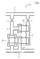
- FIGS. 1 and 2 are diagrams schematically showing the main parts of the in-vehicle electronic control device according to the present embodiment, FIG. 1 shows an electric circuit diagram, and FIG. 2 shows a component layout diagram. There is.
- FIGS. 1 and 2 a part of the power input circuit of the in-vehicle electronic control device 100 related to the EMC countermeasure circuit 1 for supporting EMC (Electromagnetic Compatibility) is extracted and shown. Electronic components such as coils, resistors, and electrolytic capacitors are not shown.
- the in-vehicle electronic control device 100 operates by receiving electric power supply from a DC power source 80 provided in the vehicle, and functions as an electronic control device mounted in the vehicle. Further, as shown in FIG. 2, the EMC countermeasure circuit 1 in the power input circuit of the in-vehicle electronic control device 100 is composed of wiring formed on the circuit board and various electronic components arranged on the circuit board. There is.
- the EMC countermeasure circuit 1 in the power input circuit includes at least two wirings of high potential side wiring 2 (first wiring) and low potential side wiring 3 (second wiring) having different potentials formed on the circuit board.
- a capacitor 10 (first capacitor) connected between the cutoff portion 6 (first fuse portion) having one end connected to the high potential side wiring 2 and the other end of the cutoff portion 6 and the low potential side wiring 3
- the capacitor 20 (second) connected between the cutoff portion 7 (second fuse portion) having one end connected to the high potential side wiring 2 and the other end of the cutoff portion 7 and the low potential side wiring 3.
- the connection 4 first connection
- the connection 5 second connection
- the high-potential side wiring 2 is connected to the high-potential side of the DC power supply 80, and the low-potential side wiring 3 is connected to the low-potential side (for example, ground level) of the DC power supply 80.
- Capacitors 10, 20, and 30 are surface mount type capacitors (for example, ceramic capacitors), and their respective electrodes are connected to land of a circuit pattern formed on a circuit board by solder or the like. It is desirable that the capacitors 10 and 20 have the same capacitance. Further, it is desirable that the capacitor 30 has the same capacitance as the capacitors 10 and 20 in order to suppress fluctuations in the noise removing ability of the EMC countermeasure circuit 1 before and after a short-circuit failure described later.
- the cutoff portion 6 and the capacitor 10 are connected in series between the high potential side wiring 2 and the low potential side wiring 3 via the connection portion 4 formed on the circuit board.
- the cutoff portion 7 and the capacitor 20 are connected in series between the high potential side wiring 2 and the low potential side wiring 3 via the connection portion 5 formed on the circuit board.
- the wiring should be as short as possible, the pattern wiring length from the high potential side wiring 2 to the low potential side wiring 3 via the capacitor 10, and the high potential side wiring 2 via the capacitor 20. It is desirable that the wiring lengths of various patterns from 1 to the low potential side wiring 3 are the same.
- the capacitor 30 is connected between the connection portion 4 and the connection portion 5. That is, one end of the capacitor 30 is connected to the cutoff portion 6 and the capacitor 10 via the connection portion 4, and the other end of the capacitor 30 is connected to the cutoff portion 7 and the capacitor 20 via the connection portion 5.
- the cutoff units 6 and 7 are formed as a circuit pattern on the circuit board, and have a fuse function of cutting off the current flow by fusing when a current of a predetermined amount or more flows.
- the wiring length can be shortened as the wiring width becomes narrower, and the substrate area can be reduced in consideration of the amount of current that allows current to flow and the amount of current that reaches fusing. It is in.
- the wiring width of the cutoff portions 6 and 7 is preferably 0.1 mm to 0.3 mm.
- the capacitors 10 and 20 function as bypass capacitors between the high potential side wiring 2 and the low potential side wiring 3.
- the capacitor 30 does not function as a bypass capacitor because charging and discharging are not performed.
- the capacitor 10 Since an abnormal situation in which a short-circuit failure occurs in the capacitor 10 due to warpage or heat shrinkage of the circuit board, for example, the high-potential side wiring 2 and the low-potential side wiring 3 pass through the capacitor 10 (and the cutoff portion 6). Is short-circuited. At this time, the current flowing through the capacitor 10 that has failed in the short circuit suddenly increases, and the cutoff portion 6 is immediately blown off by the heat generated by the increase in the current, and the increased current is cut off. Further, at the same time as the breaking of the cutoff portion 6, the capacitor 30 functions as a bypass capacitor between the high potential side wiring 2 and the low potential side wiring 3.
- the capacitors 10 and 20 connected in parallel between the high potential side wiring 2 and the low potential side wiring 3 function as bypass capacitors before the short circuit failure of the capacitor 10, and are high after the short circuit failure of the capacitor 10. Since the capacitors 20 and 30 connected in parallel between the potential side wiring 2 and the low potential side wiring 3 function as bypass capacitors, the capacitance of the bypass capacitor function fluctuates before and after the short-circuit failure of the capacitor 10. It becomes smaller.
- the capacitor 30 functions as a bypass capacitor due to the breaking portion 7 being blown by the same principle as in the case of the short-circuit failure of the capacitor 10, so that the short-circuit failure of the capacitor 20 occurs.
- the fluctuation of the electrostatic capacity of the bypass capacitor function becomes small before and after.
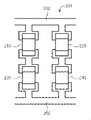
- FIG. 6 is a component layout diagram showing an EMC countermeasure circuit of the prior art as a comparative example with respect to the present embodiment.
- the capacitor 210 and the capacitor 230 are connected in series between the high potential side wiring 202 and the low potential side wiring 203 as a countermeasure against a short circuit failure.
- the capacitor 220 and the capacitor 240 are connected in series and arranged. At this time, since the combined capacitance of the capacitors connected in series is calculated by the product of the sum of the capacitances of each capacitor, it is better when two capacitors are connected in series than when there is only one capacitor. The capacitance will decrease.
- the cutoff portion 6 having one end connected to the high potential side wiring 2 and the capacitor 10 connected between the other end of the cutoff portion 6 and the low potential side wiring 3
- the cutoff portion 7 having one end connected to the high potential side wiring 2, the capacitor 20 connected between the other end of the cutoff portion 7 and the low potential side wiring 3, and the cutoff portion 6 and the capacitor 10 are connected. Since the capacitor 30 connected between the connecting portion 4, the breaking portion 7, and the connecting portion 5 to which the capacitor 20 is connected is provided, the number of capacitors can be reduced while suppressing a decrease in capacitance. Can be reduced.
- This embodiment suppresses the simultaneous short-circuit failure of the capacitors 10 and 20 in the first embodiment.
- FIG. 3 is a component layout diagram schematically showing the main parts of the in-vehicle electronic control device according to the present embodiment.
- the same members as those in the first embodiment are designated by the same reference numerals, and the description thereof will be omitted.
- the EMC countermeasure circuit 1A in the power input circuit of the in-vehicle electronic control device 100A has high potential side wiring 2 (first wiring) and low potential side wiring 3 (first wiring) having different potentials formed on the circuit board. Between at least two wirings of the second wiring), the cutoff portion 6 (first fuse portion) having one end connected to the high potential side wiring 2, and the other end of the cutoff portion 6 and the low potential side wiring 3.
- the connected capacitor 10 (first capacitor), the cutoff portion 7 (second fuse portion) having one end connected to the high potential side wiring 2, and the other end of the cutoff portion 7 and the low potential side wiring 3
- the capacitor 20 (second capacitor) connected between them, the connection part 4 (first connection part) where the cutoff part 6 and the capacitor 10 are connected, and the connection part where the cutoff part 7 and the capacitor 20 are connected. It is roughly composed of a capacitor 30 (third capacitor) connected between the fifth (second connection portion) and the capacitor 30 (third capacitor).
- the capacitor 10 and the capacitor 20 are rectangular, and the capacitor 10 and the capacitor 20 are arranged so that their longitudinal directions are different from each other. More specifically, the capacitors 10 and the capacitors 20 are mounted and arranged so as to form a right angle (90 °) in the longitudinal direction, for example.
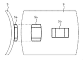
- FIG. 4 is a diagram showing an example of a case where the circuit board is warped.
- FIG. 4 illustrates a case where capacitors 9a and 9b are mounted on the circuit board 9.
- the capacitors 9a and 9b are rectangular and are arranged so that their longitudinal directions form a right angle.
- Warping of the circuit board may occur during solder mounting of electronic components, mounting of the board on the housing, thermal expansion, board division, etc.
- the circuit board 9 is warped in the direction shown in FIG. 4, that is, in the longitudinal direction of the capacitor 9a, stress is generated in the solder joint portion of the component in the mounting direction represented by the capacitor 9a. Therefore, it is conceivable that the generated stress causes cracks in the capacitor 9a, causing a short-circuit failure.
- the breaking portions 6 and 7 are blown and the capacitor 30 does not function as a bypass capacitor. Therefore, the EMC countermeasure circuit 1 Noise resistance is reduced.
- the capacitors 10 and the capacitors 20 are arranged so as to be in different directions in the longitudinal direction, it is possible to prevent the capacitors 10 and 20 from causing short-circuit failures at the same time due to the warp in one direction of the circuit board. can do.
- An effective mounting direction for suppressing the simultaneous occurrence of short-circuit failures is to align the longitudinal direction of the board and the longitudinal direction of the capacitor when the board has different vertical and horizontal lengths such as a rectangle. It is preferable to provide a mounting device so that the longitudinal direction of the substrate and the longitudinal direction of the capacitor form 90 ° (perpendicular). That is, it is desirable to provide a capacitor that is mounted so that the longitudinal direction of the capacitor is aligned with respect to the direction in which warpage is likely to occur due to the shape of the substrate, and a capacitor that is mounted so as to form a 90 ° (right angle) with respect to the longitudinal direction of the capacitor.
- This embodiment suppresses the influence of a short-circuit failure in the capacitor 30 in the first and second embodiments.
- FIG. 5 is a component layout diagram schematically showing a main part of an in-vehicle electronic control device according to the present embodiment.
- the same members as those in the first and second embodiments are designated by the same reference numerals, and the description thereof will be omitted.
- the circuits having the configurations shown in the first embodiment and the second embodiment are divided into the high potential side wiring 2 and the low potential side wiring.
- a plurality of for example, two in this embodiment are connected in parallel with the third.
- the EMC countermeasure circuit 1B in the power input circuit of the in-vehicle electronic control device 100B according to the present embodiment is low with the high potential side wiring 2 (first wiring) having different potentials formed on the circuit board.
- a capacitor 21 (second capacitor) connected between the potential side wiring 3, a connection portion 41 (first connection portion) to which the cutoff portion 61 and the capacitor 11 are connected, the cutoff portion 71, and the capacitor 21.
- Capacitor 31 (third capacitor) connected between the connection part 51 (second connection part) to which is connected, and cutoff part 62 (third fuse) whose one end is connected to the high potential side wiring 2.
- a capacitor 12 (fourth capacitor) connected between the other end of the cutoff part 62 and the low potential side wiring 3, and a cutoff part 72 (fourth part) having one end connected to the high potential side wiring 2.
- the capacitor 22 (fifth capacitor) connected between the other end of the cutoff portion 72 and the low potential side wiring 3, and the connection portion 42 (the connection portion 42) to which the cutoff portion 62 and the capacitor 12 are connected. It is roughly composed of a capacitor 32 (sixth capacitor) connected between the connection portion 52 (fourth connection portion) to which the third connection portion), the cutoff portion 72, and the capacitor 22 are connected. ..
- the capacitor 11 and the capacitor 21 are rectangular, and the capacitor 11 and the capacitor 21 are arranged so that their longitudinal directions are different from each other. More specifically, the capacitors 11 and the capacitors 21 are mounted and arranged so as to form a right angle (90 °) in the longitudinal direction, for example.
- the capacitor 12 and the capacitor 22 are rectangular, and the capacitor 12 and the capacitor 22 are arranged so that their longitudinal directions are different from each other. More specifically, the capacitors 12 and the capacitors 22 are mounted and arranged so as to form a right angle (90 °) in the longitudinal direction, for example.
- the capacitor 31 and the capacitor 32 are rectangular, and the capacitor 31 and the capacitor 32 are arranged so that their longitudinal directions are different from each other. More specifically, the capacitors 31 and the capacitors 32 are mounted and arranged so as to form a right angle (90 °) in the longitudinal direction, for example.
- the capacitors 10 and 20 are configured to have different longitudinal directions to prevent short-circuit failures from occurring in the capacitors 10 and 20 at the same time.
- short-circuit failures may occur in the capacitors 20 and 30 at the same time.
- the noise immunity is lowered.
- a plurality of circuits having the configurations shown in the first embodiment and the second embodiment are connected in parallel between the high potential side wiring 2 and the low potential side wiring 3.
- a short circuit failure may occur in many capacitors at the same time, and in this case, the noise immunity is extremely lowered.
- the capacitor 11 and the capacitor 21 are arranged so as to be in different directions in the longitudinal direction, and the capacitor 12 and the capacitor 22 are arranged so as to be in different directions in the longitudinal direction, and the capacitor 31 and the capacitor are arranged in different directions. Since the 32 are arranged so that the longitudinal directions are different, the short-circuit failures of the capacitors 11 and 21 occur at the same time, the short-circuit failures of the capacitors 12 and 22 occur at the same time, and the short-circuit failures of the capacitors 12 and 22 occur simultaneously with respect to the warp in one direction of the circuit board. It is possible to suppress the simultaneous occurrence of short-circuit failures of the capacitors 31 and 32. That is, in the present embodiment, it is possible to suppress the simultaneous occurrence of short-circuit failures of a large number of capacitors due to the warp direction of the substrate, and it is possible to suppress an extreme decrease in noise immunity.
- the capacitors are arranged. It is possible to suppress a decrease in noise immunity due to a short circuit failure.
- the present invention is not limited to the above embodiment, and includes various modifications and combinations within a range not deviating from the gist thereof.
- a cutoff portion (cutoff portion 6,7,61,62,71,72) is connected to the high potential side wiring 2, and a capacitor is connected to the low potential side wiring 3.
- the capacitor is connected to the high potential side wiring 2 and the cutoff portion is connected to the low potential side wiring 3. It may be configured.
- the present invention is not limited to the one including all the configurations described in the above-described embodiment, and includes the one in which a part of the configurations is deleted.
- each of the above configurations, functions and the like may be realized by designing a part or all of them by, for example, an integrated circuit.
- each of the above configurations, functions, and the like may be realized by software by the processor interpreting and executing a program that realizes each function.
Landscapes
- Engineering & Computer Science (AREA)
- Microelectronics & Electronic Packaging (AREA)
- Mechanical Engineering (AREA)
- Physics & Mathematics (AREA)
- Electromagnetism (AREA)
- Structures For Mounting Electric Components On Printed Circuit Boards (AREA)
- Structure Of Printed Boards (AREA)
Abstract
Description
本発明の第1の実施の形態を図1及び図2を参照しつつ説明する。
本発明の第2の実施の形態を図3及び図4を参照しつつ説明する。
本発明の第3の実施の形態を図5を参照しつつ説明する。
なお、本発明は上記の実施の形態に限定されるものではなく、その要旨を逸脱しない範囲内の様々な変形例や組み合わせが含まれる。
Claims (4)
- 直流電源からの電力供給を受けて動作する車載用電子制御装置であって、
基板上に形成された電位の異なる第一の配線及び第二の配線の少なくとも2つの配線と、
前記第一の配線に一端が接続された第一のヒューズ部と、
前記第一のヒューズ部の他端と前記第二の配線との間に接続された第一のコンデンサと、
前記第一の配線に一端が接続された第二のヒューズ部と、
前記第二のヒューズ部の他端と前記第二の配線との間に接続された第二のコンデンサと
を備えたことを特徴とする車載用電子制御装置。 - 請求項1記載の車載用電子制御装置において、
前記第一のヒューズ部と前記第一のコンデンサとが接続される第一の接続部と前記第二のヒューズ部と前記第二のコンデンサとが接続される第二の接続部との間に接続された第三のコンデンサをさらに備えたことを特徴とする車載用電子制御装置。 - 請求項2記載の車載用電子制御装置において、
前記第一のコンデンサおよび前記第二のコンデンサは長方形であって、
前記第一のコンデンサと前記第二のコンデンサは、それぞれの長手方向が異なる向きとなるように配置されたことを特徴とする車載用電子制御装置。 - 請求項2記載の車載用電子制御装置において、
前記第一の配線に一端が接続された第三のヒューズ部と、
前記第三のヒューズ部の他端と前記第二の配線との間に接続された第四のコンデンサと、
前記第一の配線に一端が接続された第四のヒューズ部と、
前記第四のヒューズ部の他端と前記第二の配線との間に接続された第五のコンデンサと、
前記第三のヒューズ部と前記第四のコンデンサとが接続される第三の接続部と前記第四のヒューズ部と前記第五のコンデンサとが接続される第四の接続部との間に接続された第六のコンデンサとを備え、
前記第三のコンデンサおよび前記第六のコンデンサは長方形であって、
前記第三のコンデンサと前記第六のコンデンサは、それぞれの長手方向が異なる向きとなるように配置されたことを特徴とする車載用電子制御装置。
Priority Applications (3)
| Application Number | Priority Date | Filing Date | Title |
|---|---|---|---|
| US18/252,903 US12432845B2 (en) | 2020-12-25 | 2021-08-31 | Vehicle-mounted electronic control device |
| JP2022571043A JP7539491B2 (ja) | 2020-12-25 | 2021-08-31 | 車載用電子制御装置 |
| CN202180080706.1A CN116529126A (zh) | 2020-12-25 | 2021-08-31 | 车载用电子控制装置 |
Applications Claiming Priority (2)
| Application Number | Priority Date | Filing Date | Title |
|---|---|---|---|
| JP2020-217711 | 2020-12-25 | ||
| JP2020217711 | 2020-12-25 |
Publications (1)
| Publication Number | Publication Date |
|---|---|
| WO2022137652A1 true WO2022137652A1 (ja) | 2022-06-30 |
Family
ID=82158933
Family Applications (1)
| Application Number | Title | Priority Date | Filing Date |
|---|---|---|---|
| PCT/JP2021/031893 Ceased WO2022137652A1 (ja) | 2020-12-25 | 2021-08-31 | 車載用電子制御装置 |
Country Status (4)
| Country | Link |
|---|---|
| US (1) | US12432845B2 (ja) |
| JP (1) | JP7539491B2 (ja) |
| CN (1) | CN116529126A (ja) |
| WO (1) | WO2022137652A1 (ja) |
Families Citing this family (1)
| Publication number | Priority date | Publication date | Assignee | Title |
|---|---|---|---|---|
| CN116529126A (zh) * | 2020-12-25 | 2023-08-01 | 日立安斯泰莫株式会社 | 车载用电子控制装置 |
Citations (3)
| Publication number | Priority date | Publication date | Assignee | Title |
|---|---|---|---|---|
| JPH06283665A (ja) * | 1992-12-17 | 1994-10-07 | Internatl Business Mach Corp <Ibm> | 自己保護型デカップリング・コンデンサ |
| JPH11346061A (ja) * | 1998-06-02 | 1999-12-14 | Hitachi Ltd | コンデンサ内蔵回路基板およびその製造方法 |
| JP2004241506A (ja) * | 2003-02-04 | 2004-08-26 | Denso Corp | 車両用配線板 |
Family Cites Families (48)
| Publication number | Priority date | Publication date | Assignee | Title |
|---|---|---|---|---|
| US3699395A (en) * | 1970-01-02 | 1972-10-17 | Rca Corp | Semiconductor devices including fusible elements |
| US3835294A (en) * | 1973-04-06 | 1974-09-10 | Binks Mfg Co | High pressure electric fluid heater |
| US4002949A (en) * | 1975-11-13 | 1977-01-11 | Kearney-National, Inc. | Transformer protective system |
| US4272753A (en) * | 1978-08-16 | 1981-06-09 | Harris Corporation | Integrated circuit fuse |
| US4394639A (en) * | 1978-12-18 | 1983-07-19 | Mcgalliard James D | Printed circuit fuse assembly |
| US4491860A (en) * | 1982-04-23 | 1985-01-01 | Signetics Corporation | TiW2 N Fusible links in semiconductor integrated circuits |
| US4626818A (en) * | 1983-11-28 | 1986-12-02 | Centralab, Inc. | Device for programmable thick film networks |
| US4582659A (en) * | 1983-11-28 | 1986-04-15 | Centralab, Inc. | Method for manufacturing a fusible device for use in a programmable thick film network |
| US4652974A (en) * | 1985-10-28 | 1987-03-24 | International Business Machines Corporation | Method and structure for effecting engineering changes in a multiple device module package |
| US4670813A (en) * | 1985-11-29 | 1987-06-02 | The Perkin-Elmer Corporation | Programmable lamp plug |
| US5014002A (en) * | 1989-04-18 | 1991-05-07 | Vlsi Technology, Inc. | ATE jumper programmable interface board |
| US5311053A (en) * | 1991-06-12 | 1994-05-10 | Aptix Corporation | Interconnection network |
| US5808351A (en) * | 1994-02-08 | 1998-09-15 | Prolinx Labs Corporation | Programmable/reprogramable structure using fuses and antifuses |
| US5572409A (en) * | 1994-02-08 | 1996-11-05 | Prolinx Labs Corporation | Apparatus including a programmable socket adapter for coupling an electronic component to a component socket on a printed circuit board |
| US5625299A (en) * | 1995-02-03 | 1997-04-29 | Uhling; Thomas F. | Multiple lead analog voltage probe with high signal integrity over a wide band width |
| JP3661725B2 (ja) * | 1996-12-20 | 2005-06-22 | 旭硝子株式会社 | 電源装置 |
| JP2005123376A (ja) * | 2003-10-16 | 2005-05-12 | Toshiba Corp | 半導体装置及びその製造方法 |
| US20060120005A1 (en) * | 2004-11-15 | 2006-06-08 | Van Sickle Robert J | Transient voltage surge suppression systems |
| JP4956020B2 (ja) * | 2005-03-02 | 2012-06-20 | パナソニック株式会社 | 点灯ユニット及び放電ランプ |
| DE102005024347B8 (de) * | 2005-05-27 | 2010-07-08 | Infineon Technologies Ag | Elektrisches Bauteil mit abgesichertem Stromzuführungsanschluss |
| DE102005024346B4 (de) * | 2005-05-27 | 2012-04-26 | Infineon Technologies Ag | Sicherungselement mit Auslöseunterstützung |
| KR20070112644A (ko) * | 2006-05-22 | 2007-11-27 | 삼성전자주식회사 | 어레이 기판, 이를 갖는 액정표시장치, 및 이의 검사 방법 |
| WO2010106652A1 (ja) * | 2009-03-18 | 2010-09-23 | 東芝三菱電機産業システム株式会社 | 無停電電源装置 |
| US8022641B2 (en) * | 2009-05-01 | 2011-09-20 | Focal Point, L.L.C. | Recessed LED down light |
| CN201898335U (zh) * | 2010-12-11 | 2011-07-13 | 巨石集团有限公司 | 手自动阶梯式冗余电容补偿装置 |
| JP5583042B2 (ja) * | 2011-02-04 | 2014-09-03 | 株式会社デンソー | 電子制御装置 |
| JP2013232620A (ja) * | 2012-01-27 | 2013-11-14 | Rohm Co Ltd | チップ部品 |
| US9025311B1 (en) * | 2012-04-25 | 2015-05-05 | Kemet Electronics Corporation | Very large ceramic capacitor with mechanical shock resistance |
| GB2506154B (en) * | 2012-09-21 | 2015-03-18 | Control Tech Ltd | DC Link Capacitor Bank |
| CN110504257B (zh) * | 2012-11-02 | 2023-12-08 | 罗姆股份有限公司 | 片状电容器、电路组件以及电子设备 |
| JP2014239207A (ja) * | 2013-05-10 | 2014-12-18 | 株式会社村田製作所 | コンデンサ素子の実装構造体およびコンデンサ素子の実装方法 |
| CN105473930B (zh) * | 2013-08-23 | 2019-03-19 | 莫列斯有限公司 | Led模块 |
| CN203574370U (zh) * | 2013-10-29 | 2014-04-30 | 北京精密机电控制设备研究所 | 一种电源滤波储能电路 |
| US9773588B2 (en) * | 2014-05-16 | 2017-09-26 | Rohm Co., Ltd. | Chip parts |
| KR101533996B1 (ko) * | 2014-10-23 | 2015-07-06 | 주식회사 에스엠하이테크 | 온도 퓨즈 기능을 가진 smd형 마이크로 복합 퓨즈 및 그 제조방법 |
| JP2016143845A (ja) | 2015-02-05 | 2016-08-08 | 株式会社デンソー | 車載用電子制御装置 |
| WO2016161042A1 (en) * | 2015-03-30 | 2016-10-06 | Parallel Wireless, Inc. | Power management for vehicle-mounted base station |
| JP2017061180A (ja) * | 2015-09-24 | 2017-03-30 | 株式会社オートネットワーク技術研究所 | 車載用電源装置 |
| US9729188B2 (en) * | 2015-09-25 | 2017-08-08 | Electrochem Solutions, Inc. | Protecting wireless communication components in a highly resonant field |
| JP6540565B2 (ja) * | 2016-03-16 | 2019-07-10 | 株式会社オートネットワーク技術研究所 | 車両用電源供給システム、車両用駆動システム |
| JP6732633B2 (ja) * | 2016-11-07 | 2020-07-29 | 株式会社ジャパンディスプレイ | 電子機器及び表示装置 |
| JP6459087B2 (ja) * | 2017-03-17 | 2019-01-30 | 株式会社ケーヒン | 回路保護装置及び電圧検出装置 |
| US10707145B2 (en) * | 2017-09-08 | 2020-07-07 | Kemet Electronics Corporation | High density multi-component packages |
| US10681814B2 (en) * | 2017-09-08 | 2020-06-09 | Kemet Electronics Corporation | High density multi-component packages |
| US10178770B1 (en) * | 2017-12-22 | 2019-01-08 | Kemet Electronics Corporation | Higher density multi-component and serial packages |
| CN122294376A (zh) * | 2018-11-07 | 2026-06-26 | 京瓷Avx元器件公司 | 具有配置用于视觉检查的端子的表面安装薄膜元件 |
| JP7363599B2 (ja) * | 2020-03-09 | 2023-10-18 | トヨタ自動車株式会社 | 車両用電源システム |
| CN116529126A (zh) * | 2020-12-25 | 2023-08-01 | 日立安斯泰莫株式会社 | 车载用电子控制装置 |
-
2021
- 2021-08-31 CN CN202180080706.1A patent/CN116529126A/zh active Pending
- 2021-08-31 JP JP2022571043A patent/JP7539491B2/ja active Active
- 2021-08-31 WO PCT/JP2021/031893 patent/WO2022137652A1/ja not_active Ceased
- 2021-08-31 US US18/252,903 patent/US12432845B2/en active Active
Patent Citations (3)
| Publication number | Priority date | Publication date | Assignee | Title |
|---|---|---|---|---|
| JPH06283665A (ja) * | 1992-12-17 | 1994-10-07 | Internatl Business Mach Corp <Ibm> | 自己保護型デカップリング・コンデンサ |
| JPH11346061A (ja) * | 1998-06-02 | 1999-12-14 | Hitachi Ltd | コンデンサ内蔵回路基板およびその製造方法 |
| JP2004241506A (ja) * | 2003-02-04 | 2004-08-26 | Denso Corp | 車両用配線板 |
Also Published As
| Publication number | Publication date |
|---|---|
| JP7539491B2 (ja) | 2024-08-23 |
| JPWO2022137652A1 (ja) | 2022-06-30 |
| US20230422391A1 (en) | 2023-12-28 |
| CN116529126A (zh) | 2023-08-01 |
| US12432845B2 (en) | 2025-09-30 |
Similar Documents
| Publication | Publication Date | Title |
|---|---|---|
| CN100568658C (zh) | 用于静电放电抑制的装置和系统 | |
| US9748155B2 (en) | Printed circuit board | |
| JPH02187093A (ja) | 印刷配線板 | |
| US9368309B2 (en) | Electronic part and electronic control unit | |
| CN107275165B (zh) | 包括中断布线的电子控制装置 | |
| US20210307216A1 (en) | Electronic Control Device | |
| JP7539491B2 (ja) | 車載用電子制御装置 | |
| JP6672605B2 (ja) | 電力変換装置 | |
| US8125794B2 (en) | Multilayer printed wiring board and electronic device using the same | |
| JP2002131333A (ja) | プローブカード | |
| JP4710496B2 (ja) | 回路基板及び電子回路装置 | |
| CN114747302B (zh) | 改进稳定性的电阻性pcb迹线 | |
| JP2014090042A (ja) | 電子制御ユニットの耐静電気構造 | |
| US7557302B2 (en) | Printed circuit board with electrostatic discharge damage prevention | |
| JP2011243878A (ja) | 集合基板 | |
| JP4900264B2 (ja) | 電子制御ユニットの耐静電気構造 | |
| JP2016143845A (ja) | 車載用電子制御装置 | |
| JP6373912B2 (ja) | ノイズフィルタ、及び当該ノイズフィルタが形成された回路基板 | |
| JP4872877B2 (ja) | 配線基板 | |
| JPH04192389A (ja) | 電子回路 | |
| JP6362419B2 (ja) | プリント回路基板 | |
| JP4968299B2 (ja) | 電気機器 | |
| JP2001035632A (ja) | プリント基板装置及びその製造方法 | |
| JP2017076702A (ja) | プリント配線基板 | |
| JP6499552B2 (ja) | 雑音耐性の高い回路基板及び電子装置 |
Legal Events
| Date | Code | Title | Description |
|---|---|---|---|
| 121 | Ep: the epo has been informed by wipo that ep was designated in this application |
Ref document number: 21909810 Country of ref document: EP Kind code of ref document: A1 |
|
| ENP | Entry into the national phase |
Ref document number: 2022571043 Country of ref document: JP Kind code of ref document: A |
|
| WWE | Wipo information: entry into national phase |
Ref document number: 18252903 Country of ref document: US |
|
| WWE | Wipo information: entry into national phase |
Ref document number: 202180080706.1 Country of ref document: CN |
|
| NENP | Non-entry into the national phase |
Ref country code: DE |
|
| 122 | Ep: pct application non-entry in european phase |
Ref document number: 21909810 Country of ref document: EP Kind code of ref document: A1 |
|
| WWG | Wipo information: grant in national office |
Ref document number: 18252903 Country of ref document: US |