WO2022131337A1 - セラミック板及びその製造方法、複合基板及びその製造方法、並びに、回路基板及びその製造方法 - Google Patents
セラミック板及びその製造方法、複合基板及びその製造方法、並びに、回路基板及びその製造方法 Download PDFInfo
- Publication number
- WO2022131337A1 WO2022131337A1 PCT/JP2021/046552 JP2021046552W WO2022131337A1 WO 2022131337 A1 WO2022131337 A1 WO 2022131337A1 JP 2021046552 W JP2021046552 W JP 2021046552W WO 2022131337 A1 WO2022131337 A1 WO 2022131337A1
- Authority
- WO
- WIPO (PCT)
- Prior art keywords
- main surface
- scribe line
- ceramic plate
- ceramic
- hole
- Prior art date
- Legal status (The legal status is an assumption and is not a legal conclusion. Google has not performed a legal analysis and makes no representation as to the accuracy of the status listed.)
- Ceased
Links
Images





Classifications
-
- H—ELECTRICITY
- H05—ELECTRIC TECHNIQUES NOT OTHERWISE PROVIDED FOR
- H05K—PRINTED CIRCUITS; CASINGS OR CONSTRUCTIONAL DETAILS OF ELECTRIC APPARATUS; MANUFACTURE OF ASSEMBLAGES OF ELECTRICAL COMPONENTS
- H05K1/00—Printed circuits
- H05K1/02—Details
-
- H—ELECTRICITY
- H05—ELECTRIC TECHNIQUES NOT OTHERWISE PROVIDED FOR
- H05K—PRINTED CIRCUITS; CASINGS OR CONSTRUCTIONAL DETAILS OF ELECTRIC APPARATUS; MANUFACTURE OF ASSEMBLAGES OF ELECTRICAL COMPONENTS
- H05K3/00—Apparatus or processes for manufacturing printed circuits
-
- H—ELECTRICITY
- H05—ELECTRIC TECHNIQUES NOT OTHERWISE PROVIDED FOR
- H05K—PRINTED CIRCUITS; CASINGS OR CONSTRUCTIONAL DETAILS OF ELECTRIC APPARATUS; MANUFACTURE OF ASSEMBLAGES OF ELECTRICAL COMPONENTS
- H05K3/00—Apparatus or processes for manufacturing printed circuits
- H05K3/02—Apparatus or processes for manufacturing printed circuits in which the conductive material is applied to the surface of the insulating support and is thereafter removed from such areas of the surface which are not intended for current conducting or shielding
- H05K3/06—Apparatus or processes for manufacturing printed circuits in which the conductive material is applied to the surface of the insulating support and is thereafter removed from such areas of the surface which are not intended for current conducting or shielding the conductive material being removed chemically or electrolytically, e.g. by photo-etch process
Definitions
- This disclosure relates to a ceramic plate and its manufacturing method, a composite substrate and its manufacturing method, and a circuit board and its manufacturing method.
- the ceramic plate may have one or a plurality of compartments partitioned by a plurality of scribe lines, and an outer peripheral portion including an outer edge of a main surface surrounding the one or a plurality of compartments.
- the outer peripheral portion can be used as a handle, for example.
- the compartment can be used, for example, as a ceramic member of a circuit board.
- the ceramic member included in the circuit board described above is obtained by dividing the ceramic plate described above. Therefore, it is possible to sufficiently suppress the occurrence of cracks, chips and burrs of the ceramic member. Further, since a part of the inner wall surface of the through hole forms a corner portion of the ceramic member, chamfering can be omitted. Therefore, it is possible to suppress the occurrence of cracks, chips and burrs due to chamfering.
- the present disclosure discloses, in one aspect, a step of joining a ceramic plate manufactured by the above manufacturing method and a metal plate, and a step of removing a part of the metal plate to form a conductor portion on the main surface of the ceramic plate.
- a method for manufacturing a composite substrate is provided.
- the circuit board obtained by this manufacturing method is obtained by dividing the above-mentioned ceramic plate. Therefore, it is possible to sufficiently suppress the occurrence of cracks, chips and burrs of the ceramic member. Further, since a part of the inner wall surface of the through hole forms a corner portion of the ceramic member, chamfering can be omitted. Therefore, it is possible to suppress the occurrence of cracks, chips and burrs due to chamfering.
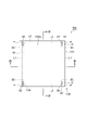
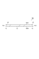
- FIG. 2, FIGS. 3 and 4 show an example in which the first scribe line L1 and the second scribe line L2 are formed only on one main surface 100A of the ceramic plate 100, but the present invention is not limited thereto. .. That is, the first scribe line L1 and the second scribe line L2 may also be formed on the main surface 100B on the opposite side of the main surface 100A of the ceramic plate 100.
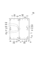
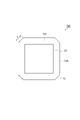
- FIG. 6 is a plan view of the ceramic plate according to another embodiment.
- the ceramic plate 105 shown in FIG. 6 has a flat plate shape.
- the main surface 105A of the ceramic plate 105 is rectangular and is divided into a plurality of parts by a first scribe line L1 and a second scribe line L2 extending in different directions from each other.
- the main surface 105A is formed with three first scribe lines L1 extending in the first direction and three second scribe lines L2 extending in the second direction orthogonal to the first direction. ..
- the three first scribe lines L1 are parallel to each other, and the three second scribe lines L2 are also parallel to each other.
- the first scribe line L1 and the second scribe line L2 are orthogonal to each other.
- the first through hole 50 which penetrates in the direction orthogonal to the main surface 105A (thickness direction of the ceramic plate 105),
- the second through hole 50A and the third through hole 50B are formed.
- the first through hole 50 is formed in the corner portion 102 of the ceramic plate 105.
- a second through hole 50A is formed between the two first through holes 50 provided in the two adjacent corner portions 102.
- the edge of the second through hole 50A on the main surface 105A has a triangular shape (isosceles triangle shape).
- the main surface may be partitioned by a first scribe line L1 and a second scribe line L2 so that six or more ceramic members can be obtained.
- the thickness of the ceramic plates 100 and 105 may be 0.1 to 0.5 mm, and may be 0.15 to 0.4 mm. If the thickness becomes too large, it tends to take time to form the first through hole 50, the second through hole 50A, and the third through hole 50B. On the other hand, if the thickness becomes too small, the strength of the ceramic plates 100 and 105 tends to decrease.
- the opening area of the first through hole 50 may be, for example, 3 to 30 mm 2 or 5 to 20 mm 2 .
- the opening area of the second through hole 50A may be, for example, 6 to 60 mm 2 or 10 to 40 mm 2 .
- the opening area of the third through hole 50B may be, for example, 12 to 120 mm 2 or 20 to 80 mm 2 .
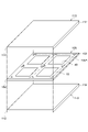
- the bonding substrate 200 includes a pair of metal plates 110 arranged so as to face each other, and a ceramic plate 105 between the pair of metal plates 110.
- the pair of metal plates 110 are joined to the ceramic plate 105 so as to cover the main surface 105A and the main surface 105B of the ceramic plate 105.
- Examples of the metal plate 110 include a copper plate.
- the shape and size of the ceramic plate 105 and the metal plate 110 may be the same or different.
- the bonded substrate 200 can be manufactured by the above-mentioned manufacturing method.
Landscapes
- Engineering & Computer Science (AREA)
- Microelectronics & Electronic Packaging (AREA)
- Manufacturing & Machinery (AREA)
- Structure Of Printed Boards (AREA)
Priority Applications (1)
| Application Number | Priority Date | Filing Date | Title |
|---|---|---|---|
| JP2022542066A JPWO2022131337A1 (https=) | 2020-12-17 | 2021-12-16 |
Applications Claiming Priority (2)
| Application Number | Priority Date | Filing Date | Title |
|---|---|---|---|
| JP2020209383 | 2020-12-17 | ||
| JP2020-209383 | 2020-12-17 |
Publications (1)
| Publication Number | Publication Date |
|---|---|
| WO2022131337A1 true WO2022131337A1 (ja) | 2022-06-23 |
Family
ID=82059572
Family Applications (1)
| Application Number | Title | Priority Date | Filing Date |
|---|---|---|---|
| PCT/JP2021/046552 Ceased WO2022131337A1 (ja) | 2020-12-17 | 2021-12-16 | セラミック板及びその製造方法、複合基板及びその製造方法、並びに、回路基板及びその製造方法 |
Country Status (2)
| Country | Link |
|---|---|
| JP (1) | JPWO2022131337A1 (https=) |
| WO (1) | WO2022131337A1 (https=) |
Citations (5)
| Publication number | Priority date | Publication date | Assignee | Title |
|---|---|---|---|---|
| JPH0348259U (https=) * | 1989-09-18 | 1991-05-08 | ||
| JPH0566999U (ja) * | 1992-02-21 | 1993-09-03 | 昭和電工株式会社 | 回路用基板 |
| JP2000114411A (ja) * | 1998-10-09 | 2000-04-21 | Sumitomo Metal Electronics Devices Inc | セラミックパッケ−ジの製造方法 |
| JP2005136172A (ja) * | 2003-10-30 | 2005-05-26 | Kyocera Corp | 多数個取り配線基板 |
| JP2013010644A (ja) * | 2011-06-28 | 2013-01-17 | Mitsuboshi Diamond Industrial Co Ltd | ガラス基板のスクライブ方法 |
Family Cites Families (3)
| Publication number | Priority date | Publication date | Assignee | Title |
|---|---|---|---|---|
| JP4795573B2 (ja) * | 2001-07-16 | 2011-10-19 | 株式会社東芝 | セラミックス回路基板 |
| JP5574804B2 (ja) * | 2010-04-27 | 2014-08-20 | 京セラ株式会社 | 多数個取り配線基板 |
| JP6317115B2 (ja) * | 2014-01-21 | 2018-04-25 | 京セラ株式会社 | 多数個取り配線基板、配線基板および多数個取り配線基板の製造方法 |
-
2021
- 2021-12-16 WO PCT/JP2021/046552 patent/WO2022131337A1/ja not_active Ceased
- 2021-12-16 JP JP2022542066A patent/JPWO2022131337A1/ja active Pending
Patent Citations (5)
| Publication number | Priority date | Publication date | Assignee | Title |
|---|---|---|---|---|
| JPH0348259U (https=) * | 1989-09-18 | 1991-05-08 | ||
| JPH0566999U (ja) * | 1992-02-21 | 1993-09-03 | 昭和電工株式会社 | 回路用基板 |
| JP2000114411A (ja) * | 1998-10-09 | 2000-04-21 | Sumitomo Metal Electronics Devices Inc | セラミックパッケ−ジの製造方法 |
| JP2005136172A (ja) * | 2003-10-30 | 2005-05-26 | Kyocera Corp | 多数個取り配線基板 |
| JP2013010644A (ja) * | 2011-06-28 | 2013-01-17 | Mitsuboshi Diamond Industrial Co Ltd | ガラス基板のスクライブ方法 |
Also Published As
| Publication number | Publication date |
|---|---|
| JPWO2022131337A1 (https=) | 2022-06-23 |
Similar Documents
| Publication | Publication Date | Title |
|---|---|---|
| CN1938837B (zh) | 在无源电子元件衬底上形成划线的方法 | |
| US7833370B2 (en) | Method for manufacturing a ceramic multi-layered substrate | |
| JP2761776B2 (ja) | 多層回路板の製造方法 | |
| JP7465879B2 (ja) | セラミックス基板及びその製造方法、複合基板及びその製造方法、並びに、回路基板及びその製造方法 | |
| CN102687599A (zh) | 多个组合式配线基板及其制造方法、以及配线基板及其制造方法 | |
| KR20150126845A (ko) | 파워 모듈용 기판의 제조 방법 | |
| JP6853455B2 (ja) | パワーモジュール用基板の製造方法 | |
| JPH06170822A (ja) | シート加工品及びその製造方法 | |
| WO2021085490A1 (ja) | セラミックス基板及びその製造方法、複合基板及びその製造方法、並びに、回路基板及びその製造方法 | |
| KR20050036775A (ko) | 적층전자부품의 제조방법 | |
| WO2022131337A1 (ja) | セラミック板及びその製造方法、複合基板及びその製造方法、並びに、回路基板及びその製造方法 | |
| JP6201761B2 (ja) | パワーモジュール用基板の製造方法 | |
| JP7573023B2 (ja) | 窒化ケイ素板及びその製造方法、複合基板及びその製造方法、並びに、回路基板及びその製造方法 | |
| WO2022045140A1 (ja) | セラミック板及びその製造方法、接合基板及びその製造方法、並びに、回路基板及びその製造方法 | |
| JP4881557B2 (ja) | チップ抵抗器の製造方法 | |
| JP7621339B2 (ja) | 窒化アルミニウム板及びその製造方法、複合基板及びその製造方法、並びに、回路基板及びその製造方法 | |
| JP7490934B2 (ja) | 回路基板の製造方法及び回路基板 | |
| JP2008041945A (ja) | パワーモジュール用基板の製造方法およびパワーモジュール用基板並びにパワーモジュール | |
| WO2022172900A1 (ja) | セラミック板及びその製造方法、並びに、回路基板及びその製造方法 | |
| WO2022176716A1 (ja) | セラミック板、及びセラミック板の製造方法 | |
| JP7615769B2 (ja) | 絶縁回路基板の製造方法 | |
| KR102429043B1 (ko) | 세라믹 기판 제조 방법 | |
| KR102429042B1 (ko) | 세라믹 기판 제조 방법 | |
| JP7484109B2 (ja) | 窒化珪素セラミックス焼結基板の製造方法及び回路基板の製造方法 | |
| JP2012142490A (ja) | マーキング方法 |
Legal Events
| Date | Code | Title | Description |
|---|---|---|---|
| ENP | Entry into the national phase |
Ref document number: 2022542066 Country of ref document: JP Kind code of ref document: A |
|
| 121 | Ep: the epo has been informed by wipo that ep was designated in this application |
Ref document number: 21906697 Country of ref document: EP Kind code of ref document: A1 |
|
| NENP | Non-entry into the national phase |
Ref country code: DE |
|
| 122 | Ep: pct application non-entry in european phase |
Ref document number: 21906697 Country of ref document: EP Kind code of ref document: A1 |