WO2022131059A1 - 半導体素子の製造方法、半導体素子及び半導体装置 - Google Patents
半導体素子の製造方法、半導体素子及び半導体装置 Download PDFInfo
- Publication number
- WO2022131059A1 WO2022131059A1 PCT/JP2021/044789 JP2021044789W WO2022131059A1 WO 2022131059 A1 WO2022131059 A1 WO 2022131059A1 JP 2021044789 W JP2021044789 W JP 2021044789W WO 2022131059 A1 WO2022131059 A1 WO 2022131059A1
- Authority
- WO
- WIPO (PCT)
- Prior art keywords
- semiconductor
- semiconductor element
- gan layer
- manufacturing
- mask
- Prior art date
- Legal status (The legal status is an assumption and is not a legal conclusion. Google has not performed a legal analysis and makes no representation as to the accuracy of the status listed.)
- Ceased
Links
Images




Classifications
-
- H—ELECTRICITY
- H10—SEMICONDUCTOR DEVICES; ELECTRIC SOLID-STATE DEVICES NOT OTHERWISE PROVIDED FOR
- H10D—INORGANIC ELECTRIC SEMICONDUCTOR DEVICES
- H10D8/00—Diodes
- H10D8/01—Manufacture or treatment
- H10D8/051—Manufacture or treatment of Schottky diodes
-
- H—ELECTRICITY
- H10—SEMICONDUCTOR DEVICES; ELECTRIC SOLID-STATE DEVICES NOT OTHERWISE PROVIDED FOR
- H10D—INORGANIC ELECTRIC SEMICONDUCTOR DEVICES
- H10D62/00—Semiconductor bodies, or regions thereof, of devices having potential barriers
- H10D62/10—Shapes, relative sizes or dispositions of the regions of the semiconductor bodies; Shapes of the semiconductor bodies
- H10D62/113—Isolations within a component, i.e. internal isolations
- H10D62/115—Dielectric isolations, e.g. air gaps
-
- H—ELECTRICITY
- H10—SEMICONDUCTOR DEVICES; ELECTRIC SOLID-STATE DEVICES NOT OTHERWISE PROVIDED FOR
- H10D—INORGANIC ELECTRIC SEMICONDUCTOR DEVICES
- H10D62/00—Semiconductor bodies, or regions thereof, of devices having potential barriers
- H10D62/10—Shapes, relative sizes or dispositions of the regions of the semiconductor bodies; Shapes of the semiconductor bodies
- H10D62/117—Shapes of semiconductor bodies
-
- H—ELECTRICITY
- H10—SEMICONDUCTOR DEVICES; ELECTRIC SOLID-STATE DEVICES NOT OTHERWISE PROVIDED FOR
- H10D—INORGANIC ELECTRIC SEMICONDUCTOR DEVICES
- H10D62/00—Semiconductor bodies, or regions thereof, of devices having potential barriers
- H10D62/80—Semiconductor bodies, or regions thereof, of devices having potential barriers characterised by the materials
- H10D62/85—Semiconductor bodies, or regions thereof, of devices having potential barriers characterised by the materials being Group III-V materials, e.g. GaAs
- H10D62/8503—Nitride Group III-V materials, e.g. AlN or GaN
-
- H—ELECTRICITY
- H10—SEMICONDUCTOR DEVICES; ELECTRIC SOLID-STATE DEVICES NOT OTHERWISE PROVIDED FOR
- H10D—INORGANIC ELECTRIC SEMICONDUCTOR DEVICES
- H10D64/00—Electrodes of devices having potential barriers
- H10D64/111—Field plates
- H10D64/117—Recessed field plates, e.g. trench field plates or buried field plates
-
- H—ELECTRICITY
- H10—SEMICONDUCTOR DEVICES; ELECTRIC SOLID-STATE DEVICES NOT OTHERWISE PROVIDED FOR
- H10D—INORGANIC ELECTRIC SEMICONDUCTOR DEVICES
- H10D64/00—Electrodes of devices having potential barriers
- H10D64/60—Electrodes characterised by their materials
- H10D64/64—Electrodes comprising a Schottky barrier to a semiconductor
-
- H—ELECTRICITY
- H10—SEMICONDUCTOR DEVICES; ELECTRIC SOLID-STATE DEVICES NOT OTHERWISE PROVIDED FOR
- H10D—INORGANIC ELECTRIC SEMICONDUCTOR DEVICES
- H10D8/00—Diodes
- H10D8/60—Schottky-barrier diodes
-
- H—ELECTRICITY
- H10—SEMICONDUCTOR DEVICES; ELECTRIC SOLID-STATE DEVICES NOT OTHERWISE PROVIDED FOR
- H10D—INORGANIC ELECTRIC SEMICONDUCTOR DEVICES
- H10D8/00—Diodes
- H10D8/60—Schottky-barrier diodes
- H10D8/605—Schottky-barrier diodes of the trench conductor-insulator-semiconductor barrier type, e.g. trench MOS barrier Schottky rectifiers [TMBS]
-
- H—ELECTRICITY
- H10—SEMICONDUCTOR DEVICES; ELECTRIC SOLID-STATE DEVICES NOT OTHERWISE PROVIDED FOR
- H10D—INORGANIC ELECTRIC SEMICONDUCTOR DEVICES
- H10D62/00—Semiconductor bodies, or regions thereof, of devices having potential barriers
- H10D62/10—Shapes, relative sizes or dispositions of the regions of the semiconductor bodies; Shapes of the semiconductor bodies
- H10D62/102—Constructional design considerations for preventing surface leakage or controlling electric field concentration
- H10D62/103—Constructional design considerations for preventing surface leakage or controlling electric field concentration for increasing or controlling the breakdown voltage of reverse-biased devices
- H10D62/104—Constructional design considerations for preventing surface leakage or controlling electric field concentration for increasing or controlling the breakdown voltage of reverse-biased devices having particular shapes of the bodies at or near reverse-biased junctions, e.g. having bevels or moats
-
- H—ELECTRICITY
- H10—SEMICONDUCTOR DEVICES; ELECTRIC SOLID-STATE DEVICES NOT OTHERWISE PROVIDED FOR
- H10D—INORGANIC ELECTRIC SEMICONDUCTOR DEVICES
- H10D62/00—Semiconductor bodies, or regions thereof, of devices having potential barriers
- H10D62/10—Shapes, relative sizes or dispositions of the regions of the semiconductor bodies; Shapes of the semiconductor bodies
- H10D62/102—Constructional design considerations for preventing surface leakage or controlling electric field concentration
- H10D62/103—Constructional design considerations for preventing surface leakage or controlling electric field concentration for increasing or controlling the breakdown voltage of reverse-biased devices
- H10D62/105—Constructional design considerations for preventing surface leakage or controlling electric field concentration for increasing or controlling the breakdown voltage of reverse-biased devices by having particular doping profiles, shapes or arrangements of PN junctions; by having supplementary regions, e.g. junction termination extension [JTE]
- H10D62/106—Constructional design considerations for preventing surface leakage or controlling electric field concentration for increasing or controlling the breakdown voltage of reverse-biased devices by having particular doping profiles, shapes or arrangements of PN junctions; by having supplementary regions, e.g. junction termination extension [JTE] having supplementary regions doped oppositely to or in rectifying contact with regions of the semiconductor bodies, e.g. guard rings with PN or Schottky junctions
-
- H—ELECTRICITY
- H10—SEMICONDUCTOR DEVICES; ELECTRIC SOLID-STATE DEVICES NOT OTHERWISE PROVIDED FOR
- H10D—INORGANIC ELECTRIC SEMICONDUCTOR DEVICES
- H10D64/00—Electrodes of devices having potential barriers
- H10D64/20—Electrodes characterised by their shapes, relative sizes or dispositions
- H10D64/23—Electrodes carrying the current to be rectified, amplified, oscillated or switched, e.g. sources, drains, anodes or cathodes
Definitions
- the present disclosure relates to a method for manufacturing a semiconductor device, a semiconductor device, and a semiconductor device.
- Patent Document 1 describes an SBD (Schottky Barrier Diode) produced by an ELO (Epitaxy Lateral OverGrowth) method using a self-supporting GaN-based substrate.
- a method for manufacturing a semiconductor device is a first step of forming a mask having an opening on the surface of a substrate, and epitaxially growing a semiconductor along the mask from the surface exposed from the opening. 1
- a second step of growing a semiconductor layer and a third step of growing a second semiconductor layer are included, and the edge of the surface is located on the opposite side of the substrate in the stacking direction and where an electrode is provided. The width from the portion to the electrode is smaller than the width of the mask.
- the semiconductor element according to one embodiment is manufactured by the above-mentioned method for manufacturing a semiconductor element, and the mask is interposed between the substrate and the first semiconductor layer inside the semiconductor element.
- the semiconductor device includes a semiconductor device manufactured by the above-mentioned method for manufacturing a semiconductor device.
- FIG. 1 is a schematic cross-sectional view for explaining a semiconductor device according to an embodiment.
- FIG. 2 is a schematic cross-sectional view for explaining a method for manufacturing a semiconductor element and the semiconductor element according to the embodiment.
- FIG. 3 is a schematic plan view for explaining the semiconductor element according to the embodiment.
- FIG. 4 is a schematic diagram for explaining the semiconductor element and the semiconductor device according to the embodiment.
- FIG. 5 is a process diagram for explaining a method for manufacturing a semiconductor device according to an embodiment.
- FIG. 6 is a process diagram for explaining a method for manufacturing a semiconductor device according to an embodiment.
- FIG. 7 is a schematic cross-sectional view for explaining an example of the semiconductor element according to the first modification of the embodiment.
- FIG. 1 is a schematic cross-sectional view for explaining a semiconductor device according to an embodiment.
- FIG. 2 is a schematic cross-sectional view for explaining a method for manufacturing a semiconductor element and the semiconductor element according to the embodiment.
- FIG. 3 is a schematic plan
- FIG. 8 is a process diagram for explaining a method for manufacturing a semiconductor device according to the first modification of the embodiment.
- FIG. 9 is a schematic cross-sectional view for explaining the semiconductor device according to the second modification of the embodiment.
- FIG. 10 is a schematic cross-sectional view for explaining the semiconductor device according to the third modification of the embodiment.
- SBD manufactured using a self-supporting GaN-based substrate may have crystal defects in various directions at the end withstand voltage portion of the surface provided with the anode electrode.
- crystal defects occur on the surface of the end withstand voltage portion along the direction of the electric field, even if the surface is covered with an insulating film, an impurity level that becomes a leak source is generated. In this way, the crystal defects generated along the electric field direction become the path of the leak current. This reduces the pressure resistance of the SBD.
- the semiconductor element 1 is a power semiconductor used in a switching circuit of a power converter such as an inverter and a converter.
- FIG. 1 is a schematic cross-sectional view for explaining a semiconductor device according to an embodiment.
- FIG. 2 is a schematic cross-sectional view for explaining a method for manufacturing a semiconductor element and the semiconductor element according to the embodiment.
- FIG. 3 is a schematic plan view for explaining the semiconductor element according to the embodiment.
- FIG. 4 is a schematic diagram for explaining the semiconductor element and the semiconductor device according to the embodiment.
- the semiconductor layer 31 is formed on the substrate 11.
- the GaN layer (first semiconductor layer) 32 which is an n + type semiconductor layer
- the GaN layer (second semiconductor layer) 33 which is an n ⁇ type semiconductor layer
- the semiconductor device 2 includes the semiconductor element 1 manufactured in this way.
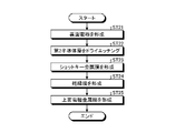
- FIG. 5 is a process diagram for explaining a method for manufacturing a semiconductor device according to an embodiment. The method for manufacturing the semiconductor element 1 is executed according to the process shown in FIG.
- the substrate 11 shown in FIGS. 1 and 2 is an n + type self-supporting GaN.
- the doping amount of the n-type impurity is controlled in the substrate 11 so that the electron carrier concentration is 10 18 cm -3 or more.
- the back surface 11b of the surface layer of the substrate 11 opposite to the front surface 11a of the GaN layer may be supported by other than GaN such as a silicon substrate (not shown).
- the substrate that supports the back surface 11b of the GaN layer on the surface of the substrate 11 may be, for example, a sapphire substrate or a SiC (Silicon Carbide) substrate.
- a mask 21 made of SiO 2 is formed on the surface 11a of the GaN layer on the surface of the substrate 11 shown in FIG. 2 (step ST11) (first step). More specifically, a mask 21 having an opening 22 is provided on the surface 11a of the substrate 11.
- the mask 21 may contain an element that becomes a donor in the semiconductor layer 31.
- metals such as W and Ti, nitrides such as SiN and AlN, and oxides such as Al 2 O 3 and Ga 2 O 3 may be used.
- the mask 21 may be amorphous.
- the mask 21 has an opening 22.
- the surface 11a of the substrate 11 in the portion corresponding to the opening 22 is exposed from the opening 22 of the mask 21.
- the surfaces 11a located at both ends of the substrate 11 may be covered with the mask 21. Further, the entire side surface or the back surface of the substrate 11 may be covered with the mask 21. Of the surfaces that can come into contact with the raw material gas used in the vapor phase growth method described later, the entire surface except the opening 22 may be covered with the mask 21.
- the width w1 in the lateral direction orthogonal to the stacking direction of the mask 21 is, for example, 10 ⁇ m or more.
- the thickness of the mask 21 in the stacking direction is, for example, 100 nm.
- a GaN layer as a semiconductor layer 31 is formed from the surface 11a of the substrate 11 exposed from the opening 22 by using the above-mentioned ELO technique (step ST12) (second step). More specifically, using ELO technology, in an epitaxial device (not shown), GaN is epitaxially grown from the surface 11a of the substrate 11 exposed from the opening 22 along the mask 21, and an n + type GaN layer 32 having a high impurity concentration is epitaxially grown. ..
- the GaN layer 32 grows vertically from the surface 11a exposed from the opening 22 above the stacking direction of the opening 22, and grows laterally on the outer peripheral side of the opening 22.
- the surface 32a of the GaN layer 32 is substantially flat.
- the GaN layer 32 is auto-doped with impurities from the material constituting the mask 21.
- the impurity is Si (Silicon)
- the GaN layer 32 is a highly concentrated n + semiconductor layer.
- the doping amount of n-type impurities is controlled so that the electron carrier concentration is 10 18 cm -3 or more.
- impurities for example, Si
- the thickness of the GaN layer 32 in the stacking direction is, for example, 10 ⁇ m or more.
- a GaN layer 33 having a low impurity concentration is formed so as to cover the GaN layer 32 (step ST13) (third step). More specifically, an n ⁇ type GaN layer 33 having a low impurity concentration is formed from the surface 32a of the GaN layer 32.
- the GaN layer 33 is grown by selecting from the surface 32a of the GaN layer 32 the conditions under which the growth in the vertical direction is superior to the growth in the horizontal direction.
- the surface 33a of the GaN layer 33 is substantially flat.
- the surface 33a of the GaN layer 33 is a surface located on the opposite side of the substrate 11 in the stacking direction and provided with a top electrode.
- the GaN layer 33 is an n-semiconductor layer.
- the doping amount of the n-type impurity is controlled in the GaN layer 33 so that the electron carrier concentration is less than 10 17 cm -3 . Since the GaN layer 33 does not come into contact with the mask 21 and is covered with the GaN layer 32 during epitaxial growth, auto-doping is reduced.
- the thickness of the GaN layer 33 in the stacking direction is, for example, 5 ⁇ m or more for a device having a withstand voltage of 600 V.
- a semiconductor is epitaxially grown from the surface 11a exposed from the opening 22 along the mask 21 to produce a semiconductor element 1 having a semiconductor layer 31.
- the semiconductor layer 31 is formed on the substrate 11, and the GaN layer 32, which is an n + type semiconductor layer, and the GaN layer 33, which is an n ⁇ type semiconductor layer, are epitaxially grown from the surface in the stacking direction.
- the semiconductor element 1 has a hexagonal shape when viewed from above in the stacking direction. This is because the growth direction of the crystal in epitaxial growth is fixed.
- the semiconductor layer 31 of the semiconductor element 1 crystals grow in the vertical direction above the stacking direction of the openings 22, and crystals grow in the horizontal direction on the outer peripheral side of the openings 22.
- the crystal defects on the surface 33a of the GaN layer 33 of the semiconductor element 1 extend in the vertical direction in the central portion and extend in the horizontal direction on the outer peripheral side from the central portion.
- FIG. 6 is a process diagram for explaining a method for manufacturing a semiconductor device according to an embodiment.
- the manufacturing method of the semiconductor device 2 is executed according to the process shown in FIG. 6 after the semiconductor element 1 is manufactured according to the process shown in FIG. Steps ST21 to ST22 are performed after performing steps ST11 to ST13.
- the back surface electrode 61 is formed on the back surface 11b opposite to the semiconductor layer 31 of the substrate 11 (step ST21). More specifically, the back surface electrode 61 is formed on the back surface 11b of the substrate 11 by, for example, sputtering.
- the back surface electrode 61 is, for example, an Al layer plated with Ti, Ni, or Au.
- the back surface electrode 61 may be formed after the Schottky electrode 41 described later is formed. When the step of raising the temperature is included, the influence on the back surface electrode 61 can be avoided by performing step ST21 at the end.
- a Schottky electrode 41 which is a metal layer (barrier metal), is formed on the surface 33a of the GaN layer 33 of the semiconductor layer 31 (step ST22). As a result, a Schottky junction between the GaN layer 33 and the Schottky electrode 41 is provided.
- the Schottky metal film 41 is, for example, Ni, Al, Pd, or the like.
- the Schottky metal film 41 is located on the opposite side of the substrate 11 in the stacking direction.
- the Schottky metal film 41 is provided at the center of the surface 33a of the GaN layer 33.
- the width (width of the end pressure resistant portion) w2 from the end of the surface 33a of the GaN layer 33 to the Schottky metal film 41 is smaller than the width w1 of the mask 21.
- the portion from the end portion of the surface 33a to the Schottky metal film 41 is referred to as an end pressure resistant portion.
- the semiconductor element 1 is manufactured.
- the manufactured semiconductor device 1 can be used, for example, as an SBD having a Schottky junction.
- a mask 21 is interposed between the substrate 11 and the GaN layer 32.
- the manufacturing process described above may be carried out simultaneously and simultaneously so as to manufacture a plurality of semiconductor elements 1 at the same time.
- a plurality of openings 22 are formed in a stripe shape on the mask 21.
- By associating one semiconductor element 1 with one opening 22, a plurality of semiconductor elements 1 can be manufactured at the same time.
- the crystal has a hexagonal shape with two long sides, and the cross-sectional view of the two long sides is as shown in FIG.
- Each semiconductor element 1 manufactured at the same time may be separated into individual pieces to form a semiconductor device 2.
- the substrate 11 and the back surface electrode 61 may be mounted as shown in FIG. 4 while being shared by the plurality of semiconductor elements 1 and used as the semiconductor device 2.
- a common back surface electrode 61 is die-bonded to one electrode pad 201 on the mounting substrate 200, and individual top electrode metal films (not shown) are bonded to another electrode pad by a bonding wire 52. Connect to 202.
- a plurality of diodes can be connected in parallel to increase the capacity and use them.
- the plurality of semiconductor elements 1 are manufactured so as to be arranged side by side in a certain direction.
- the semiconductor element 1 has a long shape in a direction substantially orthogonal to the direction in which the semiconductor elements 1 are arranged in a stacking direction. By arranging the semiconductor elements 1 in line with such a shape, the junction area of the diode can be increased.
- the semiconductor element 1 manufactured in this way can be used as various semiconductor devices 2 according to the application.
- the mask 21 is interposed between the substrate 11 and the GaN layer 32 inside the semiconductor element 1.
- the width w2 from the end of the surface 33a of the GaN layer 33 to the Schottky metal film 41 is smaller than the width w1 of the mask 21.
- the crystal grows in the vertical direction above the stacking direction of the opening 22, and the crystal grows in the horizontal direction on the outer peripheral side of the opening 22.
- the direction of the crystal defect in the end pressure resistant portion is the lateral direction.
- the width w1 of the mask 21 is, for example, 10 ⁇ m or more.
- the width w2 ( ⁇ w1) of the end pressure resistant portion can be narrowed.
- the ratio of the energized region of the semiconductor element 1 can be increased.
- the semiconductor element 1 can be miniaturized, so that the cost can be reduced.
- FIG. 7 is a schematic cross-sectional view for explaining an example of the semiconductor element according to the first modification of the embodiment.
- FIG. 8 is a process diagram for explaining a method for manufacturing a semiconductor device according to the first modification of the embodiment.
- the semiconductor element 1 according to the modified example 1 has a mesa structure and a field plate structure.
- the semiconductor device 2 includes such a semiconductor element 1.
- a large step is drawn for the sake of explanation. The same applies to the following figure.
- Steps ST11 and ST12 are performed in the same manner as in the embodiment.
- the semiconductor element 1 is manufactured in the same manner as in the embodiment.
- Step ST21 is performed in the same manner as in the embodiment. That is, after performing steps ST11 to ST21 of the embodiment, the steps of steps ST22 to ST25 are executed.
- a part of the GaN layer 33 is dry etched (step ST22). More specifically, a part of the surface 33a of the GaN layer 33 is dry-etched. Specifically, the outer peripheral portion of the GaN layer 33 is dry-etched. The end of the surface 33a of the GaN layer 33 has a mesa structure. In other words, the outer peripheral portion of the remaining GaN layer 33 has a mesa step 33s. The outer peripheral portion of the GaN layer 33 has the surface 33c at a position closer to the GaN layer 32 than the surface 33a, in other words, at a position one step lower.
- a Schottky metal film 41 to be Schottky bonded is formed on the surface 33a of the exposed GaN layer 33 (step ST23).
- the surface 33a of the exposed GaN layer 33 is covered with the Schottky metal film 41.
- a Schottky junction between the GaN layer 33 and the Schottky metal film 41 is provided.
- the insulating film 42 which is an insulating layer, is formed (step ST24).
- the insulating film 42 is arranged so as to cover the exposed GaN layer 33 and the outer peripheral portion of the Schottky metal film 41.
- the insulating film 42 has a wall portion 421 that covers the outer peripheral portion of the Schottky metal film 41, a wall portion 422 that covers the side surface 33b of the GaN layer 33, and a wall portion 423 that covers the surface 33c of the GaN layer 33.
- the wall portion 421 has an opening in the central portion that exposes the Schottky metal film 41.
- the wall portion 422 extends downward in the stacking direction from the end portion on the outer peripheral side of the wall portion 421.
- the wall portion 423 extends from the lower end portion of the wall portion 422 in the stacking direction toward the outer peripheral side.
- the top electrode metal film 43 is formed on the Schottky metal film 41 and the insulating film 42 (step ST25).
- the top electrode metal film 43 forms a so-called field plate on the insulating film 42.
- the outer peripheral end of the wall 423 of the insulating film 42 is exposed from the top electrode metal film 43.
- the back surface electrode forming step, step ST21, may be performed after step ST25 if the Schottky metal film 41, the insulating film 42, and the top surface electrode metal film 43 are not affected by the annealing temperature.
- the semiconductor element 1 having a mesa structure and a field plate structure is manufactured.
- the field plate By having the field plate, the electric field applied to the end of the top electrode can be relaxed, so that the device has a high withstand voltage.
- the field plate may be separated from the top electrode.
- the electric field applied to the end of the top electrode can be relaxed by having the mesa step 33s.
- the electric field applied to the end of the top electrode can be relaxed by having the field plate.
- the semiconductor element 1 having an increased surge withstand current can be manufactured.
- the semiconductor element 1 having improved withstand voltage can be manufactured.
- the crystal direction at the end withstand voltage portion is the lateral direction, and the occurrence of crystal defects on the surface along the electric field direction that can be the path of the leakage current of the semiconductor element 1 is reduced.
- the height of the mesa step 33s in the stacking direction can be lowered.
- the width w2 of the end pressure resistant portion can be narrowed.
- the ratio of the energized region of the semiconductor element 1 can be increased.
- the semiconductor element 1 can be miniaturized, so that the cost can be reduced.
- FIG. 9 is a schematic cross-sectional view for explaining the semiconductor device according to the second modification of the embodiment.
- the semiconductor element 1 according to the second modification has a mesa structure, a field plate structure, and a trench structure.
- Steps ST11 to ST13 are performed in the same manner as in the embodiment.
- the semiconductor element 1 is manufactured in the same manner as in the embodiment.
- Step ST21 is performed in the same manner as in the embodiment. That is, after performing steps ST11 to ST21 of the embodiment, the steps of steps ST22 to ST25 are executed.
- steps ST11 to ST21 of the embodiment the steps of steps ST22 to ST25 are executed.
- a process different from that of the first modification will be described.
- a mesa step 33s and a trench structure 33t are formed on the GaN layer 33 by dry etching. More specifically, the outer peripheral portion of the remaining GaN layer 33 has a mesa step 33s. A groove-shaped trench structure 33t is provided inside the outer peripheral portion of the remaining GaN layer 33. In the GaN layer 33, a part of the surface 33a remains in the portion where the mesa step 33s and the trench structure 33t are not formed.
- step ST23 the Schottky metal film 41 is formed on the surface 33a remaining inside the mesa step 33s.
- the insulating film 42 is formed by covering the exposed surface of the GaN layer 33, which is not covered by the Schottky metal film 41.
- step ST25 the top electrode metal film 43 is formed on the Schottky metal film 41 and the insulating film 42.
- the semiconductor element 1 having a mesa structure, a field plate structure, and a trench structure is manufactured.
- FIG. 10 is a schematic cross-sectional view for explaining the semiconductor device according to the third modification of the embodiment.
- the semiconductor element 1 according to the third modification has a mesa structure, a field plate structure, and a JBS structure.
- the semiconductor layer 31 of the semiconductor element 1 according to the third modification is the GaN layer (first semiconductor layer) 32 which is an n + type semiconductor layer and the GaN layer (second semiconductor layer) which is an n ⁇ type semiconductor layer in the order of proximity to the substrate 11. ) 33, and a GaN layer (first semiconductor layer) 34, which is a p + type semiconductor layer, are laminated.
- step ST14 (not shown) is executed.
- a p + type GaN layer 34 having a high impurity concentration is formed so as to cover the GaN layer 33 (step ST14).
- the doping amount of the p-type impurity is controlled in the GaN layer 34 so that the hole carrier concentration is 10 18 cm -3 or more.
- the surface of the GaN layer 34 is substantially flat.
- the thickness of the GaN layer 34 in the stacking direction is, for example, 20 nm or more.
- Steps ST21 and ST25 are performed in the same manner as in the second modification.
- step ST22 a part of the GaN layer 34 and the GaN layer 33 is dry-etched to form the mesa step 33s and the trench structure 33t.
- the Schottky metal film 41 is formed on the GaN layer 34 and the GaN layer 33 exposed inside the mesa step 33s and outside the GaN layer 34 and the GaN layer 33 left in the center. In other words, the Schottky metal film 41 is arranged except for the central portion and the end portion in the stacking direction view.
- the insulating film 42 is formed by covering the exposed surface of the GaN layer 33 that is not covered by the Schottky metal film 41.
- the semiconductor element 1 having a mesa structure, a field plate structure, and a JBS structure is manufactured.
- the semiconductor device 1 having a JBS structure is not limited to this.
- the semiconductor element 1 may be a Schottky barrier diode.
- the electric field applied to the central portion of the top electrode can be relaxed.
- the semiconductor element 1 having higher withstand voltage can be manufactured.
- the leakage current can be reduced.
Landscapes
- Electrodes Of Semiconductors (AREA)
Priority Applications (4)
| Application Number | Priority Date | Filing Date | Title |
|---|---|---|---|
| EP21906422.7A EP4266350A1 (en) | 2020-12-17 | 2021-12-06 | Method for manufacturing semiconductor element, semiconductor element, and semiconductor device |
| CN202180082891.8A CN116569338A (zh) | 2020-12-17 | 2021-12-06 | 半导体元件的制造方法、半导体元件以及半导体装置 |
| JP2022569881A JPWO2022131059A1 (https=) | 2020-12-17 | 2021-12-06 | |
| US18/333,747 US20230326993A1 (en) | 2020-12-17 | 2023-06-13 | Manufacturing method for semiconductor element, semiconductor element, and semiconductor device |
Applications Claiming Priority (2)
| Application Number | Priority Date | Filing Date | Title |
|---|---|---|---|
| JP2020209672 | 2020-12-17 | ||
| JP2020-209672 | 2020-12-17 |
Related Child Applications (1)
| Application Number | Title | Priority Date | Filing Date |
|---|---|---|---|
| US18/333,747 Continuation US20230326993A1 (en) | 2020-12-17 | 2023-06-13 | Manufacturing method for semiconductor element, semiconductor element, and semiconductor device |
Publications (1)
| Publication Number | Publication Date |
|---|---|
| WO2022131059A1 true WO2022131059A1 (ja) | 2022-06-23 |
Family
ID=82057670
Family Applications (1)
| Application Number | Title | Priority Date | Filing Date |
|---|---|---|---|
| PCT/JP2021/044789 Ceased WO2022131059A1 (ja) | 2020-12-17 | 2021-12-06 | 半導体素子の製造方法、半導体素子及び半導体装置 |
Country Status (5)
| Country | Link |
|---|---|
| US (1) | US20230326993A1 (https=) |
| EP (1) | EP4266350A1 (https=) |
| JP (1) | JPWO2022131059A1 (https=) |
| CN (1) | CN116569338A (https=) |
| WO (1) | WO2022131059A1 (https=) |
Citations (5)
| Publication number | Priority date | Publication date | Assignee | Title |
|---|---|---|---|---|
| JP2012124268A (ja) * | 2010-12-07 | 2012-06-28 | Nippon Inter Electronics Corp | 半導体装置 |
| JP2015056471A (ja) * | 2013-09-11 | 2015-03-23 | 株式会社東芝 | 半導体装置及びその製造方法 |
| JP2015099903A (ja) * | 2013-10-17 | 2015-05-28 | ローム株式会社 | 窒化物半導体装置およびその製造方法 |
| JP6070422B2 (ja) | 2013-05-31 | 2017-02-01 | 豊田合成株式会社 | 半導体素装置の製造方法及び半導体装置 |
| WO2019232230A1 (en) * | 2018-05-30 | 2019-12-05 | The Regents Of The University Of California | Method of removing semiconducting layers from a semiconducting substrate |
Family Cites Families (5)
| Publication number | Priority date | Publication date | Assignee | Title |
|---|---|---|---|---|
| JP4667556B2 (ja) * | 2000-02-18 | 2011-04-13 | 古河電気工業株式会社 | 縦型GaN系電界効果トランジスタ、バイポーラトランジスタと縦型GaN系電界効果トランジスタの製造方法 |
| JP2009076866A (ja) * | 2007-08-31 | 2009-04-09 | Sumitomo Electric Ind Ltd | ショットキーバリアダイオード |
| JP5681937B2 (ja) * | 2010-11-25 | 2015-03-11 | 株式会社パウデック | 半導体素子およびその製造方法 |
| JP5888214B2 (ja) * | 2012-11-30 | 2016-03-16 | 富士電機株式会社 | 窒化物系化合物半導体装置およびその製造方法 |
| JP2016031953A (ja) * | 2014-07-25 | 2016-03-07 | 株式会社タムラ製作所 | 半導体素子及びその製造方法、半導体基板、並びに結晶積層構造体 |
-
2021
- 2021-12-06 JP JP2022569881A patent/JPWO2022131059A1/ja active Pending
- 2021-12-06 EP EP21906422.7A patent/EP4266350A1/en not_active Withdrawn
- 2021-12-06 WO PCT/JP2021/044789 patent/WO2022131059A1/ja not_active Ceased
- 2021-12-06 CN CN202180082891.8A patent/CN116569338A/zh active Pending
-
2023
- 2023-06-13 US US18/333,747 patent/US20230326993A1/en active Pending
Patent Citations (5)
| Publication number | Priority date | Publication date | Assignee | Title |
|---|---|---|---|---|
| JP2012124268A (ja) * | 2010-12-07 | 2012-06-28 | Nippon Inter Electronics Corp | 半導体装置 |
| JP6070422B2 (ja) | 2013-05-31 | 2017-02-01 | 豊田合成株式会社 | 半導体素装置の製造方法及び半導体装置 |
| JP2015056471A (ja) * | 2013-09-11 | 2015-03-23 | 株式会社東芝 | 半導体装置及びその製造方法 |
| JP2015099903A (ja) * | 2013-10-17 | 2015-05-28 | ローム株式会社 | 窒化物半導体装置およびその製造方法 |
| WO2019232230A1 (en) * | 2018-05-30 | 2019-12-05 | The Regents Of The University Of California | Method of removing semiconducting layers from a semiconducting substrate |
Also Published As
| Publication number | Publication date |
|---|---|
| EP4266350A1 (en) | 2023-10-25 |
| CN116569338A (zh) | 2023-08-08 |
| JPWO2022131059A1 (https=) | 2022-06-23 |
| US20230326993A1 (en) | 2023-10-12 |
Similar Documents
| Publication | Publication Date | Title |
|---|---|---|
| US7679104B2 (en) | Vertical type semiconductor device and manufacturing method of the device | |
| US7745848B1 (en) | Gallium nitride material devices and thermal designs thereof | |
| US8026596B2 (en) | Thermal designs of packaged gallium nitride material devices and methods of packaging | |
| JP2007242853A (ja) | 半導体基体及びこれを使用した半導体装置 | |
| US9779988B2 (en) | Semiconductor devices with inner via | |
| JP2013080895A (ja) | 窒化物半導体素子及びその製造方法 | |
| TW201234538A (en) | Gallium nitride power devices using island topography | |
| TW200525783A (en) | Light-emitting semiconductor device and method of fabrication | |
| JP4210823B2 (ja) | シヨットキバリアダイオード及びその製造方法 | |
| KR20110123118A (ko) | 패터닝된 발광부를 구비한 수직형 발광소자 | |
| US12107157B2 (en) | High electron mobility transistor and method for fabricating the same | |
| JP6428900B1 (ja) | ダイオード素子およびダイオード素子の製造方法 | |
| JP4058595B2 (ja) | 半導体発光素子及びその製造方法 | |
| US20150325689A1 (en) | Iii-v transistor and method for manufacturing same | |
| JP5362187B2 (ja) | 半導体素子 | |
| KR20130082307A (ko) | 기판 구조체, 이로부터 제조된 반도체소자 및 그 제조방법 | |
| WO2022131059A1 (ja) | 半導体素子の製造方法、半導体素子及び半導体装置 | |
| KR102937797B1 (ko) | 질화 갈륨 파워 디바이스 | |
| JP2009194225A (ja) | ショットキバリアダイオード、及びショットキバリアダイオードを作製する方法 | |
| JP4058592B2 (ja) | 半導体発光素子及びその製造方法 | |
| JP2008159842A (ja) | 半導体装置及びその製造方法 | |
| JP4058593B2 (ja) | 半導体発光素子 | |
| WO2022025080A1 (ja) | 半導体素子の製造方法、半導体素子及び半導体装置 | |
| JP4041906B2 (ja) | 半導体発光素子 | |
| JP4058594B2 (ja) | 半導体発光素子 |
Legal Events
| Date | Code | Title | Description |
|---|---|---|---|
| 121 | Ep: the epo has been informed by wipo that ep was designated in this application |
Ref document number: 21906422 Country of ref document: EP Kind code of ref document: A1 |
|
| ENP | Entry into the national phase |
Ref document number: 2022569881 Country of ref document: JP Kind code of ref document: A |
|
| WWE | Wipo information: entry into national phase |
Ref document number: 202180082891.8 Country of ref document: CN |
|
| NENP | Non-entry into the national phase |
Ref country code: DE |
|
| ENP | Entry into the national phase |
Ref document number: 2021906422 Country of ref document: EP Effective date: 20230717 |