WO2022124395A1 - 電力変換装置 - Google Patents
電力変換装置 Download PDFInfo
- Publication number
- WO2022124395A1 WO2022124395A1 PCT/JP2021/045518 JP2021045518W WO2022124395A1 WO 2022124395 A1 WO2022124395 A1 WO 2022124395A1 JP 2021045518 W JP2021045518 W JP 2021045518W WO 2022124395 A1 WO2022124395 A1 WO 2022124395A1
- Authority
- WO
- WIPO (PCT)
- Prior art keywords
- power conversion
- circuit
- inductor
- voltage
- current
- Prior art date
- Legal status (The legal status is an assumption and is not a legal conclusion. Google has not performed a legal analysis and makes no representation as to the accuracy of the status listed.)
- Ceased
Links
Images


Classifications
-
- H—ELECTRICITY
- H02—GENERATION; CONVERSION OR DISTRIBUTION OF ELECTRIC POWER
- H02M—APPARATUS FOR CONVERSION BETWEEN AC AND AC, BETWEEN AC AND DC, OR BETWEEN DC AND DC, AND FOR USE WITH MAINS OR SIMILAR POWER SUPPLY SYSTEMS; CONVERSION OF DC OR AC INPUT POWER INTO SURGE OUTPUT POWER; CONTROL OR REGULATION THEREOF
- H02M1/00—Details of apparatus for conversion
- H02M1/14—Arrangements for reducing ripples from DC input or output
- H02M1/15—Arrangements for reducing ripples from DC input or output using active elements
-
- H—ELECTRICITY
- H02—GENERATION; CONVERSION OR DISTRIBUTION OF ELECTRIC POWER
- H02M—APPARATUS FOR CONVERSION BETWEEN AC AND AC, BETWEEN AC AND DC, OR BETWEEN DC AND DC, AND FOR USE WITH MAINS OR SIMILAR POWER SUPPLY SYSTEMS; CONVERSION OF DC OR AC INPUT POWER INTO SURGE OUTPUT POWER; CONTROL OR REGULATION THEREOF
- H02M3/00—Conversion of DC power input into DC power output
- H02M3/02—Conversion of DC power input into DC power output without intermediate conversion into AC
- H02M3/04—Conversion of DC power input into DC power output without intermediate conversion into AC by static converters
- H02M3/10—Conversion of DC power input into DC power output without intermediate conversion into AC by static converters using discharge tubes with control electrode or semiconductor devices with control electrode
- H02M3/145—Conversion of DC power input into DC power output without intermediate conversion into AC by static converters using discharge tubes with control electrode or semiconductor devices with control electrode using devices of a triode or transistor type requiring continuous application of a control signal
- H02M3/155—Conversion of DC power input into DC power output without intermediate conversion into AC by static converters using discharge tubes with control electrode or semiconductor devices with control electrode using devices of a triode or transistor type requiring continuous application of a control signal using semiconductor devices only
- H02M3/156—Conversion of DC power input into DC power output without intermediate conversion into AC by static converters using discharge tubes with control electrode or semiconductor devices with control electrode using devices of a triode or transistor type requiring continuous application of a control signal using semiconductor devices only with automatic control of output voltage or current, e.g. switching regulators
- H02M3/158—Conversion of DC power input into DC power output without intermediate conversion into AC by static converters using discharge tubes with control electrode or semiconductor devices with control electrode using devices of a triode or transistor type requiring continuous application of a control signal using semiconductor devices only with automatic control of output voltage or current, e.g. switching regulators including plural semiconductor devices as final control devices for a single load
-
- H—ELECTRICITY
- H02—GENERATION; CONVERSION OR DISTRIBUTION OF ELECTRIC POWER
- H02M—APPARATUS FOR CONVERSION BETWEEN AC AND AC, BETWEEN AC AND DC, OR BETWEEN DC AND DC, AND FOR USE WITH MAINS OR SIMILAR POWER SUPPLY SYSTEMS; CONVERSION OF DC OR AC INPUT POWER INTO SURGE OUTPUT POWER; CONTROL OR REGULATION THEREOF
- H02M1/00—Details of apparatus for conversion
- H02M1/14—Arrangements for reducing ripples from DC input or output
- H02M1/143—Arrangements for reducing ripples from DC input or output using compensating arrangements
-
- H—ELECTRICITY
- H02—GENERATION; CONVERSION OR DISTRIBUTION OF ELECTRIC POWER
- H02M—APPARATUS FOR CONVERSION BETWEEN AC AND AC, BETWEEN AC AND DC, OR BETWEEN DC AND DC, AND FOR USE WITH MAINS OR SIMILAR POWER SUPPLY SYSTEMS; CONVERSION OF DC OR AC INPUT POWER INTO SURGE OUTPUT POWER; CONTROL OR REGULATION THEREOF
- H02M3/00—Conversion of DC power input into DC power output
- H02M3/02—Conversion of DC power input into DC power output without intermediate conversion into AC
- H02M3/04—Conversion of DC power input into DC power output without intermediate conversion into AC by static converters
- H02M3/10—Conversion of DC power input into DC power output without intermediate conversion into AC by static converters using discharge tubes with control electrode or semiconductor devices with control electrode
- H02M3/145—Conversion of DC power input into DC power output without intermediate conversion into AC by static converters using discharge tubes with control electrode or semiconductor devices with control electrode using devices of a triode or transistor type requiring continuous application of a control signal
- H02M3/155—Conversion of DC power input into DC power output without intermediate conversion into AC by static converters using discharge tubes with control electrode or semiconductor devices with control electrode using devices of a triode or transistor type requiring continuous application of a control signal using semiconductor devices only
- H02M3/156—Conversion of DC power input into DC power output without intermediate conversion into AC by static converters using discharge tubes with control electrode or semiconductor devices with control electrode using devices of a triode or transistor type requiring continuous application of a control signal using semiconductor devices only with automatic control of output voltage or current, e.g. switching regulators
- H02M3/158—Conversion of DC power input into DC power output without intermediate conversion into AC by static converters using discharge tubes with control electrode or semiconductor devices with control electrode using devices of a triode or transistor type requiring continuous application of a control signal using semiconductor devices only with automatic control of output voltage or current, e.g. switching regulators including plural semiconductor devices as final control devices for a single load
- H02M3/1584—Conversion of DC power input into DC power output without intermediate conversion into AC by static converters using discharge tubes with control electrode or semiconductor devices with control electrode using devices of a triode or transistor type requiring continuous application of a control signal using semiconductor devices only with automatic control of output voltage or current, e.g. switching regulators including plural semiconductor devices as final control devices for a single load with a plurality of power processing stages connected in parallel
- H02M3/1586—Conversion of DC power input into DC power output without intermediate conversion into AC by static converters using discharge tubes with control electrode or semiconductor devices with control electrode using devices of a triode or transistor type requiring continuous application of a control signal using semiconductor devices only with automatic control of output voltage or current, e.g. switching regulators including plural semiconductor devices as final control devices for a single load with a plurality of power processing stages connected in parallel switched with a phase shift, i.e. interleaved
Definitions
- the present disclosure relates to a power conversion device such as a switching power supply circuit.
- a triangular wave-shaped ripple current is generated by repeatedly accumulating and releasing magnetic (current) energy in the reactor. If this ripple current propagates outside the switching power supply circuit, there is a concern that it will adversely affect other electronic devices as electromagnetic noise. Therefore, it is necessary to suppress the propagation of the ripple current inside the switching power supply circuit.
- Patent Document 1 discloses a method for suppressing a ripple current by an interleave method.
- two-phase interleaving it is possible to suppress odd-order harmonic components among the frequency components included in the triangular wave-shaped ripple current.
- the even-order harmonic component increases by 6 dB (twice).
- Patent Document 2 discloses a suppression method by a frequency diffusion control method. It fluctuates the switching frequency and prevents the noise energy from concentrating on a single frequency.
- the switching frequency is varied from 90 kHz to 110 kHz
- the energy of the fundamental wave is dispersed in the range of 90 kHz to 110 kHz (range of 20 kHz)
- the energy of the second harmonic is distributed in the range of 180 kHz to 220 kHz (range of 40 kHz). That is, in the high-order harmonics, the range of dispersion is wide and a large suppression effect can be obtained.
- the suppression effect is limited for fundamental waves and low-order harmonics. Further, when the peak value detection is used as the noise observation method, the noise suppression effect cannot be obtained.
- Patent Document 3 discloses a suppression method using a bypass circuit. By magnetically coupling the inductor of the bypass circuit and the reactor, the fundamental wave component of the ripple current can be significantly suppressed. On the other hand, the suppression effect on harmonic components is low.
- An object of the present disclosure is to solve the above problems and to provide a power conversion device capable of suppressing all frequency components of a ripple current without using a large noise filter in a power conversion device which is a switching power supply circuit such as a boost converter. There is something in it.
- the power conversion device is A power conversion device having a pair of input terminals and a pair of output terminals. Using the second switch element, the first series circuit of the first inductor and the first switch element connected in parallel to the pair of input terminals and the voltage across the first switch element are used.
- a power conversion including a power conversion circuit including a switching circuit for switching and outputting, converting an input voltage input to the pair of input terminals to a predetermined output voltage, and then outputting the power to the pair of output terminals. It ’s a device, The power conversion device generates a ripple canceling current that cancels the ripple current generated by the accumulation and emission of current energy in the first inductor when the first switch element is controlled to be turned on / off.
- a ripple canceling current generation circuit that cancels the ripple current by inputting to a pair of input terminals of the power conversion device.
- the ripple canceling current generation circuit is A second inductor having one end connected to one of the pair of input terminals, A second series circuit connected between the other end of the second inductor and the other of the pair of input terminals, in which the third switch element and the first capacitor are connected in series.
- the first series circuit configured in A third series circuit connected in parallel to the first series circuit, the third series circuit configured by connecting the fourth switch element and the second capacitor in series.
- a power supply device that applies a predetermined applied voltage to the second capacitor, and To prepare for.
- the triangular wave-shaped ripple current can be canceled out. That is, all frequency components of the ripple current can be suppressed. As a result, it is possible to reduce the noise filter, reduce the size and weight of the device, and reduce the cost as compared with the conventional power conversion device.
- FIG. It is a block diagram which shows the structural example of the power conversion apparatus which concerns on Embodiment 1.
- FIG. It is a block diagram which shows the structural example of the control circuit 10 of FIG. 1A. It is a timing chart which shows the current I1 flowing through the inductor L1 with respect to the gate control signal G1 of FIG. 1A.
- FIG. 3 is a timing chart showing the relationship between the gate control signals G1 to G4 of FIG. 1A and the current waveforms of the currents I1 and I2 of the inductors L1 and L2.
- FIG. 3 is a circuit diagram showing a configuration example of a switching circuit 11-2 according to a second embodiment applied to the power conversion device of FIG. 1A. It is a block diagram which shows the structural example of the power conversion apparatus which concerns on Embodiment 2. 8 is a timing chart showing the relationship between the gate control signals G1 to G6 of FIG.
- 12 is a timing chart showing the relationship between the gate control signals G7 to G10 of FIG. 12 and the currents I6 and I7 and the currents I6 + I7 of the inductors L6 and L7.
- It is a block diagram which shows the structural example of the power conversion apparatus which concerns on Embodiment 4.
- It is a block diagram which shows the structural example of the power conversion apparatus which concerns on Embodiment 5.
- It is a block diagram which shows the structural example of the control circuit 15 of FIG.
- FIG. 1A is a block diagram showing a configuration example of the power conversion device according to the first embodiment.
- the power conversion device of FIG. 1A includes an inductor L1 and a switching circuit 11, and after converting the voltage input to the pair of input terminals T1 and T2 into power such as DC / DC conversion, the pair of output terminals.
- a power conversion device including, for example, a DC / DC converter including a power conversion circuit 1 that outputs to T3 and T4, and an inductor L1 according to gate control signals G1 and G4 supplied from the control circuit 10 to the switching circuit 11.
- a ripple canceling current generation circuit that cancels the ripple current by generating a ripple canceling current that cancels the ripple current generated by the accumulation and release of the current energy to the input terminals T1 and T2 of the power conversion device. It is characterized by further providing 4.
- the power conversion circuit 1 has a pair of input terminals T1 and T2 and a pair of output terminals T3 and T4, and includes a smoothing circuit 5, a switch element S1, and a switching circuit 11. Will be done.
- the switching circuit 11 is, for example, a switching circuit 11-1 which is a step-up DC / DC converter of FIG. 11-2.
- the smoothing circuit 5 includes a smoothing capacitor C1 and an inductor L1 which is a reactor.
- the smoothing capacitor C1 is connected in parallel with the input terminals T1 and T2, and the inductor L1 is connected between the input terminal T1 and the input terminal T11 of the switching circuit 11.
- the switch element S1 is connected in parallel with the input terminals T11 and T12 of the switching circuit 11, and is controlled on / off according to the gate control signal G1 from the control circuit 10.
- the input terminal T2 is connected to the input terminal T12 of the switching circuit 11.
- the switching circuit 11 has input terminals T11 and T12 and output terminals T13 and T14, and after switching the voltage input to the input terminals T11 and T12 according to the gate control signal G4 from the control circuit 10, the output terminals T13, Output to output terminals T3 and T4 via T14.
- the ripple canceling current generation circuit 4 is connected in parallel with the input terminals T1 and T2 of the power conversion circuit 1, and is connected to a power supply device 12 that generates a predetermined applied voltage V1, an inductor L2, a switch element S2, S3, and a capacitor C2. It is configured with C3.
- the input terminal T1 is connected to the input terminal T2 via the inductor L2 and the series circuit of the switch element S2 and the capacitor C2, and is input via the inductor L2 and the series circuit of the switch element S3 and the capacitor C3. It is connected to the terminal T2.
- the power supply device 12 generates an applied voltage V1 and applies it to the connection point between the switch element S3 and the capacitor C3.
- the switch elements S2 and S3 are on / off controlled according to the gate control signals G2 and G3 from the control circuit 10, respectively.
- switch elements S1 to S4 are composed of, for example, MOS field effect transistors, and gate control signals G1 to G4 are applied to the gate from the control circuit 10. It is controlled on / off.
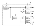
- FIG. 1B is a block diagram showing a configuration example of the control circuit 10 of FIG. 1A.
- the control circuit 10 includes a PWM signal generator 31, a delay circuit 32, inverters 33 and 34, and gate drivers 41 to 44.
- gate control signals G1 to G4 for driving the switch elements S1 to S4 are generated by the same control circuit 10, and the switch element S1 of the power conversion circuit 1 and the switch element S4 of the switching circuit 11 (described later). , Is transmitted to the switch elements S2 and S3. As a result, it is possible to prevent the switching timing from being deviated between the power conversion circuit 1 and the switch elements S2 and S3. If the switching timing is deviated, the ripple current suppression effect may be weakened. Therefore, the power conversion device of FIG. 1A can compensate for the ripple current suppression effect.
- the gate control signals G1 and G4 and the gate control signals G2 are corrected by, for example, the delay circuit 32 so as to correct the difference in the switching speed (transition time) between the switch element S1 and the switch elements S2 and S3.
- a delay may be added to any of G3.
- FIG. 1B after the PWM signal generator 31 generates a predetermined PWM signal, (1) A gate control signal G1 is generated via the gate driver 41. (2) A gate control signal G4 is generated via the inverter 33 and the gate driver 44. (3) A gate control signal G2 is generated via the delay circuit 32, the inverter 34, and the gate driver 42. (4) The gate control signal G3 is generated via the delay circuit 32 and the gate driver 43.
- the switch elements S2 and S3 use parts having a smaller rated current than the switch element S1. Since the switching speed tends to be faster for parts with a smaller rated current, it is possible to prevent the suppression effect from being weakened due to the difference.
- FIG. 2 is a timing chart showing the current I1 flowing through the inductor L1 with respect to the gate control signal G1 of FIG. 1A.
- the switch element applied to the gate is turned on, while when each gate control signal is at a low level, the switch applied to the gate is turned on. The element is turned off.
- the voltage Vin is input between the input terminals T1 and T2.
- the switch element S1 When the switch element S1 is on, magnetic energy is stored in the inductor L1.
- the switch element S1 when the switch element S1 is off, the magnetic energy of the inductor L1 is released.
- the current flowing through the inductor L1 becomes the sum of the DC amplitude Adc and the triangular wave amplitude Atri as shown in FIG.
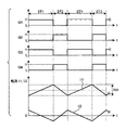
- FIG. 3 is a timing chart showing the relationship between the gate control signals G1 to G4 of FIG. 1A and the current waveforms of the currents I1 and I2 of the inductors L1 and L2.
- the switch element S1 when the switch element S1 is on, the switch element S2 is turned off and the switch element S3 is turned on (state ST1). Further, when the switch element S1 is off, the switch element S2 is turned on and the switch element S3 is turned off (state ST2). That is, the gate control signals G2 and G3 for the ripple canceling current generation circuit 4 are generated in synchronization with the gate control signals G1 and G4 of the power conversion circuit 1.
- the net current generated in the power conversion circuit 1 is the sum of the currents flowing through the inductor L1 and the inductor L2. That is, the triangular wave component of the current I1 flowing through the inductor L1 is canceled by the current I2 (ripple canceling current) flowing through the inductor L2.
- FIG. 4 is a block diagram showing a configuration example of a power conversion device according to the prior art.
- a noise filter 2 having input terminals T5 and T6 is used in order to suppress the propagation of the ripple current Ips to the power supply.
- the noise filter 2 can be reduced.
- the noise filter 2 Since the noise filter 2 is connected in series with the power conversion circuit 1, a large current flows. Therefore, it is necessary to use a component having a large rated current, which causes an increase in size and cost.
- a component having a large rated current which causes an increase in size and cost.
- FIG. 3 only a small current corresponding to the triangular wave amplitude Atri flows through the inductor L2 and the switch elements S2 and S3 used in the first embodiment (the DC component does not flow). Therefore, parts with a small rated current can be used. This means not only small size and low cost mounting, but also low power loss in these components.
- the ripple canceling current generation circuit 4 since the ripple canceling current generation circuit 4 is connected in parallel with the power conversion circuit 1, it does not affect the basic operation of the power conversion circuit 1. That is, after the power conversion circuit 1 is optimally designed from the viewpoint of power conversion efficiency and the like, the design for reducing the ripple current can be carried out. Also, it is fundamentally different from the approach of "detecting" noise and trying to cancel it, and the ripple current can be canceled by simply driving it synchronously. This means that the suppression effect can be obtained even when there is disturbance noise that can cause a detection error, and it can be applied to devices with strong safety requirements such as in-vehicle devices.
- FIG. 5 is a circuit diagram showing a configuration example of the switching circuit 11-1 according to the first embodiment applied to the power conversion device of FIG. 1A.
- the switching circuit 11-1 includes a switch element S4 and a capacitor C4.
- the input terminal T11 is connected to the output terminal T13 via the switch element S4, and the input terminal T12 is connected to the output terminal T14.
- the capacitor C4 is connected in parallel with the output terminals T13 and T14.
- the power conversion circuit 1 when the switch elements S1 and S4 are alternately turned on / off, the power conversion circuit 1 operates as a step-up DC / DC converter.
- the power conversion circuit 1 is driven in the period T, where the duty ratio of the gate control signal G1 to the switch element S1 is D and the duty ratio of the gate control signal G4 to the switch element S4 is 1-D, FIG.
- the triangular wave amplitude Atri shown in is expressed by the following equation.
- Atri DT ⁇ (V1-Vin) / (a ⁇ L1) (2)
- the value of the applied voltage V1 of the power supply device 12 is set between (1 + 0.5a) ⁇ Vin and (1 + 1.5a) ⁇ Vin, a noise reduction effect of 6 dB or more can be obtained. .. That is, the amplitude of the noise current is suppressed to less than half. Also in this case, by reducing the number of parts of the noise filter 2, it is possible to realize miniaturization and cost reduction.
- FIG. 6 is a diagram showing simulation results in a power conversion device using the switching circuit 11-1 of FIG. 5, and is a timing chart showing currents I1 and I2 of inductors L1 and L2 and power supply inflow current Ips.
- the triangular wave component included in the current of the inductor L1 is canceled by the current I2 of the inductor L2.
- the power supply inflow current Ips propagating from the input terminal T1 to the power supply does not include the ripple component.
- switch elements S1 to S4 for example, a MOS field effect transistor or a transistor such as a GaN-HEMT (High Electron Mobility Transistor) may be used as the switch elements S1 to S4. Further, a diode may be used for the switch element S4, in which case the gate control signal G4 becomes unnecessary.
- MOS field effect transistor or a transistor such as a GaN-HEMT (High Electron Mobility Transistor) may be used as the switch elements S1 to S4.
- a diode may be used for the switch element S4, in which case the gate control signal G4 becomes unnecessary.
- a full bridge type diode rectifier circuit may be connected in front of the input terminals T1 and T2 to form a power factor improving circuit.
- an AC voltage is input to the input terminal of the power factor improving circuit, and the input voltage Vin to the power conversion circuit 1 fluctuates. Therefore, the applied voltage V1 of the power supply device 12 may be fluctuated accordingly.
- the noise filter 2 the effect of improving the power factor can also be obtained.
- FIG. 7 is a circuit diagram showing a configuration example of the switching circuit 11-2 according to the second embodiment applied to the power conversion device of FIG. 1A.
- the switching circuit 11-2 includes a switch element S4, capacitors C4 and C5, and an inductor L4.
- the input terminal T11 is connected to the output terminal T13 via the capacitor C5 and the switch element S4, and the input terminal T12 is connected to the output terminal T14.
- the capacitor C4 is connected in parallel with the output terminals T13 and T14.
- the inductor L4 is connected between the connection point of the capacitor C5 and the switch element S4 and the input terminal T12.
- the power conversion circuit 1 when the switch elements S1 and S4 are alternately turned on / off, the power conversion circuit 1 operates as a STEPIC (Single Ended Primery indicator Converter; elevating DC / DC converter).
- STEPIC Single Ended Primery indicator Converter; elevating DC / DC converter.
- the ripple current Ips can be offset in the same manner as in the case of the step-up DC / DC converter according to the first embodiment of the first embodiment.
- FIG. 8 is a block diagram showing a configuration example of the power conversion device according to the second embodiment.
- the power conversion device according to the second embodiment has the following differences as compared with the power conversion device according to the first embodiment of FIG. (1) Instead of the power conversion circuit 1, a power conversion circuit 1A is provided. (2) Instead of the smoothing circuit 5, a smoothing circuit 5A is provided. The smoothing circuit 5A further includes an inductor L5 which is a reactor in the smoothing circuit 5. (3) Compared to the power conversion circuit 1, the power conversion circuit 1A further includes a switch element S5 that is on / off controlled by the gate control signal G5.
- the input terminal T15 is further provided, and the switching circuit 11A which is turned on / off by the gate control signals G4 and G6 is provided.
- a control circuit 10A is provided in place of the control circuit 10. The control circuit 10A generates gate control signals G1 to G6. The difference will be described below.
- the input terminal T1 is connected to the input terminal T15 of the switching circuit 11A via the inductor L5 which is a reactor, and the input terminal T15 is connected to the input terminal T12 via the switch element S5.
- the power conversion circuit 1A constitutes a two-phase interleave circuit that drives the switch elements S1 and S5 with a shift of half a cycle (T / 2).
- FIG. 9 is a timing chart showing the relationship between the gate control signals G1 to G6 of FIG. 8 and the current waveforms of the currents I1, I2, I5 and the currents I1 + I5 of the inductors L1, L2, L5.
- FIG. 9 shows a current waveform when the duty ratio of the gate control signals G1 and G5 with respect to the switch elements S1 and S5 is larger than 0.5.
- the input current of the power conversion circuit 1A is the sum of the currents flowing through the inductors L1 and L5 (I1 + I5). That is, the gate control signals G2 and G3 for the ripple canceling current generation circuit 4 are generated in synchronization with the gate control signals G1 and G4 to G6 of the power conversion circuit 1.
- the switch element S2 is turned on and the switch element S3 is turned off in the state ST3. Further, in the state ST4, the switch element S2 is turned off and the switch element S3 is turned on.
- the current I2 of the inductor L2 increases in the state ST3 and the inductor in the state ST4, as shown in FIG. The current I2 of L2 decreases.
- the net current generated by the power converter in FIG. 8 is the sum of the currents flowing through the inductors L1, L5, and L2 (I1 + I2 + I5). That is, the triangular wave component included in the sum of the currents (I1 + I5) flowing through the inductors L1 and L5 is canceled by the current I2 flowing through the inductor L2. As a result, the noise filter 2 can be reduced as in the first embodiment.
- FIG. 10 is a circuit diagram showing a configuration example of the switching circuit 11A of FIG. 8 constituting the interleaved step-up DC / DC converter.
- the switching circuit 11A of FIG. 10 has the following differences as compared with the switching circuit 11-1 of FIG. (1) An input terminal T15 and a switch element S6 are further provided. (2) The input terminal T15 is connected to the output terminal T13 via a switch element S6 that is on / off controlled by the gate control signal G6.
- the switch elements S1 and S4 are alternately turned on / off, and the switch elements S5 and S6 are alternately turned on / off.
- the power conversion circuit 1A operates as an interleaved boost DC / DC converter.
- the duty ratio of the gate control signals G1 and G5 to the switch elements S1 and S5 is set to D
- the duty ratio of the gate control signals G4 and G6 to the switch elements S4 and S6 is set to 1-D
- the power conversion circuit 1A is driven in the period T.
- the triangular wave amplitude Atri shown in FIG. 9 is expressed by the following equation.
- Atri (2D-1) T ⁇ (Vin / L1) (4)
- the conditions under which the triangular wave component included in the sum of the currents flowing through the inductors L1 and L5 can be completely canceled are shown below.
- the sum of the currents flowing through the inductors L1 and L5 (I1 + I5) and the triangular wave amplitude Atri of the current I2 flowing through L2 need to match.
- the triangular wave amplitude Atri of the inductor L2 is expressed by the following equation.
- Atri (D-0.5) T ⁇ (V1-Vin) / (a ⁇ L1) (5)
- the value of the applied voltage V1 of the power supply device 12 is set to a value between (1 + a) ⁇ Vin and (1 + 3a) ⁇ Vin, a noise reduction effect of 6 dB or more can be obtained, that is, , The amplitude of the noise current is suppressed to less than half. Also in this case, by reducing the number of parts of the noise filter 2, it is possible to realize miniaturization and cost reduction.
- FIG. 11 is a diagram showing simulation results of the power conversion device of FIG. 8, and is a timing chart showing current waveforms of the currents I1, I2, I5, the currents I1 + I5, and the power supply inflow current Ips of the inductors L1, L2, and L5. ..
- FIG. 11 shows the effect of reducing the ripple current by the circuit simulation.
- the input voltage Vin 100V
- the current I1 of the inductor L1 and the current I5 of the inductor L5 contain a triangular wave component of 100 kHz, and are deviated from each other by half a cycle of 5 ⁇ s. Therefore, the sum of the currents (I1 + I5) of the inductors L1 and L5 includes a triangular wave component having a double frequency of 200 kHz. This is offset by the current I2 of the inductor L2. As a result, it can be confirmed that the current Ips propagating from the input terminal T1 to the power supply does not include the ripple component of the triangular wave.
- the inductors L1 and L5 may be magnetically coupled to each other.
- the inductors L1 and L5 can be mounted as one coupled inductor.
- the power conversion circuit 1 may be configured as an interleaved circuit having three or more phases.
- the control of the switch elements S2 and S3 and the applied voltage V1 of the power supply device 12 may be switched according to the operation method. That is, it may be operated according to the second embodiment during the interleave operation, and may be operated according to the first embodiment during the single-phase operation. As a result, noise can be suppressed regardless of the operation method of the interleave circuit.
- FIG. 12 is a block diagram showing a configuration example of the power conversion device according to the third embodiment.
- the power conversion device according to the third embodiment has the following differences as compared with the power conversion device according to the first embodiment of FIG. (1)
- a ripple canceling current generation circuit 4A is provided instead of the ripple canceling current generation circuit 4A.
- the ripple canceling current generation circuit 4A includes a voltage conversion circuit 3 instead of the power supply device 12.
- the voltage conversion circuit 3 is an example of a power supply device.
- a control circuit 10B is provided in place of the control circuit 10.
- the control circuit 10B generates gate control signals G1 to G4 and G7 to G10. The difference will be described below.
- FIG. 13 is a circuit diagram showing a configuration example of the voltage conversion circuit 3 of FIG.
- the voltage conversion circuit 3 includes capacitors C6 and C7, inductors L6 and L7, and switch elements S7 to S10.
- the switch elements S7 to S10 are on / off controlled by the gate control signals G7 to G10 from the control circuit 10B, respectively.
- the capacitor C6 is connected in parallel between the input terminal T21 and the input terminal T22, and the capacitor C7 is connected in parallel between the output terminals T23 and T24.
- the input terminal T21 is connected to the input terminal T22 and the output terminal T24 via the inductor L6 and the switch element S7, and is connected to the output terminal T23 via the inductor L6 and the switch element S9. Further, the input terminal T21 is connected to the output terminal T24 via the inductor L7 and the switch element S8, and is also connected to the output terminal T23 via the inductor L7 and the switch element S10.
- FIG. 14A is a timing chart showing the relationship between the gate control signals G1 to G4 of FIG. 12 and the currents I1 and I2 of the inductors L1 and L2.
- 14B is a timing chart showing the relationship between the gate control signals G7 to G10 of FIG. 12 and the currents I6, I7 and the currents I6 + I7 of the inductors L6 and L7.
- the gate control signal G7 for the switch elements S7 and S8 , G8 has a duty ratio of 0.5, and the switch elements S7 and S8 may be driven.
- the duty ratio is 0.5
- the triangular wave current flowing through the inductors L6 and L7 does not include even-order harmonic components. Therefore, when the switch elements S7 and S8 are driven by shifting them by half a cycle (interleave operation), the odd-order components are also canceled and no ripple is generated in the input current from the voltage conversion circuit 3.
- the ripple component of the input current of the power conversion circuit 1 is canceled by the triangular wave current of the inductor L2, and the voltage conversion circuit 3 does not generate the ripple current, so that the ripple current does not propagate to the terminals T1 and T2.
- the cancellation of the triangular wave currents of the inductors L1 and L2 is completed by the operation of the switch elements S1 to S4.
- the cancellation of the triangular wave currents of the inductors L6 and L7 is completed by the operation of the switch elements S7 to S10.
- the gate control signals G1 to G4 in FIG. 14A and the gate control signals G7 to G10 in FIG. 14B including the drive frequency and timing, and the gate control signals G1 to G10 can be operated asynchronously.
- the gate control signals G2 and G3 for the ripple canceling current generation circuit 4A are generated in synchronization with the gate control signals G1 and G4 of the power conversion circuit 1.
- a dedicated noise filter may be provided in front of the input terminals T21 and T22 of the voltage conversion circuit 3 to suppress the noise generated by the voltage conversion circuit 3. Since a large current does not flow in the voltage conversion circuit 3, a noise filter can be mounted in a small size and at low cost. For the same reason, the voltage conversion circuit 3 itself can be mounted in a small size and at low cost.
- FIG. 15 is a block diagram showing a configuration example of the power conversion device according to the fourth embodiment.
- the power conversion device according to the fourth embodiment has the following differences as compared with the power conversion device according to the first embodiment of FIG. (1)
- a ripple canceling current generation circuit 4B is provided instead of the ripple canceling current generation circuit 4B.
- the ripple canceling current generation circuit 4B includes a voltage conversion circuit 3A instead of the power supply device 12.
- the voltage conversion circuit 3A is an example of a power supply device. The difference will be described below.
- the voltage conversion circuit 3A converts the output voltage Vout of the power conversion circuit 1 into the applied voltage V1 and applies it to the capacitor C3.
- the feature of this embodiment is that the voltage conversion circuit 3A is not directly connected to the input terminals T1 and T2, so that the ripple current generated by the voltage conversion circuit 3A does not propagate to the input terminals T1 and T2. That is, the applied voltage V1 can be easily generated from the viewpoint of noise countermeasures. Therefore, it can be mounted by using any general DC / DC converter circuit, and it may be operated so that the output voltage of the DC / DC converter becomes V1 by using general control.
- the buck-boost ratio required for the voltage conversion circuit 3A depends on the duty ratio of the switch element S1. Therefore, it is necessary to configure the voltage conversion circuit 3A so that the buck-boost ratio can be changed according to the duty ratio of the gate control signal G1 with respect to the switch element S1.
- the ripple current generated by the voltage conversion circuit 3A does not propagate to the input terminals T1 and T2 while having the same operation and effect as those of the first to third embodiments. From the viewpoint, it has a peculiar effect that the applied voltage V1 can be easily generated.
- FIG. 16 is a block diagram showing a configuration example of the power conversion device according to the fifth embodiment.
- the power conversion device according to the fifth embodiment has the following differences as compared with the power conversion device according to the first embodiment of FIG. (1)
- a power conversion circuit 1B is provided.
- the power conversion circuit 1B includes a current detector CS1 between the input terminal T1 and the capacitor C1.
- a ripple canceling current generation circuit 4C is provided.
- the ripple canceling current generation circuit 4C includes a power supply device 12C instead of the power supply device 12, and further includes a control circuit 15.
- the power supply device 12C is composed of a DC / DC converter including a switching circuit including, for example, a gate driver. The difference will be described below.
- the current detector CS1 detects the current propagating to the input terminal T1 and outputs the current detection signal to the control circuit 15.
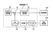
- FIG. 17 is a block diagram showing a configuration example of the control circuit 15 of FIG.
- the control circuit 15 includes a target voltage setter 20, a bandpass filter 21, a detector 22, an A / D converter 23, a subtractor 24, and a PWM signal generator 25.
- the control circuit 15 controls to correct the applied voltage V1 of the power supply device 12C so that the ripple current is minimized based on the current detection signal corresponding to the current detected by the current detector CS1.
- the current detection signal from the current detector CS1 is passed through the bandpass filter 21 and the detector 22 to detect the noise detection signal corresponding to the noise level, and the noise detection signal is digitally transmitted by the A / D converter. After converting to a signal, it is output to the subtractor 24.
- the subtractor 24 subtracts the digital signal of the noise detection signal from the target voltage signal from the target voltage setter 20, outputs the subtraction result signal to the PWM signal generator 25, and the PWM signal generator 25 subtracts the subtraction result.
- a PWM signal (gate control signal) having a duty ratio corresponding to the signal of is generated and applied to the gate driver of the switching circuit of the power supply device 12C.
- the control circuit 15 configured as described above executes feedback control for adjusting the duty ratio of the PWM signal (gate control signal) that generates the applied voltage V1 of the power supply device 12C from the comparison between the noise detection signal and the target voltage. ..
- the ripple component of the input current can be sufficiently suppressed.
- the power conversion device according to the present disclosure is useful for realizing a power conversion device used in in-vehicle equipment, industrial equipment, etc. with low noise, small size, and low cost.
Landscapes
- Engineering & Computer Science (AREA)
- Power Engineering (AREA)
- Dc-Dc Converters (AREA)
Priority Applications (3)
| Application Number | Priority Date | Filing Date | Title |
|---|---|---|---|
| JP2022568345A JP7784638B2 (ja) | 2020-12-11 | 2021-12-10 | 電力変換装置 |
| US18/255,304 US12431788B2 (en) | 2020-12-11 | 2021-12-10 | Power converter apparatus provided with ripple cancel current generator circuit |
| CN202180083396.9A CN116569464A (zh) | 2020-12-11 | 2021-12-10 | 电力转换装置 |
Applications Claiming Priority (2)
| Application Number | Priority Date | Filing Date | Title |
|---|---|---|---|
| JP2020-206190 | 2020-12-11 | ||
| JP2020206190 | 2020-12-11 |
Publications (1)
| Publication Number | Publication Date |
|---|---|
| WO2022124395A1 true WO2022124395A1 (ja) | 2022-06-16 |
Family
ID=81974594
Family Applications (1)
| Application Number | Title | Priority Date | Filing Date |
|---|---|---|---|
| PCT/JP2021/045518 Ceased WO2022124395A1 (ja) | 2020-12-11 | 2021-12-10 | 電力変換装置 |
Country Status (4)
| Country | Link |
|---|---|
| US (1) | US12431788B2 (https=) |
| JP (1) | JP7784638B2 (https=) |
| CN (1) | CN116569464A (https=) |
| WO (1) | WO2022124395A1 (https=) |
Families Citing this family (2)
| Publication number | Priority date | Publication date | Assignee | Title |
|---|---|---|---|---|
| US20240258929A1 (en) * | 2021-06-04 | 2024-08-01 | Mitsubishi Electric Corporation | Power converter and power supply apparatus |
| US12438442B1 (en) | 2024-10-23 | 2025-10-07 | Hong Kong Applied Science and Technology Research Institute Company Limited | Active variable inductor circuit |
Citations (6)
| Publication number | Priority date | Publication date | Assignee | Title |
|---|---|---|---|---|
| JP2011244534A (ja) * | 2010-05-14 | 2011-12-01 | Toyota Industries Corp | 電源回路 |
| JP2012147641A (ja) * | 2011-01-14 | 2012-08-02 | Sumitomo Heavy Ind Ltd | 電源装置 |
| CN103887958A (zh) * | 2014-04-03 | 2014-06-25 | 无锡中星微电子有限公司 | 直流-直流转换器 |
| US20200083798A1 (en) * | 2018-09-08 | 2020-03-12 | Shenzhen GOODIX Technology Co., Ltd. | Ripple detection and cancellation for voltage regulator circuits |
| WO2020053884A1 (en) * | 2018-09-10 | 2020-03-19 | INDIAN INSTITUTE OF TECHNOLOGY MADRAS (IIT Madras) | Ripple cancellation circuit in switching dc-dc converters and methods thereof |
| US20200321867A1 (en) * | 2017-12-22 | 2020-10-08 | Fraunhofer-Gesellschaft zur Förderung der angewandten Forschung e.V. | Voltage converter arrangement comprising an input regulating element, and method of operating a voltage converter arrangement |
Family Cites Families (12)
| Publication number | Priority date | Publication date | Assignee | Title |
|---|---|---|---|---|
| US5640315A (en) | 1994-03-18 | 1997-06-17 | Nippon Steel Corporation | Switching regulator |
| JPH07264849A (ja) | 1994-03-18 | 1995-10-13 | Nippon Steel Corp | スイッチングレギュレータ |
| JP3570113B2 (ja) | 1996-10-17 | 2004-09-29 | 松下電器産業株式会社 | インターリーブ方式スイッチングコンバータ |
| US5905369A (en) | 1996-10-17 | 1999-05-18 | Matsushita Electric Industrial Co., Ltd. | Variable frequency switching of synchronized interleaved switching converters |
| US6249108B1 (en) * | 1999-08-31 | 2001-06-19 | The Regents Of The University Of California | Unified constant-frequency integration control of active power filters |
| US6825643B2 (en) * | 2003-03-24 | 2004-11-30 | Micro-Star Int'l Co., Ltd. | Power converter module with an electromagnetically coupled inductor for switch control of a rectifier |
| FR2913827A1 (fr) * | 2007-03-13 | 2008-09-19 | Centre Nat Rech Scient | Dispositif de filtrage actif pour une alimentation de puissance |
| JP5937503B2 (ja) * | 2012-12-26 | 2016-06-22 | ルネサスエレクトロニクス株式会社 | 半導体集積回路およびその動作方法 |
| CN106100313A (zh) | 2015-04-27 | 2016-11-09 | 松下知识产权经营株式会社 | 电源电路 |
| US10050517B1 (en) * | 2017-01-31 | 2018-08-14 | Ricoh Electronics Devices Co., Ltd. | Power supply apparatus converting input voltage to predetermined output voltage and controlling output voltage based on feedback signal corresponding to output voltage |
| US11502594B2 (en) * | 2020-05-19 | 2022-11-15 | Analog Devices International Unlimited Company | Switched-mode power converter with ripple attenuation |
| CN115811210A (zh) * | 2022-12-07 | 2023-03-17 | 常州大学 | 一种提升级联功率变换器稳定性的电流纹波注入装置 |
-
2021
- 2021-12-10 US US18/255,304 patent/US12431788B2/en active Active
- 2021-12-10 CN CN202180083396.9A patent/CN116569464A/zh active Pending
- 2021-12-10 JP JP2022568345A patent/JP7784638B2/ja active Active
- 2021-12-10 WO PCT/JP2021/045518 patent/WO2022124395A1/ja not_active Ceased
Patent Citations (6)
| Publication number | Priority date | Publication date | Assignee | Title |
|---|---|---|---|---|
| JP2011244534A (ja) * | 2010-05-14 | 2011-12-01 | Toyota Industries Corp | 電源回路 |
| JP2012147641A (ja) * | 2011-01-14 | 2012-08-02 | Sumitomo Heavy Ind Ltd | 電源装置 |
| CN103887958A (zh) * | 2014-04-03 | 2014-06-25 | 无锡中星微电子有限公司 | 直流-直流转换器 |
| US20200321867A1 (en) * | 2017-12-22 | 2020-10-08 | Fraunhofer-Gesellschaft zur Förderung der angewandten Forschung e.V. | Voltage converter arrangement comprising an input regulating element, and method of operating a voltage converter arrangement |
| US20200083798A1 (en) * | 2018-09-08 | 2020-03-12 | Shenzhen GOODIX Technology Co., Ltd. | Ripple detection and cancellation for voltage regulator circuits |
| WO2020053884A1 (en) * | 2018-09-10 | 2020-03-19 | INDIAN INSTITUTE OF TECHNOLOGY MADRAS (IIT Madras) | Ripple cancellation circuit in switching dc-dc converters and methods thereof |
Also Published As
| Publication number | Publication date |
|---|---|
| CN116569464A (zh) | 2023-08-08 |
| US20240030804A1 (en) | 2024-01-25 |
| JP7784638B2 (ja) | 2025-12-12 |
| US12431788B2 (en) | 2025-09-30 |
| JPWO2022124395A1 (https=) | 2022-06-16 |
Similar Documents
| Publication | Publication Date | Title |
|---|---|---|
| US9537413B2 (en) | System for driving a piezoelectric load and method of making same | |
| RU2558945C2 (ru) | Сверхвысокоэффективный переключающий инвертор мощности и усилитель мощности | |
| EP2525482A1 (en) | Grid-tie inverter | |
| JP5304374B2 (ja) | 電力変換システムのノイズ低減法 | |
| CN115836469B (zh) | 电力转换装置及电力系统 | |
| JP7784638B2 (ja) | 電力変換装置 | |
| JP3296425B2 (ja) | 電力変換装置 | |
| US8629579B2 (en) | Active switching ripple filter | |
| JP2002359927A (ja) | フィルタ装置 | |
| JP2022050739A (ja) | 双方向絶縁型dc/dcコンバータおよびその制御方法 | |
| CN102393776A (zh) | 串联式交流稳压器 | |
| CN113348618A (zh) | 直流脉冲电源装置 | |
| Ohn et al. | A simplified digital closed-loop current control of three-phase PV inverter operating in triangular conduction mode | |
| JP2006238621A (ja) | 無停電電源装置 | |
| TW202137687A (zh) | 高頻電源裝置及高頻電源裝置的輸出控制方法 | |
| JP7219688B2 (ja) | 電力変換装置とその制御方法 | |
| Sani et al. | An extended coupled-inductor QZS inverter with high-frequency input current ripple suppression | |
| KR101230862B1 (ko) | 단일 전원으로 구동되는 멀티레벨 인버터 장치 | |
| CN113411003A (zh) | 双有源桥式变换器及其控制方法 | |
| Manikandan et al. | Implementation of high efficiency current-fed push-pull converter using soft switching technique | |
| JP5407515B2 (ja) | フィルタ回路とそれを用いた電力変換装置 | |
| JP2003230279A (ja) | 交流‐直流電力変換装置 | |
| EP4513732A1 (en) | Power conversion system and control method thereof | |
| JP7566158B2 (ja) | 電力変換装置 | |
| JP2004096911A (ja) | Pwmコンバータシステム |
Legal Events
| Date | Code | Title | Description |
|---|---|---|---|
| 121 | Ep: the epo has been informed by wipo that ep was designated in this application |
Ref document number: 21903491 Country of ref document: EP Kind code of ref document: A1 |
|
| ENP | Entry into the national phase |
Ref document number: 2022568345 Country of ref document: JP Kind code of ref document: A |
|
| WWE | Wipo information: entry into national phase |
Ref document number: 18255304 Country of ref document: US |
|
| WWE | Wipo information: entry into national phase |
Ref document number: 202180083396.9 Country of ref document: CN |
|
| NENP | Non-entry into the national phase |
Ref country code: DE |
|
| 122 | Ep: pct application non-entry in european phase |
Ref document number: 21903491 Country of ref document: EP Kind code of ref document: A1 |
|
| WWG | Wipo information: grant in national office |
Ref document number: 18255304 Country of ref document: US |