WO2022123633A1 - 柱状半導体メモリ装置とその製造方法 - Google Patents
柱状半導体メモリ装置とその製造方法 Download PDFInfo
- Publication number
- WO2022123633A1 WO2022123633A1 PCT/JP2020/045497 JP2020045497W WO2022123633A1 WO 2022123633 A1 WO2022123633 A1 WO 2022123633A1 JP 2020045497 W JP2020045497 W JP 2020045497W WO 2022123633 A1 WO2022123633 A1 WO 2022123633A1
- Authority
- WO
- WIPO (PCT)
- Prior art keywords
- layer
- conductor layer
- semiconductor column
- gate
- sgt
- Prior art date
- Legal status (The legal status is an assumption and is not a legal conclusion. Google has not performed a legal analysis and makes no representation as to the accuracy of the status listed.)
- Ceased
Links
Images










Classifications
-
- H—ELECTRICITY
- H10—SEMICONDUCTOR DEVICES; ELECTRIC SOLID-STATE DEVICES NOT OTHERWISE PROVIDED FOR
- H10B—ELECTRONIC MEMORY DEVICES
- H10B10/00—Static random access memory [SRAM] devices
- H10B10/12—Static random access memory [SRAM] devices comprising a MOSFET load element
- H10B10/125—Static random access memory [SRAM] devices comprising a MOSFET load element the MOSFET being a thin film transistor [TFT]
-
- H—ELECTRICITY
- H10—SEMICONDUCTOR DEVICES; ELECTRIC SOLID-STATE DEVICES NOT OTHERWISE PROVIDED FOR
- H10B—ELECTRONIC MEMORY DEVICES
- H10B10/00—Static random access memory [SRAM] devices
- H10B10/12—Static random access memory [SRAM] devices comprising a MOSFET load element
-
- H—ELECTRICITY
- H10—SEMICONDUCTOR DEVICES; ELECTRIC SOLID-STATE DEVICES NOT OTHERWISE PROVIDED FOR
- H10D—INORGANIC ELECTRIC SEMICONDUCTOR DEVICES
- H10D30/00—Field-effect transistors [FET]
- H10D30/01—Manufacture or treatment
- H10D30/021—Manufacture or treatment of FETs having insulated gates [IGFET]
- H10D30/025—Manufacture or treatment of FETs having insulated gates [IGFET] of vertical IGFETs
-
- H—ELECTRICITY
- H10—SEMICONDUCTOR DEVICES; ELECTRIC SOLID-STATE DEVICES NOT OTHERWISE PROVIDED FOR
- H10D—INORGANIC ELECTRIC SEMICONDUCTOR DEVICES
- H10D30/00—Field-effect transistors [FET]
- H10D30/60—Insulated-gate field-effect transistors [IGFET]
- H10D30/63—Vertical IGFETs
-
- H—ELECTRICITY
- H10—SEMICONDUCTOR DEVICES; ELECTRIC SOLID-STATE DEVICES NOT OTHERWISE PROVIDED FOR
- H10D—INORGANIC ELECTRIC SEMICONDUCTOR DEVICES
- H10D30/00—Field-effect transistors [FET]
- H10D30/60—Insulated-gate field-effect transistors [IGFET]
- H10D30/67—Thin-film transistors [TFT]
- H10D30/6729—Thin-film transistors [TFT] characterised by the electrodes
- H10D30/673—Thin-film transistors [TFT] characterised by the electrodes characterised by the shapes, relative sizes or dispositions of the gate electrodes
- H10D30/6735—Thin-film transistors [TFT] characterised by the electrodes characterised by the shapes, relative sizes or dispositions of the gate electrodes having gates fully surrounding the channels, e.g. gate-all-around
-
- H—ELECTRICITY
- H10—SEMICONDUCTOR DEVICES; ELECTRIC SOLID-STATE DEVICES NOT OTHERWISE PROVIDED FOR
- H10D—INORGANIC ELECTRIC SEMICONDUCTOR DEVICES
- H10D62/00—Semiconductor bodies, or regions thereof, of devices having potential barriers
- H10D62/10—Shapes, relative sizes or dispositions of the regions of the semiconductor bodies; Shapes of the semiconductor bodies
- H10D62/124—Shapes, relative sizes or dispositions of the regions of semiconductor bodies or of junctions between the regions
- H10D62/126—Top-view geometrical layouts of the regions or the junctions
-
- H—ELECTRICITY
- H10—SEMICONDUCTOR DEVICES; ELECTRIC SOLID-STATE DEVICES NOT OTHERWISE PROVIDED FOR
- H10D—INORGANIC ELECTRIC SEMICONDUCTOR DEVICES
- H10D30/00—Field-effect transistors [FET]
- H10D30/60—Insulated-gate field-effect transistors [IGFET]
- H10D30/67—Thin-film transistors [TFT]
- H10D30/6728—Vertical TFTs
-
- H—ELECTRICITY
- H10—SEMICONDUCTOR DEVICES; ELECTRIC SOLID-STATE DEVICES NOT OTHERWISE PROVIDED FOR
- H10D—INORGANIC ELECTRIC SEMICONDUCTOR DEVICES
- H10D89/00—Aspects of integrated devices not covered by groups H10D84/00 - H10D88/00
- H10D89/10—Integrated device layouts
Definitions
- the present invention relates to a columnar semiconductor memory device and a method for manufacturing the same.
- the channel In a normal planar MOS transistor, the channel extends horizontally along the upper surface of the semiconductor substrate.
- the channel of SGT extends in the direction perpendicular to the upper surface of the semiconductor substrate (see, for example, Patent Document 1 and Non-Patent Document 1). Therefore, the SGT can increase the density of the semiconductor device as compared with the planar type MOS transistor.
- FIG. 4 shows a schematic structural diagram of the N-channel SGT.
- Si column the silicon semiconductor column having a P-type or i-type (intrinsic type) conductive type, when one is the source, the other is the drain.
- N + layers 121a and 121b are formed (“N + layer” refers to a semiconductor region containing a high concentration of donor impurities; the same applies hereinafter).
- the portion of the Si column 120 between the N + layers 121a and 121b that serve as the source and drain becomes the channel region 122.
- the gate insulating layer 123 is formed so as to surround the channel region 122.
- the gate conductor layer 124 is formed so as to surround the gate insulating layer 123.
- the SGT is composed of N + layers 121a and 121b serving as sources and drains, a channel region 122, a gate insulating layer 123, and a gate conductor layer 124. It is opened in the insulating layer 125 on the N + layer 121b, and the N + layer 121b and the source wiring metal layer S are connected to each other via the contact hole C.
- the occupied area of the SGT corresponds to the occupied area of a single source or drain N + layer of the planar MOS transistor. Therefore, the circuit chip having the SGT can realize further reduction in the chip size as compared with the circuit chip having the planar type MOS transistor.
- a contact hole C connecting the source wiring metal layer S and the N + layer 121b is formed on the Si pillar 120 in a plan view.
- the distance between the Si pillar 120 and the adjacent Si pillar becomes shorter.
- an increase in the coupling capacitance between the electrodes of the adjacent SGTs and a decrease in the yield due to a short circuit between the electrodes of the adjacent SGTs become problems.
- FIG. 5 shows a SRAM cell (Static Random Access Memory) circuit diagram using SGT.
- This SRAM cell circuit includes two inverter circuits.
- One inverter circuit is composed of a P-channel SGT_Pc1 as a load transistor and an N-channel SGT_Nc1 as a drive transistor.
- the other inverter circuit is composed of a P channel SGT_Pc2 as a load transistor and an N channel SGT_Nc2 as a drive transistor.
- the gate of P channel SGT_Pc1 and the gate of N channel SGT_Nc1 are connected.
- the drain of the P channel SGT_Pc2 and the drain of the N channel SGT_Nc2 are connected.
- the gate of P channel SGT_Pc2 and the gate of N channel SGT_Nc2 are connected.
- the drain of the P channel SGT_Pc1 and the drain of the N channel SGT_Nc1 are connected.
- the sources of the P channels SGT_Pc1 and Pc2 are connected to the power supply terminal Vdd.
- the sources of the N channels SGT_Nc1 and Nc2 are connected to the ground terminal Vss.
- Selected N channels SGT_SN1 and SN2 are arranged on both sides of the two inverter circuits.
- the gates of the selected N channels SGT_SN1 and SN2 are connected to the word line terminal WLt.
- the source and drain of the selected N channel SGT_SN1 are connected to the drain of the N channel SGT_Nc1 and the P channel SGT_Pc1 and the bit line terminal BLt.
- the source and drain of the selected N channel SGT_SN2 are connected to the drain of the N channel SGT_Nc2 and the P channel SGT_Pc2 and the inverted bit line terminal BLRt.
- the circuit having the SRAM cell is composed of two load P channels SGT_Pc1 and Pc2, two driving N channels SGT_Nc1 and Nc2, and two selection SN1 and SN2 from a total of six SGTs. It is configured (see, for example, Patent Document 2).
- this SRAM cell how to reduce the parasitic capacitance between each electrode and the connection wiring is an issue. At the same time, it is also an issue how to reduce the defects caused by the short circuit between the electrodes due to the high density of the SRAM cell.
- the method for manufacturing a columnar semiconductor memory device of the present invention is: On the substrate, a first semiconductor column that is aligned on the first line in a plan view and forms a first SGT (Surrounding Gate Transistor) standing in a vertical direction, and adjacent to the first semiconductor column, A second semiconductor column forming a second SGT and a third semiconductor column forming a third SGT that is aligned on a second line parallel to the first line in a plan view and stands vertically. And a step of forming a fourth semiconductor column that forms a fourth SGT adjacent to the third semiconductor column.
- SGT Standard Gate Transistor
- the third gate insulating layer was surrounded, and in plan view, the third gate conductor layer protruding in the direction of the first line and the fourth gate insulating layer were surrounded.
- a first contact hole is formed on the third gate conductor layer protruding from the third semiconductor column, and at the same time, a third impurity region at the bottom of the third semiconductor column and the fourth semiconductor column.
- a second contact hole is formed on the second connection region connecting the fourth impurity region at the bottom and the second gate conductor layer protruding in the second line direction in a plan view.
- a first insulating material layer made of a first pore or a low dielectric constant material layer is formed, and at the same time, the said on the second conductor layer. It comprises a step of forming a second insulating material layer composed of a second pore or a low dielectric constant material layer in the second contact hole.
- the first SGT and the fourth SGT are selection transistors of the SRAM memory cell, and the second SGT and the third SGT are load transistors of the SRAM memory cell.
- the upper end positions of the first hole and the second hole are the first gate conductor layer, the second gate conductor layer, and the third gate conductor layer. It is desirable to form it lower than the upper end position of the fourth gate conductor layer.
- the thickness of the second gate conductor layer in the region in contact with the second contact hole is set to the thickness of the second gate conductor layer surrounding the second gate insulating layer. It is desirable to form it thicker than the thickness of the gate conductor layer.
- the first gate insulating layer, the second gate insulating layer, the third gate insulating layer, and the fourth gate insulating layer are further surrounded, and the upper surface position is positioned in the vertical direction.
- the second mask material layer is connected to the second semiconductor column and partly protrudes in the second line direction, and is connected to the third semiconductor column and partly connected to the first semiconductor column.
- the film thickness of the second gate conductor layer overlapping with the second mask material layer is formed to be thicker than the film thickness of the first mask material layer
- the third The thickness of the third gate conductor layer that overlaps with the mask material layer is formed to be thicker than the film thickness of the third mask material layer.
- the columnar semiconductor memory device of the present invention is used.
- a first semiconductor column that is aligned on the first line in a plan view and forms a first SGT (Surrounding Gate Transistor) standing in a vertical direction, and adjacent to the first semiconductor column,
- a second semiconductor column forming a second SGT, a third semiconductor column arranged on a second line parallel to the first line in a plan view and standing in a vertical direction, and the third semiconductor.
- a fourth semiconductor column that forms a fourth SGT adjacent to the column, A first gate insulating layer surrounding the first semiconductor column, a second gate insulating layer surrounding the second semiconductor column, and a third gate insulating layer surrounding the third semiconductor column.
- the third gate insulating layer was surrounded, and in plan view, the third gate conductor layer protruding in the direction of the first line and the fourth gate insulating layer were surrounded.
- a first insulating material layer made of a first pore or a low dielectric constant material layer in the first contact portion on the first conductor layer, and the second on the second conductor layer.
- the first SGT and the fourth SGT are the selection transistors of the SRAM memory cell, and the second SGT and the third SGT are the load transistors of the SRAM memory cell.
- the upper end positions of the first hole and the second hole are the first gate conductor layer, the second conductor layer, the third gate conductor layer, and the above. It is characterized in that it is lower than the upper end position of the fourth gate conductor layer.
- the region in contact with the second contact hole is characterized in that the thickness of the second gate conductor layer is thicker than the thickness of the second gate conductor layer surrounding the second gate insulating layer.
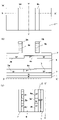
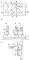
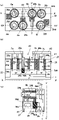
- FIGS. 1A to 1U (First Embodiment)
- a is a plan view
- (b) is a cross-sectional structure diagram along the XX'line of (a)
- (c) is a cross-sectional structure diagram along the YY'line of (a). ..
- the N layer 2 is formed on the P layer substrate 1 (which is an example of the “substrate” in the claims) by the epitaxial crystal growth method.
- N + layer 3a and P + layer (“P + layer” refers to a semiconductor region containing a high concentration of acceptor impurities; the same applies hereinafter) 4a and 4b are added to the surface layer of N layer 2 by the epitaxial crystal growth method, respectively.
- the i-layer 6 is formed.
- N + layer 3b, P + layer 4c, and 4d are formed on the i-layer 6 by the epitaxial crystal growth method.
- a mask material layer 7 composed of a SiO 2 layer, an aluminum oxide (Al 2 O 3 , hereinafter referred to as AlO) layer, and a SiO 2 layer is formed.
- AlO aluminum oxide
- SiO 2 layer silicon germanium
- the mask material layer 9 composed of the SiO 2 layer and the SiN layer is deposited.
- the i-layer 6 may be formed of N-type or P-type Si containing a small amount of donor or acceptor impurity atoms.
- the N + layer 3a, 3b, P + layer 4a, 4b, 4c, and 4d may be formed by another method such as an ion implantation method.
- the mask material layer 9 may be formed of a single layer containing a SiO 2 layer, a SiN layer, or another material layer, or a plurality of material layers.
- the mask material layer 9 is etched by the RIE (Reactive Ion Etching) method using the strip-shaped resist layer (not shown) stretched in the Y direction as a mask in the plan view formed by the lithography method. Then, using the resist layer as a mask, the mask material layer 9 is isotropically etched to form band-shaped mask material layers 9a and 9b. As a result, the widths of the band-shaped mask material layers 9a and 9b are formed to be narrower than the width of the minimum resist layer that can be formed by the lithography method. Next, using the band-shaped mask material layers 9a and 9b as masks, the SiGe layer 8 is etched by, for example, the RIE method to form the band-shaped SiGe layers 8a and 8b as shown in FIG. 1B.
- the RIE Reactive Ion Etching
- a SiN layer (not shown) is formed so as to cover the mask material layer 7, the band-shaped SiGe layers 8a and 8b, and the band-shaped mask material layers 9a and 9b by the ALD (Atomic Layered Deposition) method.
- the cross section of the SiN layer is rounded at the top. It is desirable that this roundness is formed so as to be above the band-shaped SiGe layers 8a and 8b.
- the whole is covered with, for example, a SiO 2 layer (not shown) by a flow CVD (Flow Chemical Vapor Deposition) method, and the upper surface position is a band-shaped mask material layer 9a, 9b upper surface by CMP (Chemical Mechanical Polishing).
- the SiO 2 layer and the SiN layer are polished so as to be in the position to form the SiN layers 13a, 13b and 13c. Then, the tops of the SiN layers 13a, 13b, and 13c are etched to form recesses. The bottom of the recess is formed so as to be at the lower position of the band-shaped mask material layers 9a and 9b. Then, the entire SiN layer (not shown) is coated, and the entire surface is polished by the CMP method so that the upper surface positions are the upper surface positions of the mask material layers 9a and 9b. Then, the SiO 2 layer formed by the flow CVD is removed. As a result, as shown in FIG.
- the band-shaped mask material layers 12aa, 12ab, 12ba, 12bb having the same shape as the top shape of the SiN layers 13a, 13b, 13c in a plan view on both sides of the band-shaped mask material layers 9a, 9b. Is formed.
- the strip-shaped SiN layers 13a, 13ab, 13ba are etched with the strip-shaped mask material layers 9a, 9b, 12aa, 12ab, 12ba, 12bb as masks and the SiN layers 13a, 13b, 13c are etched. , 13bb.
- the widths of the strip-shaped SiN layers 13aa, 13ab, 13ba, and 13bb are the same in a plan view.
- band-shaped mask material layers 9a and 9b and the band-shaped SiGe layers 8a and 8b are removed.
- strip-shaped mask material layers 12aa, 12ab, 12ba, and 12bb extending in the Y direction in a plan view and arranged in parallel with each other are placed on the tops of the mask material layers 7.
- the strip-shaped SiN layers 13aa, 13ab, 13ba, 13bb having the same are formed.
- the entire surface is covered to form a SiO 2 layer (not shown) by the flow CVD method.
- the SiO 2 layer is polished so that the upper surface position thereof is the same as the upper surface position of the band-shaped mask material layers 12aa, 12ab, 12ba, 12bb, and the SiO 2 layer is polished as shown in FIG. 1F.
- the SiN layer 16 is formed on the SiO 2 layer 15, the band-shaped mask material layers 12aa, 12ab, 12ba, and 12bb.
- the strip-shaped mask material layers 17a extending in the X direction on the SiN layer 16 and arranging in parallel with each other. , 17b.
- the strip-shaped mask material layers 17a and 17b are used as masks, and the SiN layer 16, the strip-shaped mask material layers 12aa, 12ab, 12ba, 12bb, the strip-shaped SiN layers 13aa, 13ab, 13ba, 13bb, and the mask.
- the material layer 7 is RIE etched.
- the remaining SiN layer 16 and SiO 2 layer 15 are removed.
- the SiN columns 20a, 20b, 20c, 20d, 20e, 20f, 20g, 20h having the rectangular mask material layers 19a, 19b, 19c, 19d, 19e, 19f, 19g, 19h at the top are formed.
- the mask material layer 19a, 19c, 19d, 19e, 19f, 19h and the SiN pillars 20a, 20c, 20d, 20e, 20f, 20h are used as masks, and the mask material layer 7 is etched and shown in FIG. 1I.
- the mask material layers 7a, 7b, 7c, 7d, 7e, and 7f are formed.
- the shapes of the mask material layers 7a, 7b, 7c, 7d, 7e, and 7f are made into a circular shape in a plan view.
- This CDE etching is not necessary when the plan view shape of the mask material layers 7a, 7b, 7c, 7d, 7e, and 7f is circular before this step. Then, the mask material layers 19a, 19c, 19d, 19e, 19f, 19h and the SiN columns 20a, 20c, 20d, 20e, 20f, 20h are removed. Then, as shown in FIG. 1I, the mask material layers 7a, 7b, 7c, 7d, 7e, and 7f are used as masks, and the N + layer 3b, P + layer 4c, 4d, and i layer 6 are etched to N +.
- Si columns 6a (an example of the "first semiconductor column” in the claims) and 6b (an example of the “second semiconductor columns” in the claims) on layers 3a, P + layers 4a and 4b. Yes), 6c, 6d, 6e (an example of the "third semiconductor pillar” in the claims), 6f (an example of the "fourth semiconductor pillar” in the claims).
- Si columns 6a, 6b, 6c are formed on the XX'line (an example of the "first line” in the claims), and the XX-XX'line (the "second line” in the claims) is formed.
- Si columns 6d, 6e, 6f are formed on the line).
- N + layer 3ba is on the top of the Si pillar 6a
- P + layer 4ca is on the top of the Si pillar 6b
- N + layer 3bb is on the top of the Si pillar 6c
- N + layer 3Ba is on the top of the Si pillar 6d (shown).
- a P + layer 4Ca (not shown) is formed on the top of the Si pillar 6e
- an N + layer 3Bb (not shown) is formed on the top of the Si pillar 6f.
- N + layer 3a, P + layer 4a, N layer 2, and P layer substrate 1 connected to the bottoms of the Si columns 6a, 6b, and 6c are etched to form the upper portion of the P layer substrate 1.
- N layer 2a, N + layer 3aa (an example of the "first impurity layer” in the claims), 3ab, P + layer 4aa (an example of the "second impurity layer” in the claims).
- Si pillar base 21a There is) to form a Si pillar base 21a.
- the HfO 2 layer 23 and the TiN layer are formed by covering the whole by the ALD method.
- the TiN layers are in contact with each other between the Si columns 6b and 6c and between the Si columns 6d and 6e.
- the TiN layer 24a (the "first gate” in the claims) surrounds the HfO 2 layer 23 (an example of the "first gate insulating layer” in the claims) surrounding the outer periphery of the Si column 6a.
- An example of a “conductor layer”) is surrounded by an HfO 2 layer 23 (an example of a "second gate insulating layer” in the claims) on the outer periphery of the Si columns 6b and 6c, and a TiN layer 24b (patent claim).
- HfO 2 layer 23 an example of a "second gate insulating layer” in the claims
- TiN layer 24b pattern claim
- the entire surface is covered with a SiO 2 layer (not shown), and then the entire surface is subjected to the CMP method so that the upper surface position thereof is the upper surface position of the mask material layers 7a, 7b, 7c, 7d, 7e, 7f. Polish to.
- the SiO 2 layer (not shown) flattened by the RIE method is etched back to form the SiO 2 layer 25.
- the tops of the HfO 2 layer 23 and the TiN layers 24a, 24b, 24c, 24d are removed.
- the TiN layers 24a, 24b, 24c, and 24d serve as SGT gate conductor layers.
- This gate conductor layer is a layer that contributes to the setting of the threshold voltage of the SGT, and may be formed from a single layer or a gate conductor layer composed of a plurality of layers.
- the gate conductor material layer is formed in contact with the entire side surface between the Si columns 6b and 6c and between the Si columns 6d and 6e.
- This W layer may be another conductor material layer.
- the HfO 2 layer 23 may be formed by changing the film thickness or the material in the Si columns 6a to 6f. Further, the SiO 2 layer 25 may be formed so that the upper surface thereof is above the upper surface positions of the TiN layers 24a to 24d.
- the SiN layer 27 is formed on the SiO 2 layer 25 on the outer peripheral portion of the Si columns 6a to 6f. Then, the entire SiO 2 layer (not shown) is covered. Then, by etching the SiO 2 layer by the RIE method, the top of the exposed Si columns 6a to 6f and the side surfaces of the mask material layers 7a to 7f are exposed to the SiO 2 layer 28a having the same width in a plan view. , 28b, 28c, 28d, 28e, 28f. In this case, the SiO 2 layer 28b and the SiO 2 layer 28c are formed apart from each other. Similarly, the SiO 2 layer 28d and the SiO 2 layer 28e are formed apart from each other.
- the SiN layer 27 may be formed on at least the TiN layers 24a, 24b, 24c, and 24d, which are gate conductor layers. Further, when the SiO 2 layer 25 is formed of the SiN layer and the upper surface thereof is formed so as to be above the upper surface position of the TiN layers 24a to 24d, the SiN layer 27 may not be formed.
- AlO aluminum oxide
- the AlO layer 29 is formed by polishing so that the upper surface position of the AlO layer is the upper surface position of the mask material layers 7a to 7f by the CMP method.
- the SiO 2 layers 28a, 28b, 28c, 28d, 28e, 28f surrounding the tops of the Si columns 6a to 6f are removed, and the recesses 30a, 30b, 30c, 30d surrounding the tops of the Si columns 6a to 6f are removed. 30e and 30f are formed.
- the AlO layer 29 may be formed of a single layer or a plurality of other material layers.
- the mask material layers 7a, 7b, 7c, 7d, 7e, and 7f are removed, and the recesses 30A, 30B, 30C, and 30D are formed on the outer periphery and the upper portion of the tops of the Si columns 6a to 6f. 30E and 30F are formed.
- the order of removing the SiO 2 layers 28a, 28b, 28c, 28d, 28e, 28f and the mask material layers 7a, 7b, 7c, 7d, 7e, 7f may come first.
- the entire SiO 2 layer (not shown) is coated by the CVD method.
- the upper surface position of the SiO 2 layer is polished to the upper surface position of the AlO layer 29 by the CMP method to cover the tops of the Si columns 6a to 6f, and the recesses 30A, 30B, 30C.
- SiO 2 layers 31a, 31b (not shown) 31c, 31d, 31e (not shown), 31f are formed in 30D, 30E, 30F.
- the SiO 2 layers 31b and 31e are removed by a lithography method and a chemical etching method.
- the P + layers 32b and 32e containing acceptor impurities are formed in the recesses 30B and 30E so as to cover the tops of the Si columns 6b and 6e by the selective epitaxial crystal growth method.
- the outer circumferences of the P + layers 32b and 32e are formed so as not to be outside the outer circumferences of the recesses 30B and 30E in a plan view.
- the tops of the Si columns 6b and 6e are thinly oxidized, and then a treatment for removing the oxide film is performed to remove the damaged layer on the top surface of the Si columns 6b and 6e. And cleaning is desirable.
- the P + layer 32b, 32e may form a single crystal P + layer 32b, 32e by using a method other than the selective epitaxial crystal growth method, for example, a molecular beam crystal growth method. Further, the P + layers 32b and 32e are coated with a semiconductor layer containing acceptor impurities on the entire surface, and then polished to the upper surface position of the AlO layer 29 by the CMP method, and then the upper surface is subjected to the CDE method or chemicals. It may be formed by etching.
- the entire SiO 2 layer (not shown) is coated and polished by the CMP method so that the upper surface position of the SiO 2 layer is the same as the upper surface position of the AlO layer 29, and the P + layer 32b, A SiO 2 layer (not shown) is coated on the 32e.
- the SiO 2 layers 31a, 31c, 31d, and 31f are removed by a lithography method and chemical etching.
- the N + layers 32a, 32c, 32d, 32f containing the donor impurities are covered with the tops of the Si columns 6a, 6c, 6d, 6f by the selective epitaxial crystal growth method, and the recesses 30A, It is formed in 30C, 30D, and 30F.
- the outer circumferences of the N + layers 32a, 32c, 32d, and 32f are formed so as not to be outside the outer circumferences of the recesses 30A, 30C, 30D, and 30F in a plan view. Then, the SiO 2 layer on the P + layers 32b and 32e is removed.
- a thin Ta layer (not shown) and a W layer (not shown) are coated on the whole.
- the W layer is polished so that the upper surface position of the W layer is the upper surface position of the AlO layer 29 by the CMP method, and the W layers 33a, 33b, 33c, 33d having Ta layers on the side surfaces and the bottom surface. , 33e, 33f are formed.
- the Ta layer between the N + layers 32a, 32c, 32d, 32f, P + layers 32b, 32e and the W layers 33a, 33b, 33c, 33d, 33e, 33f is of these two layers.
- It is a buffer layer for reducing contact resistance.
- This buffer layer may be a single layer or a plurality of other material layers.
- the region including the boundary between N + layer 3aa and P + layer 4aa (which is an example of the "first connection region” in the claims) and the TiN layer 24c.
- a contact hole C1 (an example of a "first contact hole” in the claims) is formed on the contact hole C1.
- the contact hole C2 (which is an example of the "second connection region” in the claims), the TiN layer 24b, and the region including the boundary between the N + layer 3bB and the P + layer 4bb (is an example). It forms an example of a "second contact hole” in the claims).
- etch back is performed by RIE so that the upper surface position of the W layer is lower than the upper surface position of the contact holes C1 and C2, and the W layer 34a (claimed) is formed in the contact holes C1 and C2.
- a SiO2 layer is deposited on the contact holes C1 and C2 on the W layers 34a and 34b and on the AlO layer 29 by a CVD (Chemical Vapor Deposition) method.
- the SiO2 layer is polished so that the upper surface thereof becomes the upper surface of the AlO layer 29, and the holes 36a (the "first holes” in the claims) are formed on the W layers 34a and 34b. ), 36b (an example of a “second hole” in the claims), SiO2 layer 35a (an example of a "first insulating material layer” in the claims), 35b. (An example of the "second insulating material layer” in the claims) is formed.
- the upper surface positions of the W layers 34a and 34b are formed so as to be below or near the lower end positions of the gate TiN layers 24a to 24d in the vertical direction.
- another conductor layer may be used instead of the buffer Ti layer.
- another conductor material layer may be used instead of the W layers 34a and 34b.
- the conductor layer corresponding to the W layers 34a and 34b may be directly formed without using the buffer conductor layer.
- the entire surface is covered with two layers of SiO (not shown).
- SiO 2 layer 37 As shown in FIG. 1S, after forming the SiO 2 layer 37 as a whole, at least one of the W layers 33b and 33e on the Si columns 6b and 6e is used in a plan view by using a lithography method and a RIE method. It overlaps with the portion and forms a band-shaped contact hole C3 extending in the Y direction. The bottom of the strip-shaped contact hole C3 may reach the upper surface of the SiN layer 27.
- the band-shaped contact C3 is filled to form a power supply wiring metal layer Vdd in which the W layer 33b and 33e are connected.
- the power supply wiring metal layer Vdd may be formed by using a single layer or a plurality of layers of a material made of a semiconductor containing a large amount of alloys, donors or acceptor impurities as well as metals.
- a SiO 2 layer 38 having a flat upper surface is formed so as to cover the whole.
- the ground wiring metal layer Vss1 is formed via the contact hole C4 formed on the W layer 33c on the N + layer 32c.
- the ground wiring metal layer Vss2 is formed via the contact hole C5 formed on the W layer 33d on the N + layer 32d.
- a SiO 2 layer 39 having a flat upper surface is formed so as to cover the whole.
- the word wiring metal layer WL is formed through the contact holes C6 and C7 formed on the TiN layers 24a and 24d.
- the SiO 2 layer 40 having a flat upper surface is formed so as to cover the whole.
- the inverted bit output wiring metal layer RBL and the bit output wiring metal layer BL are formed via the contact holes C8 and C9 formed in the W layers 33a and 33f on the N + layers 32a and 32f.
- the SRAM cell circuit is formed on the P layer substrate 1.
- a selection transistor SGT an example of the "first SGT” in the scope of the patent claim
- a load transistor SGT the second SGT in the scope of the patent claim
- SGT drive transistor SGT
- Si column 6c a drive transistor SGT is formed on the Si column 6d
- a load transistor SGT the third in the scope of the patent claim
- Si column 6e a load transistor SGT (the third in the scope of the patent claim) is formed on the Si column 6e.
- SGT selection transistor SGT
- a load SGT is formed on the Si columns 6b and 6e
- a drive SGT is formed on the Si columns 6c and 6d
- a selection SGT is formed on the Si columns 6a and 6f.
- the SiO 2 layers 35a and 35b including the pores 36a and 36b are effectively low dielectric constant material layers.
- another low dielectric constant material layer containing or not containing the pores 36a and 36b may be used instead of the SiO 2 layers 35a and 35b.
- a SiN layer by, for example, a CVD method, a large volume of pores is formed, thereby forming an effective low dielectric constant material layer in the contact holes C1 and C2. You may.
- the holes 36a and 36b are the SiO 2 layers 35a. , 35b, the upper end positions of the holes 36a, 36b may be higher than the upper ends of the gate TiN layers 24a to 24d.
- the W layer 34a is in direct contact with the N + layer 3aa and the P + layer 4aa, but for example, on the N + layer 3aa and the P + layer 4aa between the Si columns 6a and 6b in a plan view, for example.
- a conductor layer such as a metal or a silicide layer may be provided, and the contact hole C1 may be formed on the conductor layer. This also applies to the contact hole C2.
- the P layer substrate 1 is used as the substrate.
- the N layer 2 on the P layer substrate 1 may also include the substrate as a part.
- another substrate such as, for example, SOI (Silicon Oxide Insulator) may be used.
- the N + layer 3aa, 3ab, 3aB, 3bB, P + layer 4aa, 4bb may be formed by connecting to the bottom side surface of the Si columns 6a to 6f.
- the N + layer 3aa, 3ab, 3aB, 3bB, P + layer 4aa, 4bb, 4ca, and 4Ca serving as the source or drain of the SGT are inside the bottom or top of the Si columns 6a to 6f, or. It may be in contact with the outside of the side surface and may be formed on the outer periphery thereof, and each may be electrically connected by another conductor material.
- (Feature 1) The W layer 34a connecting the N + layer 3aa, the P + layer 4aa, and the gate TiN layer 24c between the Si columns 6a and 6b on which the selective SGT and the load SGT are formed, as shown in FIG. 1U, and an effective low dielectric.
- the SiO 2 layer 35a which is a rate layer, is formed in the contact hole C1.
- the W layer 24a and the SiO2 layer 24a are formed by self-alignment.
- the W layer 24b and the SiO2 layer 24b are formed by self-alignment. This self-alignment formation leads to high integration of SRAM cells.
- the SiO 2 layer 35a including the holes 36a reduces the coupling capacitance between the gate TiN layer 24a of the selected SGT and the gate TiN layer 24b of the load SGT and the drive SGT.
- the SiO 2 layer 35b including the pores 36b reduces the coupling capacitance between the gate TiN layer 24d of the selective SGT and the gate TiN layer 24c of the load SGT. This reduction in coupling capacity leads to higher speed and lower power consumption of the SRAM device.
- the W layer 34a is formed so that the upper surface thereof is below or near the lower end positions of the gate TiN layers 24a to 24d in the vertical direction.
- the side surface of the W layer 34a can be formed with a small area facing the side surface of the gate TiN layers 24a and 24b, or separated from the side surface.
- short-circuit defects between the W layer 34b and the gate TiN layers 24c and 24d can be reduced. This contributes to the improvement of the yield of the SRAM device.
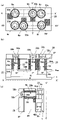
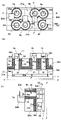
- FIGS. 2A and 2B (Second Embodiment) Hereinafter, a method for manufacturing an SRAM cell circuit having an SGT according to a second embodiment of the present invention will be described with reference to FIGS. 2A and 2B.
- (A) is a plan view
- (b) is a cross-sectional structure diagram along the XX'line of (a)
- (c) is a cross-sectional structure diagram along the YY'line of (a).
- the steps from FIG. 1A to FIG. 1R described in the first embodiment are performed.
- the entire surface is covered with a resist layer (not shown).
- the SiN layer 41, the mask material layers 7a to 7f, and the SiO 2 layers 28a to 28f are overlapped with the Si columns 6b and 6e in a plan view and have a strip shape.
- the vacant resist layer 42 is formed.
- the SiN layer 41, the mask material layers 7b, 7e, and the SiO 2 layers 28b, 28e, 35a, and 35b are placed above the top surface positions of the Si columns 6b, 6e.
- the recess 43 is formed by etching by the RIE method so as to be. In a plan view, the recess 43 partially overlaps with the SiO 2 layers 35a and 35b. The bottom of the recess 43 may reach the SiN layer 27. Further, as the resist layer 42, a single layer or another material layer composed of a plurality of layers may be used as long as it serves as an etching mask.
- the resist layer 42 is removed.
- the mask material layers 7b and 7e on the Si columns 6b and 6e and the SiO 2 layers 28b and 28e are removed.
- a thin single crystal Si layer (not shown) by the ALD method and a P + layer (not shown) containing acceptor impurities by the epitaxial crystal growth method are coated on the whole.
- the P + layer and the thin Si layer are polished so that the upper surface position thereof is the upper surface position of the SiN layer 41, and the thin single crystal Si layer 45b and the P + layer 46b are formed into the P + layer as shown in FIG. 2B. It is formed on 4ca and 4Ca.
- N + layers 46a, 46c, 46d, 46f are formed on N + layers 3ba, 3bb, 3Ba, and 3Bb. Then, the upper surface of the P + layer 46b, 46e, N + layer 46a, 46c, 46d, 46f is etched so as to be lower than the upper surface of the SiN layer 41. Then, the W layers 49a, 49b, 49c, 49d, 49e are formed on the P + layers 46b, 46e, N + layers 46a, 46c, 46d, 46f. Here, the upper end positions of the holes 36a and 36b in the vertical direction are formed so as to be below the SiN layer 27. Next, by performing the process shown in FIG. 1T, the SRAM cell circuit is formed on the P layer substrate 1.
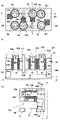
- FIGS. 3A to 3C are plan views
- (b) is a cross-sectional structure diagram along the XX'line of (a)
- (c) is a cross-sectional structure diagram along the YY'line of (a).
- the steps up to FIG. 1I in the first embodiment are performed. Then, the entire surface is covered, an HfO 2 layer (not shown) and a TiN layer (not shown) are deposited using ALD (Atomic Layered Deposition), and a SiO 2 layer (not shown) is formed by the CVD method. accumulate. Then, by the CMP method, the upper surfaces of the HfO 2 layer, the TiN layer, and the SiO 2 layer are polished so as to be at the upper surface positions of the mask material layers 7a to 7f.
- ALD Advanced Layered Deposition
- the TiN layer and the SiO2 layer are etched by the RIE method to the vicinity of the lower end position of the N + layer 3ba, 3bb, 3Ba, 3Bb, P + layer 3bb, 3Ca.
- the TiN layer 24 and the SiO2 layer 25A are formed.
- a SiN layer (not shown) is deposited on the entire surface.
- the SiN layer 26b is formed by being connected between the P + layer 4ca and the N + layer 3bb.
- the SiN layer 26c is formed by connecting the P + layer 4ca and the N + layer 3Ba.
- the mask material layer 26A partially overlapped with the SiN layer 26a
- the mask material layer 26B partially overlapped with the SiN layer 26b
- the mask material layer 26C partially overlapped with the SiN layer 26c
- the SiN layer 26d A partially overlapping mask material layer 26D is formed.
- the thickness L1 of the mask material layers 26a to 26f in a plan view is made smaller than the thickness L2 of the TiN layer.
- the SiO 2 layer 25A and the TiN layer 24 are etched by using the mask material layers 7a to 7d and 26A to 26D and the SiN layers 26a to 26d as masks, and the TiN layers 24A and 24B are etched. , 24C, 24D.
- the SiO2 layer 25A below the mask material layers 26A to 26D is left.
- the thickness of the TiN layers 24A to 24D surrounding the Si columns 6a to 6f is formed as thin as L1 while the thickness L2 of the bottom of the TiN layers 24A to 24D is maintained.
- SiO 2 layers 35a and 35b including the holes 36a and 36b are formed on the W layers 34a and 34b.
- the W layers 34a and 34b are formed on the bottom of the contact holes C1 and C2 (see FIG. 1Q).
- the contact holes C1 and C2 are formed on the thick TiN layers 24B and 24C having a thickness of L2.
- the SRAM cell is formed on the P layer substrate 1.
- the thickness of the gate TiN layers 24A to 24D may be about 2 to 5 nm as long as a predetermined work function can be obtained.
- the thinner the gate TiN layers 24A to 24D the better.
- the contact holes C1 and C2 may penetrate the TiN layers 24B and 24C when the contact holes C1 and C2 are formed. In this case, there is a high possibility that poor connection between the TiN layers 24B and 24C and the W layers 34a and 34b will occur.
- the thickness of the TiN layers 24A to 24D on the outer peripheral portion of the Si columns 6a to 6f is reduced to the thickness of the TiN layers 24B and 24C in the portions in contact with the contact holes C1 and C2. It can be thickened. This makes it possible to prevent poor connection between the TiN layers 24B and 24C and the W layers 34a and 34b.
- a logic circuit is formed around the SRAM cell region. In this logic circuit, a plurality of SGTs are connected by conductor electrodes. As the conductor electrode, a TiN layer having the same thickness as the thick TiN layers 24B and 24C connected to the W layers 34a and 34b is used.
- the TiN layer is required to have low resistance. From this point of view, it is necessary to increase the thickness of the TiN layer. On the other hand, even in the SGT in the logic circuit region, it is desirable that the gate TiN layer in the portion surrounding the Si column is thin for high integration. On the other hand, this embodiment contributes to high integration and high performance even in the SGT in the logic circuit region.
- one SGT is formed on one semiconductor column, but the present invention can also be applied to the formation of a circuit in which two or more SGTs are formed.
- the present invention can be applied to the connection between the top impurity layers of the SGT at the top of two semiconductor columns forming two or more SGTs.
- the Si columns 6a to 6f are formed in the first embodiment, the semiconductor columns may be made of other semiconductor materials. This also applies to the other embodiments according to the present invention.
- an SRAM cell composed of 6 SGTs has been described as an example.
- the present invention can be applied as long as the region where the contact hole C1 is formed between the Si columns 6a and 6b and the contact hole C2 is formed between the Si columns 6e and 6f is included. This also applies to the other embodiments according to the present invention.
- the N + layer 32a, 32c, 32d, 32f, P + layer 32b, 32e in the first embodiment may be formed of a donor, Si containing acceptor impurities, or another semiconductor material layer. Further, the N + layers 32a, 32c, 32d, 32f and the P + layers 32b, 32e may be formed from different semiconductor material layers. This also applies to the other embodiments according to the present invention.
- the AlO layer 29 surrounding the SiO 2 layers 28a to 28f another material layer including an organic material or an inorganic material composed of a single layer or a plurality of layers may be used as long as it is a material suitable for the object of the present invention. .. This also applies to the other embodiments according to the present invention.
- the mask material layer 7 is formed of a SiO 2 layer, an AlO layer, and a SiO 2 layer.
- any other material layer including an organic material or an inorganic material composed of a single layer or a plurality of layers may be used as long as it is a material suitable for the object of the present invention. This also applies to the other embodiments according to the present invention.
- strip-shaped SiN layers 13aa, 13ab, 13ba, and 13bb formed by the ALD method were formed on both sides of the strip-shaped SiGe layers 8a and 8b.
- the band-shaped SiN layers 13aa, 13ab, 13ba, 13bb and the band-shaped SiGe layers 8a, 8b are other material layers including an organic material or an inorganic material consisting of a single layer or a plurality of layers as long as they are materials suitable for the object of the present invention. May be used. This also applies to the other embodiments according to the present invention.
- N + layers 3aa, 3ab, 3ba, 3bb, P + layers 4aa, 4bb which are sources or drains of SGT, are N in the lower part of the Si columns 6a to 6f. They were connected and formed on layers 2a and 2b.
- N + layers 3aa, 3ab, 3ba, 3bb, P + layers 4aa, 4bb are formed on the bottoms of Si columns 6a to 6f
- N + layers 3aa, 3ab, 3ba, 3bb, P + layers. 4aa and 4bb may be connected via a metal layer and an alloy layer.
- the N + layer 3aa, 3ab, 3ba, 3bb, P + layer 4aa, 4bb may be formed by connecting to the bottom side surface of the Si columns 6a to 6f.
- the N + layer 3aa, 3ab, 3ba, 3bb, P + layer 4aa, 4bb which is the source or drain of the SGT, is in contact with the inside of the bottom of the Si columns 6a to 6f or the outside of the side surface thereof. It may be formed on the outer circumference, and each may be electrically connected by another conductor material. This also applies to the other embodiments according to the present invention.
- the materials of the various wiring metal layers 34a, 34b, WL, Vdd, Vss, BL, and RBL in the first embodiment are not only metals but also conductive such as a semiconductor layer containing a large amount of alloys, acceptors, or donor impurities. It may be a material layer, and may be composed of a single layer or a combination of a plurality of layers. This also applies to the other embodiments according to the present invention.
- the thin single crystal Si layers 45a to 45e are layers for forming P + layers 46b, N + layers 48a, 48b, 48c, and 48d having good crystallinity. It may be another single crystal semiconductor thin film layer.
- the shapes of the Si columns 6a to 6f in a plan view were circular.
- the shape of a part or all of the Si columns 6a to 6f in a plan view may be a circle, an ellipse, a shape elongated in one direction, or the like.
- Si columns having different planar views can be mixedly formed in the logic circuit region according to the logic circuit design. This also applies to the other embodiments of the present invention.
- N + layers 3aa, 3ab, 3aB, 3bB, P + layers 4aa and 4bb were formed by connecting to the bottoms of the Si columns 6a to 6f.
- An alloy layer such as metal or silicide may be formed on the upper surface of N + layer 3aa, 3ab, 33aB, 3bB, P + layer 4aa, 4bb.
- a donor or a P + layer or an N + layer containing acceptor impurity atoms formed by, for example, an epitaxial crystal growth method is formed on the outer periphery of the bottom of the Si columns 6a to 6f to form an SGT source or drain impurity region. It may be formed.
- the N + layer or the P + layer may or may not be formed inside the Si column in contact with the N + layer or the P + layer formed by the epitaxial crystal growth method.
- a metal layer or an alloy layer that is in contact with and stretched in contact with these P + layers and N + layers may be provided. This also applies to the other embodiments according to the present invention.
- the SGT is formed on the P layer substrate 1, but an SOI (Silicon On Insulator) substrate may be used instead of the P layer substrate 1.
- SOI Silicon On Insulator
- another material substrate may be used as long as it serves as a substrate. This also applies to the other embodiments according to the present invention.
- the SGT constituting the source and the drain by using the N + layer and the P + layer having the same polarity of conductivity above and below the Si columns 6a to 6f has been described, but the polarities are different.
- the present invention can also be applied to a tunnel type SGT having a source and a drain. This also applies to the other embodiments according to the present invention.
- thin single crystal Si layers 45a to 45e by the ALD method, and N + layers and P + layers 46a to 46e containing acceptor impurities by the epitaxial crystal growth method were formed.
- the thin single crystal Si layers 45a to 45e are material layers for obtaining N + layers and P + layers 46a to 46e having good crystallinity. As long as it is a material layer for obtaining N + layer and P + layer 46a to 46e having good crystallinity, it may be another single layer or a plurality of material layers.
- the mask material layers 7a, 7b, 7c, 7d, 7e, and 7f may not be present.
- the upper surface position of the top of the Si pillars 6a to 6f is formed by etching the tops of the Si pillars 6a to 6f or oxidizing the tops of the Si pillars 6a to 6f and then removing them. Can be lower than that of the AlO layer 29.
- the present invention allows various embodiments and modifications without departing from the broad spirit and scope of the present invention. Further, the above-described embodiment is for explaining an embodiment of the present invention, and does not limit the scope of the present invention. The above-mentioned embodiment and modification can be arbitrarily combined. Further, even if a part of the constituent requirements of the above embodiment is removed as necessary, it is within the scope of the technical idea of the present invention.
- a high-density columnar semiconductor memory device can be obtained.
Landscapes
- Semiconductor Memories (AREA)
Priority Applications (4)
| Application Number | Priority Date | Filing Date | Title |
|---|---|---|---|
| JP2022567907A JPWO2022123633A1 (https=) | 2020-12-07 | 2020-12-07 | |
| PCT/JP2020/045497 WO2022123633A1 (ja) | 2020-12-07 | 2020-12-07 | 柱状半導体メモリ装置とその製造方法 |
| TW110144617A TWI815229B (zh) | 2020-12-07 | 2021-11-30 | 柱狀半導體記憶裝置及其製造方法 |
| US18/330,064 US20230337410A1 (en) | 2020-12-07 | 2023-06-06 | Pillar-shaped semiconductor memory device and manufacturing method thereof |
Applications Claiming Priority (1)
| Application Number | Priority Date | Filing Date | Title |
|---|---|---|---|
| PCT/JP2020/045497 WO2022123633A1 (ja) | 2020-12-07 | 2020-12-07 | 柱状半導体メモリ装置とその製造方法 |
Related Child Applications (1)
| Application Number | Title | Priority Date | Filing Date |
|---|---|---|---|
| US18/330,064 Continuation US20230337410A1 (en) | 2020-12-07 | 2023-06-06 | Pillar-shaped semiconductor memory device and manufacturing method thereof |
Publications (1)
| Publication Number | Publication Date |
|---|---|
| WO2022123633A1 true WO2022123633A1 (ja) | 2022-06-16 |
Family
ID=81973304
Family Applications (1)
| Application Number | Title | Priority Date | Filing Date |
|---|---|---|---|
| PCT/JP2020/045497 Ceased WO2022123633A1 (ja) | 2020-12-07 | 2020-12-07 | 柱状半導体メモリ装置とその製造方法 |
Country Status (4)
| Country | Link |
|---|---|
| US (1) | US20230337410A1 (https=) |
| JP (1) | JPWO2022123633A1 (https=) |
| TW (1) | TWI815229B (https=) |
| WO (1) | WO2022123633A1 (https=) |
Citations (4)
| Publication number | Priority date | Publication date | Assignee | Title |
|---|---|---|---|---|
| JP2003188281A (ja) * | 2001-12-17 | 2003-07-04 | Toshiba Corp | 半導体装置及びその製造方法 |
| JP2007317742A (ja) * | 2006-05-23 | 2007-12-06 | Matsushita Electric Ind Co Ltd | 半導体装置およびその製造方法 |
| WO2009128337A1 (ja) * | 2008-04-16 | 2009-10-22 | 日本電気株式会社 | 半導体装置およびその製造方法 |
| WO2020202554A1 (ja) * | 2019-04-05 | 2020-10-08 | ユニサンティス エレクトロニクス シンガポール プライベート リミテッド | 柱状半導体装置と、その製造方法 |
Family Cites Families (1)
| Publication number | Priority date | Publication date | Assignee | Title |
|---|---|---|---|---|
| KR102535448B1 (ko) * | 2018-12-21 | 2023-05-26 | 유니산티스 일렉트로닉스 싱가포르 프라이빗 리미티드 | 3 차원 반도체 장치의 제조 방법 |
-
2020
- 2020-12-07 WO PCT/JP2020/045497 patent/WO2022123633A1/ja not_active Ceased
- 2020-12-07 JP JP2022567907A patent/JPWO2022123633A1/ja not_active Ceased
-
2021
- 2021-11-30 TW TW110144617A patent/TWI815229B/zh active
-
2023
- 2023-06-06 US US18/330,064 patent/US20230337410A1/en active Pending
Patent Citations (4)
| Publication number | Priority date | Publication date | Assignee | Title |
|---|---|---|---|---|
| JP2003188281A (ja) * | 2001-12-17 | 2003-07-04 | Toshiba Corp | 半導体装置及びその製造方法 |
| JP2007317742A (ja) * | 2006-05-23 | 2007-12-06 | Matsushita Electric Ind Co Ltd | 半導体装置およびその製造方法 |
| WO2009128337A1 (ja) * | 2008-04-16 | 2009-10-22 | 日本電気株式会社 | 半導体装置およびその製造方法 |
| WO2020202554A1 (ja) * | 2019-04-05 | 2020-10-08 | ユニサンティス エレクトロニクス シンガポール プライベート リミテッド | 柱状半導体装置と、その製造方法 |
Also Published As
| Publication number | Publication date |
|---|---|
| TWI815229B (zh) | 2023-09-11 |
| US20230337410A1 (en) | 2023-10-19 |
| JPWO2022123633A1 (https=) | 2022-06-16 |
| TW202230751A (zh) | 2022-08-01 |
Similar Documents
| Publication | Publication Date | Title |
|---|---|---|
| TWI722916B (zh) | 柱狀半導體裝置的製造方法 | |
| WO2018123823A1 (ja) | 柱状半導体装置の製造方法 | |
| KR20020021310A (ko) | 반도체 장치 및 트랜지스터 | |
| US12127386B2 (en) | Semiconductor memory device | |
| JPWO2021005842A5 (https=) | ||
| JPWO2021005789A5 (https=) | ||
| TW200935591A (en) | Semiconductor memory device | |
| WO2020070767A1 (ja) | 柱状半導体装置の製造方法 | |
| JP7610860B2 (ja) | 柱状半導体装置とその製造方法 | |
| TWI801007B (zh) | 柱狀半導體裝置的製造方法 | |
| TWI815229B (zh) | 柱狀半導體記憶裝置及其製造方法 | |
| WO2023017618A1 (ja) | 柱状半導体の製造方法 | |
| TWI818489B (zh) | 柱狀半導體的製造方法 | |
| JPWO2021176693A5 (https=) | ||
| TW202240895A (zh) | 積體電路晶片、鐵電場效電晶體裝置及其形成方法 | |
| JP7565627B2 (ja) | 柱状半導体装置とその製造方法 | |
| JPWO2022123633A5 (https=) |
Legal Events
| Date | Code | Title | Description |
|---|---|---|---|
| 121 | Ep: the epo has been informed by wipo that ep was designated in this application |
Ref document number: 20965019 Country of ref document: EP Kind code of ref document: A1 |
|
| ENP | Entry into the national phase |
Ref document number: 2022567907 Country of ref document: JP Kind code of ref document: A |
|
| NENP | Non-entry into the national phase |
Ref country code: DE |
|
| 122 | Ep: pct application non-entry in european phase |
Ref document number: 20965019 Country of ref document: EP Kind code of ref document: A1 |