WO2022123633A1 - Columnar semiconductor memory device and method for manufacturing same - Google Patents
Columnar semiconductor memory device and method for manufacturing same Download PDFInfo
- Publication number
- WO2022123633A1 WO2022123633A1 PCT/JP2020/045497 JP2020045497W WO2022123633A1 WO 2022123633 A1 WO2022123633 A1 WO 2022123633A1 JP 2020045497 W JP2020045497 W JP 2020045497W WO 2022123633 A1 WO2022123633 A1 WO 2022123633A1
- Authority
- WO
- WIPO (PCT)
- Prior art keywords
- layer
- conductor layer
- semiconductor column
- gate
- sgt
- Prior art date
Links
- 239000004065 semiconductor Substances 0.000 title claims description 145
- 238000000034 method Methods 0.000 title claims description 61
- 238000004519 manufacturing process Methods 0.000 title claims description 42
- 239000004020 conductor Substances 0.000 claims abstract description 113
- 239000000463 material Substances 0.000 claims description 118
- 239000012535 impurity Substances 0.000 claims description 34
- 239000000758 substrate Substances 0.000 claims description 28
- 239000011148 porous material Substances 0.000 claims description 14
- 239000011810 insulating material Substances 0.000 claims description 10
- 230000008569 process Effects 0.000 claims description 8
- 239000010410 layer Substances 0.000 description 661
- 229910004298 SiO 2 Inorganic materials 0.000 description 64
- ATJFFYVFTNAWJD-UHFFFAOYSA-N Tin Chemical compound [Sn] ATJFFYVFTNAWJD-UHFFFAOYSA-N 0.000 description 51
- VYPSYNLAJGMNEJ-UHFFFAOYSA-N Silicium dioxide Chemical compound O=[Si]=O VYPSYNLAJGMNEJ-UHFFFAOYSA-N 0.000 description 21
- 229910052751 metal Inorganic materials 0.000 description 21
- 239000002184 metal Substances 0.000 description 21
- TWNQGVIAIRXVLR-UHFFFAOYSA-N oxo(oxoalumanyloxy)alumane Chemical compound O=[Al]O[Al]=O TWNQGVIAIRXVLR-UHFFFAOYSA-N 0.000 description 17
- 229910000577 Silicon-germanium Inorganic materials 0.000 description 11
- 238000002109 crystal growth method Methods 0.000 description 11
- 238000001020 plasma etching Methods 0.000 description 11
- 239000002356 single layer Substances 0.000 description 11
- 239000000370 acceptor Substances 0.000 description 10
- 229910052681 coesite Inorganic materials 0.000 description 10
- 229910052906 cristobalite Inorganic materials 0.000 description 10
- 238000010586 diagram Methods 0.000 description 10
- 238000005530 etching Methods 0.000 description 10
- 239000000377 silicon dioxide Substances 0.000 description 10
- 235000012239 silicon dioxide Nutrition 0.000 description 10
- 229910052682 stishovite Inorganic materials 0.000 description 10
- 229910052905 tridymite Inorganic materials 0.000 description 10
- 238000005229 chemical vapour deposition Methods 0.000 description 9
- 230000010354 integration Effects 0.000 description 8
- 238000001459 lithography Methods 0.000 description 6
- 229910045601 alloy Inorganic materials 0.000 description 5
- 239000000956 alloy Substances 0.000 description 5
- 239000010408 film Substances 0.000 description 5
- 229910021421 monocrystalline silicon Inorganic materials 0.000 description 5
- 230000008878 coupling Effects 0.000 description 4
- 238000010168 coupling process Methods 0.000 description 4
- 238000005859 coupling reaction Methods 0.000 description 4
- 230000002093 peripheral effect Effects 0.000 description 4
- 230000007547 defect Effects 0.000 description 3
- 229910010272 inorganic material Inorganic materials 0.000 description 3
- 239000011147 inorganic material Substances 0.000 description 3
- 239000011368 organic material Substances 0.000 description 3
- 239000000126 substance Substances 0.000 description 3
- XUIMIQQOPSSXEZ-UHFFFAOYSA-N Silicon Chemical compound [Si] XUIMIQQOPSSXEZ-UHFFFAOYSA-N 0.000 description 2
- 230000015572 biosynthetic process Effects 0.000 description 2
- 238000003486 chemical etching Methods 0.000 description 2
- 239000013078 crystal Substances 0.000 description 2
- 238000000151 deposition Methods 0.000 description 2
- 230000008021 deposition Effects 0.000 description 2
- 239000012212 insulator Substances 0.000 description 2
- 150000002739 metals Chemical class 0.000 description 2
- 230000004048 modification Effects 0.000 description 2
- 238000012986 modification Methods 0.000 description 2
- 238000005498 polishing Methods 0.000 description 2
- 230000009467 reduction Effects 0.000 description 2
- 229910021332 silicide Inorganic materials 0.000 description 2
- FVBUAEGBCNSCDD-UHFFFAOYSA-N silicide(4-) Chemical compound [Si-4] FVBUAEGBCNSCDD-UHFFFAOYSA-N 0.000 description 2
- 229910052710 silicon Inorganic materials 0.000 description 2
- 239000010703 silicon Substances 0.000 description 2
- 125000006850 spacer group Chemical group 0.000 description 2
- 229910018072 Al 2 O 3 Inorganic materials 0.000 description 1
- LEVVHYCKPQWKOP-UHFFFAOYSA-N [Si].[Ge] Chemical compound [Si].[Ge] LEVVHYCKPQWKOP-UHFFFAOYSA-N 0.000 description 1
- 238000004140 cleaning Methods 0.000 description 1
- 239000000470 constituent Substances 0.000 description 1
- 239000000386 donor Substances 0.000 description 1
- 238000001312 dry etching Methods 0.000 description 1
- 230000006870 function Effects 0.000 description 1
- 230000006872 improvement Effects 0.000 description 1
- 238000005468 ion implantation Methods 0.000 description 1
- 230000001590 oxidative effect Effects 0.000 description 1
- 230000003071 parasitic effect Effects 0.000 description 1
- 238000000059 patterning Methods 0.000 description 1
- LIVNPJMFVYWSIS-UHFFFAOYSA-N silicon monoxide Chemical compound [Si-]#[O+] LIVNPJMFVYWSIS-UHFFFAOYSA-N 0.000 description 1
- 229910052814 silicon oxide Inorganic materials 0.000 description 1
- 230000003068 static effect Effects 0.000 description 1
- 239000002344 surface layer Substances 0.000 description 1
- 239000010409 thin film Substances 0.000 description 1
- WFKWXMTUELFFGS-UHFFFAOYSA-N tungsten Chemical compound [W] WFKWXMTUELFFGS-UHFFFAOYSA-N 0.000 description 1
- 229910052721 tungsten Inorganic materials 0.000 description 1
- 239000010937 tungsten Substances 0.000 description 1
Images


Classifications
-
- H—ELECTRICITY
- H01—ELECTRIC ELEMENTS
- H01L—SEMICONDUCTOR DEVICES NOT COVERED BY CLASS H10
- H01L29/00—Semiconductor devices adapted for rectifying, amplifying, oscillating or switching, or capacitors or resistors with at least one potential-jump barrier or surface barrier, e.g. PN junction depletion layer or carrier concentration layer; Details of semiconductor bodies or of electrodes thereof ; Multistep manufacturing processes therefor
- H01L29/66—Types of semiconductor device ; Multistep manufacturing processes therefor
- H01L29/68—Types of semiconductor device ; Multistep manufacturing processes therefor controllable by only the electric current supplied, or only the electric potential applied, to an electrode which does not carry the current to be rectified, amplified or switched
- H01L29/76—Unipolar devices, e.g. field effect transistors
- H01L29/772—Field effect transistors
- H01L29/78—Field effect transistors with field effect produced by an insulated gate
- H01L29/7827—Vertical transistors
-
- H—ELECTRICITY
- H10—SEMICONDUCTOR DEVICES; ELECTRIC SOLID-STATE DEVICES NOT OTHERWISE PROVIDED FOR
- H10B—ELECTRONIC MEMORY DEVICES
- H10B10/00—Static random access memory [SRAM] devices
- H10B10/12—Static random access memory [SRAM] devices comprising a MOSFET load element
- H10B10/125—Static random access memory [SRAM] devices comprising a MOSFET load element the MOSFET being a thin film transistor [TFT]
-
- H—ELECTRICITY
- H01—ELECTRIC ELEMENTS
- H01L—SEMICONDUCTOR DEVICES NOT COVERED BY CLASS H10
- H01L29/00—Semiconductor devices adapted for rectifying, amplifying, oscillating or switching, or capacitors or resistors with at least one potential-jump barrier or surface barrier, e.g. PN junction depletion layer or carrier concentration layer; Details of semiconductor bodies or of electrodes thereof ; Multistep manufacturing processes therefor
- H01L29/40—Electrodes ; Multistep manufacturing processes therefor
- H01L29/41—Electrodes ; Multistep manufacturing processes therefor characterised by their shape, relative sizes or dispositions
- H01L29/423—Electrodes ; Multistep manufacturing processes therefor characterised by their shape, relative sizes or dispositions not carrying the current to be rectified, amplified or switched
- H01L29/42312—Gate electrodes for field effect devices
- H01L29/42316—Gate electrodes for field effect devices for field-effect transistors
- H01L29/4232—Gate electrodes for field effect devices for field-effect transistors with insulated gate
- H01L29/42384—Gate electrodes for field effect devices for field-effect transistors with insulated gate for thin film field effect transistors, e.g. characterised by the thickness or the shape of the insulator or the dimensions, the shape or the lay-out of the conductor
- H01L29/42392—Gate electrodes for field effect devices for field-effect transistors with insulated gate for thin film field effect transistors, e.g. characterised by the thickness or the shape of the insulator or the dimensions, the shape or the lay-out of the conductor fully surrounding the channel, e.g. gate-all-around
-
- H—ELECTRICITY
- H01—ELECTRIC ELEMENTS
- H01L—SEMICONDUCTOR DEVICES NOT COVERED BY CLASS H10
- H01L29/00—Semiconductor devices adapted for rectifying, amplifying, oscillating or switching, or capacitors or resistors with at least one potential-jump barrier or surface barrier, e.g. PN junction depletion layer or carrier concentration layer; Details of semiconductor bodies or of electrodes thereof ; Multistep manufacturing processes therefor
- H01L29/66—Types of semiconductor device ; Multistep manufacturing processes therefor
- H01L29/66007—Multistep manufacturing processes
- H01L29/66075—Multistep manufacturing processes of devices having semiconductor bodies comprising group 14 or group 13/15 materials
- H01L29/66227—Multistep manufacturing processes of devices having semiconductor bodies comprising group 14 or group 13/15 materials the devices being controllable only by the electric current supplied or the electric potential applied, to an electrode which does not carry the current to be rectified, amplified or switched, e.g. three-terminal devices
- H01L29/66409—Unipolar field-effect transistors
- H01L29/66477—Unipolar field-effect transistors with an insulated gate, i.e. MISFET
- H01L29/66666—Vertical transistors
-
- H—ELECTRICITY
- H10—SEMICONDUCTOR DEVICES; ELECTRIC SOLID-STATE DEVICES NOT OTHERWISE PROVIDED FOR
- H10B—ELECTRONIC MEMORY DEVICES
- H10B10/00—Static random access memory [SRAM] devices
- H10B10/12—Static random access memory [SRAM] devices comprising a MOSFET load element
-
- H—ELECTRICITY
- H01—ELECTRIC ELEMENTS
- H01L—SEMICONDUCTOR DEVICES NOT COVERED BY CLASS H10
- H01L27/00—Devices consisting of a plurality of semiconductor or other solid-state components formed in or on a common substrate
- H01L27/02—Devices consisting of a plurality of semiconductor or other solid-state components formed in or on a common substrate including semiconductor components specially adapted for rectifying, oscillating, amplifying or switching and having at least one potential-jump barrier or surface barrier; including integrated passive circuit elements with at least one potential-jump barrier or surface barrier
- H01L27/0203—Particular design considerations for integrated circuits
- H01L27/0207—Geometrical layout of the components, e.g. computer aided design; custom LSI, semi-custom LSI, standard cell technique
-
- H—ELECTRICITY
- H01—ELECTRIC ELEMENTS
- H01L—SEMICONDUCTOR DEVICES NOT COVERED BY CLASS H10
- H01L29/00—Semiconductor devices adapted for rectifying, amplifying, oscillating or switching, or capacitors or resistors with at least one potential-jump barrier or surface barrier, e.g. PN junction depletion layer or carrier concentration layer; Details of semiconductor bodies or of electrodes thereof ; Multistep manufacturing processes therefor
- H01L29/66—Types of semiconductor device ; Multistep manufacturing processes therefor
- H01L29/68—Types of semiconductor device ; Multistep manufacturing processes therefor controllable by only the electric current supplied, or only the electric potential applied, to an electrode which does not carry the current to be rectified, amplified or switched
- H01L29/76—Unipolar devices, e.g. field effect transistors
- H01L29/772—Field effect transistors
- H01L29/78—Field effect transistors with field effect produced by an insulated gate
- H01L29/786—Thin film transistors, i.e. transistors with a channel being at least partly a thin film
- H01L29/78642—Vertical transistors
Definitions
- the present invention relates to a columnar semiconductor memory device and a method for manufacturing the same.
- the channel In a normal planar MOS transistor, the channel extends horizontally along the upper surface of the semiconductor substrate.
- the channel of SGT extends in the direction perpendicular to the upper surface of the semiconductor substrate (see, for example, Patent Document 1 and Non-Patent Document 1). Therefore, the SGT can increase the density of the semiconductor device as compared with the planar type MOS transistor.
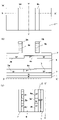
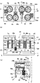
- FIG. 4 shows a schematic structural diagram of the N-channel SGT.
- Si column the silicon semiconductor column having a P-type or i-type (intrinsic type) conductive type, when one is the source, the other is the drain.
- N + layers 121a and 121b are formed (“N + layer” refers to a semiconductor region containing a high concentration of donor impurities; the same applies hereinafter).
- the portion of the Si column 120 between the N + layers 121a and 121b that serve as the source and drain becomes the channel region 122.
- the gate insulating layer 123 is formed so as to surround the channel region 122.
- the gate conductor layer 124 is formed so as to surround the gate insulating layer 123.
- the SGT is composed of N + layers 121a and 121b serving as sources and drains, a channel region 122, a gate insulating layer 123, and a gate conductor layer 124. It is opened in the insulating layer 125 on the N + layer 121b, and the N + layer 121b and the source wiring metal layer S are connected to each other via the contact hole C.
- the occupied area of the SGT corresponds to the occupied area of a single source or drain N + layer of the planar MOS transistor. Therefore, the circuit chip having the SGT can realize further reduction in the chip size as compared with the circuit chip having the planar type MOS transistor.
- a contact hole C connecting the source wiring metal layer S and the N + layer 121b is formed on the Si pillar 120 in a plan view.
- the distance between the Si pillar 120 and the adjacent Si pillar becomes shorter.
- an increase in the coupling capacitance between the electrodes of the adjacent SGTs and a decrease in the yield due to a short circuit between the electrodes of the adjacent SGTs become problems.
- FIG. 5 shows a SRAM cell (Static Random Access Memory) circuit diagram using SGT.
- This SRAM cell circuit includes two inverter circuits.
- One inverter circuit is composed of a P-channel SGT_Pc1 as a load transistor and an N-channel SGT_Nc1 as a drive transistor.
- the other inverter circuit is composed of a P channel SGT_Pc2 as a load transistor and an N channel SGT_Nc2 as a drive transistor.
- the gate of P channel SGT_Pc1 and the gate of N channel SGT_Nc1 are connected.
- the drain of the P channel SGT_Pc2 and the drain of the N channel SGT_Nc2 are connected.
- the gate of P channel SGT_Pc2 and the gate of N channel SGT_Nc2 are connected.
- the drain of the P channel SGT_Pc1 and the drain of the N channel SGT_Nc1 are connected.
- the sources of the P channels SGT_Pc1 and Pc2 are connected to the power supply terminal Vdd.
- the sources of the N channels SGT_Nc1 and Nc2 are connected to the ground terminal Vss.
- Selected N channels SGT_SN1 and SN2 are arranged on both sides of the two inverter circuits.
- the gates of the selected N channels SGT_SN1 and SN2 are connected to the word line terminal WLt.
- the source and drain of the selected N channel SGT_SN1 are connected to the drain of the N channel SGT_Nc1 and the P channel SGT_Pc1 and the bit line terminal BLt.
- the source and drain of the selected N channel SGT_SN2 are connected to the drain of the N channel SGT_Nc2 and the P channel SGT_Pc2 and the inverted bit line terminal BLRt.
- the circuit having the SRAM cell is composed of two load P channels SGT_Pc1 and Pc2, two driving N channels SGT_Nc1 and Nc2, and two selection SN1 and SN2 from a total of six SGTs. It is configured (see, for example, Patent Document 2).
- this SRAM cell how to reduce the parasitic capacitance between each electrode and the connection wiring is an issue. At the same time, it is also an issue how to reduce the defects caused by the short circuit between the electrodes due to the high density of the SRAM cell.
- the method for manufacturing a columnar semiconductor memory device of the present invention is: On the substrate, a first semiconductor column that is aligned on the first line in a plan view and forms a first SGT (Surrounding Gate Transistor) standing in a vertical direction, and adjacent to the first semiconductor column, A second semiconductor column forming a second SGT and a third semiconductor column forming a third SGT that is aligned on a second line parallel to the first line in a plan view and stands vertically. And a step of forming a fourth semiconductor column that forms a fourth SGT adjacent to the third semiconductor column.
- SGT Standard Gate Transistor
- the third gate insulating layer was surrounded, and in plan view, the third gate conductor layer protruding in the direction of the first line and the fourth gate insulating layer were surrounded.
- a first contact hole is formed on the third gate conductor layer protruding from the third semiconductor column, and at the same time, a third impurity region at the bottom of the third semiconductor column and the fourth semiconductor column.
- a second contact hole is formed on the second connection region connecting the fourth impurity region at the bottom and the second gate conductor layer protruding in the second line direction in a plan view.
- a first insulating material layer made of a first pore or a low dielectric constant material layer is formed, and at the same time, the said on the second conductor layer. It comprises a step of forming a second insulating material layer composed of a second pore or a low dielectric constant material layer in the second contact hole.
- the first SGT and the fourth SGT are selection transistors of the SRAM memory cell, and the second SGT and the third SGT are load transistors of the SRAM memory cell.
- the upper end positions of the first hole and the second hole are the first gate conductor layer, the second gate conductor layer, and the third gate conductor layer. It is desirable to form it lower than the upper end position of the fourth gate conductor layer.
- the thickness of the second gate conductor layer in the region in contact with the second contact hole is set to the thickness of the second gate conductor layer surrounding the second gate insulating layer. It is desirable to form it thicker than the thickness of the gate conductor layer.
- the first gate insulating layer, the second gate insulating layer, the third gate insulating layer, and the fourth gate insulating layer are further surrounded, and the upper surface position is positioned in the vertical direction.
- the second mask material layer is connected to the second semiconductor column and partly protrudes in the second line direction, and is connected to the third semiconductor column and partly connected to the first semiconductor column.
- the film thickness of the second gate conductor layer overlapping with the second mask material layer is formed to be thicker than the film thickness of the first mask material layer
- the third The thickness of the third gate conductor layer that overlaps with the mask material layer is formed to be thicker than the film thickness of the third mask material layer.
- the columnar semiconductor memory device of the present invention is used.
- a first semiconductor column that is aligned on the first line in a plan view and forms a first SGT (Surrounding Gate Transistor) standing in a vertical direction, and adjacent to the first semiconductor column,
- a second semiconductor column forming a second SGT, a third semiconductor column arranged on a second line parallel to the first line in a plan view and standing in a vertical direction, and the third semiconductor.
- a fourth semiconductor column that forms a fourth SGT adjacent to the column, A first gate insulating layer surrounding the first semiconductor column, a second gate insulating layer surrounding the second semiconductor column, and a third gate insulating layer surrounding the third semiconductor column.
- the third gate insulating layer was surrounded, and in plan view, the third gate conductor layer protruding in the direction of the first line and the fourth gate insulating layer were surrounded.
- a first insulating material layer made of a first pore or a low dielectric constant material layer in the first contact portion on the first conductor layer, and the second on the second conductor layer.
- the first SGT and the fourth SGT are the selection transistors of the SRAM memory cell, and the second SGT and the third SGT are the load transistors of the SRAM memory cell.
- the upper end positions of the first hole and the second hole are the first gate conductor layer, the second conductor layer, the third gate conductor layer, and the above. It is characterized in that it is lower than the upper end position of the fourth gate conductor layer.
- the region in contact with the second contact hole is characterized in that the thickness of the second gate conductor layer is thicker than the thickness of the second gate conductor layer surrounding the second gate insulating layer.
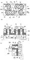
- FIGS. 1A to 1U (First Embodiment)
- a is a plan view
- (b) is a cross-sectional structure diagram along the XX'line of (a)
- (c) is a cross-sectional structure diagram along the YY'line of (a). ..
- the N layer 2 is formed on the P layer substrate 1 (which is an example of the “substrate” in the claims) by the epitaxial crystal growth method.
- N + layer 3a and P + layer (“P + layer” refers to a semiconductor region containing a high concentration of acceptor impurities; the same applies hereinafter) 4a and 4b are added to the surface layer of N layer 2 by the epitaxial crystal growth method, respectively.
- the i-layer 6 is formed.
- N + layer 3b, P + layer 4c, and 4d are formed on the i-layer 6 by the epitaxial crystal growth method.
- a mask material layer 7 composed of a SiO 2 layer, an aluminum oxide (Al 2 O 3 , hereinafter referred to as AlO) layer, and a SiO 2 layer is formed.
- AlO aluminum oxide
- SiO 2 layer silicon germanium
- the mask material layer 9 composed of the SiO 2 layer and the SiN layer is deposited.
- the i-layer 6 may be formed of N-type or P-type Si containing a small amount of donor or acceptor impurity atoms.
- the N + layer 3a, 3b, P + layer 4a, 4b, 4c, and 4d may be formed by another method such as an ion implantation method.
- the mask material layer 9 may be formed of a single layer containing a SiO 2 layer, a SiN layer, or another material layer, or a plurality of material layers.
- the mask material layer 9 is etched by the RIE (Reactive Ion Etching) method using the strip-shaped resist layer (not shown) stretched in the Y direction as a mask in the plan view formed by the lithography method. Then, using the resist layer as a mask, the mask material layer 9 is isotropically etched to form band-shaped mask material layers 9a and 9b. As a result, the widths of the band-shaped mask material layers 9a and 9b are formed to be narrower than the width of the minimum resist layer that can be formed by the lithography method. Next, using the band-shaped mask material layers 9a and 9b as masks, the SiGe layer 8 is etched by, for example, the RIE method to form the band-shaped SiGe layers 8a and 8b as shown in FIG. 1B.
- the RIE Reactive Ion Etching
- a SiN layer (not shown) is formed so as to cover the mask material layer 7, the band-shaped SiGe layers 8a and 8b, and the band-shaped mask material layers 9a and 9b by the ALD (Atomic Layered Deposition) method.
- the cross section of the SiN layer is rounded at the top. It is desirable that this roundness is formed so as to be above the band-shaped SiGe layers 8a and 8b.
- the whole is covered with, for example, a SiO 2 layer (not shown) by a flow CVD (Flow Chemical Vapor Deposition) method, and the upper surface position is a band-shaped mask material layer 9a, 9b upper surface by CMP (Chemical Mechanical Polishing).
- the SiO 2 layer and the SiN layer are polished so as to be in the position to form the SiN layers 13a, 13b and 13c. Then, the tops of the SiN layers 13a, 13b, and 13c are etched to form recesses. The bottom of the recess is formed so as to be at the lower position of the band-shaped mask material layers 9a and 9b. Then, the entire SiN layer (not shown) is coated, and the entire surface is polished by the CMP method so that the upper surface positions are the upper surface positions of the mask material layers 9a and 9b. Then, the SiO 2 layer formed by the flow CVD is removed. As a result, as shown in FIG.
- the band-shaped mask material layers 12aa, 12ab, 12ba, 12bb having the same shape as the top shape of the SiN layers 13a, 13b, 13c in a plan view on both sides of the band-shaped mask material layers 9a, 9b. Is formed.
- the strip-shaped SiN layers 13a, 13ab, 13ba are etched with the strip-shaped mask material layers 9a, 9b, 12aa, 12ab, 12ba, 12bb as masks and the SiN layers 13a, 13b, 13c are etched. , 13bb.
- the widths of the strip-shaped SiN layers 13aa, 13ab, 13ba, and 13bb are the same in a plan view.
- band-shaped mask material layers 9a and 9b and the band-shaped SiGe layers 8a and 8b are removed.
- strip-shaped mask material layers 12aa, 12ab, 12ba, and 12bb extending in the Y direction in a plan view and arranged in parallel with each other are placed on the tops of the mask material layers 7.
- the strip-shaped SiN layers 13aa, 13ab, 13ba, 13bb having the same are formed.
- the entire surface is covered to form a SiO 2 layer (not shown) by the flow CVD method.
- the SiO 2 layer is polished so that the upper surface position thereof is the same as the upper surface position of the band-shaped mask material layers 12aa, 12ab, 12ba, 12bb, and the SiO 2 layer is polished as shown in FIG. 1F.
- the SiN layer 16 is formed on the SiO 2 layer 15, the band-shaped mask material layers 12aa, 12ab, 12ba, and 12bb.
- the strip-shaped mask material layers 17a extending in the X direction on the SiN layer 16 and arranging in parallel with each other. , 17b.
- the strip-shaped mask material layers 17a and 17b are used as masks, and the SiN layer 16, the strip-shaped mask material layers 12aa, 12ab, 12ba, 12bb, the strip-shaped SiN layers 13aa, 13ab, 13ba, 13bb, and the mask.
- the material layer 7 is RIE etched.
- the remaining SiN layer 16 and SiO 2 layer 15 are removed.
- the SiN columns 20a, 20b, 20c, 20d, 20e, 20f, 20g, 20h having the rectangular mask material layers 19a, 19b, 19c, 19d, 19e, 19f, 19g, 19h at the top are formed.
- the mask material layer 19a, 19c, 19d, 19e, 19f, 19h and the SiN pillars 20a, 20c, 20d, 20e, 20f, 20h are used as masks, and the mask material layer 7 is etched and shown in FIG. 1I.
- the mask material layers 7a, 7b, 7c, 7d, 7e, and 7f are formed.
- the shapes of the mask material layers 7a, 7b, 7c, 7d, 7e, and 7f are made into a circular shape in a plan view.
- This CDE etching is not necessary when the plan view shape of the mask material layers 7a, 7b, 7c, 7d, 7e, and 7f is circular before this step. Then, the mask material layers 19a, 19c, 19d, 19e, 19f, 19h and the SiN columns 20a, 20c, 20d, 20e, 20f, 20h are removed. Then, as shown in FIG. 1I, the mask material layers 7a, 7b, 7c, 7d, 7e, and 7f are used as masks, and the N + layer 3b, P + layer 4c, 4d, and i layer 6 are etched to N +.
- Si columns 6a (an example of the "first semiconductor column” in the claims) and 6b (an example of the “second semiconductor columns” in the claims) on layers 3a, P + layers 4a and 4b. Yes), 6c, 6d, 6e (an example of the "third semiconductor pillar” in the claims), 6f (an example of the "fourth semiconductor pillar” in the claims).
- Si columns 6a, 6b, 6c are formed on the XX'line (an example of the "first line” in the claims), and the XX-XX'line (the "second line” in the claims) is formed.
- Si columns 6d, 6e, 6f are formed on the line).
- N + layer 3ba is on the top of the Si pillar 6a
- P + layer 4ca is on the top of the Si pillar 6b
- N + layer 3bb is on the top of the Si pillar 6c
- N + layer 3Ba is on the top of the Si pillar 6d (shown).
- a P + layer 4Ca (not shown) is formed on the top of the Si pillar 6e
- an N + layer 3Bb (not shown) is formed on the top of the Si pillar 6f.
- N + layer 3a, P + layer 4a, N layer 2, and P layer substrate 1 connected to the bottoms of the Si columns 6a, 6b, and 6c are etched to form the upper portion of the P layer substrate 1.
- N layer 2a, N + layer 3aa (an example of the "first impurity layer” in the claims), 3ab, P + layer 4aa (an example of the "second impurity layer” in the claims).
- Si pillar base 21a There is) to form a Si pillar base 21a.
- the HfO 2 layer 23 and the TiN layer are formed by covering the whole by the ALD method.
- the TiN layers are in contact with each other between the Si columns 6b and 6c and between the Si columns 6d and 6e.
- the TiN layer 24a (the "first gate” in the claims) surrounds the HfO 2 layer 23 (an example of the "first gate insulating layer” in the claims) surrounding the outer periphery of the Si column 6a.
- An example of a “conductor layer”) is surrounded by an HfO 2 layer 23 (an example of a "second gate insulating layer” in the claims) on the outer periphery of the Si columns 6b and 6c, and a TiN layer 24b (patent claim).
- HfO 2 layer 23 an example of a "second gate insulating layer” in the claims
- TiN layer 24b pattern claim
- the entire surface is covered with a SiO 2 layer (not shown), and then the entire surface is subjected to the CMP method so that the upper surface position thereof is the upper surface position of the mask material layers 7a, 7b, 7c, 7d, 7e, 7f. Polish to.
- the SiO 2 layer (not shown) flattened by the RIE method is etched back to form the SiO 2 layer 25.
- the tops of the HfO 2 layer 23 and the TiN layers 24a, 24b, 24c, 24d are removed.
- the TiN layers 24a, 24b, 24c, and 24d serve as SGT gate conductor layers.
- This gate conductor layer is a layer that contributes to the setting of the threshold voltage of the SGT, and may be formed from a single layer or a gate conductor layer composed of a plurality of layers.
- the gate conductor material layer is formed in contact with the entire side surface between the Si columns 6b and 6c and between the Si columns 6d and 6e.
- This W layer may be another conductor material layer.
- the HfO 2 layer 23 may be formed by changing the film thickness or the material in the Si columns 6a to 6f. Further, the SiO 2 layer 25 may be formed so that the upper surface thereof is above the upper surface positions of the TiN layers 24a to 24d.
- the SiN layer 27 is formed on the SiO 2 layer 25 on the outer peripheral portion of the Si columns 6a to 6f. Then, the entire SiO 2 layer (not shown) is covered. Then, by etching the SiO 2 layer by the RIE method, the top of the exposed Si columns 6a to 6f and the side surfaces of the mask material layers 7a to 7f are exposed to the SiO 2 layer 28a having the same width in a plan view. , 28b, 28c, 28d, 28e, 28f. In this case, the SiO 2 layer 28b and the SiO 2 layer 28c are formed apart from each other. Similarly, the SiO 2 layer 28d and the SiO 2 layer 28e are formed apart from each other.
- the SiN layer 27 may be formed on at least the TiN layers 24a, 24b, 24c, and 24d, which are gate conductor layers. Further, when the SiO 2 layer 25 is formed of the SiN layer and the upper surface thereof is formed so as to be above the upper surface position of the TiN layers 24a to 24d, the SiN layer 27 may not be formed.
- AlO aluminum oxide
- the AlO layer 29 is formed by polishing so that the upper surface position of the AlO layer is the upper surface position of the mask material layers 7a to 7f by the CMP method.
- the SiO 2 layers 28a, 28b, 28c, 28d, 28e, 28f surrounding the tops of the Si columns 6a to 6f are removed, and the recesses 30a, 30b, 30c, 30d surrounding the tops of the Si columns 6a to 6f are removed. 30e and 30f are formed.
- the AlO layer 29 may be formed of a single layer or a plurality of other material layers.
- the mask material layers 7a, 7b, 7c, 7d, 7e, and 7f are removed, and the recesses 30A, 30B, 30C, and 30D are formed on the outer periphery and the upper portion of the tops of the Si columns 6a to 6f. 30E and 30F are formed.
- the order of removing the SiO 2 layers 28a, 28b, 28c, 28d, 28e, 28f and the mask material layers 7a, 7b, 7c, 7d, 7e, 7f may come first.
- the entire SiO 2 layer (not shown) is coated by the CVD method.
- the upper surface position of the SiO 2 layer is polished to the upper surface position of the AlO layer 29 by the CMP method to cover the tops of the Si columns 6a to 6f, and the recesses 30A, 30B, 30C.
- SiO 2 layers 31a, 31b (not shown) 31c, 31d, 31e (not shown), 31f are formed in 30D, 30E, 30F.
- the SiO 2 layers 31b and 31e are removed by a lithography method and a chemical etching method.
- the P + layers 32b and 32e containing acceptor impurities are formed in the recesses 30B and 30E so as to cover the tops of the Si columns 6b and 6e by the selective epitaxial crystal growth method.
- the outer circumferences of the P + layers 32b and 32e are formed so as not to be outside the outer circumferences of the recesses 30B and 30E in a plan view.
- the tops of the Si columns 6b and 6e are thinly oxidized, and then a treatment for removing the oxide film is performed to remove the damaged layer on the top surface of the Si columns 6b and 6e. And cleaning is desirable.
- the P + layer 32b, 32e may form a single crystal P + layer 32b, 32e by using a method other than the selective epitaxial crystal growth method, for example, a molecular beam crystal growth method. Further, the P + layers 32b and 32e are coated with a semiconductor layer containing acceptor impurities on the entire surface, and then polished to the upper surface position of the AlO layer 29 by the CMP method, and then the upper surface is subjected to the CDE method or chemicals. It may be formed by etching.
- the entire SiO 2 layer (not shown) is coated and polished by the CMP method so that the upper surface position of the SiO 2 layer is the same as the upper surface position of the AlO layer 29, and the P + layer 32b, A SiO 2 layer (not shown) is coated on the 32e.
- the SiO 2 layers 31a, 31c, 31d, and 31f are removed by a lithography method and chemical etching.
- the N + layers 32a, 32c, 32d, 32f containing the donor impurities are covered with the tops of the Si columns 6a, 6c, 6d, 6f by the selective epitaxial crystal growth method, and the recesses 30A, It is formed in 30C, 30D, and 30F.
- the outer circumferences of the N + layers 32a, 32c, 32d, and 32f are formed so as not to be outside the outer circumferences of the recesses 30A, 30C, 30D, and 30F in a plan view. Then, the SiO 2 layer on the P + layers 32b and 32e is removed.
- a thin Ta layer (not shown) and a W layer (not shown) are coated on the whole.
- the W layer is polished so that the upper surface position of the W layer is the upper surface position of the AlO layer 29 by the CMP method, and the W layers 33a, 33b, 33c, 33d having Ta layers on the side surfaces and the bottom surface. , 33e, 33f are formed.
- the Ta layer between the N + layers 32a, 32c, 32d, 32f, P + layers 32b, 32e and the W layers 33a, 33b, 33c, 33d, 33e, 33f is of these two layers.
- It is a buffer layer for reducing contact resistance.
- This buffer layer may be a single layer or a plurality of other material layers.
- the region including the boundary between N + layer 3aa and P + layer 4aa (which is an example of the "first connection region” in the claims) and the TiN layer 24c.
- a contact hole C1 (an example of a "first contact hole” in the claims) is formed on the contact hole C1.
- the contact hole C2 (which is an example of the "second connection region” in the claims), the TiN layer 24b, and the region including the boundary between the N + layer 3bB and the P + layer 4bb (is an example). It forms an example of a "second contact hole” in the claims).
- etch back is performed by RIE so that the upper surface position of the W layer is lower than the upper surface position of the contact holes C1 and C2, and the W layer 34a (claimed) is formed in the contact holes C1 and C2.
- a SiO2 layer is deposited on the contact holes C1 and C2 on the W layers 34a and 34b and on the AlO layer 29 by a CVD (Chemical Vapor Deposition) method.
- the SiO2 layer is polished so that the upper surface thereof becomes the upper surface of the AlO layer 29, and the holes 36a (the "first holes” in the claims) are formed on the W layers 34a and 34b. ), 36b (an example of a “second hole” in the claims), SiO2 layer 35a (an example of a "first insulating material layer” in the claims), 35b. (An example of the "second insulating material layer” in the claims) is formed.
- the upper surface positions of the W layers 34a and 34b are formed so as to be below or near the lower end positions of the gate TiN layers 24a to 24d in the vertical direction.
- another conductor layer may be used instead of the buffer Ti layer.
- another conductor material layer may be used instead of the W layers 34a and 34b.
- the conductor layer corresponding to the W layers 34a and 34b may be directly formed without using the buffer conductor layer.
- the entire surface is covered with two layers of SiO (not shown).
- SiO 2 layer 37 As shown in FIG. 1S, after forming the SiO 2 layer 37 as a whole, at least one of the W layers 33b and 33e on the Si columns 6b and 6e is used in a plan view by using a lithography method and a RIE method. It overlaps with the portion and forms a band-shaped contact hole C3 extending in the Y direction. The bottom of the strip-shaped contact hole C3 may reach the upper surface of the SiN layer 27.
- the band-shaped contact C3 is filled to form a power supply wiring metal layer Vdd in which the W layer 33b and 33e are connected.
- the power supply wiring metal layer Vdd may be formed by using a single layer or a plurality of layers of a material made of a semiconductor containing a large amount of alloys, donors or acceptor impurities as well as metals.
- a SiO 2 layer 38 having a flat upper surface is formed so as to cover the whole.
- the ground wiring metal layer Vss1 is formed via the contact hole C4 formed on the W layer 33c on the N + layer 32c.
- the ground wiring metal layer Vss2 is formed via the contact hole C5 formed on the W layer 33d on the N + layer 32d.
- a SiO 2 layer 39 having a flat upper surface is formed so as to cover the whole.
- the word wiring metal layer WL is formed through the contact holes C6 and C7 formed on the TiN layers 24a and 24d.
- the SiO 2 layer 40 having a flat upper surface is formed so as to cover the whole.
- the inverted bit output wiring metal layer RBL and the bit output wiring metal layer BL are formed via the contact holes C8 and C9 formed in the W layers 33a and 33f on the N + layers 32a and 32f.
- the SRAM cell circuit is formed on the P layer substrate 1.
- a selection transistor SGT an example of the "first SGT” in the scope of the patent claim
- a load transistor SGT the second SGT in the scope of the patent claim
- SGT drive transistor SGT
- Si column 6c a drive transistor SGT is formed on the Si column 6d
- a load transistor SGT the third in the scope of the patent claim
- Si column 6e a load transistor SGT (the third in the scope of the patent claim) is formed on the Si column 6e.
- SGT selection transistor SGT
- a load SGT is formed on the Si columns 6b and 6e
- a drive SGT is formed on the Si columns 6c and 6d
- a selection SGT is formed on the Si columns 6a and 6f.
- the SiO 2 layers 35a and 35b including the pores 36a and 36b are effectively low dielectric constant material layers.
- another low dielectric constant material layer containing or not containing the pores 36a and 36b may be used instead of the SiO 2 layers 35a and 35b.
- a SiN layer by, for example, a CVD method, a large volume of pores is formed, thereby forming an effective low dielectric constant material layer in the contact holes C1 and C2. You may.
- the holes 36a and 36b are the SiO 2 layers 35a. , 35b, the upper end positions of the holes 36a, 36b may be higher than the upper ends of the gate TiN layers 24a to 24d.
- the W layer 34a is in direct contact with the N + layer 3aa and the P + layer 4aa, but for example, on the N + layer 3aa and the P + layer 4aa between the Si columns 6a and 6b in a plan view, for example.
- a conductor layer such as a metal or a silicide layer may be provided, and the contact hole C1 may be formed on the conductor layer. This also applies to the contact hole C2.
- the P layer substrate 1 is used as the substrate.
- the N layer 2 on the P layer substrate 1 may also include the substrate as a part.
- another substrate such as, for example, SOI (Silicon Oxide Insulator) may be used.
- the N + layer 3aa, 3ab, 3aB, 3bB, P + layer 4aa, 4bb may be formed by connecting to the bottom side surface of the Si columns 6a to 6f.
- the N + layer 3aa, 3ab, 3aB, 3bB, P + layer 4aa, 4bb, 4ca, and 4Ca serving as the source or drain of the SGT are inside the bottom or top of the Si columns 6a to 6f, or. It may be in contact with the outside of the side surface and may be formed on the outer periphery thereof, and each may be electrically connected by another conductor material.
- (Feature 1) The W layer 34a connecting the N + layer 3aa, the P + layer 4aa, and the gate TiN layer 24c between the Si columns 6a and 6b on which the selective SGT and the load SGT are formed, as shown in FIG. 1U, and an effective low dielectric.
- the SiO 2 layer 35a which is a rate layer, is formed in the contact hole C1.
- the W layer 24a and the SiO2 layer 24a are formed by self-alignment.
- the W layer 24b and the SiO2 layer 24b are formed by self-alignment. This self-alignment formation leads to high integration of SRAM cells.
- the SiO 2 layer 35a including the holes 36a reduces the coupling capacitance between the gate TiN layer 24a of the selected SGT and the gate TiN layer 24b of the load SGT and the drive SGT.
- the SiO 2 layer 35b including the pores 36b reduces the coupling capacitance between the gate TiN layer 24d of the selective SGT and the gate TiN layer 24c of the load SGT. This reduction in coupling capacity leads to higher speed and lower power consumption of the SRAM device.
- the W layer 34a is formed so that the upper surface thereof is below or near the lower end positions of the gate TiN layers 24a to 24d in the vertical direction.
- the side surface of the W layer 34a can be formed with a small area facing the side surface of the gate TiN layers 24a and 24b, or separated from the side surface.
- short-circuit defects between the W layer 34b and the gate TiN layers 24c and 24d can be reduced. This contributes to the improvement of the yield of the SRAM device.
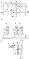
- FIGS. 2A and 2B (Second Embodiment) Hereinafter, a method for manufacturing an SRAM cell circuit having an SGT according to a second embodiment of the present invention will be described with reference to FIGS. 2A and 2B.
- (A) is a plan view
- (b) is a cross-sectional structure diagram along the XX'line of (a)
- (c) is a cross-sectional structure diagram along the YY'line of (a).
- the steps from FIG. 1A to FIG. 1R described in the first embodiment are performed.
- the entire surface is covered with a resist layer (not shown).
- the SiN layer 41, the mask material layers 7a to 7f, and the SiO 2 layers 28a to 28f are overlapped with the Si columns 6b and 6e in a plan view and have a strip shape.
- the vacant resist layer 42 is formed.
- the SiN layer 41, the mask material layers 7b, 7e, and the SiO 2 layers 28b, 28e, 35a, and 35b are placed above the top surface positions of the Si columns 6b, 6e.
- the recess 43 is formed by etching by the RIE method so as to be. In a plan view, the recess 43 partially overlaps with the SiO 2 layers 35a and 35b. The bottom of the recess 43 may reach the SiN layer 27. Further, as the resist layer 42, a single layer or another material layer composed of a plurality of layers may be used as long as it serves as an etching mask.
- the resist layer 42 is removed.
- the mask material layers 7b and 7e on the Si columns 6b and 6e and the SiO 2 layers 28b and 28e are removed.
- a thin single crystal Si layer (not shown) by the ALD method and a P + layer (not shown) containing acceptor impurities by the epitaxial crystal growth method are coated on the whole.
- the P + layer and the thin Si layer are polished so that the upper surface position thereof is the upper surface position of the SiN layer 41, and the thin single crystal Si layer 45b and the P + layer 46b are formed into the P + layer as shown in FIG. 2B. It is formed on 4ca and 4Ca.
- N + layers 46a, 46c, 46d, 46f are formed on N + layers 3ba, 3bb, 3Ba, and 3Bb. Then, the upper surface of the P + layer 46b, 46e, N + layer 46a, 46c, 46d, 46f is etched so as to be lower than the upper surface of the SiN layer 41. Then, the W layers 49a, 49b, 49c, 49d, 49e are formed on the P + layers 46b, 46e, N + layers 46a, 46c, 46d, 46f. Here, the upper end positions of the holes 36a and 36b in the vertical direction are formed so as to be below the SiN layer 27. Next, by performing the process shown in FIG. 1T, the SRAM cell circuit is formed on the P layer substrate 1.
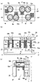
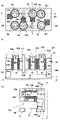
- FIGS. 3A to 3C are plan views
- (b) is a cross-sectional structure diagram along the XX'line of (a)
- (c) is a cross-sectional structure diagram along the YY'line of (a).
- the steps up to FIG. 1I in the first embodiment are performed. Then, the entire surface is covered, an HfO 2 layer (not shown) and a TiN layer (not shown) are deposited using ALD (Atomic Layered Deposition), and a SiO 2 layer (not shown) is formed by the CVD method. accumulate. Then, by the CMP method, the upper surfaces of the HfO 2 layer, the TiN layer, and the SiO 2 layer are polished so as to be at the upper surface positions of the mask material layers 7a to 7f.
- ALD Advanced Layered Deposition
- the TiN layer and the SiO2 layer are etched by the RIE method to the vicinity of the lower end position of the N + layer 3ba, 3bb, 3Ba, 3Bb, P + layer 3bb, 3Ca.
- the TiN layer 24 and the SiO2 layer 25A are formed.
- a SiN layer (not shown) is deposited on the entire surface.
- the SiN layer 26b is formed by being connected between the P + layer 4ca and the N + layer 3bb.
- the SiN layer 26c is formed by connecting the P + layer 4ca and the N + layer 3Ba.
- the mask material layer 26A partially overlapped with the SiN layer 26a
- the mask material layer 26B partially overlapped with the SiN layer 26b
- the mask material layer 26C partially overlapped with the SiN layer 26c
- the SiN layer 26d A partially overlapping mask material layer 26D is formed.
- the thickness L1 of the mask material layers 26a to 26f in a plan view is made smaller than the thickness L2 of the TiN layer.
- the SiO 2 layer 25A and the TiN layer 24 are etched by using the mask material layers 7a to 7d and 26A to 26D and the SiN layers 26a to 26d as masks, and the TiN layers 24A and 24B are etched. , 24C, 24D.
- the SiO2 layer 25A below the mask material layers 26A to 26D is left.
- the thickness of the TiN layers 24A to 24D surrounding the Si columns 6a to 6f is formed as thin as L1 while the thickness L2 of the bottom of the TiN layers 24A to 24D is maintained.
- SiO 2 layers 35a and 35b including the holes 36a and 36b are formed on the W layers 34a and 34b.
- the W layers 34a and 34b are formed on the bottom of the contact holes C1 and C2 (see FIG. 1Q).
- the contact holes C1 and C2 are formed on the thick TiN layers 24B and 24C having a thickness of L2.
- the SRAM cell is formed on the P layer substrate 1.
- the thickness of the gate TiN layers 24A to 24D may be about 2 to 5 nm as long as a predetermined work function can be obtained.
- the thinner the gate TiN layers 24A to 24D the better.
- the contact holes C1 and C2 may penetrate the TiN layers 24B and 24C when the contact holes C1 and C2 are formed. In this case, there is a high possibility that poor connection between the TiN layers 24B and 24C and the W layers 34a and 34b will occur.
- the thickness of the TiN layers 24A to 24D on the outer peripheral portion of the Si columns 6a to 6f is reduced to the thickness of the TiN layers 24B and 24C in the portions in contact with the contact holes C1 and C2. It can be thickened. This makes it possible to prevent poor connection between the TiN layers 24B and 24C and the W layers 34a and 34b.
- a logic circuit is formed around the SRAM cell region. In this logic circuit, a plurality of SGTs are connected by conductor electrodes. As the conductor electrode, a TiN layer having the same thickness as the thick TiN layers 24B and 24C connected to the W layers 34a and 34b is used.
- the TiN layer is required to have low resistance. From this point of view, it is necessary to increase the thickness of the TiN layer. On the other hand, even in the SGT in the logic circuit region, it is desirable that the gate TiN layer in the portion surrounding the Si column is thin for high integration. On the other hand, this embodiment contributes to high integration and high performance even in the SGT in the logic circuit region.
- one SGT is formed on one semiconductor column, but the present invention can also be applied to the formation of a circuit in which two or more SGTs are formed.
- the present invention can be applied to the connection between the top impurity layers of the SGT at the top of two semiconductor columns forming two or more SGTs.
- the Si columns 6a to 6f are formed in the first embodiment, the semiconductor columns may be made of other semiconductor materials. This also applies to the other embodiments according to the present invention.
- an SRAM cell composed of 6 SGTs has been described as an example.
- the present invention can be applied as long as the region where the contact hole C1 is formed between the Si columns 6a and 6b and the contact hole C2 is formed between the Si columns 6e and 6f is included. This also applies to the other embodiments according to the present invention.
- the N + layer 32a, 32c, 32d, 32f, P + layer 32b, 32e in the first embodiment may be formed of a donor, Si containing acceptor impurities, or another semiconductor material layer. Further, the N + layers 32a, 32c, 32d, 32f and the P + layers 32b, 32e may be formed from different semiconductor material layers. This also applies to the other embodiments according to the present invention.
- the AlO layer 29 surrounding the SiO 2 layers 28a to 28f another material layer including an organic material or an inorganic material composed of a single layer or a plurality of layers may be used as long as it is a material suitable for the object of the present invention. .. This also applies to the other embodiments according to the present invention.
- the mask material layer 7 is formed of a SiO 2 layer, an AlO layer, and a SiO 2 layer.
- any other material layer including an organic material or an inorganic material composed of a single layer or a plurality of layers may be used as long as it is a material suitable for the object of the present invention. This also applies to the other embodiments according to the present invention.
- strip-shaped SiN layers 13aa, 13ab, 13ba, and 13bb formed by the ALD method were formed on both sides of the strip-shaped SiGe layers 8a and 8b.
- the band-shaped SiN layers 13aa, 13ab, 13ba, 13bb and the band-shaped SiGe layers 8a, 8b are other material layers including an organic material or an inorganic material consisting of a single layer or a plurality of layers as long as they are materials suitable for the object of the present invention. May be used. This also applies to the other embodiments according to the present invention.
- N + layers 3aa, 3ab, 3ba, 3bb, P + layers 4aa, 4bb which are sources or drains of SGT, are N in the lower part of the Si columns 6a to 6f. They were connected and formed on layers 2a and 2b.
- N + layers 3aa, 3ab, 3ba, 3bb, P + layers 4aa, 4bb are formed on the bottoms of Si columns 6a to 6f
- N + layers 3aa, 3ab, 3ba, 3bb, P + layers. 4aa and 4bb may be connected via a metal layer and an alloy layer.
- the N + layer 3aa, 3ab, 3ba, 3bb, P + layer 4aa, 4bb may be formed by connecting to the bottom side surface of the Si columns 6a to 6f.
- the N + layer 3aa, 3ab, 3ba, 3bb, P + layer 4aa, 4bb which is the source or drain of the SGT, is in contact with the inside of the bottom of the Si columns 6a to 6f or the outside of the side surface thereof. It may be formed on the outer circumference, and each may be electrically connected by another conductor material. This also applies to the other embodiments according to the present invention.
- the materials of the various wiring metal layers 34a, 34b, WL, Vdd, Vss, BL, and RBL in the first embodiment are not only metals but also conductive such as a semiconductor layer containing a large amount of alloys, acceptors, or donor impurities. It may be a material layer, and may be composed of a single layer or a combination of a plurality of layers. This also applies to the other embodiments according to the present invention.
- the thin single crystal Si layers 45a to 45e are layers for forming P + layers 46b, N + layers 48a, 48b, 48c, and 48d having good crystallinity. It may be another single crystal semiconductor thin film layer.
- the shapes of the Si columns 6a to 6f in a plan view were circular.
- the shape of a part or all of the Si columns 6a to 6f in a plan view may be a circle, an ellipse, a shape elongated in one direction, or the like.
- Si columns having different planar views can be mixedly formed in the logic circuit region according to the logic circuit design. This also applies to the other embodiments of the present invention.
- N + layers 3aa, 3ab, 3aB, 3bB, P + layers 4aa and 4bb were formed by connecting to the bottoms of the Si columns 6a to 6f.
- An alloy layer such as metal or silicide may be formed on the upper surface of N + layer 3aa, 3ab, 33aB, 3bB, P + layer 4aa, 4bb.
- a donor or a P + layer or an N + layer containing acceptor impurity atoms formed by, for example, an epitaxial crystal growth method is formed on the outer periphery of the bottom of the Si columns 6a to 6f to form an SGT source or drain impurity region. It may be formed.
- the N + layer or the P + layer may or may not be formed inside the Si column in contact with the N + layer or the P + layer formed by the epitaxial crystal growth method.
- a metal layer or an alloy layer that is in contact with and stretched in contact with these P + layers and N + layers may be provided. This also applies to the other embodiments according to the present invention.
- the SGT is formed on the P layer substrate 1, but an SOI (Silicon On Insulator) substrate may be used instead of the P layer substrate 1.
- SOI Silicon On Insulator
- another material substrate may be used as long as it serves as a substrate. This also applies to the other embodiments according to the present invention.
- the SGT constituting the source and the drain by using the N + layer and the P + layer having the same polarity of conductivity above and below the Si columns 6a to 6f has been described, but the polarities are different.
- the present invention can also be applied to a tunnel type SGT having a source and a drain. This also applies to the other embodiments according to the present invention.
- thin single crystal Si layers 45a to 45e by the ALD method, and N + layers and P + layers 46a to 46e containing acceptor impurities by the epitaxial crystal growth method were formed.
- the thin single crystal Si layers 45a to 45e are material layers for obtaining N + layers and P + layers 46a to 46e having good crystallinity. As long as it is a material layer for obtaining N + layer and P + layer 46a to 46e having good crystallinity, it may be another single layer or a plurality of material layers.
- the mask material layers 7a, 7b, 7c, 7d, 7e, and 7f may not be present.
- the upper surface position of the top of the Si pillars 6a to 6f is formed by etching the tops of the Si pillars 6a to 6f or oxidizing the tops of the Si pillars 6a to 6f and then removing them. Can be lower than that of the AlO layer 29.
- the present invention allows various embodiments and modifications without departing from the broad spirit and scope of the present invention. Further, the above-described embodiment is for explaining an embodiment of the present invention, and does not limit the scope of the present invention. The above-mentioned embodiment and modification can be arbitrarily combined. Further, even if a part of the constituent requirements of the above embodiment is removed as necessary, it is within the scope of the technical idea of the present invention.
- a high-density columnar semiconductor memory device can be obtained.
Landscapes
- Engineering & Computer Science (AREA)
- Microelectronics & Electronic Packaging (AREA)
- Power Engineering (AREA)
- Physics & Mathematics (AREA)
- Ceramic Engineering (AREA)
- Condensed Matter Physics & Semiconductors (AREA)
- General Physics & Mathematics (AREA)
- Computer Hardware Design (AREA)
- Manufacturing & Machinery (AREA)
- Semiconductor Memories (AREA)
Abstract
A contact hole C1 is formed on the boundary region between an N+ layer 3aa connected to the bottom part of an Si column 6a forming a select transistor SGT on X-X' in an SRAM cell and a P+ layer 4aa connected to the bottom part of an Si column 6b forming a load transistor SGT, and a gate TiN24c surrounding an Si column 6e forming the load transistor SGT on line XX—XX'. A conductor W layer 34a is formed on the bottom part of this contact hole C1. An SiO layer 34a including a vacancy 36a is formed inside the contact hole on the W layer 34a.
Description
本発明は、柱状半導体メモリ装置とその製造方法に関する。
The present invention relates to a columnar semiconductor memory device and a method for manufacturing the same.
近年、LSI(Large Scale Integration)に3次元構造トランジスタが使われている。その中で、柱状半導体装置であるSGT(Surrounding Gate Transistor)は、高集積な半導体装置を提供する半導体素子として注目されている。また、SGTを有する半導体装置の更なる高集積化、高性能化が求められている。
In recent years, three-dimensional structure transistors have been used for LSI (Large Scale Integration). Among them, SGT (Surrounding Gate Transistor), which is a columnar semiconductor device, is attracting attention as a semiconductor element that provides a highly integrated semiconductor device. Further, there is a demand for higher integration and higher performance of semiconductor devices having SGT.
通常のプレナー型MOSトランジスタでは、チャネルが半導体基板の上表面に沿う水平方向に延在する。これに対して、SGTのチャネルは、半導体基板の上表面に対して垂直方向に延在する(例えば、特許文献1、非特許文献1を参照)。このため、SGTはプレナー型MOSトランジスタと比べ、半導体装置の高密度化が可能である。
In a normal planar MOS transistor, the channel extends horizontally along the upper surface of the semiconductor substrate. On the other hand, the channel of SGT extends in the direction perpendicular to the upper surface of the semiconductor substrate (see, for example, Patent Document 1 and Non-Patent Document 1). Therefore, the SGT can increase the density of the semiconductor device as compared with the planar type MOS transistor.
図4に、NチャネルSGTの模式構造図を示す。P型又はi型(真性型)の導電型を有するSi柱120(以下、シリコン半導体柱を「Si柱」と称する。)内の上下の位置に、一方がソースとなる場合に、他方がドレインとなるN+層121a、121bが形成されている(「N+層」は、ドナー不純物を高濃度で含む半導体領域を指す。以下同様。)。このソース、ドレインとなるN+層121a、121b間のSi柱120の部分がチャネル領域122となる。このチャネル領域122を囲むようにゲート絶縁層123が形成されている。このゲート絶縁層123を囲むようにゲート導体層124が形成されている。SGTは、ソース、ドレインとなるN+層121a、121b、チャネル領域122、ゲート絶縁層123、ゲート導体層124より構成されている。N+層121b上の絶縁層125に開けられコンタクトホールCを介してN+層121bとソース配線金属層Sが接続されている。これにより、平面視において、SGTの占有面積は、プレナー型MOSトランジスタの単一のソース又はドレインN+層の占有面積に相当する。そのため、SGTを有する回路チップは、プレナー型MOSトランジスタを有する回路チップと比較して、更なるチップサイズの縮小化が実現できる。
FIG. 4 shows a schematic structural diagram of the N-channel SGT. At the upper and lower positions in the Si column 120 (hereinafter, the silicon semiconductor column is referred to as "Si column") having a P-type or i-type (intrinsic type) conductive type, when one is the source, the other is the drain. N + layers 121a and 121b are formed (“N + layer” refers to a semiconductor region containing a high concentration of donor impurities; the same applies hereinafter). The portion of the Si column 120 between the N + layers 121a and 121b that serve as the source and drain becomes the channel region 122. The gate insulating layer 123 is formed so as to surround the channel region 122. The gate conductor layer 124 is formed so as to surround the gate insulating layer 123. The SGT is composed of N + layers 121a and 121b serving as sources and drains, a channel region 122, a gate insulating layer 123, and a gate conductor layer 124. It is opened in the insulating layer 125 on the N + layer 121b, and the N + layer 121b and the source wiring metal layer S are connected to each other via the contact hole C. Thus, in plan view, the occupied area of the SGT corresponds to the occupied area of a single source or drain N + layer of the planar MOS transistor. Therefore, the circuit chip having the SGT can realize further reduction in the chip size as compared with the circuit chip having the planar type MOS transistor.
そして、更にチップサイズの縮小化を図る場合、克服すべき課題がある。図4に示すように、ソース配線金属層SとN+層121bを繋ぐコンタクトホールCが、平面視においてSi柱120上に形成される。チップサイズの縮小化が進むと、Si柱120と隣接するSi柱との距離が短くなる。これに伴い、隣接するSGTの電極間のカップリングキャパシタンスの増大、そして隣接するSGTの電極間ショートに伴う歩留り低下が問題になる。
Then, when further reducing the chip size, there is a problem to be overcome. As shown in FIG. 4, a contact hole C connecting the source wiring metal layer S and the N + layer 121b is formed on the Si pillar 120 in a plan view. As the chip size is reduced, the distance between the Si pillar 120 and the adjacent Si pillar becomes shorter. Along with this, an increase in the coupling capacitance between the electrodes of the adjacent SGTs and a decrease in the yield due to a short circuit between the electrodes of the adjacent SGTs become problems.
図5に、SGTを用いたSRAMセル(Static Random Access Memory)回路図を示す。本SRAMセル回路は2個のインバータ回路を含んでいる。1つのインバータ回路は負荷トランジスタとしてのPチャネルSGT_Pc1と、駆動トランジスタとしてのNチャネルSGT_Nc1と、から構成されている。もう1つのインバータ回路は負荷トランジスタとしてのPチャネルSGT_Pc2と、駆動トランジスタとしてのNチャネルSGT_Nc2と、から構成されている。PチャネルSGT_Pc1のゲートとNチャネルSGT_Nc1のゲートが接続されている。PチャネルSGT_Pc2のドレインとNチャネルSGT_Nc2のドレインが接続されている。PチャネルSGT_Pc2のゲートとNチャネルSGT_Nc2のゲートが接続されている。PチャネルSGT_Pc1のドレインとNチャネルSGT_Nc1のドレインが接続されている。
FIG. 5 shows a SRAM cell (Static Random Access Memory) circuit diagram using SGT. This SRAM cell circuit includes two inverter circuits. One inverter circuit is composed of a P-channel SGT_Pc1 as a load transistor and an N-channel SGT_Nc1 as a drive transistor. The other inverter circuit is composed of a P channel SGT_Pc2 as a load transistor and an N channel SGT_Nc2 as a drive transistor. The gate of P channel SGT_Pc1 and the gate of N channel SGT_Nc1 are connected. The drain of the P channel SGT_Pc2 and the drain of the N channel SGT_Nc2 are connected. The gate of P channel SGT_Pc2 and the gate of N channel SGT_Nc2 are connected. The drain of the P channel SGT_Pc1 and the drain of the N channel SGT_Nc1 are connected.
図5に示すように、PチャネルSGT_Pc1、Pc2のソースは電源端子Vddに接続されている。そして、NチャネルSGT_Nc1、Nc2のソースはグランド端子Vssに接続されている。選択NチャネルSGT_SN1、SN2が2つのインバータ回路の両側に配置されている。選択NチャネルSGT_SN1、SN2のゲートはワード線端子WLtに接続されている。選択NチャネルSGT_SN1のソース、ドレインはNチャネルSGT_Nc1、PチャネルSGT_Pc1のドレインとビット線端子BLtに接続されている。選択NチャネルSGT_SN2のソース、ドレインはNチャネルSGT_Nc2、PチャネルSGT_Pc2のドレインと反転ビット線端子BLRtに接続されている。このようにSRAMセルを有する回路は、2個の負荷PチャネルSGT_Pc1、Pc2と、2個の駆動用NチャネルSGT_Nc1、Nc2と、2個の選択用SN1、SN2とからなる合計6個のSGTから構成されている(例えば、特許文献2を参照)。このSRAMセルにおいて、各電極間、接続配線間の寄生容量を如何に減少させるかが課題である。同時に、SRAMセルの高密度化に伴う、各電極間の短絡に伴う不良を如何に減少させるかも課題である。
As shown in FIG. 5, the sources of the P channels SGT_Pc1 and Pc2 are connected to the power supply terminal Vdd. The sources of the N channels SGT_Nc1 and Nc2 are connected to the ground terminal Vss. Selected N channels SGT_SN1 and SN2 are arranged on both sides of the two inverter circuits. The gates of the selected N channels SGT_SN1 and SN2 are connected to the word line terminal WLt. The source and drain of the selected N channel SGT_SN1 are connected to the drain of the N channel SGT_Nc1 and the P channel SGT_Pc1 and the bit line terminal BLt. The source and drain of the selected N channel SGT_SN2 are connected to the drain of the N channel SGT_Nc2 and the P channel SGT_Pc2 and the inverted bit line terminal BLRt. As described above, the circuit having the SRAM cell is composed of two load P channels SGT_Pc1 and Pc2, two driving N channels SGT_Nc1 and Nc2, and two selection SN1 and SN2 from a total of six SGTs. It is configured (see, for example, Patent Document 2). In this SRAM cell, how to reduce the parasitic capacitance between each electrode and the connection wiring is an issue. At the same time, it is also an issue how to reduce the defects caused by the short circuit between the electrodes due to the high density of the SRAM cell.
SGTを用いたSRAM回路の高性能化と、高集積化と、が求められている。
High performance and high integration of SRAM circuits using SGT are required.
上記の課題を解決するために、本発明の柱状半導体メモリ装置の製造方法は、
基板上に、平面視において第1の線上に並び、且つ垂直方向に立った第1のSGT(Surrounding Gate Transistor)を形成する第1の半導体柱と、前記第1の半導体柱に隣接して、第2のSGTを形成する第2の半導体柱と、平面視において前記第1の線に並行な第2の線上に並び、且つ垂直方向に立った第3のSGTを形成する第3の半導体柱と、前記第3の半導体柱に隣接して第4のSGTを形成する第4の半導体柱と、を形成する工程と、
前記第1の半導体柱を囲んだ第1のゲート絶縁層と、前記第2の半導体柱を囲んだ第2のゲート絶縁層と、前記第3の半導体柱を囲んだ第3のゲート絶縁層と、前記第4の半導体柱を囲んだ第4のゲート絶縁層と、を形成する工程と、
前記第1のゲート絶縁層を囲んだ第1のゲート導体層と、前記第2のゲート絶縁層を囲み、且つ、平面視において、前記第2の線の方向に突き出た第2のゲート導体層と、平面視において、前記第3のゲート絶縁層を囲み、且つ、平面視において、前記第1の線の方向に突き出た第3のゲート導体層と、前記第4のゲート絶縁層を囲んだ第4のゲート導体層と、を形成する工程と、
前記第1の半導体柱の底部にある第1の不純物領域と、前記第2の半導体柱の底部にある第2の不純物領域とを繋げる第1の接続領域と、平面視において第1の線方向に突き出た前記第3のゲート導体層と、の上に第1のコンタクトホールを形成し、同時に、前記第3の半導体柱の底部にある第3の不純物領域と、前記第4の半導体柱の底部にある第4の不純物領域とを繋げる第2の接続領域と、平面視において前記第2の線方向に突き出た前記第2のゲート導体層と、の上に第2のコンタクトホールを形成する工程と、
前記第1のコンタクトホールの底部に第1の導体層を形成し、同時に前記第2のコンタクトホールの底部に第2の導体層を形成する工程と、
前記第1の導体層上の前記第1のコンタクトホール内に、第1の空孔または低誘電率材料層よりなる第1の絶縁材料層を形成し、同時に前記第2の導体層上の前記第2のコンタクトホール内に、第2の空孔または低誘電率材料層よりなる第2の絶縁材料層を形成する工程と、を有し、
前記第1のSGTと、前記第4のSGTがSRAMメモリセルの選択トランジスタであり、前記第2のSGTと、前記第3のSGTがSRAMメモリセルの負荷トランジスタであることを特徴とする。 In order to solve the above problems, the method for manufacturing a columnar semiconductor memory device of the present invention is:
On the substrate, a first semiconductor column that is aligned on the first line in a plan view and forms a first SGT (Surrounding Gate Transistor) standing in a vertical direction, and adjacent to the first semiconductor column, A second semiconductor column forming a second SGT and a third semiconductor column forming a third SGT that is aligned on a second line parallel to the first line in a plan view and stands vertically. And a step of forming a fourth semiconductor column that forms a fourth SGT adjacent to the third semiconductor column.
A first gate insulating layer surrounding the first semiconductor column, a second gate insulating layer surrounding the second semiconductor column, and a third gate insulating layer surrounding the third semiconductor column. , The step of forming the fourth gate insulating layer surrounding the fourth semiconductor column, and
A first gate conductor layer surrounding the first gate insulating layer and a second gate conductor layer surrounding the second gate insulating layer and protruding in the direction of the second line in a plan view. In plan view, the third gate insulating layer was surrounded, and in plan view, the third gate conductor layer protruding in the direction of the first line and the fourth gate insulating layer were surrounded. The process of forming the fourth gate conductor layer, and
A first connection region connecting a first impurity region at the bottom of the first semiconductor column and a second impurity region at the bottom of the second semiconductor column, and a first line direction in a plan view. A first contact hole is formed on the third gate conductor layer protruding from the third semiconductor column, and at the same time, a third impurity region at the bottom of the third semiconductor column and the fourth semiconductor column. A second contact hole is formed on the second connection region connecting the fourth impurity region at the bottom and the second gate conductor layer protruding in the second line direction in a plan view. Process and
A step of forming a first conductor layer at the bottom of the first contact hole and at the same time forming a second conductor layer at the bottom of the second contact hole.
In the first contact hole on the first conductor layer, a first insulating material layer made of a first pore or a low dielectric constant material layer is formed, and at the same time, the said on the second conductor layer. It comprises a step of forming a second insulating material layer composed of a second pore or a low dielectric constant material layer in the second contact hole.
The first SGT and the fourth SGT are selection transistors of the SRAM memory cell, and the second SGT and the third SGT are load transistors of the SRAM memory cell.
上記発明において、垂直方向において、前記第1の空孔、前記第2の空孔の上端位置が、前記第1のゲート導体層、前記第2のゲート導体層、前記第3のゲート導体層、前記第4のゲート導体層の上端位置より低く形成する、ことが望ましい。
In the above invention, in the vertical direction, the upper end positions of the first hole and the second hole are the first gate conductor layer, the second gate conductor layer, and the third gate conductor layer. It is desirable to form it lower than the upper end position of the fourth gate conductor layer.
前記第2のゲート導体層を形成する工程において、前記第2のコンタクトホールに接する領域の、前記第2のゲート導体層の厚さを、前記第2のゲート絶縁層を囲んだ前記第2のゲート導体層の厚さより厚く形成することが望ましい。
In the step of forming the second gate conductor layer, the thickness of the second gate conductor layer in the region in contact with the second contact hole is set to the thickness of the second gate conductor layer surrounding the second gate insulating layer. It is desirable to form it thicker than the thickness of the gate conductor layer.
上記発明において、さらに、前記第1のゲート絶縁層、前記第2のゲート絶縁層、前記第3のゲート絶縁層、前記第4のゲート絶縁層、を囲み、且つ、垂直方向において、上面位置が前記第1の半導体柱、前記第2の半導体柱、前記第3の半導体柱、前記第4の半導体柱の頂部より下にある第2の導体層を形成する工程と、
前記第1の半導体柱、前記第2の半導体柱、前記第3の半導体柱、前記第4の半導体柱の頂部を囲んだ第1のマスク材料層を形成する工程と、
平面視において、前記第2の半導体柱に繋がり、且つ一部が前記第2の線方向に突き出た第2のマスク材料層と、前記第3の半導体柱に繋がり、且つ一部が前記第1の線方向に突き出た第3のマスク材料層と、を形成する工程と、
前記第1のマスク材料層と、前記第2のマスク材料層と、前記第3のマスク材料層と、をマスクにして、前記第2の導体層をエッチングして、前記第1のゲート導体層、前記第2のゲート導体層、前記第3のゲート導体層、前記第4のゲート導体層を形成する工程と、有し、
平面視において、前記第2のマスク材料層と重なった、前記第2のゲート導体層の膜厚が、前記第1のマスク材料層の膜厚より厚く形成され、平面視において、前記第3のマスク材料層と重なった、前記第3のゲート導体層の膜厚が、前記第3のマスク材料層の膜厚より厚く形成する。 In the above invention, the first gate insulating layer, the second gate insulating layer, the third gate insulating layer, and the fourth gate insulating layer are further surrounded, and the upper surface position is positioned in the vertical direction. A step of forming a second conductor layer below the top of the first semiconductor column, the second semiconductor column, the third semiconductor column, and the fourth semiconductor column.
A step of forming a first mask material layer surrounding the first semiconductor column, the second semiconductor column, the third semiconductor column, and the top of the fourth semiconductor column.
In a plan view, the second mask material layer is connected to the second semiconductor column and partly protrudes in the second line direction, and is connected to the third semiconductor column and partly connected to the first semiconductor column. A process of forming a third mask material layer protruding in the line direction of
Using the first mask material layer, the second mask material layer, and the third mask material layer as masks, the second conductor layer is etched to obtain the first gate conductor layer. The step of forming the second gate conductor layer, the third gate conductor layer, and the fourth gate conductor layer.
In the plan view, the film thickness of the second gate conductor layer overlapping with the second mask material layer is formed to be thicker than the film thickness of the first mask material layer, and in the plan view, the third The thickness of the third gate conductor layer that overlaps with the mask material layer is formed to be thicker than the film thickness of the third mask material layer.
上記の課題を解決するために、本発明の柱状半導体メモリ装置は、
基板上に、平面視において第1の線上に並び、且つ垂直方向に立った第1のSGT(Surrounding Gate Transistor)を形成する第1の半導体柱と、前記第1の半導体柱に隣接して、第2のSGTを形成する第2の半導体柱と、平面視において前記第1の線に並行な第2の線上に並び、且つ垂直方向に立った第3の半導体柱と、前記第3の半導体柱に隣接して第4のSGTを形成する第4の半導体柱と、
前記第1の半導体柱を囲んだ第1のゲート絶縁層と、前記第2の半導体柱を囲んだ第2のゲート絶縁層と、前記第3の半導体柱を囲んだ第3のゲート絶縁層と、前記第4の半導体柱を囲んだ第4のゲート絶縁層と、
前記第1のゲート絶縁層を囲んだ第1のゲート導体層と、前記第2のゲート絶縁層を囲み、且つ、平面視において、前記第2の線の方向に突き出た第2のゲート導体層と、平面視において、前記第3のゲート絶縁層を囲み、且つ、平面視において、前記第1の線の方向に突き出た第3のゲート導体層と、前記第4のゲート絶縁層を囲んだ第4のゲート導体層と、
前記第1の半導体柱の底部にある第1の不純物領域と、前記第2の半導体柱の底部にある第2の不純物領域とを繋げる第1の接続領域と、平面視において第1の線方向に突き出た前記第3のゲート導体層と、の上に垂直方向に延びた第1のコンタクト部と、前記第3の半導体柱の底部にある第3の不純物領域と、前記第4の半導体柱の底部にある第4の不純物領域とを繋げる第2の接続領域と、平面視において前記第2の線方向に突き出た前記第2のゲート導体層と、の上に垂直方向に延びた第2のコンタクト部と、
前記第1のコンタクト部の底部にある第1の導体層と、前記第2のコンタクト部の底部にある第2の導体層と、
前記第1の導体層上の前記第1のコンタクト部内にある、第1の空孔、または低誘電率材料層よりなる第1の絶縁材料層と、前記第2の導体層上の前記第2のコンタクト部内にある、第2の空孔、または低誘電率材料層よりなる第2の絶縁材料層と、を有し、
前記第1のSGTと、前記4のSGTがSRAMメモリセルの選択トランジスタであり、前記第2のSGTと、前記第3のSGTがSRAMメモリセルの負荷トランジスタであることを特徴とする。 In order to solve the above problems, the columnar semiconductor memory device of the present invention is used.
On the substrate, a first semiconductor column that is aligned on the first line in a plan view and forms a first SGT (Surrounding Gate Transistor) standing in a vertical direction, and adjacent to the first semiconductor column, A second semiconductor column forming a second SGT, a third semiconductor column arranged on a second line parallel to the first line in a plan view and standing in a vertical direction, and the third semiconductor. A fourth semiconductor column that forms a fourth SGT adjacent to the column,
A first gate insulating layer surrounding the first semiconductor column, a second gate insulating layer surrounding the second semiconductor column, and a third gate insulating layer surrounding the third semiconductor column. , The fourth gate insulating layer surrounding the fourth semiconductor column, and
A first gate conductor layer surrounding the first gate insulating layer and a second gate conductor layer surrounding the second gate insulating layer and protruding in the direction of the second line in a plan view. In plan view, the third gate insulating layer was surrounded, and in plan view, the third gate conductor layer protruding in the direction of the first line and the fourth gate insulating layer were surrounded. The fourth gate conductor layer and
A first connection region connecting a first impurity region at the bottom of the first semiconductor column and a second impurity region at the bottom of the second semiconductor column, and a first line direction in a plan view. A third gate conductor layer protruding from the surface, a first contact portion extending vertically above the third gate conductor layer, a third impurity region at the bottom of the third semiconductor column, and the fourth semiconductor column. A second extending vertically over a second connecting region connecting the fourth impurity region at the bottom of the surface and the second gate conductor layer projecting in the second line direction in a plan view. Contact part and
A first conductor layer at the bottom of the first contact portion and a second conductor layer at the bottom of the second contact portion.
A first insulating material layer made of a first pore or a low dielectric constant material layer in the first contact portion on the first conductor layer, and the second on the second conductor layer. It has a second pore, or a second insulating material layer made of a low dielectric constant material layer, in the contact portion of the above.
The first SGT and the fourth SGT are the selection transistors of the SRAM memory cell, and the second SGT and the third SGT are the load transistors of the SRAM memory cell.
上記発明において、垂直方向において、前記第1の空孔、前記第2の空孔の上端位置が、前記第1のゲート導体層、前記第2の導体層、前記第3のゲート導体層、前記第4のゲート導体層の上端位置より低いことを特徴とする。
In the above invention, in the vertical direction, the upper end positions of the first hole and the second hole are the first gate conductor layer, the second conductor layer, the third gate conductor layer, and the above. It is characterized in that it is lower than the upper end position of the fourth gate conductor layer.
前記第2のコンタクトホールに接する領域の、前記第2のゲート導体層の厚さが、前記第2のゲート絶縁層を囲んだ前記第2のゲート導体層の厚さより厚いことを特徴とする。
The region in contact with the second contact hole is characterized in that the thickness of the second gate conductor layer is thicker than the thickness of the second gate conductor layer surrounding the second gate insulating layer.
以下、本発明の実施形態に係る、柱状半導体メモリ装置の製造方法について、図面を参照しながら説明する。
Hereinafter, a method for manufacturing a columnar semiconductor memory device according to an embodiment of the present invention will be described with reference to the drawings.
(第1実施形態)
以下、図1A~図1Uを参照しながら、本発明の第1実施形態に係る、SGTを有するSRAMセル回路の製造方法について説明する。各図において、(a)は平面図、(b)は(a)のX-X’線に沿う断面構造図、(c)は(a)のY-Y’線に沿う断面構造図を示す。 (First Embodiment)
Hereinafter, a method for manufacturing an SRAM cell circuit having an SGT according to the first embodiment of the present invention will be described with reference to FIGS. 1A to 1U. In each figure, (a) is a plan view, (b) is a cross-sectional structure diagram along the XX'line of (a), and (c) is a cross-sectional structure diagram along the YY'line of (a). ..
図1Aに示すように、P層基板1(特許請求の範囲の「基板」の一例である)上にN層2をエピタキシャル結晶成長法により形成する。そして、N層2の表層にN+層3aとP+層(「P+層」は、アクセプタ不純物を高濃度で含む半導体領域を指す。以下同様。)4a、4bを、それぞれエピタキシャル結晶成長法により形成する。そして、i層6を形成する。そして、i層6上にエピタキシャル結晶成長法によりN+層3b、P+層4c、4dを形成する。そして、例えば、SiO2層、酸化アルミニウム(Al2O3、以後AlOと称する)層、SiO2層よりなるマスク材料層7を形成する。そして、シリコンゲルマニウム(SiGe)層8を堆積する。そして、SiO2層、SiN層からなるマスク材料層9を堆積する。なお、i層6はドナーまたはアクセプタ不純物原子を少量に含むN型、またはP型のSiで形成してもよい。また、N+層3a、3b、P+層4a、4b、4c、4dはイオン注入法などほかの方法で形成してもよい。また、マスク材料層9はSiO2層、SiN層を含む、または他の材料層よりなる単層、または複数の材料層より形成してよい。
As shown in FIG. 1A, the N layer 2 is formed on the P layer substrate 1 (which is an example of the “substrate” in the claims) by the epitaxial crystal growth method. Then, N + layer 3a and P + layer (“P + layer” refers to a semiconductor region containing a high concentration of acceptor impurities; the same applies hereinafter) 4a and 4b are added to the surface layer of N layer 2 by the epitaxial crystal growth method, respectively. Formed by. Then, the i-layer 6 is formed. Then, N + layer 3b, P + layer 4c, and 4d are formed on the i-layer 6 by the epitaxial crystal growth method. Then, for example, a mask material layer 7 composed of a SiO 2 layer, an aluminum oxide (Al 2 O 3 , hereinafter referred to as AlO) layer, and a SiO 2 layer is formed. Then, the silicon germanium (SiGe) layer 8 is deposited. Then, the mask material layer 9 composed of the SiO 2 layer and the SiN layer is deposited. The i-layer 6 may be formed of N-type or P-type Si containing a small amount of donor or acceptor impurity atoms. Further, the N + layer 3a, 3b, P + layer 4a, 4b, 4c, and 4d may be formed by another method such as an ion implantation method. Further, the mask material layer 9 may be formed of a single layer containing a SiO 2 layer, a SiN layer, or another material layer, or a plurality of material layers.
次に、リソグラフィ法により形成した平面視においてY方向に伸延した帯状レジスト層(図示せず)をマスクにして、マスク材料層9をRIE(Reactive Ion Etching)法によりエッチングする。そして、レジスト層をマスクにして、マスク材料層9を等方性エッチングして帯状マスク材料層9a、9bをする。これにより、帯状マスク材料層9a、9bの幅を、リソグラフィ法で形成できる最小のレジスト層の幅より細くなるように形成される。次に、帯状マスク材料層9a、9bをマスクにして、SiGe層8を、例えばRIE法によりエッチングすることにより、図1Bに示すように、帯状SiGe層8a、8bを形成する。
Next, the mask material layer 9 is etched by the RIE (Reactive Ion Etching) method using the strip-shaped resist layer (not shown) stretched in the Y direction as a mask in the plan view formed by the lithography method. Then, using the resist layer as a mask, the mask material layer 9 is isotropically etched to form band-shaped mask material layers 9a and 9b. As a result, the widths of the band-shaped mask material layers 9a and 9b are formed to be narrower than the width of the minimum resist layer that can be formed by the lithography method. Next, using the band-shaped mask material layers 9a and 9b as masks, the SiGe layer 8 is etched by, for example, the RIE method to form the band-shaped SiGe layers 8a and 8b as shown in FIG. 1B.
次に、全体に、ALD(Atomic Layered Deposition)法によりSiN層(図示せず)をマスク材料層7、帯状SiGe層8a、8b、帯状マスク材料層9a、9bを覆って形成する。この場合、SiN層の断面は頂部で丸みを生じる。この丸みは帯状SiGe層8a、8bより上部になるように形成するのが望ましい。そして、全体を、例えばフローCVD(Flow Chemical Vapor Deposition)法によるSiO2層(図示せず)で覆い、そして、CMP(Chemical Mechanical Polishing)により、上表面位置が帯状マスク材料層9a、9b上表面位置になるようにSiO2層と、SiN層と、を研磨して、SiN層13a、13b、13cを形成する。そして、SiN層13a、13b、13cの頂部をエッチングして凹部を形成する。この凹部の底部位置が、帯状マスク材料層9a、9bの下部位置にあるように形成する。そして、全体にSiN層(図示せず)を被覆し、全体をCMP法により、上面位置がマスク材料層9a、9b上面位置になるようにSiN層を研磨する。そして、フローCVDにより形成したSiO2層を除去する。これにより、図1Cに示すように、帯状マスク材料層9a、9bの両側に、平面視においてSiN層13a、13b、13cの頂部形状と同じ形状を有する帯状マスク材料層12aa、12ab、12ba、12bbが形成される。
Next, a SiN layer (not shown) is formed so as to cover the mask material layer 7, the band-shaped SiGe layers 8a and 8b, and the band-shaped mask material layers 9a and 9b by the ALD (Atomic Layered Deposition) method. In this case, the cross section of the SiN layer is rounded at the top. It is desirable that this roundness is formed so as to be above the band-shaped SiGe layers 8a and 8b. Then, the whole is covered with, for example, a SiO 2 layer (not shown) by a flow CVD (Flow Chemical Vapor Deposition) method, and the upper surface position is a band-shaped mask material layer 9a, 9b upper surface by CMP (Chemical Mechanical Polishing). The SiO 2 layer and the SiN layer are polished so as to be in the position to form the SiN layers 13a, 13b and 13c. Then, the tops of the SiN layers 13a, 13b, and 13c are etched to form recesses. The bottom of the recess is formed so as to be at the lower position of the band-shaped mask material layers 9a and 9b. Then, the entire SiN layer (not shown) is coated, and the entire surface is polished by the CMP method so that the upper surface positions are the upper surface positions of the mask material layers 9a and 9b. Then, the SiO 2 layer formed by the flow CVD is removed. As a result, as shown in FIG. 1C, the band-shaped mask material layers 12aa, 12ab, 12ba, 12bb having the same shape as the top shape of the SiN layers 13a, 13b, 13c in a plan view on both sides of the band-shaped mask material layers 9a, 9b. Is formed.
次に、図1Dに示すように、帯状マスク材料層9a、9b、12aa、12ab、12ba、12bbをマスクにして、SiN層13a、13b、13cをエッチングして、帯状SiN層13aa、13ab、13ba、13bbを形成する。この場合、平面視において、帯状SiN層13aa、13ab、13ba、13bbの幅は同じになる。
Next, as shown in FIG. 1D, the strip-shaped SiN layers 13a, 13ab, 13ba are etched with the strip-shaped mask material layers 9a, 9b, 12aa, 12ab, 12ba, 12bb as masks and the SiN layers 13a, 13b, 13c are etched. , 13bb. In this case, the widths of the strip-shaped SiN layers 13aa, 13ab, 13ba, and 13bb are the same in a plan view.
次に、帯状マスク材料層9a、9b、帯状SiGe層8a、8bを除去する。これにより、図1Eに示すように、マスク材料層7上に、平面視においてY方向に伸延し、かつ互いに平行に並んだ帯状マスク材料層12aa、12ab、12ba、12bbを、それぞれの頂部上に有する帯状SiN層13aa、13ab、13ba、13bbが形成される。
Next, the band-shaped mask material layers 9a and 9b and the band-shaped SiGe layers 8a and 8b are removed. As a result, as shown in FIG. 1E, strip-shaped mask material layers 12aa, 12ab, 12ba, and 12bb extending in the Y direction in a plan view and arranged in parallel with each other are placed on the tops of the mask material layers 7. The strip-shaped SiN layers 13aa, 13ab, 13ba, 13bb having the same are formed.
次に、全体を覆って、フローCVD法によるSiO2層(図示せず)を形成する。そして、CMP法により、SiO2層を、その上表面位置が帯状マスク材料層12aa、12ab、12ba、12bbの上表面位置と同じくなるように、研磨して、図1Fに示すように、SiO2層15を形成する。そして、SiO2層15、帯状マスク材料層12aa、12ab、12ba、12bb上に、SiN層16を形成する。そして、帯状SiN層13aa、13ab、13ba、13bbを形成した方法と、同じ基本的な手法を用いて、SiN層16上にX方向に伸延して、且つ互いに平行に並んだ帯状マスク材料層17a、17bを形成する。
Next, the entire surface is covered to form a SiO 2 layer (not shown) by the flow CVD method. Then, by the CMP method, the SiO 2 layer is polished so that the upper surface position thereof is the same as the upper surface position of the band-shaped mask material layers 12aa, 12ab, 12ba, 12bb, and the SiO 2 layer is polished as shown in FIG. 1F. Form the layer 15. Then, the SiN layer 16 is formed on the SiO 2 layer 15, the band-shaped mask material layers 12aa, 12ab, 12ba, and 12bb. Then, using the same basic method as the method of forming the strip-shaped SiN layers 13aa, 13ab, 13ba, 13bb, the strip-shaped mask material layers 17a extending in the X direction on the SiN layer 16 and arranging in parallel with each other. , 17b.
次に、図1Gに示すように、帯状マスク材料層17a、17bをマスクにして、SiN層16、帯状マスク材料層12aa、12ab、12ba、12bb、帯状SiN層13aa、13ab、13ba、13bb、マスク材料層7をRIEエッチングする。そして、残存しているSiN層16、SiO2層15を除去する。これにより、平面視において、矩形状のマスク材料層19a、19b、19c、19d、19e、19f、19g、19hを頂部に有するSiN柱20a、20b、20c、20d、20e、20f、20g、20hを形成する。
Next, as shown in FIG. 1G, the strip-shaped mask material layers 17a and 17b are used as masks, and the SiN layer 16, the strip-shaped mask material layers 12aa, 12ab, 12ba, 12bb, the strip-shaped SiN layers 13aa, 13ab, 13ba, 13bb, and the mask. The material layer 7 is RIE etched. Then, the remaining SiN layer 16 and SiO 2 layer 15 are removed. Thereby, in a plan view, the SiN columns 20a, 20b, 20c, 20d, 20e, 20f, 20g, 20h having the rectangular mask material layers 19a, 19b, 19c, 19d, 19e, 19f, 19g, 19h at the top are formed. Form.
次に、図1Hに示すように、矩形状のマスク材料層19b、19g、SiN柱20b、20gを除去する。
Next, as shown in FIG. 1H, the rectangular mask material layers 19b and 19g and the SiN columns 20b and 20g are removed.
次に、マスク材料層19a、19c、19d、19e、19f、19hと、SiN柱20a、20c、20d、20e、20f、20hをマスクにして、マスク材料層7をエッチングして、図1Iに示すように、マスク材料層7a、7b、7c、7d、7e、7fを形成する。このエッチングにおいて、例えばCDE(Chemical Dry Etching)法による等方エッチングを行うことにより、平面視において、マスク材料層7a、7b、7c、7d、7e、7fの形状を円形状にする。このCDEエッチングは、この工程の前にマスク材料層7a、7b、7c、7d、7e、7fの平面視形状が円形状になっている場合は必要ない。そして、マスク材料層19a、19c、19d、19e、19f、19hと、SiN柱20a、20c、20d、20e、20f、20hを除去する。そして、図1Iに示すように、マスク材料層7a、7b、7c、7d、7e、7fをマスクにして、N+層3b、P+層4c、4d、i層6をエッチングして、N+層3a、P+層4a、4b上にSi柱6a(特許請求の範囲の「第1の半導体柱」の一例である)、6b(特許請求の範囲の「第2の半導体柱」の一例である)、6c、6d、6e(特許請求の範囲の「第3の半導体柱」の一例である)、6f(特許請求の範囲の「第4の半導体柱」の一例である)を形成する。X-X’線(特許請求の範囲の「第1の線」の一例である)上にSi柱6a、6b、6cが形成され、XX-XX’ 線 (特許請求の範囲の「第2の線」の一例である)上にSi柱6d、6e、6fが形成される。そして、Si柱6aの頂部にN+層3baが、Si柱6bの頂部にP+層4caが、Si柱6cの頂部にN+層3bbが、Si柱6dの頂部にN+層3Ba(図示せず)が、Si柱6eの頂部にP+層4Ca(図示せず)が、Si柱6fの頂部にN+層3Bb(図示せず)が形成される。
Next, the mask material layer 19a, 19c, 19d, 19e, 19f, 19h and the SiN pillars 20a, 20c, 20d, 20e, 20f, 20h are used as masks, and the mask material layer 7 is etched and shown in FIG. 1I. As described above, the mask material layers 7a, 7b, 7c, 7d, 7e, and 7f are formed. In this etching, for example, by performing isotropic etching by a CDE (Chemical Dry Etching) method, the shapes of the mask material layers 7a, 7b, 7c, 7d, 7e, and 7f are made into a circular shape in a plan view. This CDE etching is not necessary when the plan view shape of the mask material layers 7a, 7b, 7c, 7d, 7e, and 7f is circular before this step. Then, the mask material layers 19a, 19c, 19d, 19e, 19f, 19h and the SiN columns 20a, 20c, 20d, 20e, 20f, 20h are removed. Then, as shown in FIG. 1I, the mask material layers 7a, 7b, 7c, 7d, 7e, and 7f are used as masks, and the N + layer 3b, P + layer 4c, 4d, and i layer 6 are etched to N +. Si columns 6a (an example of the "first semiconductor column" in the claims) and 6b (an example of the "second semiconductor columns" in the claims) on layers 3a, P + layers 4a and 4b. Yes), 6c, 6d, 6e (an example of the "third semiconductor pillar" in the claims), 6f (an example of the "fourth semiconductor pillar" in the claims). Si columns 6a, 6b, 6c are formed on the XX'line (an example of the "first line" in the claims), and the XX-XX'line (the "second line" in the claims) is formed. Si columns 6d, 6e, 6f are formed on the line). Then, N + layer 3ba is on the top of the Si pillar 6a, P + layer 4ca is on the top of the Si pillar 6b, N + layer 3bb is on the top of the Si pillar 6c, and N + layer 3Ba is on the top of the Si pillar 6d (shown). However, a P + layer 4Ca (not shown) is formed on the top of the Si pillar 6e, and an N + layer 3Bb (not shown) is formed on the top of the Si pillar 6f.
次に、図1Jに示すように、Si柱6a、6b、6cの底部に繋がるN+層3a、P+層4a、N層2、P層基板1をエッチングして、P層基板1の上部、N層2a、N+層3aa(特許請求の範囲の「第1の不純物層」の一例である)、3ab、P+層4aa(特許請求の範囲の「第2の不純物層」の一例である)よりなるSi柱台21aを形成する。同時に、図1J(a)のXX-XX’ 線に沿う断面構造図を示す図1J(d)に示すように、Si柱6d、6e、6fの底部に繋がるN+層3a、P+層4b、N層2、P層基板1をエッチングして、P層基板1の上部、N層2b、P+層4bb(特許請求の範囲の「第3の不純物層」の一例である)、N+層3aB、3bB(特許請求の範囲の「第4の不純物層」の一例である)、よりなるSi柱台21bを形成する。そして、N+層3aa、3ab、3aB、3bB、P+層4aa、4bb、N層2a、2bの外周部と、P層基板1上にSiO2層22を形成する。そして、ALD法により、全体を覆って、HfO2層23、TiN層(図示せず)を形成する。この場合、Si柱6b、6c間と、Si柱6d、6e間と、ではTiN層が、側面同士で接触している。そして、Si柱6aの外周を囲んだHfO2層23(特許請求の範囲の「第1のゲート絶縁層」の一例である)を囲んでTiN層24a(特許請求の範囲の「第1のゲート導体層」の一例である)を、Si柱6b、6cの外周のHfO2層23(特許請求の範囲の「第2のゲート絶縁層」の一例である)を囲んでTiN層24b(特許請求の範囲の「第2のゲート導体層」の一例である)を、Si柱6d、6eの外周のHfO2層23(特許請求の範囲の「第3のゲート絶縁層」の一例である)を囲んでTiN層24c(特許請求の範囲の「第3のゲート導体層」の一例である)を、Si柱6fの外周のHfO2層23(特許請求の範囲の「第4ゲート絶縁層」の一例である)を囲んでTiN層24d(特許請求の範囲の「第4のゲート導体層」の一例である)を形成する。そして、全体にSiO2層(図示せず)を被覆し、その後に、CMP法により全体を、その上面位置が、マスク材料層7a、7b、7c、7d、7e、7fの上面位置になるように研磨する。そして、RIE法により平坦化したSiO2層(図示せず)をエッチバックして、SiO2層25を形成する。そして、マスク材料層7a、7b、7c、7d、7e、7fと、SiO2層25と、をマスクにして、HfO2層23、TiN層24a、24b、24c、24dの頂部を除去する。TiN層24a、24b、24c、24dはSGTのゲート導体層となる。このゲート導体層は、SGTの閾値電圧の設定に寄与する層であり、単層または複数層からなるゲート導体層から形成してもよい。このゲート導体材料層は、Si柱6b、6c間、及びSi柱6d、6e間の側面全体に接して形成される。なお、TiN層24a、24b、24c、24dに繋がって、例えばタングステン(W)層を形成して、このW層を含めてゲート導体層として用いてもよい。このW層は、他の導体材料層であってもよい。また、HfO2層23は、Si柱6a~6fにおいて、膜厚または材料をかえて形成してもよい。また、SiO2層25は、その上面がTiN層24a~24dの上面位置より上になるように形成してもよい。
Next, as shown in FIG. 1J, the N + layer 3a, P + layer 4a, N layer 2, and P layer substrate 1 connected to the bottoms of the Si columns 6a, 6b, and 6c are etched to form the upper portion of the P layer substrate 1. , N layer 2a, N + layer 3aa (an example of the "first impurity layer" in the claims), 3ab, P + layer 4aa (an example of the "second impurity layer" in the claims). There is) to form a Si pillar base 21a. At the same time, as shown in FIG. 1J (d) showing the cross-sectional structure diagram along the XX-XX'line of FIG. 1J (a), N + layer 3a, P + layer 4b connected to the bottom of the Si columns 6d, 6e, 6f. , N layer 2, P layer substrate 1 is etched, and the upper part of P layer substrate 1, N layer 2b, P + layer 4bb (an example of the "third impurity layer" in the claims), N + A Si column base 21b composed of layers 3aB and 3bB (which is an example of the "fourth impurity layer" in the claims) is formed. Then, the SiO 2 layer 22 is formed on the outer peripheral portions of the N + layer 3aa, 3ab, 3aB, 3bB, P + layer 4aa, 4bb, N layer 2a, 2b, and the P layer substrate 1. Then, the HfO 2 layer 23 and the TiN layer (not shown) are formed by covering the whole by the ALD method. In this case, the TiN layers are in contact with each other between the Si columns 6b and 6c and between the Si columns 6d and 6e. Then, the TiN layer 24a (the "first gate" in the claims) surrounds the HfO 2 layer 23 (an example of the "first gate insulating layer" in the claims) surrounding the outer periphery of the Si column 6a. An example of a "conductor layer") is surrounded by an HfO 2 layer 23 (an example of a "second gate insulating layer" in the claims) on the outer periphery of the Si columns 6b and 6c, and a TiN layer 24b (patent claim). (It is an example of the " second gate conductor layer" in the range of Surrounding the TiN layer 24c (an example of the "third gate conductor layer" in the claims) is the HfO 2 layer 23 (the "fourth gate insulating layer" in the claims) on the outer periphery of the Si column 6f. The TiN layer 24d (which is an example of the "fourth gate conductor layer" in the claims) is formed by surrounding the TiN layer 24d (which is an example). Then, the entire surface is covered with a SiO 2 layer (not shown), and then the entire surface is subjected to the CMP method so that the upper surface position thereof is the upper surface position of the mask material layers 7a, 7b, 7c, 7d, 7e, 7f. Polish to. Then, the SiO 2 layer (not shown) flattened by the RIE method is etched back to form the SiO 2 layer 25. Then, using the mask material layers 7a, 7b, 7c, 7d, 7e, 7f and the SiO 2 layer 25 as masks, the tops of the HfO 2 layer 23 and the TiN layers 24a, 24b, 24c, 24d are removed. The TiN layers 24a, 24b, 24c, and 24d serve as SGT gate conductor layers. This gate conductor layer is a layer that contributes to the setting of the threshold voltage of the SGT, and may be formed from a single layer or a gate conductor layer composed of a plurality of layers. The gate conductor material layer is formed in contact with the entire side surface between the Si columns 6b and 6c and between the Si columns 6d and 6e. In addition, you may connect to the TiN layer 24a, 24b, 24c, 24d to form, for example, a tungsten (W) layer, and use it as a gate conductor layer including this W layer. This W layer may be another conductor material layer. Further, the HfO 2 layer 23 may be formed by changing the film thickness or the material in the Si columns 6a to 6f. Further, the SiO 2 layer 25 may be formed so that the upper surface thereof is above the upper surface positions of the TiN layers 24a to 24d.
次に、図1Kに示すように、Si柱6a~6fの外周部のSiO2層25上に、SiN層27を形成する。そして、全体にSiO2層(図示せず)を被覆する。そして、RIE法により、このSiO2層をエッチングすることにより、露出しているSi柱6a~6fの頂部と、マスク材料層7a~7fの側面に、平面視において、等幅のSiO2層28a、28b、28c、28d、28e、28fを形成する。この場合、SiO2層28bとSiO2層28cと、は離れて形成させる。同様に、SiO2層28dとSiO2層28eと、は離れて形成させる。なお、SiN層27は、少なくともゲート導体層であるTiN層24a、24b、24c、24d上に形成されていればよい。また、SiO2層25をSiN層で形成し、且つ、その上面がTiN層24a~24dの上面位置より上になるように形成した場合は、SiN層27を形成しなくてもよい。
Next, as shown in FIG. 1K, the SiN layer 27 is formed on the SiO 2 layer 25 on the outer peripheral portion of the Si columns 6a to 6f. Then, the entire SiO 2 layer (not shown) is covered. Then, by etching the SiO 2 layer by the RIE method, the top of the exposed Si columns 6a to 6f and the side surfaces of the mask material layers 7a to 7f are exposed to the SiO 2 layer 28a having the same width in a plan view. , 28b, 28c, 28d, 28e, 28f. In this case, the SiO 2 layer 28b and the SiO 2 layer 28c are formed apart from each other. Similarly, the SiO 2 layer 28d and the SiO 2 layer 28e are formed apart from each other. The SiN layer 27 may be formed on at least the TiN layers 24a, 24b, 24c, and 24d, which are gate conductor layers. Further, when the SiO 2 layer 25 is formed of the SiN layer and the upper surface thereof is formed so as to be above the upper surface position of the TiN layers 24a to 24d, the SiN layer 27 may not be formed.
次に、全体に酸化アルミニウム(AlO)層(図示せず)を被覆する。そして、図1Lに示すように、CMP法により、AlO層の上面位置が、マスク材料層7a~7fの上表面位置になるように研磨して、AlO層29を形成する。そして、Si柱6a~6fの頂部を囲んだSiO2層28a、28b、28c、28d、28e、28fを除去して、Si柱6a~6fの頂部を囲んだ凹部30a、30b、30c、30d、30e、30fを形成する。SiO2層28a、28b、28c、28d、28e、28fがSi柱6a~6fに対して自己整合で形成されるので、凹部30a、30b、30c、30d、30e、30fは、Si柱6a~6fに対して自己整合で形成される。なお、AlO層29は、単層又は複数の他の材料層で形成されてもよい。
Next, the entire surface is coated with an aluminum oxide (AlO) layer (not shown). Then, as shown in FIG. 1L, the AlO layer 29 is formed by polishing so that the upper surface position of the AlO layer is the upper surface position of the mask material layers 7a to 7f by the CMP method. Then, the SiO 2 layers 28a, 28b, 28c, 28d, 28e, 28f surrounding the tops of the Si columns 6a to 6f are removed, and the recesses 30a, 30b, 30c, 30d surrounding the tops of the Si columns 6a to 6f are removed. 30e and 30f are formed. Since the SiO 2 layers 28a, 28b, 28c, 28d, 28e, 28f are formed in self-alignment with respect to the Si columns 6a to 6f, the recesses 30a, 30b, 30c, 30d, 30e, 30f are the Si columns 6a to 6f. It is formed by self-alignment with respect to. The AlO layer 29 may be formed of a single layer or a plurality of other material layers.
次に、図1Mに示すように、マスク材料層7a、7b、7c、7d、7e、7fを除去して、Si柱6a~6fの頂部外周と上部に、凹部30A、30B、30C、30D、30E、30Fを形成する。なお、SiO2層28a、28b、28c、28d、28e、28fと、マスク材料層7a、7b、7c、7d、7e、7fとを除去する順番はどちらが先であってもよい。
Next, as shown in FIG. 1M, the mask material layers 7a, 7b, 7c, 7d, 7e, and 7f are removed, and the recesses 30A, 30B, 30C, and 30D are formed on the outer periphery and the upper portion of the tops of the Si columns 6a to 6f. 30E and 30F are formed. The order of removing the SiO 2 layers 28a, 28b, 28c, 28d, 28e, 28f and the mask material layers 7a, 7b, 7c, 7d, 7e, 7f may come first.
次に、CVD法により全体に、SiO2層(図示せず)を被覆する。そして、図1Nに示すように、CMP法により、SiO2層の上面位置を、AlO層29の上面位置まで研磨して、Si柱6a~6fの頂部を覆い、且つ凹部30A、30B、30C、30D、30E、30F内に、SiO2層31a、31b(図示せず)31c、31d、31e(図示せず)、31fを形成する。そして、リソグラフィ法と、ケミカルエッチング法により、SiO2層31b、31eを除去する。そして、選択エピタキシャル結晶成長法によりアクセプタ不純物を含んだP+層32b、32eを、Si柱6b、6eの頂部を覆い、且つ凹部30B、30E内に形成する。P+層32b、32eの外周が、平面視において、凹部30B、30Eの外周より外側にならないように形成する。なお、P+層32b、32eを形成する前に、Si柱6b、6eの頂部を薄く酸化した後に、この酸化膜を除く処理を行い、Si柱6b、6eの頂部表層のダメージ層の除去、及び洗浄を行うことが望ましい。なお、P+層32b、32eは、選択エピタキシャル結晶成長法以外の、例えば分子線結晶成長法などの他の方法を用いて単結晶であるP+層層32b、32eを形成してもよい。また、P+層32b、32eは、全面にアクセプタ不純物を含んだ半導体層を被覆した後に、CMP法により、その上面位置がAlO層29の上面位置まで研磨した後に、上面をCDE法、またはケミカルエッチして形成してもよい。
Next, the entire SiO 2 layer (not shown) is coated by the CVD method. Then, as shown in FIG. 1N, the upper surface position of the SiO 2 layer is polished to the upper surface position of the AlO layer 29 by the CMP method to cover the tops of the Si columns 6a to 6f, and the recesses 30A, 30B, 30C. SiO 2 layers 31a, 31b (not shown) 31c, 31d, 31e (not shown), 31f are formed in 30D, 30E, 30F. Then, the SiO 2 layers 31b and 31e are removed by a lithography method and a chemical etching method. Then, the P + layers 32b and 32e containing acceptor impurities are formed in the recesses 30B and 30E so as to cover the tops of the Si columns 6b and 6e by the selective epitaxial crystal growth method. The outer circumferences of the P + layers 32b and 32e are formed so as not to be outside the outer circumferences of the recesses 30B and 30E in a plan view. Before forming the P + layers 32b and 32e, the tops of the Si columns 6b and 6e are thinly oxidized, and then a treatment for removing the oxide film is performed to remove the damaged layer on the top surface of the Si columns 6b and 6e. And cleaning is desirable. The P + layer 32b, 32e may form a single crystal P + layer 32b, 32e by using a method other than the selective epitaxial crystal growth method, for example, a molecular beam crystal growth method. Further, the P + layers 32b and 32e are coated with a semiconductor layer containing acceptor impurities on the entire surface, and then polished to the upper surface position of the AlO layer 29 by the CMP method, and then the upper surface is subjected to the CDE method or chemicals. It may be formed by etching.
次に、全体にSiO2層(図示せず)を被覆し、CMP法により、SiO2層の上面位置が、AlO層29の上面位置と同じになるように研磨して、P+層32b、32e上に、SiO2層(図示せず)を被覆させる。そして、リソグラフィ法とケミカルエッチにより、SiO2層31a、31c、31d、31fを除去する。そして、図1Oに示すように、選択エピタキシャル結晶成長法によりドナー不純物を含んだN+層32a、32c、32d、32fを、Si柱6a、6c、6d、6fの頂部を覆い、且つ凹部30A、30C、30D、30F内に形成する。N+層32a、32c、32d、32fの外周が、平面視において、凹部30A、30C、30D、30Fの外周より外側にならないように形成する。そして、P+層32b、32e上の、SiO2層を除去する。
Next, the entire SiO 2 layer (not shown) is coated and polished by the CMP method so that the upper surface position of the SiO 2 layer is the same as the upper surface position of the AlO layer 29, and the P + layer 32b, A SiO 2 layer (not shown) is coated on the 32e. Then, the SiO 2 layers 31a, 31c, 31d, and 31f are removed by a lithography method and chemical etching. Then, as shown in FIG. 1O, the N + layers 32a, 32c, 32d, 32f containing the donor impurities are covered with the tops of the Si columns 6a, 6c, 6d, 6f by the selective epitaxial crystal growth method, and the recesses 30A, It is formed in 30C, 30D, and 30F. The outer circumferences of the N + layers 32a, 32c, 32d, and 32f are formed so as not to be outside the outer circumferences of the recesses 30A, 30C, 30D, and 30F in a plan view. Then, the SiO 2 layer on the P + layers 32b and 32e is removed.
次に、全体に薄いTa層(図示せず)とW層(図示せず)を被覆する。そして、図1Pに示すように、CMP法により、W層の上面位置がAlO層29の上面位置になるように研磨して、側面と底部にTa層があるW層33a、33b、33c、33d、33e、33fを形成する。この場合、N+層32a、32c、32d、32f、P+層32b、32eと、W層33a、33b、33c、33d、33e、33fと、の間にあるTa層は、これら2つの層の接触抵抗を小さくさせるための、バッファ層である。このバッファ層は単層または複数層の他の材料層でもよい。
Next, a thin Ta layer (not shown) and a W layer (not shown) are coated on the whole. Then, as shown in FIG. 1P, the W layer is polished so that the upper surface position of the W layer is the upper surface position of the AlO layer 29 by the CMP method, and the W layers 33a, 33b, 33c, 33d having Ta layers on the side surfaces and the bottom surface. , 33e, 33f are formed. In this case, the Ta layer between the N + layers 32a, 32c, 32d, 32f, P + layers 32b, 32e and the W layers 33a, 33b, 33c, 33d, 33e, 33f is of these two layers. It is a buffer layer for reducing contact resistance. This buffer layer may be a single layer or a plurality of other material layers.
次に、図1Qに示すように、N+層3aa、P+層4aaの境界を含む領域(特許請求の範囲の「第1の接続領域」の一例である)と、TiN層24cと、の上にコンタクトホールC1(特許請求の範囲の「第1のコンタクトホール」の一例である)を形成する。同時に、N+層3bBと、P+層4bbの境界を含む領域(特許請求の範囲の「第2の接続領域」の一例である)と、TiN層24bと、の上に、コンタクトホールC2(特許請求の範囲の「第2のコンタクトホール」の一例である)を形成する。
Next, as shown in FIG. 1Q, the region including the boundary between N + layer 3aa and P + layer 4aa (which is an example of the "first connection region" in the claims) and the TiN layer 24c. A contact hole C1 (an example of a "first contact hole" in the claims) is formed on the contact hole C1. At the same time, the contact hole C2 (which is an example of the "second connection region" in the claims), the TiN layer 24b, and the region including the boundary between the N + layer 3bB and the P + layer 4bb (is an example). It forms an example of a "second contact hole" in the claims).
次に、全体に薄いバッファTi層(図示せず)とW層(図示せず)とを被覆する。そして、図1Rに示すように、W層の上面位置がコンタクトホールC1,C2の上面位置より下になるように、RIEによるエッチバックを行い、コンタクトホールC1,C2内にW層34a(特許請求の範囲の「第1の導体層」の一例である)、34b(特許請求の範囲の「第2の導体層」の一例である)を形成する。そして、W層34a、34b上のコンタクトホールC1、C2内、及びAlO層29上に、CVD(Chemical Vapor Deposition)法によりSiO2層(図示せず)堆積する。そして、CMP法により、SiO2層を、その上面がAlO層29の上面になるように研摩して、W層34a、34b上に空孔36a(特許請求の範囲の「第1の空孔」の一例である)、36b(特許請求の範囲の「第2の空孔」の一例である)を含むSiO2層35a(特許請求の範囲の「第1の絶縁材料層」の一例である)、35b(特許請求の範囲の「第2の絶縁材料層」の一例である)を形成する。なお、W層34a、34bの上面位置は、垂直方向において、ゲートTiN層24a~24dの下端位置より下、または近傍になるように形成する。なお、バッファTi層に替えて、他の導体層を用いてもよい。同じく、W層34a、34bに替えて、他の導体材料層を用いてもよい。また、バッファ導体層を用いずに、直接W層34a、34bに対応する導体層を形成してもよい。
Next, the entire thin buffer Ti layer (not shown) and W layer (not shown) are covered. Then, as shown in FIG. 1R, etch back is performed by RIE so that the upper surface position of the W layer is lower than the upper surface position of the contact holes C1 and C2, and the W layer 34a (claimed) is formed in the contact holes C1 and C2. (An example of a "first conductor layer" in the scope of claims), 34b (an example of a "second conductor layer" in the claims). Then, a SiO2 layer (not shown) is deposited on the contact holes C1 and C2 on the W layers 34a and 34b and on the AlO layer 29 by a CVD (Chemical Vapor Deposition) method. Then, by the CMP method, the SiO2 layer is polished so that the upper surface thereof becomes the upper surface of the AlO layer 29, and the holes 36a (the "first holes" in the claims) are formed on the W layers 34a and 34b. ), 36b (an example of a "second hole" in the claims), SiO2 layer 35a (an example of a "first insulating material layer" in the claims), 35b. (An example of the "second insulating material layer" in the claims) is formed. The upper surface positions of the W layers 34a and 34b are formed so as to be below or near the lower end positions of the gate TiN layers 24a to 24d in the vertical direction. In addition, another conductor layer may be used instead of the buffer Ti layer. Similarly, another conductor material layer may be used instead of the W layers 34a and 34b. Further, the conductor layer corresponding to the W layers 34a and 34b may be directly formed without using the buffer conductor layer.
次に、全体にSiO2層(図示せず)を被覆する。そして、図1Sに示すように、全体に、SiO2層37を形成した後に、リソグラフィ法と、RIE法を用いて、平面視において、Si柱6b、6e上のW層33b、33eの少なくとも一部と重なり、Y方向に伸延した帯状コンタクトホールC3を形成する。なお、帯状コンタクトホールC3の底部はSiN層27の上面まで達していてもよい。
Next, the entire surface is covered with two layers of SiO (not shown). Then, as shown in FIG. 1S, after forming the SiO 2 layer 37 as a whole, at least one of the W layers 33b and 33e on the Si columns 6b and 6e is used in a plan view by using a lithography method and a RIE method. It overlaps with the portion and forms a band-shaped contact hole C3 extending in the Y direction. The bottom of the strip-shaped contact hole C3 may reach the upper surface of the SiN layer 27.
次に、図1Tに示すように、帯状コンタクトC3を埋め、W層33bと、33eと、を接続した電源配線金属層Vddを形成する。なお、電源配線金属層Vddは、金属だけでなく、合金、ドナーまたはアクセプタ不純物を多く含んだ半導体よりなる材料層を単層、または複数層用いて形成してもよい。
Next, as shown in FIG. 1T, the band-shaped contact C3 is filled to form a power supply wiring metal layer Vdd in which the W layer 33b and 33e are connected. The power supply wiring metal layer Vdd may be formed by using a single layer or a plurality of layers of a material made of a semiconductor containing a large amount of alloys, donors or acceptor impurities as well as metals.
次に、図1Uに示すように、全体を覆って上表面が平坦なSiO2層38を形成する。そして、N+層32c上のW層33cの上に形成したコンタクトホールC4を介して、グランド配線金属層Vss1を形成する。同時に、N+層32d上のW層33d上に形成したコンタクトホールC5を介して、グランド配線金属層Vss2を形成する。全体を覆って上表面が平坦なSiO2層39を形成する。そして、TiN層24a、24d上に形成したコンタクトホールC6、C7を介して、ワード配線金属層WLを形成する。そして、全体を覆って上表面が平坦なSiO2層40を形成する。そして、N+層32a、32f上のW層33a、33fに形成したコンタクトホールC8,C9を介して、反転ビット出力配線金属層RBL、ビット出力配線金属層BLを形成する。これにより、P層基板1上にSRAMセル回路が形成される。このSRAMセルにおいて、Si柱6aに選択トランジスタSGT(特許請求の範囲の「第1のSGT」の一例である)が形成され、Si柱6bに負荷トランジスタSGT(特許請求の範囲の「第2のSGT」の一例である)が形成され、Si柱6cに駆動トランジスタSGTが形成され、Si柱6dに駆動トランジスタSGTが形成され、Si柱6eに負荷トランジスタSGT(特許請求の範囲の「第3のSGT」の一例である)が形成され、Si柱6fに選択トランジスタSGT(特許請求の範囲の「第4のSGT」の一例である)が形成される。本SRAM回路では、Si柱6b、6eに負荷SGTが形成され、Si柱6c、6dに駆動SGTが形成され、Si柱6a、6fに選択SGTが形成されている。
Next, as shown in FIG. 1U, a SiO 2 layer 38 having a flat upper surface is formed so as to cover the whole. Then, the ground wiring metal layer Vss1 is formed via the contact hole C4 formed on the W layer 33c on the N + layer 32c. At the same time, the ground wiring metal layer Vss2 is formed via the contact hole C5 formed on the W layer 33d on the N + layer 32d. A SiO 2 layer 39 having a flat upper surface is formed so as to cover the whole. Then, the word wiring metal layer WL is formed through the contact holes C6 and C7 formed on the TiN layers 24a and 24d. Then, the SiO 2 layer 40 having a flat upper surface is formed so as to cover the whole. Then, the inverted bit output wiring metal layer RBL and the bit output wiring metal layer BL are formed via the contact holes C8 and C9 formed in the W layers 33a and 33f on the N + layers 32a and 32f. As a result, the SRAM cell circuit is formed on the P layer substrate 1. In this SRAM cell, a selection transistor SGT (an example of the "first SGT" in the scope of the patent claim) is formed in the Si column 6a, and a load transistor SGT (the second SGT in the scope of the patent claim) is formed in the Si column 6b. An example of "SGT") is formed, a drive transistor SGT is formed on the Si column 6c, a drive transistor SGT is formed on the Si column 6d, and a load transistor SGT (the third in the scope of the patent claim) is formed on the Si column 6e. An example of "SGT") is formed, and a selection transistor SGT (an example of "fourth SGT" within the scope of the patent claim) is formed on the Si column 6f. In this SRAM circuit, a load SGT is formed on the Si columns 6b and 6e, a drive SGT is formed on the Si columns 6c and 6d, and a selection SGT is formed on the Si columns 6a and 6f.
なお、図1Rにおいて、空孔36a、36bを含むSiO2層35a、35bは、実効的に低誘電率材料層となる。これに対し、SiO2層35a、35bに替えて、空孔36a、36bを含む、または含んでいない、他の低誘電率材料層を用いてもよい。また、空孔36a、36bの上部を、例えばCVD法によるSiN層で塞ぐことにより、大きい体積の空孔を形成することにより、コンタクトホールC1,C2内に実効的な低誘電率材料層を形成してもよい。また、空孔36a、36bの垂直方向の上端位置は、SiO2層35a、35bを形成した後、SiO2層35a、35bの上部を除去しても、空孔36a、36bがSiO2層35a、35b内にある限り、空孔36a、36bの上端位置は、ゲートTiN層24a~24dの上端より高くしてもよい。
In FIG. 1R, the SiO 2 layers 35a and 35b including the pores 36a and 36b are effectively low dielectric constant material layers. On the other hand, instead of the SiO 2 layers 35a and 35b, another low dielectric constant material layer containing or not containing the pores 36a and 36b may be used. Further, by closing the upper portions of the pores 36a and 36b with a SiN layer by, for example, a CVD method, a large volume of pores is formed, thereby forming an effective low dielectric constant material layer in the contact holes C1 and C2. You may. Further, at the upper end positions of the holes 36a and 36b in the vertical direction, even if the upper portions of the SiO 2 layers 35a and 35b are removed after the SiO 2 layers 35a and 35b are formed, the holes 36a and 36b are the SiO 2 layers 35a. , 35b, the upper end positions of the holes 36a, 36b may be higher than the upper ends of the gate TiN layers 24a to 24d.
また、本実施形態では、W層34aはN+層3aa、P+層4aaに直接接しているが、例えば平面視においてSi柱6a、6b間のN+層3aa、P+層4aa上に例えば金属または、シリサイド層などの導体層を設けて、その導体層上にコンタクトホールC1を形成してもよい。これはコンタクトホールC2についても同じである。また、本実施形態では、基板としてP層基板1を用いた。そして、P層基板1上のN層2も基板を一部に含まれるとしてもよい。また、P層基板の替りに、例えばSOI(Silicon Oxide Insulator)などの他の基板を用いてもよい。
Further, in the present embodiment, the W layer 34a is in direct contact with the N + layer 3aa and the P + layer 4aa, but for example, on the N + layer 3aa and the P + layer 4aa between the Si columns 6a and 6b in a plan view, for example. A conductor layer such as a metal or a silicide layer may be provided, and the contact hole C1 may be formed on the conductor layer. This also applies to the contact hole C2. Further, in this embodiment, the P layer substrate 1 is used as the substrate. Then, the N layer 2 on the P layer substrate 1 may also include the substrate as a part. Further, instead of the P layer substrate, another substrate such as, for example, SOI (Silicon Oxide Insulator) may be used.
また、N+層3aa、3ab、3aB、3bB、P+層4aa、4bbは、Si柱6a~6fの底部側面に接続して形成してもよい。上記のように、SGTのソース、またはドレインとなるN+層3aa、3ab、3aB、3bB、P+層4aa、4bb、4ca、4Caは、Si柱6a~6fの底部、又は頂部の内部、または側面外側に接して、その外周に形成されていてもよく、そして、各々が他の導体材料で電気的に繋がっていてもよい。
Further, the N + layer 3aa, 3ab, 3aB, 3bB, P + layer 4aa, 4bb may be formed by connecting to the bottom side surface of the Si columns 6a to 6f. As described above, the N + layer 3aa, 3ab, 3aB, 3bB, P + layer 4aa, 4bb, 4ca, and 4Ca serving as the source or drain of the SGT are inside the bottom or top of the Si columns 6a to 6f, or. It may be in contact with the outside of the side surface and may be formed on the outer periphery thereof, and each may be electrically connected by another conductor material.
第1実施形態の製造方法によれば、次のような特徴が得られる。
(特徴1)
図1Uに示す、選択SGTと負荷SGTが形成されるSi柱6a、6b間の、N+層3aa、P+層4aa、ゲートTiN層24cとを接続するW層34aと、実効的な低誘電率層であるSiO2層35aとが、コンタクトホールC1内に形成される。これにより、W層24aとSiO2層24aとが自己整合により形成される。同様に、W層24bとSiO2層24bとが自己整合により形成される。この自己整合形成は、SRAMセルの高集積化に繋がる。
(特徴2)
空孔36aを含むSiO2層35aは、選択SGTのゲートTiN層24aと、負荷SGT、駆動SGTのゲートTiN層24b間のカップリング容量を小さくさせる。同様に、空孔36bを含むSiO2層35bは、選択SGTのゲートTiN層24dと、負荷SGTのゲートTiN層24c間のカップリング容量を小さくさせる。このカップリング容量の低減は、SRAM装置の高速化、低消費電力化に繋がる。
(特徴3)
図1Rに示すように、垂直方向において、W層34aは、その上面が、ゲートTiN層24a~24dの下端位置より下、または近傍になるように形成される。これにより、W層34aの側面が、ゲートTiN層24a、24bの側面と対面する面積が小さく、又は離して形成できる。これにより、製造上で、W層34aとゲートTiN層24a、24bとの電気的短絡不良を低減させることができる。同様に、W層34bと、ゲートTiN層24c、24dとの短絡不良を少なく出来る。これはSRAM装置の歩留り向上に寄与する。 According to the manufacturing method of the first embodiment, the following features can be obtained.
(Feature 1)
TheW layer 34a connecting the N + layer 3aa, the P + layer 4aa, and the gate TiN layer 24c between the Si columns 6a and 6b on which the selective SGT and the load SGT are formed, as shown in FIG. 1U, and an effective low dielectric. The SiO 2 layer 35a, which is a rate layer, is formed in the contact hole C1. As a result, the W layer 24a and the SiO2 layer 24a are formed by self-alignment. Similarly, the W layer 24b and the SiO2 layer 24b are formed by self-alignment. This self-alignment formation leads to high integration of SRAM cells.
(Feature 2)
The SiO 2 layer 35a including theholes 36a reduces the coupling capacitance between the gate TiN layer 24a of the selected SGT and the gate TiN layer 24b of the load SGT and the drive SGT. Similarly, the SiO 2 layer 35b including the pores 36b reduces the coupling capacitance between the gate TiN layer 24d of the selective SGT and the gate TiN layer 24c of the load SGT. This reduction in coupling capacity leads to higher speed and lower power consumption of the SRAM device.
(Feature 3)
As shown in FIG. 1R, theW layer 34a is formed so that the upper surface thereof is below or near the lower end positions of the gate TiN layers 24a to 24d in the vertical direction. As a result, the side surface of the W layer 34a can be formed with a small area facing the side surface of the gate TiN layers 24a and 24b, or separated from the side surface. As a result, it is possible to reduce electrical short-circuit defects between the W layer 34a and the gate TiN layers 24a and 24b in manufacturing. Similarly, short-circuit defects between the W layer 34b and the gate TiN layers 24c and 24d can be reduced. This contributes to the improvement of the yield of the SRAM device.
(特徴1)
図1Uに示す、選択SGTと負荷SGTが形成されるSi柱6a、6b間の、N+層3aa、P+層4aa、ゲートTiN層24cとを接続するW層34aと、実効的な低誘電率層であるSiO2層35aとが、コンタクトホールC1内に形成される。これにより、W層24aとSiO2層24aとが自己整合により形成される。同様に、W層24bとSiO2層24bとが自己整合により形成される。この自己整合形成は、SRAMセルの高集積化に繋がる。
(特徴2)
空孔36aを含むSiO2層35aは、選択SGTのゲートTiN層24aと、負荷SGT、駆動SGTのゲートTiN層24b間のカップリング容量を小さくさせる。同様に、空孔36bを含むSiO2層35bは、選択SGTのゲートTiN層24dと、負荷SGTのゲートTiN層24c間のカップリング容量を小さくさせる。このカップリング容量の低減は、SRAM装置の高速化、低消費電力化に繋がる。
(特徴3)
図1Rに示すように、垂直方向において、W層34aは、その上面が、ゲートTiN層24a~24dの下端位置より下、または近傍になるように形成される。これにより、W層34aの側面が、ゲートTiN層24a、24bの側面と対面する面積が小さく、又は離して形成できる。これにより、製造上で、W層34aとゲートTiN層24a、24bとの電気的短絡不良を低減させることができる。同様に、W層34bと、ゲートTiN層24c、24dとの短絡不良を少なく出来る。これはSRAM装置の歩留り向上に寄与する。 According to the manufacturing method of the first embodiment, the following features can be obtained.
(Feature 1)
The
(Feature 2)
The SiO 2 layer 35a including the
(Feature 3)
As shown in FIG. 1R, the
(第2実施形態)
以下、図2A、図2Bを参照しながら、本発明の第2実施形態に係る、SGTを有するSRAMセル回路の製造方法について説明する。(a)は平面図、(b)は(a)のX-X’線に沿う断面構造図、(c)は(a)のY-Y’線に沿う断面構造図を示す。 (Second Embodiment)
Hereinafter, a method for manufacturing an SRAM cell circuit having an SGT according to a second embodiment of the present invention will be described with reference to FIGS. 2A and 2B. (A) is a plan view, (b) is a cross-sectional structure diagram along the XX'line of (a), and (c) is a cross-sectional structure diagram along the YY'line of (a).
本実施形態では、まず第1実施形態で説明した図1A~図1Rまでの工程を行う。そして、全体にレジスト層(図示せず)を被覆する。そして、リソグラフィ法を用いて、図2Aに示すように、SiN層41、マスク材料層7a~7f、SiO2層28a~28fの上に、平面視において、Si柱6b、6eに重なり、且つ帯状に空いたレジスト層42を形成する。次に、レジスト層42をマスクにして、SiN層41、マスク材料層7b、7e、SiO2層28b、28e、35a、35bを、その上面位置がSi柱6b、6eの頂部上面位置より下になるように、RIE法によりエッチングして、凹部43を形成する。平面視において、凹部43はSiO2層35a、35bと一部重なっている。なお、この凹部43の底部はSiN層27まで達してもよい。また、レジスト層42は、エッチングマスクの役割があるものであれば、単層、または複数層よりなる他の材料層を用いてもよい。
In the present embodiment, first, the steps from FIG. 1A to FIG. 1R described in the first embodiment are performed. Then, the entire surface is covered with a resist layer (not shown). Then, using a lithography method, as shown in FIG. 2A, the SiN layer 41, the mask material layers 7a to 7f, and the SiO 2 layers 28a to 28f are overlapped with the Si columns 6b and 6e in a plan view and have a strip shape. The vacant resist layer 42 is formed. Next, using the resist layer 42 as a mask, the SiN layer 41, the mask material layers 7b, 7e, and the SiO 2 layers 28b, 28e, 35a, and 35b are placed above the top surface positions of the Si columns 6b, 6e. The recess 43 is formed by etching by the RIE method so as to be. In a plan view, the recess 43 partially overlaps with the SiO 2 layers 35a and 35b. The bottom of the recess 43 may reach the SiN layer 27. Further, as the resist layer 42, a single layer or another material layer composed of a plurality of layers may be used as long as it serves as an etching mask.
次に、レジスト層42を除去する。そして、Si柱6b、6e上のマスク材料層7b、7eと、SiO2層28b、28eと、を除去する。次に、全体にALD法による薄い単結晶Si層(図示せず)と、エピタキシャル結晶成長法によるアクセプタ不純物を含んだP+層(図示せず)を被覆する。そして、P+層、薄いSi層を、その上面位置がSiN層41の上面位置になるように研磨して、図2Bに示すように薄い単結晶Si層45b、P+層46bをP+層4ca、4Ca上に形成する。同様にして、N+層3ba、3bb、3Ba、3Bb上に、N+層46a、46c、46d、46fを形成する。そして、P+層46b、46e、N+層46a、46c、46d、46fの上面を、SiN層41の上面より低くなるようにエッチングする。そして、P+層46b、46e、N+層46a、46c、46d、46f上に、W層49a、49b、49c、49d、49eを形成する。ここで、空孔36a、36bの垂直方向での上端位置が、SiN層27より下にあるように形成している。次に、図1Tに示した工程を行うことにより、P層基板1上にSRAMセル回路が形成される。
Next, the resist layer 42 is removed. Then, the mask material layers 7b and 7e on the Si columns 6b and 6e and the SiO 2 layers 28b and 28e are removed. Next, a thin single crystal Si layer (not shown) by the ALD method and a P + layer (not shown) containing acceptor impurities by the epitaxial crystal growth method are coated on the whole. Then, the P + layer and the thin Si layer are polished so that the upper surface position thereof is the upper surface position of the SiN layer 41, and the thin single crystal Si layer 45b and the P + layer 46b are formed into the P + layer as shown in FIG. 2B. It is formed on 4ca and 4Ca. Similarly, N + layers 46a, 46c, 46d, 46f are formed on N + layers 3ba, 3bb, 3Ba, and 3Bb. Then, the upper surface of the P + layer 46b, 46e, N + layer 46a, 46c, 46d, 46f is etched so as to be lower than the upper surface of the SiN layer 41. Then, the W layers 49a, 49b, 49c, 49d, 49e are formed on the P + layers 46b, 46e, N + layers 46a, 46c, 46d, 46f. Here, the upper end positions of the holes 36a and 36b in the vertical direction are formed so as to be below the SiN layer 27. Next, by performing the process shown in FIG. 1T, the SRAM cell circuit is formed on the P layer substrate 1.
第2実施形態の製造方法によれば、次のような特徴が得られる。
図2Bに示すように、P+層4ca、4cb、N+層46a、46c、46d、46fは平面視において、一部が重なり、かつP+層4ca、4cb、N+層46a、46c、46d、46eの底部は、SiN層27上、または接して形成される。これに対し、空孔36a、36bの垂直方向における上端位置が、SiN層27より下方になるように形成される。これにより、空孔36a、36bが、P+層4ca、4cb、N+層46a、46c、46d、46fの形成工程において、崩れることはない。これは、平面視において、実効的な低誘電層であるSiO2層35a、35bと、P+層46bとを、重ねて形成できることを示している。これにより、SRAMセルの高密度化が図れる。 According to the manufacturing method of the second embodiment, the following features can be obtained.
As shown in FIG. 2B, P + layers 4ca, 4cab, N + layers 46a, 46c, 46d, 46f are partially overlapped in a plan view, and P + layers 4ca, 4cab, N + layers 46a, 46c, 46d. , 46e is formed on or in contact with theSiN layer 27. On the other hand, the upper end positions of the holes 36a and 36b in the vertical direction are formed so as to be lower than the SiN layer 27. As a result, the pores 36a and 36b do not collapse in the process of forming the P + layer 4ca, 4cab, N + layer 46a, 46c, 46d, 46f. This indicates that the SiO2 layers 35a and 35b, which are effective low-dielectric layers, and the P + layer 46b can be formed in an overlapping manner in a plan view. As a result, the density of the SRAM cell can be increased.
図2Bに示すように、P+層4ca、4cb、N+層46a、46c、46d、46fは平面視において、一部が重なり、かつP+層4ca、4cb、N+層46a、46c、46d、46eの底部は、SiN層27上、または接して形成される。これに対し、空孔36a、36bの垂直方向における上端位置が、SiN層27より下方になるように形成される。これにより、空孔36a、36bが、P+層4ca、4cb、N+層46a、46c、46d、46fの形成工程において、崩れることはない。これは、平面視において、実効的な低誘電層であるSiO2層35a、35bと、P+層46bとを、重ねて形成できることを示している。これにより、SRAMセルの高密度化が図れる。 According to the manufacturing method of the second embodiment, the following features can be obtained.
As shown in FIG. 2B, P + layers 4ca, 4cab, N + layers 46a, 46c, 46d, 46f are partially overlapped in a plan view, and P + layers 4ca, 4cab, N + layers 46a, 46c, 46d. , 46e is formed on or in contact with the
(第3実施形態)
以下、図3A~図3Cを参照しながら、本発明の第3実施形態に係る、SGTを有するSRAMセル回路の製造方法について説明する。(a)は平面図、(b)は(a)のX-X’線に沿う断面構造図、(c)は(a)のY-Y’線に沿う断面構造図を示す。 (Third Embodiment)
Hereinafter, a method for manufacturing an SRAM cell circuit having an SGT according to a third embodiment of the present invention will be described with reference to FIGS. 3A to 3C. (A) is a plan view, (b) is a cross-sectional structure diagram along the XX'line of (a), and (c) is a cross-sectional structure diagram along the YY'line of (a).
第1実施形態における図1Iまでの工程を行う。そして、全面を覆って、ALD(Atomic Layered Deposition)を用いてHfO2層(図示せず)、TiN層(図示せず)を堆積し、そして、CVD法によりSiO2層(図示せず)を堆積する。そして、CMP法により、HfO2層、TiN層、SiO2層の上面が、マスク材料層7a~7fの上面位置になるように研摩する。そして、マスク材料層7a~7fをマスクにして、RIE法によりTiN層、SiO2層を、上面位置がN+層3ba、3bb、3Ba、3Bb,P+層3bb、3Caの下端位置近傍までエッチングして、図3Aに示すように、TiN層24、SiO2層25Aを形成する。そして、全面にSiN層(図示せず)を堆積する。そして、RIE法によりSiN層をエッチングすることにより、N+層3ba、3bb、3Ba、3Bb,P+層4ca、4Caと、マスク材料層7a~7fの側面にSiN層26a、26b、26c、26dを形成する。この場合、P+層4ca、N+層3bb間の距離が短い場合、SiN層26bが、P+層4ca、N+層3bb間で繋がって形成される。同じくP+層4Ca、N層3Ba間の距離が短い場合、SiN層26cが、P+層4ca、N+層3Ba間で繋がって形成される。そして、平面視において、SiN層26aに一部重なったマスク材料層26A、SiN層26bに一部重なったマスク材料層26B、SiN層26cに一部重なったマスク材料層26C、SiN層26dに一部重なったマスク材料層26Dを形成する。この場合、平面視におけるマスク材料層26a~26fの厚さL1を、TiN層の厚さL2より小さくして形成する。
The steps up to FIG. 1I in the first embodiment are performed. Then, the entire surface is covered, an HfO 2 layer (not shown) and a TiN layer (not shown) are deposited using ALD (Atomic Layered Deposition), and a SiO 2 layer (not shown) is formed by the CVD method. accumulate. Then, by the CMP method, the upper surfaces of the HfO 2 layer, the TiN layer, and the SiO 2 layer are polished so as to be at the upper surface positions of the mask material layers 7a to 7f. Then, using the mask material layers 7a to 7f as a mask, the TiN layer and the SiO2 layer are etched by the RIE method to the vicinity of the lower end position of the N + layer 3ba, 3bb, 3Ba, 3Bb, P + layer 3bb, 3Ca. As shown in FIG. 3A, the TiN layer 24 and the SiO2 layer 25A are formed. Then, a SiN layer (not shown) is deposited on the entire surface. Then, by etching the SiN layer by the RIE method, N + layer 3ba, 3bb, 3Ba, 3Bb, P + layer 4ca, 4Ca, and SiN layers 26a, 26b, 26c, 26d on the side surfaces of the mask material layers 7a to 7f. Form. In this case, when the distance between the P + layer 4ca and the N + layer 3bb is short, the SiN layer 26b is formed by being connected between the P + layer 4ca and the N + layer 3bb. Similarly, when the distance between the P + layer 4Ca and the N layer 3Ba is short, the SiN layer 26c is formed by connecting the P + layer 4ca and the N + layer 3Ba. Then, in a plan view, the mask material layer 26A partially overlapped with the SiN layer 26a, the mask material layer 26B partially overlapped with the SiN layer 26b, the mask material layer 26C partially overlapped with the SiN layer 26c, and the SiN layer 26d. A partially overlapping mask material layer 26D is formed. In this case, the thickness L1 of the mask material layers 26a to 26f in a plan view is made smaller than the thickness L2 of the TiN layer.
次に、図3Bに示すように、マスク材料層7a~7d、26A~26D,SiN層26a~26dをマスクにして、SiO2層25A、TiN層24を、エッチングして、TiN層24A、24B、24C、24Dを形成する。この場合、マスク材料層26A~26Dの下のSiO2層25Aは残される。このエッチングにより、TiN層24A~24Dの底部の厚さL2は維持された状態で、Si柱6a~6fを囲んだTiN層TiN層24A~24Dの厚さがL1と薄く形成される。
Next, as shown in FIG. 3B, the SiO 2 layer 25A and the TiN layer 24 are etched by using the mask material layers 7a to 7d and 26A to 26D and the SiN layers 26a to 26d as masks, and the TiN layers 24A and 24B are etched. , 24C, 24D. In this case, the SiO2 layer 25A below the mask material layers 26A to 26D is left. By this etching, the thickness of the TiN layers 24A to 24D surrounding the Si columns 6a to 6f is formed as thin as L1 while the thickness L2 of the bottom of the TiN layers 24A to 24D is maintained.
次に、図1J~図1Rまでの工程をおこなうことによって、図3Cに示すように、W層34a、34b上に、空孔36a、36bを含んだSiO2層35a、35bが形成される。この場合、W層34a、34bは、コンタクトホールC1,C2(図1Qを参照)の底部上に形成される。このコンタクトホールC1,C2は、厚さL2の厚いTiN層24B,24C上に形成される。以後、図1S~図1Uまでの工程を行うことにより、P層基板1上にSRAMセルが形成される。
Next, by performing the steps from FIG. 1J to FIG. 1R, as shown in FIG. 3C, SiO 2 layers 35a and 35b including the holes 36a and 36b are formed on the W layers 34a and 34b. In this case, the W layers 34a and 34b are formed on the bottom of the contact holes C1 and C2 (see FIG. 1Q). The contact holes C1 and C2 are formed on the thick TiN layers 24B and 24C having a thickness of L2. After that, by performing the steps from FIG. 1S to FIG. 1U, the SRAM cell is formed on the P layer substrate 1.
第3実施形態の製造方法によれば、次のような特徴が得られる。
(特徴1)
通常、ゲートTiN層24A~24Dの厚さは、所定の仕事関数が得られる厚さであればよく、2~5nm程度でよい。平面上のSRAMセルの集積度を上げようとすると、ゲートTiN層24A~24Dの厚さは薄いほどよい。しかし、コンタクトホールC1、C2と接するTiN層24B、24Cの厚さが薄いと、コンタクトホールC1,C2形成時において、コンタクトホールC1,C2がTiN層24B、24Cを貫通する場合が生じる。この場合、TiN層24B、24CとW層34a、34bの接続不良が生じる可能性が大きくなる。これに対して、本実施形態によれば、Si柱6a~6fの外周部のTiN層24A~24Dの厚さを薄くして、コンタクトホールC1、C2に接する部分のTiN層24B、24Cの厚さを厚くすることが出来る。これにより、TiN層24B、24CとW層34a、34bとの接続不良を防ぐことができる。
(特徴2)
通常のSRAMを含んだ半導体チップでは、SRAMセル領域の周辺にロジック回路が形成される。このロジック回路では、複数のSGT間を導体電極で接続する。この導体電極として、W層34a、34bと接続する部分の厚いTiN層24B、24Cと同層のTiN層が用いられる。このTiN層は、低抵抗化が求められる。この観点で、TiN層の厚さを厚くする必要がある。一方、ロジック回路領域のSGTにおいても、高集積化のため、Si柱を囲む部分のゲートTiN層は薄い方が望ましい。これに対し、本実施形態は、ロジック回路領域のSGTにおいても、高集積化と、高性能化に寄与する。 According to the manufacturing method of the third embodiment, the following features can be obtained.
(Feature 1)
Usually, the thickness of the gate TiN layers 24A to 24D may be about 2 to 5 nm as long as a predetermined work function can be obtained. In order to increase the degree of integration of SRAM cells on a flat surface, the thinner the gate TiN layers 24A to 24D, the better. However, if the thickness of the TiN layers 24B and 24C in contact with the contact holes C1 and C2 is thin, the contact holes C1 and C2 may penetrate the TiN layers 24B and 24C when the contact holes C1 and C2 are formed. In this case, there is a high possibility that poor connection between the TiN layers 24B and 24C and the W layers 34a and 34b will occur. On the other hand, according to the present embodiment, the thickness of the TiN layers 24A to 24D on the outer peripheral portion of theSi columns 6a to 6f is reduced to the thickness of the TiN layers 24B and 24C in the portions in contact with the contact holes C1 and C2. It can be thickened. This makes it possible to prevent poor connection between the TiN layers 24B and 24C and the W layers 34a and 34b.
(Feature 2)
In a semiconductor chip including a normal SRAM, a logic circuit is formed around the SRAM cell region. In this logic circuit, a plurality of SGTs are connected by conductor electrodes. As the conductor electrode, a TiN layer having the same thickness as the thick TiN layers 24B and 24C connected to the W layers 34a and 34b is used. The TiN layer is required to have low resistance. From this point of view, it is necessary to increase the thickness of the TiN layer. On the other hand, even in the SGT in the logic circuit region, it is desirable that the gate TiN layer in the portion surrounding the Si column is thin for high integration. On the other hand, this embodiment contributes to high integration and high performance even in the SGT in the logic circuit region.
(特徴1)
通常、ゲートTiN層24A~24Dの厚さは、所定の仕事関数が得られる厚さであればよく、2~5nm程度でよい。平面上のSRAMセルの集積度を上げようとすると、ゲートTiN層24A~24Dの厚さは薄いほどよい。しかし、コンタクトホールC1、C2と接するTiN層24B、24Cの厚さが薄いと、コンタクトホールC1,C2形成時において、コンタクトホールC1,C2がTiN層24B、24Cを貫通する場合が生じる。この場合、TiN層24B、24CとW層34a、34bの接続不良が生じる可能性が大きくなる。これに対して、本実施形態によれば、Si柱6a~6fの外周部のTiN層24A~24Dの厚さを薄くして、コンタクトホールC1、C2に接する部分のTiN層24B、24Cの厚さを厚くすることが出来る。これにより、TiN層24B、24CとW層34a、34bとの接続不良を防ぐことができる。
(特徴2)
通常のSRAMを含んだ半導体チップでは、SRAMセル領域の周辺にロジック回路が形成される。このロジック回路では、複数のSGT間を導体電極で接続する。この導体電極として、W層34a、34bと接続する部分の厚いTiN層24B、24Cと同層のTiN層が用いられる。このTiN層は、低抵抗化が求められる。この観点で、TiN層の厚さを厚くする必要がある。一方、ロジック回路領域のSGTにおいても、高集積化のため、Si柱を囲む部分のゲートTiN層は薄い方が望ましい。これに対し、本実施形態は、ロジック回路領域のSGTにおいても、高集積化と、高性能化に寄与する。 According to the manufacturing method of the third embodiment, the following features can be obtained.
(Feature 1)
Usually, the thickness of the gate TiN layers 24A to 24D may be about 2 to 5 nm as long as a predetermined work function can be obtained. In order to increase the degree of integration of SRAM cells on a flat surface, the thinner the gate TiN layers 24A to 24D, the better. However, if the thickness of the TiN layers 24B and 24C in contact with the contact holes C1 and C2 is thin, the contact holes C1 and C2 may penetrate the TiN layers 24B and 24C when the contact holes C1 and C2 are formed. In this case, there is a high possibility that poor connection between the TiN layers 24B and 24C and the W layers 34a and 34b will occur. On the other hand, according to the present embodiment, the thickness of the TiN layers 24A to 24D on the outer peripheral portion of the
(Feature 2)
In a semiconductor chip including a normal SRAM, a logic circuit is formed around the SRAM cell region. In this logic circuit, a plurality of SGTs are connected by conductor electrodes. As the conductor electrode, a TiN layer having the same thickness as the thick TiN layers 24B and 24C connected to the W layers 34a and 34b is used. The TiN layer is required to have low resistance. From this point of view, it is necessary to increase the thickness of the TiN layer. On the other hand, even in the SGT in the logic circuit region, it is desirable that the gate TiN layer in the portion surrounding the Si column is thin for high integration. On the other hand, this embodiment contributes to high integration and high performance even in the SGT in the logic circuit region.
(その他の実施形態)
なお、本発明に係る実施形態では、1つの半導体柱に1個のSGTを形成したが、2個以上を形成する回路形成においても、本発明を適用できる。2個以上のSGTを形成した2つの半導体柱の最上部のSGTの頂部不純物層間の接続に、本発明を適用できる。 (Other embodiments)
In the embodiment of the present invention, one SGT is formed on one semiconductor column, but the present invention can also be applied to the formation of a circuit in which two or more SGTs are formed. The present invention can be applied to the connection between the top impurity layers of the SGT at the top of two semiconductor columns forming two or more SGTs.
なお、第1実施形態では、Si柱6a~6fを形成したが、ほかの半導体材料よりなる半導体柱であってもよい。このことは、本発明に係るその他の実施形態においても同様である。
Although the Si columns 6a to 6f are formed in the first embodiment, the semiconductor columns may be made of other semiconductor materials. This also applies to the other embodiments according to the present invention.
また、第1実施形態では、6個のSGTよりなるSRAMセルを例に説明した。これに対して、8個の場合にも、Si柱6a、6bの間にコンタクトホールC1、Si柱6e、6fの間にコンタクトホールC2が形成される領域を含めば、本発明が適用できる。このことは、本発明に係るその他の実施形態においても同様である。
Further, in the first embodiment, an SRAM cell composed of 6 SGTs has been described as an example. On the other hand, even in the case of eight pieces, the present invention can be applied as long as the region where the contact hole C1 is formed between the Si columns 6a and 6b and the contact hole C2 is formed between the Si columns 6e and 6f is included. This also applies to the other embodiments according to the present invention.
また、第1実施形態における、N+層32a、32c、32d、32f、P+層32b、32eは、ドナー、またはアクセプタ不純物を含んだSi、または他の半導体材料層より形成されてもよい。また、N+層32a、32c、32d、32fと、P+層32b、32eと、は異なる半導体材料層より形成されてもよい。このことは、本発明に係るその他の実施形態においても同様である。
Further, the N + layer 32a, 32c, 32d, 32f, P + layer 32b, 32e in the first embodiment may be formed of a donor, Si containing acceptor impurities, or another semiconductor material layer. Further, the N + layers 32a, 32c, 32d, 32f and the P + layers 32b, 32e may be formed from different semiconductor material layers. This also applies to the other embodiments according to the present invention.
また、第1実施形態における、Si柱6a~6fの外周部のSiN層27と、露出したSi柱6a~6fの頂部、マスク材料層7a~7fの側面に形成したSiO2層28a~28fと、SiO2層28a~28fを囲んだAlO層29とは、本発明の目的に合う材料であれば、単層または複数層よりなる有機材料または無機材料を含む他の材料層を用いてもよい。このことは、本発明に係るその他の実施形態においても同様である。
Further, in the first embodiment, the SiN layer 27 on the outer peripheral portion of the Si pillars 6a to 6f, the top of the exposed Si pillars 6a to 6f, and the SiO 2 layers 28a to 28f formed on the side surfaces of the mask material layers 7a to 7f. As the AlO layer 29 surrounding the SiO 2 layers 28a to 28f, another material layer including an organic material or an inorganic material composed of a single layer or a plurality of layers may be used as long as it is a material suitable for the object of the present invention. .. This also applies to the other embodiments according to the present invention.
また、第1実施形態において、マスク材料層7はSiO2層、AlO層、SiO2層より形成した。マスク材料層7は、本発明の目的に合う材料であれば、単層または複数層よりなる有機材料または無機材料を含む他の材料層を用いてもよい。このことは、本発明に係るその他の実施形態においても同様である。
Further, in the first embodiment, the mask material layer 7 is formed of a SiO 2 layer, an AlO layer, and a SiO 2 layer. As the mask material layer 7, any other material layer including an organic material or an inorganic material composed of a single layer or a plurality of layers may be used as long as it is a material suitable for the object of the present invention. This also applies to the other embodiments according to the present invention.
また、第1実施形態において、図1C、図1Dに示したように、全体に、ALD法により形成した帯状SiN層13aa、13ab、13ba、13bbを帯状SiGe層8a、8bの両側に形成した。帯状SiN層13aa、13ab、13ba、13bbと、帯状SiGe層8a、8bと、は本発明の目的に合う材料であれば、単層または複数層よりなる有機材料または無機材料を含む他の材料層を用いてもよい。このことは、本発明に係るその他の実施形態においても同様である。
Further, in the first embodiment, as shown in FIGS. 1C and 1D, strip-shaped SiN layers 13aa, 13ab, 13ba, and 13bb formed by the ALD method were formed on both sides of the strip-shaped SiGe layers 8a and 8b. The band-shaped SiN layers 13aa, 13ab, 13ba, 13bb and the band-shaped SiGe layers 8a, 8b are other material layers including an organic material or an inorganic material consisting of a single layer or a plurality of layers as long as they are materials suitable for the object of the present invention. May be used. This also applies to the other embodiments according to the present invention.
また、第1実施形態において、図1Tに示すように、Si柱6a~6fの下部に、SGTのソースまたはドレインとなるN+層3aa、3ab、3ba、3bb、P+層4aa、4bbがN層2a、2b上で、繋がって形成された。これに対し、N+層3aa、3ab、3ba、3bb、P+層4aa、4bbを、Si柱6a~6fの底部に形成して、かつN+層3aa、3ab、3ba、3bb、P+層4aa、4bb間を金属層、合金層を介して繋げてもよい。また、N+層3aa、3ab、3ba、3bb、P+層4aa、4bbは、Si柱6a~6fの底部側面に接続して形成してもよい。上記のように、SGTのソース、またはドレインとなるN+層3aa、3ab、3ba、3bb、P+層4aa、4bbは、Si柱6a~6fの底部の内部、または側面外側に接して、その外周に形成されていてもよく、そして、各々が他の導体材料で電気的に繋がっていてもよい。このことは、本発明に係るその他の実施形態においても同様である。
Further, in the first embodiment, as shown in FIG. 1T, N + layers 3aa, 3ab, 3ba, 3bb, P + layers 4aa, 4bb, which are sources or drains of SGT, are N in the lower part of the Si columns 6a to 6f. They were connected and formed on layers 2a and 2b. On the other hand, N + layers 3aa, 3ab, 3ba, 3bb, P + layers 4aa, 4bb are formed on the bottoms of Si columns 6a to 6f, and N + layers 3aa, 3ab, 3ba, 3bb, P + layers. 4aa and 4bb may be connected via a metal layer and an alloy layer. Further, the N + layer 3aa, 3ab, 3ba, 3bb, P + layer 4aa, 4bb may be formed by connecting to the bottom side surface of the Si columns 6a to 6f. As described above, the N + layer 3aa, 3ab, 3ba, 3bb, P + layer 4aa, 4bb, which is the source or drain of the SGT, is in contact with the inside of the bottom of the Si columns 6a to 6f or the outside of the side surface thereof. It may be formed on the outer circumference, and each may be electrically connected by another conductor material. This also applies to the other embodiments according to the present invention.
また、第1実施形態における、各種配線金属層34a、34b、WL、Vdd、Vss、BL、RBLの材料は、金属だけでなく、合金、アクセプタ、またはドナー不純物を多く含んだ半導体層などの導電材料層であってもよく、そして、それらを単層、または複数層組み合わせて構成させてもよい。このことは、本発明に係るその他の実施形態においても同様である。
Further, the materials of the various wiring metal layers 34a, 34b, WL, Vdd, Vss, BL, and RBL in the first embodiment are not only metals but also conductive such as a semiconductor layer containing a large amount of alloys, acceptors, or donor impurities. It may be a material layer, and may be composed of a single layer or a combination of a plurality of layers. This also applies to the other embodiments according to the present invention.
なお、薄い単結晶Si層45a~45eは、結晶性のよいP+層46b、N+層48a、48b、48c、48dを形成するための層であるので、この目的に合うものであれば、他の単結晶半導体薄膜層であってもよい。
The thin single crystal Si layers 45a to 45e are layers for forming P + layers 46b, N + layers 48a, 48b, 48c, and 48d having good crystallinity. It may be another single crystal semiconductor thin film layer.
第1実施形態において、Si柱6a~6fの平面視における形状は、円形状であった。そして、Si柱6a~6fの一部または全ての平面視における形状は、円形、楕円、一方方向に長く伸びた形状などであってもよい。そして、SRAMセル領域から離れて形成されるロジック回路領域においても、ロジック回路設計に応じて、ロジック回路領域に、平面視形状の異なるSi柱が混在して形成することができる。これらのこのことは、本発明に係るその他の実施形態においても同様である。
In the first embodiment, the shapes of the Si columns 6a to 6f in a plan view were circular. The shape of a part or all of the Si columns 6a to 6f in a plan view may be a circle, an ellipse, a shape elongated in one direction, or the like. Further, even in the logic circuit region formed apart from the SRAM cell region, Si columns having different planar views can be mixedly formed in the logic circuit region according to the logic circuit design. This also applies to the other embodiments of the present invention.
また、第1実施形態において、Si柱6a~6fの底部に接続してN+層3aa、3ab、3aB、3bB、P+層4aa、4bbを形成した。N+層3aa、3ab、33aB、3bB、P+層4aa、4bb上面に金属、シリサイドなどの合金層を形成してもよい。また、Si柱6a~6fの底部の外周に例えばエピタキシャル結晶成長法により形成したドナー、またはアクセプタ不純物原子を含んだP+層、またはN+層を形成してSGTのソース、またはドレイン不純物領域を形成してもよい。この場合、エピタキシャル結晶成長法で形成されたN+層またはP+層に接したSi柱内部にN+層またはP+層が形成されていてもよいし、形成されていなくてもよい。または、これらP+層、N+層に接して、そして伸延した金属層、または合金層を設けても良い。このことは、本発明に係るその他の実施形態においても同様である。
Further, in the first embodiment, N + layers 3aa, 3ab, 3aB, 3bB, P + layers 4aa and 4bb were formed by connecting to the bottoms of the Si columns 6a to 6f. An alloy layer such as metal or silicide may be formed on the upper surface of N + layer 3aa, 3ab, 33aB, 3bB, P + layer 4aa, 4bb. Further, a donor or a P + layer or an N + layer containing acceptor impurity atoms formed by, for example, an epitaxial crystal growth method is formed on the outer periphery of the bottom of the Si columns 6a to 6f to form an SGT source or drain impurity region. It may be formed. In this case, the N + layer or the P + layer may or may not be formed inside the Si column in contact with the N + layer or the P + layer formed by the epitaxial crystal growth method. Alternatively, a metal layer or an alloy layer that is in contact with and stretched in contact with these P + layers and N + layers may be provided. This also applies to the other embodiments according to the present invention.
また、第1実施形態では、P層基板1上にSGTを形成したが、P層基板1の代わりにSOI(Silicon On Insulator)基板を用いても良い。または、基板としての役割を行うものであれば他の材料基板を用いてもよい。このことは、本発明に係るその他の実施形態においても同様である。
Further, in the first embodiment, the SGT is formed on the P layer substrate 1, but an SOI (Silicon On Insulator) substrate may be used instead of the P layer substrate 1. Alternatively, another material substrate may be used as long as it serves as a substrate. This also applies to the other embodiments according to the present invention.
また、第1実施形態では、Si柱6a~6fの上下に、同じ極性の導電性を有するN+層、P+層を用いて、ソース、ドレインを構成するSGTについて説明したが、極性が異なるソース、ドレインを有するトンネル型SGTに対しても、本発明が適用できる。このことは、本発明に係るその他の実施形態においても同様である。
Further, in the first embodiment, the SGT constituting the source and the drain by using the N + layer and the P + layer having the same polarity of conductivity above and below the Si columns 6a to 6f has been described, but the polarities are different. The present invention can also be applied to a tunnel type SGT having a source and a drain. This also applies to the other embodiments according to the present invention.
また、第2実施形態において、ALD法による薄い単結晶Si層45a~45eと、エピタキシャル結晶成長法によるアクセプタ不純物を含んだN+層、P+層46a~46eを形成した。薄い単結晶Si層45a~45eは、結晶性のよいN+層、P+層46a~46eを得るための材料層である。結晶性のよいN+層、P+層46a~46eを得るための材料層であれば、他の単層または複数層の材料層であってもよい。
Further, in the second embodiment, thin single crystal Si layers 45a to 45e by the ALD method, and N + layers and P + layers 46a to 46e containing acceptor impurities by the epitaxial crystal growth method were formed. The thin single crystal Si layers 45a to 45e are material layers for obtaining N + layers and P + layers 46a to 46e having good crystallinity. As long as it is a material layer for obtaining N + layer and P + layer 46a to 46e having good crystallinity, it may be another single layer or a plurality of material layers.
また、図1Jの状態において、マスク材料層7a、7b、7c、7d、7e、7fはなくてもよい。この場合、図1Kまたは、図1Lにおいて、Si柱6a~6fの頂部をエッチング、または、Si柱6a~6fの頂部を酸化した後に除去する工程、などにより、Si柱6a~6f頂部の上面位置をAlO層29より低くすることができる。
Further, in the state of FIG. 1J, the mask material layers 7a, 7b, 7c, 7d, 7e, and 7f may not be present. In this case, in FIG. 1K or FIG. 1L, the upper surface position of the top of the Si pillars 6a to 6f is formed by etching the tops of the Si pillars 6a to 6f or oxidizing the tops of the Si pillars 6a to 6f and then removing them. Can be lower than that of the AlO layer 29.
本発明は、本発明の広義の精神と範囲を逸脱することなく、様々な実施形態及び変形が可能とされるものである。また、上述した実施形態は、本発明の一実施例を説明するためのものであり、本発明の範囲を限定するものではない。上記実施例及び変形例は任意に組み合わせることができる。さらに、必要に応じて上記実施形態の構成要件の一部を除いても本発明の技術思想の範囲内となる。
The present invention allows various embodiments and modifications without departing from the broad spirit and scope of the present invention. Further, the above-described embodiment is for explaining an embodiment of the present invention, and does not limit the scope of the present invention. The above-mentioned embodiment and modification can be arbitrarily combined. Further, even if a part of the constituent requirements of the above embodiment is removed as necessary, it is within the scope of the technical idea of the present invention.
本発明に係る、柱状半導体メモリ装置と、その製造方法によれば、高密度の柱状半導体メモリ装置が得られる。
According to the columnar semiconductor memory device and the manufacturing method thereof according to the present invention, a high-density columnar semiconductor memory device can be obtained.
1: P層基板
2、2a、2b: N層
3a、3b、3aa、3ab、3ba、3bb、3aB、3bB、3Ba、3Bb、32a、32c、32d、32f、46a、46c、46d、46e: N+層
4a、4b、4c、4d、4aa、4bb、4ca、32b、32e、46b: P+層
6: i層
7、10、7a、7b、7c、7d、7e、7f、9、26A、26B、26C、26D: マスク材料層
9a、9b、12aa、12ab、2ba、12bb、17a、17b: 帯状マスク材料層
19a、19b、19c、19d、19e、19f、19g、19h: 矩形状のマスク材料層
8: SiGe層
8a、8b: 帯状SiGe層
13a、13b、13c、16、27、27a、41: SiN層
9a、9b、13aa、13ab、13ba、13bb: 帯状SiN層
26a、26b、26c、26d: SiN層
6a、6b、6c、6d、6e、6f: Si柱
15、22、25、25A、28a、28b、28c、28d、28e、28f、37、38、39、40: SiO2層
20a、20b、20c、20d、20e、20f、20g、20h: SiN柱
21a、21b: Si柱台
30a、30b、30c、30d、30e、30f、30A、30B、30C、30D,30E、30F、43: 凹部
23: HfO2層
24a、24b、24c、24d、24A、24B、24C、24D: TiN層
33a、33b、33c、33d、33e、33f、34a、34b: W層
29: AlO層
42: レジスト層
45a、45b、45c、45d、45e: Si層
C1、C2、C3、C4、C5、C6、C7、C8、C9: コンタクトホール
WL: ワード配線金属層
BL: ビット配線金属層
RBL: 反転ビット配線金属層
Vss1,Vss2: グランド配線金属層
Vdd: 電源配線金属層 1: P layer substrate 2, 2a, 2b: N layer 3a, 3b, 3a, 3ab, 3ba, 3bb, 3aB, 3bB, 3Ba, 3Bb, 32a, 32c, 32d, 32f, 46a, 46c, 46d, 46e: N + Layers 4a, 4b, 4c, 4d, 4aa, 4bb, 4ca, 32b, 32e, 46b: P + Layer 6: i-layers 7, 10, 7a, 7b, 7c, 7d, 7e, 7f, 9, 26A, 26B , 26C, 26D: Mask material layer 9a, 9b, 12aa, 12ab, 2ba, 12bb, 17a, 17b: Band-shaped mask material layer 19a, 19b, 19c, 19d, 19e, 19f, 19g, 19h: Rectangular mask material layer 8: SiGe layers 8a, 8b: Strip-shaped SiGe layers 13a, 13b, 13c, 16, 27, 27a, 41: SiN layers 9a, 9b, 13aa, 13ab, 13ba, 13bb: Strip-shaped SiN layers 26a, 26b, 26c, 26d: SiN layers 6a, 6b, 6c, 6d, 6e, 6f: Si columns 15, 22, 25, 25A, 28a, 28b, 28c, 28d, 28e, 28f, 37, 38, 39, 40: SiO 2 layers 20a, 20b , 20c, 20d, 20e, 20f, 20g, 20h: SiN pillar 21a, 21b: Si pillar base 30a, 30b, 30c, 30d, 30e, 30f, 30A, 30B, 30C, 30D, 30E, 30F, 43: recess 23 : HfO 2 layers 24a, 24b, 24c, 24d, 24A, 24B, 24C, 24D: TiN layers 33a, 33b, 33c, 33d, 33e, 33f, 34a, 34b: W layer 29: AlO layer 42: Resist layer 45a, 45b, 45c, 45d, 45e: Si layer C1, C2, C3, C4, C5, C6, C7, C8, C9: Contact hole WL: Word wiring metal layer BL: Bit wiring metal layer RBL: Inverted bit wiring metal layer Vss1 , Vss2: Ground wiring metal layer Vdd: Power supply wiring metal layer
Claims (7)
- 基板上に、平面視において第1の線上に並び、且つ垂直方向に立った第1のSGT(Surrounding Gate Transistor)を形成する第1の半導体柱と、前記第1の半導体柱に隣接して、第2のSGTを形成する第2の半導体柱と、平面視において前記第1の線に並行な第2の線上に並び、且つ垂直方向に立った第3のSGTを形成する第3の半導体柱と、前記第3の半導体柱に隣接して第4のSGTを形成する第4の半導体柱と、を形成する工程と、
前記第1の半導体柱を囲んだ第1のゲート絶縁層と、前記第2の半導体柱を囲んだ第2のゲート絶縁層と、前記第3の半導体柱を囲んだ第3のゲート絶縁層と、前記第4の半導体柱を囲んだ第4のゲート絶縁層と、を形成する工程と、
前記第1のゲート絶縁層を囲んだ第1のゲート導体層と、前記第2のゲート絶縁層を囲み、且つ、平面視において、前記第2の線の方向に突き出た第2のゲート導体層と、平面視において、前記第3のゲート絶縁層を囲み、且つ、平面視において、前記第1の線の方向に突き出た第3のゲート導体層と、前記第4のゲート絶縁層を囲んだ第4のゲート導体層と、を形成する工程と、
前記第1の半導体柱の底部にある第1の不純物領域と、前記第2の半導体柱の底部にある第2の不純物領域とを繋げる第1の接続領域と、平面視において第1の線方向に突き出た前記第3のゲート導体層と、の上に第1のコンタクトホールを形成し、同時に、前記第3の半導体柱の底部にある第3の不純物領域と、前記第4の半導体柱の底部にある第4の不純物領域とを繋げる第2の接続領域と、平面視において前記第2の線方向に突き出た前記第2のゲート導体層と、の上に第2のコンタクトホールを形成する工程と、
前記第1のコンタクトホールの底部に第1の導体層を形成し、同時に前記第2のコンタクトホールの底部に第2の導体層を形成する工程と、
前記第1の導体層上の前記第1のコンタクトホール内に、第1の空孔または低誘電率材料層よりなる第1の絶縁材料層を形成し、同時に前記第2の導体層上の前記第2のコンタクトホール内に、第2の空孔または低誘電率材料層よりなる第2の絶縁材料層を形成する工程と、を有し、
前記第1のSGTと、前記第4のSGTがSRAMメモリセルの選択トランジスタであり、前記第2のSGTと、前記第3のSGTがSRAMメモリセルの負荷トランジスタである、
ことを特徴とする柱状半導体メモリ装置の製造方法。 On the substrate, a first semiconductor column that is aligned on the first line in a plan view and forms a first SGT (Surrounding Gate Transistor) standing in a vertical direction, and adjacent to the first semiconductor column, A second semiconductor column forming a second SGT and a third semiconductor column forming a third SGT that is aligned on a second line parallel to the first line in a plan view and stands vertically. And a step of forming a fourth semiconductor column that forms a fourth SGT adjacent to the third semiconductor column.
A first gate insulating layer surrounding the first semiconductor column, a second gate insulating layer surrounding the second semiconductor column, and a third gate insulating layer surrounding the third semiconductor column. , The step of forming the fourth gate insulating layer surrounding the fourth semiconductor column, and
A first gate conductor layer surrounding the first gate insulating layer and a second gate conductor layer surrounding the second gate insulating layer and protruding in the direction of the second line in a plan view. In plan view, the third gate insulating layer was surrounded, and in plan view, the third gate conductor layer protruding in the direction of the first line and the fourth gate insulating layer were surrounded. The process of forming the fourth gate conductor layer, and
A first connection region connecting a first impurity region at the bottom of the first semiconductor column and a second impurity region at the bottom of the second semiconductor column, and a first line direction in a plan view. A first contact hole is formed on the third gate conductor layer protruding from the third semiconductor column, and at the same time, a third impurity region at the bottom of the third semiconductor column and the fourth semiconductor column. A second contact hole is formed on the second connection region connecting the fourth impurity region at the bottom and the second gate conductor layer protruding in the second line direction in a plan view. Process and
A step of forming a first conductor layer at the bottom of the first contact hole and at the same time forming a second conductor layer at the bottom of the second contact hole.
In the first contact hole on the first conductor layer, a first insulating material layer made of a first pore or a low dielectric constant material layer is formed, and at the same time, the said on the second conductor layer. It comprises a step of forming a second insulating material layer composed of a second pore or a low dielectric constant material layer in the second contact hole.
The first SGT and the fourth SGT are the selection transistors of the SRAM memory cell, and the second SGT and the third SGT are the load transistors of the SRAM memory cell.
A method for manufacturing a columnar semiconductor memory device. - 垂直方向において、前記第1の空孔、前記第2の空孔の上端位置が、前記第1のゲート導体層、前記第2のゲート導体層、前記第3のゲート導体層、前記第4のゲート導体層の上端位置より低く形成する、
ことを特徴とする請求項1に記載の柱状半導体メモリ装置の製造方法。 In the vertical direction, the upper end positions of the first hole and the second hole are the first gate conductor layer, the second gate conductor layer, the third gate conductor layer, and the fourth gate conductor layer. Formed lower than the upper end of the gate conductor layer,
The method for manufacturing a columnar semiconductor memory device according to claim 1. - 前記第2のゲート導体層を形成する工程において、前記第2のコンタクトホールに接する領域の、前記第2のゲート導体層の厚さを、前記第2のゲート絶縁層を囲んだ前記第2のゲート導体層の厚さより厚く形成する、
ことを特徴とする請求項1に記載の柱状半導体メモリ装置の製造方法。 In the step of forming the second gate conductor layer, the thickness of the second gate conductor layer in the region in contact with the second contact hole is set to the thickness of the second gate conductor layer surrounding the second gate insulating layer. Formed thicker than the thickness of the gate conductor layer,
The method for manufacturing a columnar semiconductor memory device according to claim 1. - 前記第1のゲート絶縁層、前記第2のゲート絶縁層、前記第3のゲート絶縁層、前記第4のゲート絶縁層、を囲み、且つ、垂直方向において、上面位置が前記第1の半導体柱、前記第2の半導体柱、前記第3の半導体柱、前記第4の半導体柱の頂部より下にある第2の導体層を形成する工程と、
前記第1の半導体柱、前記第2の半導体柱、前記第3の半導体柱、前記第4の半導体柱の頂部を囲んだ第1のマスク材料層を形成する工程と、
平面視において、前記第2の半導体柱に繋がり、且つ一部が前記第2の線方向に突き出た第2のマスク材料層と、前記第3の半導体柱に繋がり、且つ一部が前記第1の線方向に突き出た第3のマスク材料層と、を形成する工程と、
前記第1のマスク材料層と、前記第2のマスク材料層と、前記第3のマスク材料層と、をマスクにして、前記第2の導体層をエッチングして、前記第1のゲート導体層、前記第2のゲート導体層、前記第3のゲート導体層、前記第4のゲート導体層を形成する工程と、を有し、
平面視において、前記第2のマスク材料層と重なった、前記第2のゲート導体層の膜厚が、前記第1のマスク材料層の膜厚より厚く形成され、平面視において、前記第3のマスク材料層と重なった、前記第3のゲート導体層の膜厚が、前記第3のマスク材料層の膜厚より厚く形成されている、
ことを特徴とする請求項3に記載の柱状半導体メモリ装置の製造方法。 The first semiconductor column that surrounds the first gate insulating layer, the second gate insulating layer, the third gate insulating layer, and the fourth gate insulating layer, and whose upper surface position is in the vertical direction. , The step of forming the second conductor layer below the top of the second semiconductor column, the third semiconductor column, and the fourth semiconductor column.
A step of forming a first mask material layer surrounding the first semiconductor column, the second semiconductor column, the third semiconductor column, and the top of the fourth semiconductor column.
In a plan view, the second mask material layer is connected to the second semiconductor column and partly protrudes in the second line direction, and is connected to the third semiconductor column and partly connected to the first semiconductor column. A process of forming a third mask material layer protruding in the line direction of
Using the first mask material layer, the second mask material layer, and the third mask material layer as masks, the second conductor layer is etched to obtain the first gate conductor layer. The step of forming the second gate conductor layer, the third gate conductor layer, and the fourth gate conductor layer.
In the plan view, the film thickness of the second gate conductor layer overlapping with the second mask material layer is formed to be thicker than the film thickness of the first mask material layer, and in the plan view, the third The thickness of the third gate conductor layer that overlaps with the mask material layer is formed to be thicker than the thickness of the third mask material layer.
The method for manufacturing a columnar semiconductor memory device according to claim 3. - 基板上に、平面視において第1の線上に並び、且つ垂直方向に立った第1のSGT(Surrounding Gate Transistor)を形成する第1の半導体柱と、前記第1の半導体柱に隣接して、第2のSGTを形成する第2の半導体柱と、平面視において前記第1の線に並行な第2の線上に並び、且つ垂直方向に立った第3の半導体柱と、前記第3の半導体柱に隣接して第4のSGTを形成する第4の半導体柱と、
前記第1の半導体柱を囲んだ第1のゲート絶縁層と、前記第2の半導体柱を囲んだ第2のゲート絶縁層と、前記第3の半導体柱を囲んだ第3のゲート絶縁層と、前記第4の半導体柱を囲んだ第4のゲート絶縁層と、
前記第1のゲート絶縁層を囲んだ第1のゲート導体層と、前記第2のゲート絶縁層を囲み、且つ、平面視において、前記第2の線の方向に突き出た第2のゲート導体層と、平面視において、前記第3のゲート絶縁層を囲み、且つ、平面視において、前記第1の線の方向に突き出た第3のゲート導体層と、前記第4のゲート絶縁層を囲んだ第4のゲート導体層と、
前記第1の半導体柱の底部にある第1の不純物領域と、前記第2の半導体柱の底部にある第2の不純物領域とを繋げる第1の接続領域と、平面視において第1の線方向に突き出た前記第3のゲート導体層と、の上に垂直方向に延びた第1のコンタクト部と、前記第3の半導体柱の底部にある第3の不純物領域と、前記第4の半導体柱の底部にある第4の不純物領域とを繋げる第2の接続領域と、平面視において前記第2の線方向に突き出た前記第2のゲート導体層と、の上に垂直方向に延びた第2のコンタクト部と、
前記第1のコンタクト部の底部にある第1の導体層と、前記第2のコンタクト部の底部にある第2の導体層と、
前記第1の導体層上の前記第1のコンタクト部内にある、第1の空孔、または低誘電率材料層よりなる第1の絶縁材料層と、前記第2の導体層上の前記第2のコンタクト部内にある、第2の空孔、または低誘電率材料層よりなる第2の絶縁材料層と、を有し、
前記第1のSGTと、前記4のSGTがSRAMメモリセルの選択トランジスタであり、前記第2のSGTと、前記第3のSGTがSRAMメモリセルの負荷トランジスタである、
ことを特徴とする柱状半導体メモリ装置。 On the substrate, a first semiconductor column that is aligned on the first line in a plan view and forms a first SGT (Surrounding Gate Transistor) standing in a vertical direction, and adjacent to the first semiconductor column, A second semiconductor column forming a second SGT, a third semiconductor column arranged on a second line parallel to the first line in a plan view and standing in a vertical direction, and the third semiconductor. A fourth semiconductor column that forms a fourth SGT adjacent to the column,
A first gate insulating layer surrounding the first semiconductor column, a second gate insulating layer surrounding the second semiconductor column, and a third gate insulating layer surrounding the third semiconductor column. , The fourth gate insulating layer surrounding the fourth semiconductor column, and
A first gate conductor layer surrounding the first gate insulating layer and a second gate conductor layer surrounding the second gate insulating layer and protruding in the direction of the second line in a plan view. In plan view, the third gate insulating layer was surrounded, and in plan view, the third gate conductor layer protruding in the direction of the first line and the fourth gate insulating layer were surrounded. The fourth gate conductor layer and
A first connection region connecting a first impurity region at the bottom of the first semiconductor column and a second impurity region at the bottom of the second semiconductor column, and a first line direction in a plan view. A third gate conductor layer protruding from the surface, a first contact portion extending vertically above the third gate conductor layer, a third impurity region at the bottom of the third semiconductor column, and the fourth semiconductor column. A second extending vertically over a second connecting region connecting the fourth impurity region at the bottom of the surface and the second gate conductor layer projecting in the second line direction in a plan view. Contact part and
A first conductor layer at the bottom of the first contact portion and a second conductor layer at the bottom of the second contact portion.
A first insulating material layer made of a first pore or a low dielectric constant material layer in the first contact portion on the first conductor layer, and the second on the second conductor layer. It has a second pore, or a second insulating material layer made of a low dielectric constant material layer, in the contact portion of the above.
The first SGT and the fourth SGT are the selection transistors of the SRAM memory cell, and the second SGT and the third SGT are the load transistors of the SRAM memory cell.
A columnar semiconductor memory device characterized by this. - 垂直方向において、前記第1の空孔、前記第2の空孔の上端位置が、前記第1のゲート導体層、前記第2の導体層、前記第3のゲート導体層、前記第4のゲート導体層の上端位置より低い、
ことを特徴とする請求項5に記載の柱状半導体メモリ装置。 In the vertical direction, the upper end positions of the first hole and the second hole are the first gate conductor layer, the second conductor layer, the third gate conductor layer, and the fourth gate. Lower than the top of the conductor layer,
The columnar semiconductor memory device according to claim 5. - 前記第2のコンタクトホールに接する領域の、前記第2のゲート導体層の厚さが、前記第2のゲート絶縁層を囲んだ前記第2のゲート導体層の厚さより厚い、
ことを特徴とする請求項5に記載の柱状半導体メモリ装置。 The thickness of the second gate conductor layer in the region in contact with the second contact hole is thicker than the thickness of the second gate conductor layer surrounding the second gate insulating layer.
The columnar semiconductor memory device according to claim 5.
Priority Applications (4)
| Application Number | Priority Date | Filing Date | Title |
|---|---|---|---|
| JP2022567907A JPWO2022123633A1 (en) | 2020-12-07 | 2020-12-07 | |
| PCT/JP2020/045497 WO2022123633A1 (en) | 2020-12-07 | 2020-12-07 | Columnar semiconductor memory device and method for manufacturing same |
| TW110144617A TWI815229B (en) | 2020-12-07 | 2021-11-30 | Pillar-shaped semiconductor memory device and manufacturing method thereof |
| US18/330,064 US20230337410A1 (en) | 2020-12-07 | 2023-06-06 | Pillar-shaped semiconductor memory device and manufacturing method thereof |
Applications Claiming Priority (1)
| Application Number | Priority Date | Filing Date | Title |
|---|---|---|---|
| PCT/JP2020/045497 WO2022123633A1 (en) | 2020-12-07 | 2020-12-07 | Columnar semiconductor memory device and method for manufacturing same |
Related Child Applications (1)
| Application Number | Title | Priority Date | Filing Date |
|---|---|---|---|
| US18/330,064 Continuation US20230337410A1 (en) | 2020-12-07 | 2023-06-06 | Pillar-shaped semiconductor memory device and manufacturing method thereof |
Publications (1)
| Publication Number | Publication Date |
|---|---|
| WO2022123633A1 true WO2022123633A1 (en) | 2022-06-16 |
Family
ID=81973304
Family Applications (1)
| Application Number | Title | Priority Date | Filing Date |
|---|---|---|---|
| PCT/JP2020/045497 WO2022123633A1 (en) | 2020-12-07 | 2020-12-07 | Columnar semiconductor memory device and method for manufacturing same |
Country Status (4)
| Country | Link |
|---|---|
| US (1) | US20230337410A1 (en) |
| JP (1) | JPWO2022123633A1 (en) |
| TW (1) | TWI815229B (en) |
| WO (1) | WO2022123633A1 (en) |
Citations (4)
| Publication number | Priority date | Publication date | Assignee | Title |
|---|---|---|---|---|
| JP2003188281A (en) * | 2001-12-17 | 2003-07-04 | Toshiba Corp | Semiconductor device and manufacturing method thereof |
| JP2007317742A (en) * | 2006-05-23 | 2007-12-06 | Matsushita Electric Ind Co Ltd | Semiconductor device and method of manufacturing the same |
| WO2009128337A1 (en) * | 2008-04-16 | 2009-10-22 | 日本電気株式会社 | Semiconductor device and method for manufacturing the same |
| WO2020202554A1 (en) * | 2019-04-05 | 2020-10-08 | ユニサンティス エレクトロニクス シンガポール プライベート リミテッド | Columnar semiconductor device, and method for manufacturing same |
Family Cites Families (1)
| Publication number | Priority date | Publication date | Assignee | Title |
|---|---|---|---|---|
| CN113228241A (en) * | 2018-12-21 | 2021-08-06 | 新加坡优尼山帝斯电子私人有限公司 | Method for manufacturing three-dimensional semiconductor device |
-
2020
- 2020-12-07 JP JP2022567907A patent/JPWO2022123633A1/ja active Pending
- 2020-12-07 WO PCT/JP2020/045497 patent/WO2022123633A1/en active Application Filing
-
2021
- 2021-11-30 TW TW110144617A patent/TWI815229B/en active
-
2023
- 2023-06-06 US US18/330,064 patent/US20230337410A1/en active Pending
Patent Citations (4)
| Publication number | Priority date | Publication date | Assignee | Title |
|---|---|---|---|---|
| JP2003188281A (en) * | 2001-12-17 | 2003-07-04 | Toshiba Corp | Semiconductor device and manufacturing method thereof |
| JP2007317742A (en) * | 2006-05-23 | 2007-12-06 | Matsushita Electric Ind Co Ltd | Semiconductor device and method of manufacturing the same |
| WO2009128337A1 (en) * | 2008-04-16 | 2009-10-22 | 日本電気株式会社 | Semiconductor device and method for manufacturing the same |
| WO2020202554A1 (en) * | 2019-04-05 | 2020-10-08 | ユニサンティス エレクトロニクス シンガポール プライベート リミテッド | Columnar semiconductor device, and method for manufacturing same |
Also Published As
| Publication number | Publication date |
|---|---|
| TW202230751A (en) | 2022-08-01 |
| JPWO2022123633A1 (en) | 2022-06-16 |
| TWI815229B (en) | 2023-09-11 |
| US20230337410A1 (en) | 2023-10-19 |
Similar Documents
| Publication | Publication Date | Title |
|---|---|---|
| TWI722916B (en) | Manufacturing method of pillar-shaped semiconductor device | |
| WO2018123823A1 (en) | Manufacturing method for columnar semiconductor device | |
| KR20020021310A (en) | Semiconductor memory device | |
| WO2021005842A1 (en) | Columnar semiconductor device and method for manufacturing same | |
| WO2019087328A1 (en) | Columnar semiconductor device and method for manufacturing same | |
| JPWO2021005842A5 (en) | ||
| TW200935591A (en) | Semiconductor memory device | |
| TW202213715A (en) | Semiconductor memory and method for manufacturing the same | |
| JPWO2021005789A5 (en) | ||
| TW202034503A (en) | Method for manufacturing pillar-shaped semiconductor device | |
| WO2022123633A1 (en) | Columnar semiconductor memory device and method for manufacturing same | |
| WO2022113187A1 (en) | Method for manufacturing pillar-shaped semiconductor device | |
| TWI818489B (en) | Manufacturing method of pillar-shaped semiconductor | |
| WO2021176693A1 (en) | Columnar semiconductor device and method for manufacturing same | |
| WO2023017618A1 (en) | Method for manufacturing columnar semiconductor | |
| JPWO2021176693A5 (en) | ||
| WO2022059124A1 (en) | Pillar-shaped semiconductor device and method for manufacturing same | |
| JPWO2022123633A5 (en) | ||
| TW202224030A (en) | Columnar semiconductor device and manufacturing method thereof | |
| TW202240895A (en) | Integrated chip, ferroelectric field-effect transistor and forming method thereof | |
| JPWO2022130451A5 (en) |
Legal Events
| Date | Code | Title | Description |
|---|---|---|---|
| 121 | Ep: the epo has been informed by wipo that ep was designated in this application |
Ref document number: 20965019 Country of ref document: EP Kind code of ref document: A1 |
|
| ENP | Entry into the national phase |
Ref document number: 2022567907 Country of ref document: JP Kind code of ref document: A |
|
| NENP | Non-entry into the national phase |
Ref country code: DE |
|
| 122 | Ep: pct application non-entry in european phase |
Ref document number: 20965019 Country of ref document: EP Kind code of ref document: A1 |