WO2022118616A1 - コンデンサ及びその製造方法 - Google Patents
コンデンサ及びその製造方法 Download PDFInfo
- Publication number
- WO2022118616A1 WO2022118616A1 PCT/JP2021/041252 JP2021041252W WO2022118616A1 WO 2022118616 A1 WO2022118616 A1 WO 2022118616A1 JP 2021041252 W JP2021041252 W JP 2021041252W WO 2022118616 A1 WO2022118616 A1 WO 2022118616A1
- Authority
- WO
- WIPO (PCT)
- Prior art keywords
- face electrode
- electrode
- protective
- capacitor
- protective portion
- Prior art date
- Legal status (The legal status is an assumption and is not a legal conclusion. Google has not performed a legal analysis and makes no representation as to the accuracy of the status listed.)
- Ceased
Links
Images




Classifications
-
- H—ELECTRICITY
- H01—ELECTRIC ELEMENTS
- H01G—CAPACITORS; CAPACITORS, RECTIFIERS, DETECTORS, SWITCHING DEVICES, LIGHT-SENSITIVE OR TEMPERATURE-SENSITIVE DEVICES OF THE ELECTROLYTIC TYPE
- H01G4/00—Fixed capacitors; Processes of their manufacture
- H01G4/002—Details
- H01G4/224—Housing; Encapsulation
-
- H—ELECTRICITY
- H01—ELECTRIC ELEMENTS
- H01G—CAPACITORS; CAPACITORS, RECTIFIERS, DETECTORS, SWITCHING DEVICES, LIGHT-SENSITIVE OR TEMPERATURE-SENSITIVE DEVICES OF THE ELECTROLYTIC TYPE
- H01G13/00—Apparatus specially adapted for manufacturing capacitors; Processes specially adapted for manufacturing capacitors not provided for in groups H01G4/00 - H01G11/00
- H01G13/006—Apparatus or processes for applying terminals
-
- H—ELECTRICITY
- H01—ELECTRIC ELEMENTS
- H01G—CAPACITORS; CAPACITORS, RECTIFIERS, DETECTORS, SWITCHING DEVICES, LIGHT-SENSITIVE OR TEMPERATURE-SENSITIVE DEVICES OF THE ELECTROLYTIC TYPE
- H01G4/00—Fixed capacitors; Processes of their manufacture
- H01G4/002—Details
- H01G4/005—Electrodes
- H01G4/012—Form of non-self-supporting electrodes
-
- H—ELECTRICITY
- H01—ELECTRIC ELEMENTS
- H01G—CAPACITORS; CAPACITORS, RECTIFIERS, DETECTORS, SWITCHING DEVICES, LIGHT-SENSITIVE OR TEMPERATURE-SENSITIVE DEVICES OF THE ELECTROLYTIC TYPE
- H01G4/00—Fixed capacitors; Processes of their manufacture
- H01G4/002—Details
- H01G4/228—Terminals
- H01G4/232—Terminals electrically connecting two or more layers of a stacked or rolled capacitor
-
- H—ELECTRICITY
- H01—ELECTRIC ELEMENTS
- H01G—CAPACITORS; CAPACITORS, RECTIFIERS, DETECTORS, SWITCHING DEVICES, LIGHT-SENSITIVE OR TEMPERATURE-SENSITIVE DEVICES OF THE ELECTROLYTIC TYPE
- H01G4/00—Fixed capacitors; Processes of their manufacture
- H01G4/32—Wound capacitors
Definitions
- the present disclosure generally relates to a capacitor and a method for manufacturing the same, and more particularly to a capacitor provided with a capacitor element and a method for manufacturing the same.
- Patent Document 1 discloses a case-molded capacitor.
- This case-molded capacitor is made by connecting a plurality of capacitor elements with a bus bar provided with a terminal part for external connection at one end, accommodating this in the case, and resin-molding at least excluding the terminal part of the bus bar.
- the mold resin for performing the above resin molding is mainly an epoxy resin, to which a hollow and spherical inorganic substance is added in an amount of 3 to 25 wt%.
- the case-molded capacitor of Patent Document 1 is provided with a case and a mold resin filled in the case so as to reduce moisture absorption at the expense of weight reduction.
- An object of the present disclosure is to provide a capacitor capable of reducing moisture absorption while being lightweight, and a method for manufacturing a capacitor capable of manufacturing such a capacitor.
- the capacitor according to one aspect of the present disclosure includes a capacitor element and a protective film.
- the capacitor element has a first end face electrode, a second end face electrode, and an outer peripheral surface.
- the second end face electrode exists on the opposite side of the first end face electrode.
- the outer peripheral surface exists between the first end face electrode and the second end face electrode.
- the protective film has a first protective portion, a second protective portion, and a third protective portion.
- the first protective portion protects the peripheral edge portion of the first end face electrode.
- the second protective portion protects the peripheral edge portion of the second end face electrode.
- the third protective portion is connected to the first protective portion and the second protective portion, and protects the outer peripheral surface.
- the method for manufacturing a capacitor according to one aspect of the present disclosure includes a preparation step, a winding step, and a fusion step.
- the preparatory step includes a first end face electrode, a second end face electrode existing on the opposite side of the first end face electrode, and an outer peripheral surface existing between the first end face electrode and the second end face electrode.
- a protective film having a width longer than the distance between the first end face electrode and the second end face electrode is wound around the outer peripheral surface while protruding from both ends of the capacitor element.
- the peripheral portion of the first end face electrode is formed by bending and fusing the first protruding portion protruding from the first end face electrode side of the protective film toward the first end face electrode.
- the second protective portion is formed by forming a first protective portion to be protected, and the second protruding portion protruding from the second end surface electrode side of the protective film is bent toward the second end surface electrode and fused. A second protective portion that protects the peripheral portion of the end face electrode is formed.
- the capacitor of the present disclosure it is possible to reduce moisture absorption while being lightweight.
- the capacitor manufacturing method of the present disclosure it is possible to manufacture a lightweight capacitor having excellent moisture resistance.
- FIG. 1 is a perspective perspective view showing a capacitor according to the first embodiment.
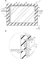
- FIG. 2A is a schematic cross-sectional view showing the same capacitor.
- FIG. 2B is an enlarged view of a portion surrounded by a broken line in FIG. 2A.
- 3A to 3D are schematic cross-sectional views showing the manufacturing process of the same capacitor.
- FIG. 4 is a perspective perspective view showing the capacitor according to the second embodiment.
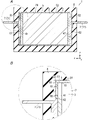
- FIG. 5A is a schematic cross-sectional view showing the same capacitor.
- FIG. 5B is an enlarged view of a portion surrounded by a broken line in FIG. 5A.
- 6A and 6B are schematic cross-sectional views showing the manufacturing process of the same capacitor.
- the capacitor 1 includes a capacitor element 2 and a protective film 5.
- the capacitor element 2 has a first end face electrode 41, a second end face electrode 42, and an outer peripheral surface 20.
- the second end face electrode 42 exists on the opposite side of the first end face electrode 41.
- the outer peripheral surface 20 exists between the first end surface electrode 41 and the second end surface electrode 42.
- the protective film 5 has a first protective unit 51, a second protective unit 52, and a third protective unit 53.
- the first protection portion 51 protects the peripheral edge portion of the first end face electrode 41.
- the second protective portion 52 protects the peripheral edge portion of the second end face electrode 42.
- the third protection unit 53 is connected to the first protection unit 51 and the second protection unit 52, and protects the outer peripheral surface 20.
- the boundary portion X1 between the main body 3 of the capacitor element 2 and the first end face electrode 41 is covered with a protective film 5 (particularly, a third protective portion 53). As a result, it is possible to prevent water from entering the inside of the main body 3 of the capacitor element 2 from the boundary portion X1.
- the boundary portion X2 exists between the first end face electrode 41 and the protective film 5 (particularly, the first protective portion 51), but the path from the boundary portion X2 to the boundary portion X1 is bent. .. Therefore, even if water infiltrates from the boundary portion X2, it is difficult to reach the boundary portion X1. The same applies to the second end face electrode 42 side. Moreover, the capacitor 1 does not require a case.
- FIGS. 1, 2A and 2B show the capacitor 1 according to this embodiment.
- the capacitor 1 is a so-called caseless capacitor. That is, unlike the case-molded capacitor of Patent Document 1, the capacitor 1 does not require a case. As a result, the weight of the capacitor 1 can be reduced.
- the capacitor 1 includes a capacitor element 2 and a protective film 5.
- the capacitor 1 may further include a bus bar 7 and a sealing portion 8.
- the capacitor element 2 of this embodiment is a so-called winding type capacitor element.
- the capacitor element 2 has a main body 3, a first end face electrode 41, and a second end face electrode 42 (see FIG. 2A).
- the main body 3 has two end faces (a surface facing a positive direction on the X-axis and a surface facing a negative direction on the X-axis) and an outer peripheral surface 20 existing between these two end faces.
- the main body 3 is formed by stacking two metallized films on which a metal such as aluminum is vapor-deposited on a dielectric film, winding the metallized film thus laminated, and pressing the film in a flat shape (Y-axis). It is formed by pressing in the direction).
- the cross-sectional shape of the main body 3 in the YZ plan view is a rounded rectangle that is longer in the Z-axis direction than in the Y-axis direction.
- the main body 3 has a pillar shape extending in the X-axis direction.
- the first end face electrode 41 and the second end face electrode 42 are provided in layers on the two end faces of the main body 3, respectively.
- the capacitor element 2 has a first end face electrode 41, a second end face electrode 42, and an outer peripheral surface 20. Similar to the main body 3, the cross-sectional shape of the capacitor element 2 in the YZ plan view is also a rounded rectangle longer in the Z-axis direction than in the Y-axis direction (see FIG. 1). Like the main body 3, the capacitor element 2 also has a columnar shape extending in the X-axis direction.
- the first end face electrode 41 exists on the surface of the capacitor element 2 facing the positive direction of the X axis.
- the first end face electrode 41 is made of a metal such as zinc by, for example, a metallikon (metal spraying method).
- the second end face electrode 42 exists on the opposite side of the first end face electrode 41. That is, the second end face electrode 42 exists on the surface of the capacitor element 2 facing the negative X-axis direction.
- the second end face electrode 42 is also formed in the same manner as the first end face electrode 41.
- the outer peripheral surface 20 of the capacitor element 2 is a surface constituting the outer peripheral surface of the capacitor element 2.
- the outer peripheral surface 20 includes the outer peripheral surface 20 of the main body 3 and exists between the first end surface electrode 41 and the second end surface electrode 42.
- the protective film 5 is a film having an electrical insulating property.
- the protective film 5 is preferably a film that does not easily allow moisture to permeate and can be fused.
- the material of the protective film 5 is not particularly limited, and examples thereof include polypropylene (PP), polyethylene (PE), polyvinyl chloride (PVC), and the like.
- the protective film 5 has a first protective unit 51, a second protective unit 52, and a third protective unit 53.
- the first protection unit 51 covers and protects a part of the first end face electrode 41.
- the first protective portion 51 includes a portion that protects the peripheral edge portion of the first end face electrode 41.
- the first protection unit 51 has an annular shape (see FIG. 1). Specifically, the outer peripheral edge of the first protection portion 51 forms a rounded rectangle that is longer in the Z-axis direction than in the Y-axis direction in the YZ plan view.
- the inner peripheral edge of the first protective portion 51 forms a rounded rectangle that is one size smaller than the rounded rectangle formed by the outer peripheral edge of the first protective portion 51.
- the portion between the outer peripheral edge and the inner peripheral edge of the first protective portion 51 corresponds to the peripheral edge portion of the first end face electrode 41.
- the second protection unit 52 covers and protects a part of the second end face electrode 42.
- the second protective portion 52 includes a portion that protects the peripheral edge portion of the second end face electrode 42.
- the second protection unit 52 is the same as the first protection unit 51. That is, the second protective portion 52 also forms an annular shape.
- the outer peripheral edge of the second protection portion 52 forms a rounded rectangle that is longer in the Z-axis direction than in the Y-axis direction in the YZ plan view.
- the inner peripheral edge of the second protective portion 52 forms a rounded rectangle that is one size smaller than the rounded rectangle formed by the outer peripheral edge of the second protective portion 52.
- the portion between the outer peripheral edge and the inner peripheral edge of the second protective portion 52 corresponds to the peripheral edge portion of the second end face electrode 42.
- the third protection unit 53 includes a portion that is connected to the first protection unit 51 and the second protection unit 52 and protects the outer peripheral surface 20.
- the third protection unit 53 has a tubular shape.
- the opening edge of one of the third protection portions 53 (on the positive side of the X-axis) is connected to the outer peripheral edge of the first protection portion 51.
- the other (X-axis negative side) opening edge of the third protection portion 53 is connected to the outer peripheral edge of the second protection portion 52.
- the third protection unit 53 covers and protects the outer peripheral surface 20 of the capacitor element 2.
- the protective film 5 includes a fused portion 50.
- the fused portion 50 is a portion bonded by applying pressure after heating. That is, welding is synonymous with welding.
- the fused portion 50 covers the entire inner surface of the first protective portion 51 (the surface facing the negative direction of the X-axis) and the entire inner surface of the second protective portion 52 (the surface facing the positive direction of the X-axis). Each exists.
- the fused portion 50 is adhered to the first end face electrode 41 and the second end face electrode 42. That is, the entire inner surface of the first protective portion 51 is adhered to the peripheral edge portion of the first end surface electrode 41, and the entire inner surface of the second protective portion 52 is adhered to the peripheral edge portion of the second end surface electrode 42.
- the bus bar 7 is a member (metal member) having conductivity.
- the bus bar 7 has an L shape in a ZX plan view.
- the bus bar 7 includes a first bus bar 71 and a second bus bar 72.
- the first bus bar 71 is electrically connected to the first end face electrode 41. Specifically, the first bus bar 71 is electrically connected to a surface of the first end surface electrode 41 that is not protected by the first protective portion 51 (a surface surrounded by the inner peripheral edge of the first protective portion 51). There is.
- the second bus bar 72 is electrically connected to the second end face electrode 42. Specifically, the second bus bar 72 is electrically connected to a surface of the second end surface electrode 42 that is not protected by the second protective portion 52 (a surface surrounded by the inner peripheral edge of the second protective portion 52). There is.
- the sealing portion 8 is a member having an electrical insulating property.
- the sealing portion 8 is preferably a member that does not easily allow moisture to permeate.
- the sealing material used to form the sealing portion 8 is not particularly limited, and examples thereof include an epoxy resin and the like.
- the sealing portion 8 seals the entire capacitor element 2.
- the sealing portion 8 forms a rectangular parallelepiped.
- the first bus bar 71 protrudes from one end surface (the surface facing the positive direction of the X-axis) of the sealing portion 8.
- the second bus bar 72 protrudes from the other end surface (the surface facing the negative direction of the X-axis) of the sealing portion 8.
- the method for manufacturing the capacitor 1 according to the present embodiment includes a preparation step, a winding step, and a fusion step.
- the method for manufacturing the capacitor 1 may further include a bus bar connecting step and a sealing step.
- the capacitor element 2 is prepared.
- the capacitor element 2 has a first end face electrode 41, a second end face electrode 42, and an outer peripheral surface 20.
- the length of the condenser element 2 in the X-axis direction that is, the distance between the first end face electrode 41 and the second end face electrode 42, more specifically, the surface of the first end face electrode 41 facing the X-axis positive direction).
- D be the distance in the X-axis direction between the second end surface electrode 42 and the surface facing the negative X-axis direction.
- the protective film 5 is wound around the outer peripheral surface 20 of the capacitor element 2 around the wire CL connecting the first end surface electrode 41 and the second end surface electrode 42.
- the line CL connecting the first end face electrode 41 and the second end face electrode 42 is a virtual straight line parallel to the X axis.
- the protective film 5 is as described above, but is a single film before being wound.
- the protective film 5 has a first protruding portion 510, a second protruding portion 520, and a third protective portion 53.
- the first protruding portion 510 is connected to the side edge of one of the third protective portions 53 (on the positive side of the X-axis).
- the first protruding portion 510 is a portion of the protective film 5 that protrudes from the first end surface electrode 41 side of the capacitor element 2.
- the first protruding portion 510 becomes the first protective portion 51.
- the second protruding portion 520 is connected to the other side edge (the negative side of the X-axis) of the third protective portion 53.
- the second protruding portion 520 becomes a portion of the protective film 5 that protrudes from the second end surface electrode 42 side of the capacitor element 2.
- the second protruding portion 520 becomes the second protective portion 52.
- the protective film 5 has a width W (see FIG. 3B).
- the width W is longer than the length D of the capacitor element 2 in the X-axis direction (distance D between the first end face electrode 41 and the second end face electrode 42).
- the difference between the width W and the distance D is equal to the sum of the lengths of the first protruding portion 510 and the second protruding portion 520 in the X-axis direction.
- the protective film 5 is projected from both ends of the capacitor element 2 (ends on the positive and negative sides of the X-axis), and the protective film 5 is formed on the outer peripheral surface of the capacitor element 2. Wind around 20.
- the first protruding portion 510 is made to protrude from the end on the positive side of the X-axis of the capacitor element 2.
- the second protruding portion 520 is projected from the end on the negative side of the X-axis of the capacitor element 2.
- the third protection unit 53 is arranged on the outer peripheral surface 20 of the capacitor element 2 and does not protrude from both ends of the capacitor element 2.
- the protective film 5 By winding the protective film 5 around the outer peripheral surface 20 of the capacitor element 2, the protective film 5 is laminated toward the radial outer side of the virtual circle in the YZ plane centered on the virtual straight line CL.
- the first protruding portion 510 projects in a cylindrical shape in the positive direction of the X-axis from one end of the capacitor element 2.
- the second protruding portion 520 projects in a cylindrical shape in the negative direction of the X-axis from the other end of the capacitor element 2.
- the number of turns of the protective film 5 is at least once, but is not particularly limited. The number of turns is appropriately determined in consideration of the thickness of the protective film 5 and the like.
- the first protrusion 510 is bent toward the first end face electrode 41 and fused to form the first protection portion 51.
- Welding includes heat welding, hot plate welding, ultrasonic welding, laser welding and the like.
- the second protective portion 52 is formed by bending and fusing the second protruding portion 520 toward the second end face electrode 42.
- the capacitor 1 according to the present embodiment is manufactured.
- the following steps are arbitrary steps.
- bus bar connection step As shown in FIG. 3D, the bus bar 7 is connected to the capacitor 1. Specifically, the first bus bar 71 is electrically connected to a surface not protected by the first protective portion 51 of the first end surface electrode 41. Further, the second bus bar 72 is electrically connected to the surface of the second end surface electrode 42 not protected by the second protective portion 52.
- the method of connecting the bus bar 7 to the capacitor 1 is not particularly limited, and examples thereof include welding and soldering.
- the sealing step the capacitor 1 to which the bus bar 7 is connected is sealed with resin. That is, the capacitor element 2 is installed in an appropriate mold, and a sealing material (for example, a thermosetting resin or the like) is injected into the entire periphery of the capacitor element 2 to form the sealing portion 8. As a result, the capacitor 1 shown in FIG. 1 is manufactured. In FIG. 1, the sealing portion 8 is illustrated by an imaginary line.
- a sealing material for example, a thermosetting resin or the like
- the boundary portion X1 between the main body 3 of the capacitor element 2 and the first end face electrode 41 is a protective film 5 (particularly, a third protective portion 53). ) Is covered. As a result, it is possible to prevent water from entering the inside of the main body 3 of the capacitor element 2 from the boundary portion X1.
- the boundary portion X2 exists between the first end face electrode 41 and the protective film 5 (particularly, the first protective portion 51), but the path from the boundary portion X2 to the boundary portion X1 is fused. Part 50 exists. Therefore, the fusional portion 50 tends to prevent the infiltration of water. Further, the path from the boundary portion X2 to the boundary portion X1 is bent. As a result, even if water infiltrates from the boundary portion X2, it is difficult to reach the boundary portion X1. The same applies to the second end face electrode 42 side. Moreover, the capacitor 1 does not require a case.
- the capacitor 1 according to the present embodiment it is possible to reduce moisture absorption while being lightweight. Further, according to the method for manufacturing a capacitor 1 according to the present embodiment, it is possible to manufacture a capacitor 1 that is lightweight and has excellent moisture resistance.
- the capacitor 1 according to the second embodiment will be described with reference to the drawings.
- the same components as those in the first embodiment may be designated by the same reference numerals as those in the first embodiment, and detailed description thereof may be omitted.
- FIGS. 4, 5A and 5B show the capacitor 1 according to this embodiment.
- the capacitor 1 according to the present embodiment is different from the capacitor 1 according to the first embodiment in that the capacitor element 2 further has a first additional electrode 61 and a second additional electrode 62.
- the first additional electrode 61 is an electrode additionally provided to the first end face electrode 41.
- the outer peripheral edge of the first additional electrode 61 is located outside the inner peripheral edge of the first protective portion 51 (broken line in FIG. 1). That is, the first additional electrode 61 covers the first protective portion 51 and the first end face electrode 41 not protected by the first protective portion 51.
- the outer peripheral edge of the first additional electrode 61 coincides with the outer peripheral edge of the first protection portion 51 in a YZ plan view.
- the first additional electrode 61 is electrically connected to the first end face electrode 41.
- the first additional electrode 61 is made of a metal such as zinc by, for example, a metallikon (metal spraying method).
- the second additional electrode 62 is the same as the first additional electrode 61. That is, the second additional electrode 62 is an electrode additionally provided to the second end face electrode 42. In a YZ plan view, the outer peripheral edge of the second additional electrode 62 is located outside the inner peripheral edge of the second protective portion 52. That is, the second additional electrode 62 covers the second protective portion 52 and the second end face electrode 42 that is not protected by the second protective portion 52. In particular, in the present embodiment, the outer peripheral edge of the second additional electrode 62 coincides with the outer peripheral edge of the second protective portion 52 in a YZ plan view.
- FIGS. 5A and 5B for convenience of explanation, a boundary line between the first additional electrode 61 and the first end face electrode 41 and a boundary line between the second additional electrode 62 and the second end face electrode 42. However, these boundaries may not be visible in practice.
- the method for manufacturing the capacitor 1 according to the present embodiment is different from the method for manufacturing the capacitor 1 according to the first embodiment in that it further includes an additional electrode forming step.
- the additional electrode forming step is a step after the fusion step shown in FIG. 3C.
- the additional electrode forming step as shown in FIG. 6A, the first additional electrode 61 and the second additional electrode 62 are formed by the metal spraying method.
- the first additional electrode 61 is formed by spraying a metal material onto the first protective portion 51 and the first end face electrode 41 not protected by the first protective portion 51.
- the metal material is not particularly limited, and examples thereof include zinc and the like.
- the second additional electrode 62 is formed by spraying a metal material onto the second protective portion 52 and the second end face electrode 42 not protected by the second protective portion 52.
- the metal material used to form the second additional electrode 62 may be the same as or different from the metal material used to form the first additional electrode 61.
- the capacitor 1 according to the present embodiment is manufactured.
- the following steps are arbitrary steps.
- bus bar connection step As shown in FIG. 6B, the bus bar 7 is connected to the capacitor 1. Specifically, the first bus bar 71 is electrically connected to the first additional electrode 61. Further, the second bus bar 72 is electrically connected to the second additional electrode 62.
- the method of connecting the bus bar 7 to the capacitor 1 is not particularly limited, and examples thereof include welding and soldering.
- the sealing step the capacitor 1 to which the bus bar 7 is connected is sealed with resin. That is, the capacitor element 2 is installed in an appropriate mold, and a sealing material (for example, a thermosetting resin or the like) is injected into the entire periphery of the capacitor element 2 to form the sealing portion 8. As a result, the capacitor 1 shown in FIG. 4 is manufactured. In FIG. 4, the sealing portion 8 is illustrated by an imaginary line.
- a sealing material for example, a thermosetting resin or the like
- This embodiment also has basically the same action and effect as the first embodiment. That is, in the present embodiment, as shown in FIG. 5B, the boundary portion X1 between the main body 3 of the capacitor element 2 and the first end face electrode 41 is covered with the protective film 5 (particularly, the third protective portion 53). There is. As a result, it is possible to prevent water from entering the inside of the main body 3 of the capacitor element 2 from the boundary portion X1.
- the boundary portion X2 exists between the first end face electrode 41 and the protective film 5 (particularly, the first protective portion 51), but the path from the boundary portion X2 to the boundary portion X1 is fused. Part 50 exists. Therefore, the fusional portion 50 tends to prevent the infiltration of water.
- the boundary portion X3 exists between the first additional electrode 61 and the protective film 5 (particularly, the first protective portion 51), but the boundary portion X3 passes through the boundary portion X2.
- the path leading to the boundary portion X1 is bent more than in the case of the first embodiment.
- the capacitor 1 does not require a case.
- the capacitor 1 according to the present embodiment it is possible to reduce moisture absorption while being lightweight. Further, according to the method for manufacturing a capacitor 1 according to the present embodiment, it is possible to manufacture a capacitor 1 that is lightweight and has excellent moisture resistance.
- the capacitor element 2 is a winding type capacitor element, but may be a laminated type capacitor element.
- the inner surface of the first protective portion 51 is adhered to the first end face electrode 41, and the inner surface of the second protective portion 52 is adhered to the second end face electrode 42, but the third protective portion 53 is further adhered to.
- the inner peripheral surface of the capacitor element 2 may be adhered to the outer peripheral surface 20 of the capacitor element 2. That is, the fused portion 50 may be present on at least a part of the inner peripheral surface of the third protective portion 53.
- the fused portion 50 exists on the entire inner surface of the first protective portion 51 and the entire inner surface of the second protected portion 52, respectively, but the fused portion 50 may exist so as to form a closed curve. good. That is, the fused portion 50 of the first protected portion 51 surrounds the inner peripheral edge of the first protected portion 51 and forms a closed curve surrounded by the outer peripheral edge of the first protected portion 51. It may exist on the inner surface of.
- the fused portion 50 of the second protective portion 52 also has a second protective portion so as to form a closed curve surrounding the inner peripheral edge of the second protective portion 52 and surrounded by the outer peripheral edge of the second protective portion 52. It may be present on the inner surface of 52.
- the shape and size of the first bus bar 71 and the second bus bar 72 are the same, but may be different.
- the protruding directions of the first bus bar 71 and the second bus bar 72 are opposite to each other, but the protruding directions of the first bus bar 71 and the second bus bar 72 may be the same direction, and are not particularly limited.
- the sealing portion 8 has a rectangular parallelepiped shape, but the sealing portion 8 may have a three-dimensional shape other than the rectangular parallelepiped shape.
- the outer peripheral edge of the first additional electrode 61 coincides with the outer peripheral edge of the first protective portion 51, but is not particularly limited as long as it is outside the inner peripheral edge of the first protective portion 51. That is, the boundary portion X3 exists on the outer peripheral edge of the first protection portion 51, but the boundary portion X3 is outside the first protection portion 51 on the surface of the first protection portion 51 facing in the positive direction of the X axis. It may exist between the peripheral edge and the inner peripheral edge. The same applies to the case of the second additional electrode 62.
- the first aspect is a capacitor (1), which includes a capacitor element (2) and a protective film (5).
- the capacitor element (2) has a first end face electrode (41), a second end face electrode (42), and an outer peripheral surface (20).
- the second end face electrode (42) exists on the opposite side of the first end face electrode (41).
- the outer peripheral surface (20) exists between the first end face electrode (41) and the second end face electrode (42).
- the protective film (5) has a first protective portion (51), a second protective portion (52), and a third protective portion (53).
- the first protective portion (51) protects the peripheral edge portion of the first end face electrode (41).
- the second protective portion (52) protects the peripheral edge portion of the second end face electrode (42).
- the third protective portion (53) is connected to the first protective portion (51) and the second protective portion (52), and protects the outer peripheral surface (20).
- the second aspect is the capacitor (1) based on the first aspect.
- the protective film (5) includes a fused portion (50). The fused portion (50) is adhered to the first end face electrode (41) and the second end face electrode (42).
- moisture absorption can be further reduced.
- the third aspect is the capacitor (1) based on the first or second aspect.
- the capacitor element (2) further has a first additional electrode (61) and a second additional electrode (62).
- the first additional electrode (61) covers the first protective portion (51) and the first end face electrode (41) not protected by the first protective portion (51).
- the second additional electrode (62) covers the second protective portion (52) and the second end face electrode (42) that is not protected by the second protective portion (52).
- moisture absorption can be further reduced.
- the fourth aspect is a method for manufacturing a capacitor (1), which includes a preparation step, a winding step, and a fusion step.
- the first end face electrode (41), the second end face electrode (42) existing on the opposite side of the first end face electrode (41), the first end face electrode (41), and the second end face A capacitor element (2) having an outer peripheral surface (20) existing between the electrodes (42) is prepared.
- the capacitor element is provided with a protective film (5) having a width (W) longer than the distance (D) between the first end face electrode (41) and the second end face electrode (42). It is wound around the outer peripheral surface (20) while protruding from both ends of (2).
- the first protruding portion (510) protruding from the first end surface electrode (41) side of the protective film (5) is bent toward the first end surface electrode (41) and fused.
- the first protective portion (51) that protects the peripheral edge portion of the first end surface electrode (41) is formed, and the protective film (5) protrudes from the second end surface electrode (42) side.
- the protruding portion (520) is bent toward the second end face electrode (42) and fused to form a second protective portion (52) that protects the peripheral edge portion of the second end face electrode (42). do.
- the fifth aspect is the method for manufacturing the capacitor (1) based on the fourth aspect.
- a fifth aspect further comprises an additional electrode forming step.
- the first addition is performed by spraying a metal material onto the first protective portion (51) and the first end face electrode (41) not protected by the first protective portion (51).
- the second additional electrode (62) is formed.
- Capacitor 2 Capacitor element 20 Outer peripheral surface 41 First end face electrode 42 Second end face electrode 5 Protective film 51 First protection part 52 Second protection part 53 Third protection part 61 First additional electrode 62 Second additional electrode D Distance W width
Landscapes
- Engineering & Computer Science (AREA)
- Power Engineering (AREA)
- Manufacturing & Machinery (AREA)
- Microelectronics & Electronic Packaging (AREA)
- Fixed Capacitors And Capacitor Manufacturing Machines (AREA)
Priority Applications (2)
| Application Number | Priority Date | Filing Date | Title |
|---|---|---|---|
| JP2022566804A JP7836998B2 (ja) | 2020-12-02 | 2021-11-09 | コンデンサ及びその製造方法 |
| US18/314,172 US12542241B2 (en) | 2020-12-02 | 2023-05-09 | Capacitor and manufacturing method thereof |
Applications Claiming Priority (2)
| Application Number | Priority Date | Filing Date | Title |
|---|---|---|---|
| JP2020200497 | 2020-12-02 | ||
| JP2020-200497 | 2020-12-02 |
Related Child Applications (1)
| Application Number | Title | Priority Date | Filing Date |
|---|---|---|---|
| US18/314,172 Continuation US12542241B2 (en) | 2020-12-02 | 2023-05-09 | Capacitor and manufacturing method thereof |
Publications (1)
| Publication Number | Publication Date |
|---|---|
| WO2022118616A1 true WO2022118616A1 (ja) | 2022-06-09 |
Family
ID=81853688
Family Applications (1)
| Application Number | Title | Priority Date | Filing Date |
|---|---|---|---|
| PCT/JP2021/041252 Ceased WO2022118616A1 (ja) | 2020-12-02 | 2021-11-09 | コンデンサ及びその製造方法 |
Country Status (3)
| Country | Link |
|---|---|
| US (1) | US12542241B2 (https=) |
| JP (1) | JP7836998B2 (https=) |
| WO (1) | WO2022118616A1 (https=) |
Cited By (1)
| Publication number | Priority date | Publication date | Assignee | Title |
|---|---|---|---|---|
| WO2024070067A1 (ja) * | 2022-09-30 | 2024-04-04 | 株式会社村田製作所 | フィルムコンデンサ及びモジュール |
Citations (4)
| Publication number | Priority date | Publication date | Assignee | Title |
|---|---|---|---|---|
| JP2008098675A (ja) * | 2007-12-27 | 2008-04-24 | Matsushita Electric Ind Co Ltd | 偏平形金属化フィルムコンデンサ |
| JP2016207828A (ja) * | 2015-04-22 | 2016-12-08 | ニチコン株式会社 | コンデンサ素子およびその製造方法 |
| WO2020044778A1 (ja) * | 2018-08-28 | 2020-03-05 | パナソニックIpマネジメント株式会社 | コンデンサ及びその製造方法 |
| JP2020136518A (ja) * | 2019-02-20 | 2020-08-31 | パナソニックIpマネジメント株式会社 | コンデンサ及びコンデンサの製造方法 |
Family Cites Families (8)
| Publication number | Priority date | Publication date | Assignee | Title |
|---|---|---|---|---|
| US3452257A (en) * | 1968-03-28 | 1969-06-24 | Vitramon Inc | Electrical capacitor |
| CA1112729A (en) * | 1977-11-19 | 1981-11-17 | Tomiji Kobayashi | Tubular capacitor and method of making the same |
| JPH0442905Y2 (https=) * | 1986-06-09 | 1992-10-12 | ||
| JPH0236024U (https=) * | 1988-09-02 | 1990-03-08 | ||
| US5912796A (en) * | 1996-11-15 | 1999-06-15 | Illinois Tool Works, Inc. | Metallized film capacitor and manufacturing process |
| JP2006294788A (ja) | 2005-04-08 | 2006-10-26 | Matsushita Electric Ind Co Ltd | ケースモールド型コンデンサ及びこれを用いたインバータ回路、車両駆動用モータの駆動回路 |
| JP6439141B2 (ja) | 2015-02-24 | 2018-12-19 | パナソニックIpマネジメント株式会社 | 金属化フィルムコンデンサ |
| CN113228210B (zh) * | 2018-12-26 | 2023-04-28 | 松下知识产权经营株式会社 | 电容器 |
-
2021
- 2021-11-09 JP JP2022566804A patent/JP7836998B2/ja active Active
- 2021-11-09 WO PCT/JP2021/041252 patent/WO2022118616A1/ja not_active Ceased
-
2023
- 2023-05-09 US US18/314,172 patent/US12542241B2/en active Active
Patent Citations (4)
| Publication number | Priority date | Publication date | Assignee | Title |
|---|---|---|---|---|
| JP2008098675A (ja) * | 2007-12-27 | 2008-04-24 | Matsushita Electric Ind Co Ltd | 偏平形金属化フィルムコンデンサ |
| JP2016207828A (ja) * | 2015-04-22 | 2016-12-08 | ニチコン株式会社 | コンデンサ素子およびその製造方法 |
| WO2020044778A1 (ja) * | 2018-08-28 | 2020-03-05 | パナソニックIpマネジメント株式会社 | コンデンサ及びその製造方法 |
| JP2020136518A (ja) * | 2019-02-20 | 2020-08-31 | パナソニックIpマネジメント株式会社 | コンデンサ及びコンデンサの製造方法 |
Cited By (2)
| Publication number | Priority date | Publication date | Assignee | Title |
|---|---|---|---|---|
| WO2024070067A1 (ja) * | 2022-09-30 | 2024-04-04 | 株式会社村田製作所 | フィルムコンデンサ及びモジュール |
| JPWO2024070067A1 (https=) * | 2022-09-30 | 2024-04-04 |
Also Published As
| Publication number | Publication date |
|---|---|
| US20230326675A1 (en) | 2023-10-12 |
| JP7836998B2 (ja) | 2026-03-30 |
| JPWO2022118616A1 (https=) | 2022-06-09 |
| US12542241B2 (en) | 2026-02-03 |
Similar Documents
| Publication | Publication Date | Title |
|---|---|---|
| JP7217404B2 (ja) | コンデンサ | |
| US9190633B2 (en) | Pouch type lithium secondary battery | |
| JP6439141B2 (ja) | 金属化フィルムコンデンサ | |
| JP7083419B2 (ja) | ケースレスフィルムコンデンサ | |
| JP2011135753A (ja) | モータ | |
| US11935697B2 (en) | Capacitor | |
| WO2022118616A1 (ja) | コンデンサ及びその製造方法 | |
| JP2020136518A (ja) | コンデンサ及びコンデンサの製造方法 | |
| JP7390559B2 (ja) | コンデンサ | |
| JP2005019213A (ja) | 電気リード部の構造、該リード部構造を有する電気デバイス、電池および組電池 | |
| US11038228B2 (en) | Electrochemical device having a thermally fusible resin layer | |
| JP7357223B2 (ja) | コンデンサ | |
| KR20160058707A (ko) | 리드 부재 및 전지 | |
| JP2020017401A (ja) | 蓄電装置及び蓄電装置の製造方法 | |
| JP2024012698A (ja) | コンデンサ | |
| CN207398188U (zh) | 壳体及电池 | |
| JP5653242B2 (ja) | フィルムコンデンサ | |
| JP3058090B2 (ja) | 固体電解コンデンサ | |
| JP3880804B2 (ja) | 電気二重層キャパシタ及びその製造方法 | |
| CN215869705U (zh) | 极耳结构及扣式电池 | |
| JP2021132166A (ja) | コンデンサ | |
| JP6473989B2 (ja) | コンデンサ | |
| JP2021132165A (ja) | コンデンサ | |
| JP2536242Y2 (ja) | 複合コンデンサ | |
| JP2021150399A (ja) | コンデンサ及びコンデンサの製造方法 |
Legal Events
| Date | Code | Title | Description |
|---|---|---|---|
| 121 | Ep: the epo has been informed by wipo that ep was designated in this application |
Ref document number: 21900371 Country of ref document: EP Kind code of ref document: A1 |
|
| ENP | Entry into the national phase |
Ref document number: 2022566804 Country of ref document: JP Kind code of ref document: A |
|
| NENP | Non-entry into the national phase |
Ref country code: DE |
|
| 122 | Ep: pct application non-entry in european phase |
Ref document number: 21900371 Country of ref document: EP Kind code of ref document: A1 |