WO2022113779A1 - 積層基板および積層基板の製造方法 - Google Patents
積層基板および積層基板の製造方法 Download PDFInfo
- Publication number
- WO2022113779A1 WO2022113779A1 PCT/JP2021/041721 JP2021041721W WO2022113779A1 WO 2022113779 A1 WO2022113779 A1 WO 2022113779A1 JP 2021041721 W JP2021041721 W JP 2021041721W WO 2022113779 A1 WO2022113779 A1 WO 2022113779A1
- Authority
- WO
- WIPO (PCT)
- Prior art keywords
- laminated substrate
- opening
- conductor
- view
- conductor pattern
- Prior art date
- Legal status (The legal status is an assumption and is not a legal conclusion. Google has not performed a legal analysis and makes no representation as to the accuracy of the status listed.)
- Ceased
Links
Images


Classifications
-
- H—ELECTRICITY
- H05—ELECTRIC TECHNIQUES NOT OTHERWISE PROVIDED FOR
- H05K—PRINTED CIRCUITS; CASINGS OR CONSTRUCTIONAL DETAILS OF ELECTRIC APPARATUS; MANUFACTURE OF ASSEMBLAGES OF ELECTRICAL COMPONENTS
- H05K1/00—Printed circuits
- H05K1/02—Details
- H05K1/0213—Electrical arrangements not otherwise provided for
- H05K1/0216—Reduction of cross-talk, noise or electromagnetic interference
- H05K1/0218—Reduction of cross-talk, noise or electromagnetic interference by printed shielding conductors, ground planes or power plane
- H05K1/0224—Patterned shielding planes, ground planes or power planes
- H05K1/0225—Single or multiple openings in a shielding, ground or power plane
-
- H—ELECTRICITY
- H05—ELECTRIC TECHNIQUES NOT OTHERWISE PROVIDED FOR
- H05K—PRINTED CIRCUITS; CASINGS OR CONSTRUCTIONAL DETAILS OF ELECTRIC APPARATUS; MANUFACTURE OF ASSEMBLAGES OF ELECTRICAL COMPONENTS
- H05K1/00—Printed circuits
- H05K1/02—Details
- H05K1/0213—Electrical arrangements not otherwise provided for
- H05K1/0216—Reduction of cross-talk, noise or electromagnetic interference
- H05K1/0218—Reduction of cross-talk, noise or electromagnetic interference by printed shielding conductors, ground planes or power plane
- H05K1/0219—Printed shielding conductors for shielding around or between signal conductors, e.g. coplanar or coaxial printed shielding conductors
-
- H—ELECTRICITY
- H05—ELECTRIC TECHNIQUES NOT OTHERWISE PROVIDED FOR
- H05K—PRINTED CIRCUITS; CASINGS OR CONSTRUCTIONAL DETAILS OF ELECTRIC APPARATUS; MANUFACTURE OF ASSEMBLAGES OF ELECTRICAL COMPONENTS
- H05K1/00—Printed circuits
- H05K1/02—Details
- H05K1/0213—Electrical arrangements not otherwise provided for
- H05K1/0216—Reduction of cross-talk, noise or electromagnetic interference
- H05K1/0218—Reduction of cross-talk, noise or electromagnetic interference by printed shielding conductors, ground planes or power plane
- H05K1/0224—Patterned shielding planes, ground planes or power planes
-
- H—ELECTRICITY
- H05—ELECTRIC TECHNIQUES NOT OTHERWISE PROVIDED FOR
- H05K—PRINTED CIRCUITS; CASINGS OR CONSTRUCTIONAL DETAILS OF ELECTRIC APPARATUS; MANUFACTURE OF ASSEMBLAGES OF ELECTRICAL COMPONENTS
- H05K1/00—Printed circuits
- H05K1/02—Details
- H05K1/0277—Bendability or stretchability details
- H05K1/028—Bending or folding regions of flexible printed circuits
-
- H—ELECTRICITY
- H05—ELECTRIC TECHNIQUES NOT OTHERWISE PROVIDED FOR
- H05K—PRINTED CIRCUITS; CASINGS OR CONSTRUCTIONAL DETAILS OF ELECTRIC APPARATUS; MANUFACTURE OF ASSEMBLAGES OF ELECTRICAL COMPONENTS
- H05K1/00—Printed circuits
- H05K1/02—Details
- H05K1/0296—Conductive pattern lay-out details not covered by sub groups H05K1/02 - H05K1/0295
- H05K1/0298—Multilayer circuits
-
- H—ELECTRICITY
- H05—ELECTRIC TECHNIQUES NOT OTHERWISE PROVIDED FOR
- H05K—PRINTED CIRCUITS; CASINGS OR CONSTRUCTIONAL DETAILS OF ELECTRIC APPARATUS; MANUFACTURE OF ASSEMBLAGES OF ELECTRICAL COMPONENTS
- H05K1/00—Printed circuits
- H05K1/02—Details
- H05K1/0213—Electrical arrangements not otherwise provided for
- H05K1/0237—High frequency adaptations
- H05K1/024—Dielectric details, e.g. changing the dielectric material around a transmission line
-
- H—ELECTRICITY
- H05—ELECTRIC TECHNIQUES NOT OTHERWISE PROVIDED FOR
- H05K—PRINTED CIRCUITS; CASINGS OR CONSTRUCTIONAL DETAILS OF ELECTRIC APPARATUS; MANUFACTURE OF ASSEMBLAGES OF ELECTRICAL COMPONENTS
- H05K2201/00—Indexing scheme relating to printed circuits covered by H05K1/00
- H05K2201/01—Dielectrics
- H05K2201/0104—Properties and characteristics in general
- H05K2201/0129—Thermoplastic polymer, e.g. auto-adhesive layer; Shaping of thermoplastic polymer
-
- H—ELECTRICITY
- H05—ELECTRIC TECHNIQUES NOT OTHERWISE PROVIDED FOR
- H05K—PRINTED CIRCUITS; CASINGS OR CONSTRUCTIONAL DETAILS OF ELECTRIC APPARATUS; MANUFACTURE OF ASSEMBLAGES OF ELECTRICAL COMPONENTS
- H05K2201/00—Indexing scheme relating to printed circuits covered by H05K1/00
- H05K2201/01—Dielectrics
- H05K2201/0137—Materials
- H05K2201/0141—Liquid crystal polymer [LCP]
-
- H—ELECTRICITY
- H05—ELECTRIC TECHNIQUES NOT OTHERWISE PROVIDED FOR
- H05K—PRINTED CIRCUITS; CASINGS OR CONSTRUCTIONAL DETAILS OF ELECTRIC APPARATUS; MANUFACTURE OF ASSEMBLAGES OF ELECTRICAL COMPONENTS
- H05K2201/00—Indexing scheme relating to printed circuits covered by H05K1/00
- H05K2201/07—Electric details
- H05K2201/0707—Shielding
- H05K2201/0715—Shielding provided by an outer layer of PCB
-
- H—ELECTRICITY
- H05—ELECTRIC TECHNIQUES NOT OTHERWISE PROVIDED FOR
- H05K—PRINTED CIRCUITS; CASINGS OR CONSTRUCTIONAL DETAILS OF ELECTRIC APPARATUS; MANUFACTURE OF ASSEMBLAGES OF ELECTRICAL COMPONENTS
- H05K3/00—Apparatus or processes for manufacturing printed circuits
- H05K3/0011—Working of insulating substrates or insulating layers
- H05K3/0017—Etching of the substrate by chemical or physical means
- H05K3/002—Etching of the substrate by chemical or physical means by liquid chemical etching
Definitions
- the present invention relates to a laminated substrate in which a plurality of insulating layers are laminated, and a method for manufacturing the laminated substrate.
- Patent Document 1 a laminated substrate in which a plurality of insulating layers in which conductors are patterned are laminated (see, for example, Patent Document 1).
- a portion of the ground conductor on the surface that does not overlap with the signal line in a plan view is removed, and a recess or a hole is provided in the insulating layer.
- the laminated substrate of Patent Document 1 is a resin laminated substrate capable of increasing flexibility without deteriorating the electrical characteristics of the transmission line.
- an object of the present invention is to provide a laminated substrate and a method for manufacturing a laminated substrate that can improve the electrical characteristics of a transmission line.
- the laminated substrate of the present invention is a laminated substrate formed by laminating a plurality of insulating layers having conductors formed on its main surface, and is composed of a signal line composed of the conductors and a plane formed on the signal lines.
- a shield conductor having an overlapping portion when viewed is provided, the shield conductor is provided with an opening, the insulating layer communicates with the opening, and a hole larger than the opening is formed in a plan view. There is.
- the dielectric constant and the dielectric loss can be reduced while preventing the deterioration of the shielding property.
- the electrical characteristics of the transmission line can be improved.
- the electrical characteristics of the transmission line can be improved.
- FIG. 5 (A) is a cross-sectional view of the laminated substrate 1A according to the modified example 1
- FIG. 5 (B) is a cross-sectional view of the laminated substrate 1B according to the modified example 2.
- FIG. 7A is a cross-sectional view of the laminated substrate 1D according to the modified example 4
- FIG. 7B is a cross-sectional view of the laminated substrate 1E according to the modified example 5.
- FIG. 8 (A) to 8 (C) are plan views showing a modified example of the shape of the opening. It is a side sectional view of the laminated substrate 1F at the position shown by AA in FIG. 8A. It is a top view of the laminated substrate 1G in which the conductor pattern 50A and the conductor pattern 50B are formed.
- 11 (A) is a plan view of the laminated substrate 1H having a bending region 90
- FIG. 11 (B) is a plan view of the laminated substrate 1I having a bending region 90
- FIG. 11 (C) is a bending view.
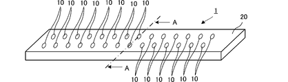
- FIG. 1 is a perspective view of the laminated substrate 1.
- FIG. 2 is a plan view of the laminated substrate 1.
- FIG. 3 is a side sectional view of the laminated substrate 1 at the position indicated by AA in FIG. 2.
- the laminated substrate 1 has a rectangular parallelepiped shape that is long in one direction.
- the laminated board 1 includes terminals and the like for mounting (not shown).
- the laminated substrate 1 is formed by laminating the resin base material 11A, the resin base material 11B, the resin base material 11C, and the resin base material 11D in order from the upper surface side.
- the resin base material 11A, the resin base material 11B, the resin base material 11C, and the resin base material 11D are examples of the insulating layer of the present invention, respectively.
- the number of layers of the insulating layer is not limited to the number of layers shown in the present embodiment.
- the resin base material 11A, the resin base material 11B, the resin base material 11C, and the resin base material 11D are made of the same type of thermoplastic resin.
- the thermoplastic resin is, for example, a liquid crystal polymer resin.
- Thermoplastic resins other than the liquid crystal polymer resin include, for example, PEEK (polyetheretherketone), PEI (polyetherimide), PPS (ponylenesulfide), PI (polyimide), etc., and these are used instead of the liquid crystal polymer resin. You may use it.
- the insulating layer of the present invention is not limited to the thermoplastic resin, and for example, ceramic or the like can be used.
- Each resin base material has a conductor (for example, copper) formed on the upper surface or the lower surface.
- the resin base material 11A has a conductor pattern 20 formed on the upper surface thereof.
- a conductor pattern 131A is formed on the upper surface of the resin base material 11B.
- the conductor pattern 50 and the conductor pattern 131B are formed on the upper surface of the resin base material 11C.
- the resin base material 11D has a conductor pattern 30 formed on the lower surface thereof. Each conductor pattern is formed before laminating.
- the conductor pattern 20 and the conductor pattern 30 have a reference potential (ground potential) and function as a shield conductor.
- the conductor pattern 50 functions as a signal line.
- the conductor pattern 20 covers the upper surface of the laminated substrate 1, and the conductor pattern 30 covers the lower surface of the laminated substrate 1.
- the conductor pattern 50 is formed in a long rectangular shape along the long axis direction of the laminated substrate 1 in a plan view.
- the arrangement mode of the signal line and the shield conductor is not limited to the structure shown in this embodiment.
- the present invention may include at least a signal line and a shield conductor having a portion that overlaps the signal line in a plan view.
- the resin base material 11A is provided with an interlayer connecting conductor 13A.
- the conductor pattern 20 and the conductor pattern 131A are electrically connected by the interlayer connecting conductor 13A.
- the resin base material 11B is provided with an interlayer connecting conductor 13B.
- the conductor pattern 131A and the conductor pattern 131B are electrically connected by the interlayer connecting conductor 13B.
- the resin base material 11C is provided with an interlayer connecting conductor 13C
- the resin base material 11D is provided with an interlayer connecting conductor 13D.
- the interlayer connecting conductor 13C and the interlayer connecting conductor 13D overlap each other in a plan view (viewed from the stacking direction), and are in direct contact with each other without a conductor pattern.
- the conductor pattern 131B and the conductor pattern 30 are electrically connected by the interlayer connecting conductor 13C and the interlayer connecting conductor 13D.
- the conductor pattern 20 and the conductor pattern 30 are provided with an opening 10.
- the opening 10 has a circular shape in a plan view.
- the diameter of the opening 10 is smaller than the width of the conductor pattern 30. Since the diameter of the opening 10 is smaller than the width of the conductor pattern 30, noise radiation can be suppressed.
- a plurality of openings 10 are provided at equal pitches so as to sandwich the conductor pattern 30 in the width direction in a plan view. In the example of FIG. 2, the pitch in which the opening 10 is formed is twice the diameter of the opening 10.
- the number, shape, size, pitch, and the like of the openings 10 are not limited to the examples of the present embodiment. Also, the shapes and sizes of all openings 10 do not have to be the same.
- a hole 15 is provided in the resin base material 11A at a position overlapping the opening 10 in a plan view.
- the resin base material 11D is also provided with a hole 15 at a position overlapping the opening 10 in a plan view.
- the holes 15 are formed by etching the resin base material 11A and the resin base material 11D from the openings 10.
- the resin base material 11A and the resin base material 11D are removed not only directly under the opening 10 but also directly under the conductor pattern 20 and the conductor pattern 30 by isotropic etching.
- the hole 15 communicates with the opening 10.
- the diameter of the hole 15 is larger than the diameter of the opening 10 in a plan view. It is preferable that the distance between the interlayer connecting conductor 13A (interlayer connecting conductor 13D) and the opening 10 is, for example, greater than or equal to the diameter of the opening 10.
- the insulating layer is removed directly under the conductor pattern 20 and the conductor pattern 30, which are shield conductors. In the place where the insulating layer is removed, the dielectric constant and the dielectric loss are lower than in the part where the insulating layer is present. On the other hand, since the place where the insulating layer is removed is directly under the conductor pattern 20 and the conductor pattern 30, the shielding property does not deteriorate. As a result, the laminated substrate 1 of the present embodiment can reduce the dielectric constant and the dielectric loss while preventing the deterioration of the shielding property, and can improve the electrical characteristics as a transmission line.
- FIG. 4 is a diagram showing a method of manufacturing a laminated substrate.
- a resin base material as an insulating layer is prepared, a conductor pattern is formed, and a circuit forming step (S11) for forming a circuit is performed.
- the resin base material is prepared by cutting out a required area from a resin sheet in which a metal (for example, copper foil) is previously attached to the entire main surface of one side.
- the resin base material 11 forms a conductor pattern by patterning a copper foil.
- the patterning method for example, photolithography or screen printing is used.
- the opening 10 is formed when the conductor pattern 20 and the conductor pattern 30 are formed. However, it may be formed after laminating the resin base material or after hot pressing.
- a through hole penetrating the resin base material is formed in the laminating direction by laser processing or the like, and an interlayer connection conductor is formed by filling with a conductive paste (S12).
- the conductive paste is made of a conductive material containing tin or copper as a main component.
- each insulating layer (resin base material 11A, resin base material 11B, resin base material 11C, and resin base material 11D) is laminated (S13). After that, the laminated substrate 1 is formed by performing a hot press (S14) with a hot press machine.
- a portion where the insulating layer is exposed other than the opening 10 such as a terminal (not shown) is masked (S15), and etching is performed to form a hole 15 (S16).
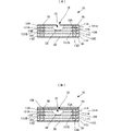
- FIG. 5A is a cross-sectional view of the laminated substrate 1A according to the modified example 1.
- the configurations common to those in FIG. 3 are designated by the same reference numerals, and the description thereof will be omitted.
- the opening 10 and the hole 15 are formed only on the main surface on the conductor pattern 20 side.
- the openings 10 and the holes 15 may be formed only on the main surface on the conductor pattern 30 side.
- FIG. 5B is a cross-sectional view of the laminated substrate 1B according to the modified example 2.
- the configurations common to those in FIG. 3 are designated by the same reference numerals, and the description thereof will be omitted.
- the pores 15 of the laminated substrate 1B according to the second modification are formed so as to straddle a plurality of insulating layers.
- the pores 15 are formed so as to straddle the resin base material 11A and the resin base material 11B. In this way, the pores 15 may be formed across a plurality of insulating layers.
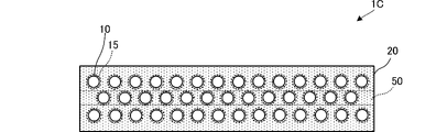
- FIG. 6 is a plan view of the laminated substrate 1C according to the modified example 3.
- the opening 10 may overlap the conductor pattern 50, which is a signal line in a plan view.
- the conductor pattern 50 which is a signal line in a plan view.
- the holes 15 do not necessarily have to overlap the conductor pattern 50 in a plan view.
- the electric field formed on the conductor pattern 50 and the shield conductor is not limited to the overlapping position of the conductor pattern 50 and the shield conductor.
- the dielectric constant and the dielectric loss can be reduced if they are formed in the vicinity of the conductor pattern 50, and the electrical characteristics of the transmission line are improved. Can be made to.
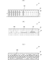
- FIG. 7A is a cross-sectional view of the laminated substrate 1D according to the modified example 4.
- the configurations common to those in FIG. 3 are designated by the same reference numerals, and the description thereof will be omitted.
- the opening 10 of the laminated substrate 1D according to the modified example 4 overlaps with the conductor pattern 50 in a plan view. Further, the pores 15 reach the conductor pattern 50. That is, the opening 10 and the conductor pattern 50 communicate with each other through the holes 15. In this case, the dielectric constant and the dielectric loss can be further reduced.
- FIG. 7B is a cross-sectional view of the laminated substrate 1E according to the modified example 5.
- the cover layer 100 is made of, for example, PET (polyethylene terephthalate). Due to the cover layer 100, the conductor pattern 50 is not exposed to the outside. Since the pores 15 are maintained even if the cover layer 100 is covered, the dielectric constant and the dielectric loss can be further reduced as in the laminated substrate 1D.
- FIGS. 8 (A) to 8 (C) are plan views showing a modified example of the shape of the opening.
- the number, shape, size, pitch, and the like of the openings are not limited to the examples shown in the plan view of FIG.
- the opening 10A may be long along the width direction of the laminated substrate 1F, or as shown in FIG. 8B, the opening 10B long along the long side direction of the laminated substrate 1G. May be.
- the opening 10C may have the conductor pattern 20 removed in a mesh shape.
- FIG. 9 is a side sectional view of the laminated substrate 1F at the position indicated by AA in FIG. 8A.
- the holes communicating with each opening may be connected to each other.
- the example of FIG. 9 shows a hole 15A formed by connecting a plurality of holes communicating with each other to the plurality of openings 10A.
- the shield conductor may be floating from the insulating layer when viewed in a certain cross section.
- the pitch of the opening 10A is smaller than the depth of the hole 15A.
- FIG. 10 is a plan view of the laminated substrate 1G on which the conductor pattern 50A and the conductor pattern 50B are formed.
- the conductor pattern 50A and the conductor pattern 50B form a differential transmission line.
- the openings 10 and the holes 15 are arranged symmetrically side by side in the width direction of the laminated substrate 1G with the axis of symmetry of the differential transmission line interposed therebetween. Therefore, the laminated substrate 1G can maintain the symmetry of the electrical characteristics of the conductor pattern 50A and the conductor pattern 50B, and can improve the characteristics of the transmission line.
- FIG. 11 (A) is a plan view of the laminated substrate 1H having a bending region 90
- FIG. 11 (B) is a plan view of the laminated substrate 1I having a bending region 90
- FIG. 11 (C) is a bending view. It is a top view of the laminated substrate 1J which has a region 90.
- the laminated substrate 1H of FIG. 11A has a bending region 90 at the center in the long axis direction.
- the bent region 90 is not provided with an opening 10 and a hole 15. Therefore, in the laminated substrate 1H, when the bending region 90 is bent along the laminating direction, the shield conductor is not destroyed from the opening 10. Since the bending region 90 is not provided with the openings 10 and the holes 15, the dielectric constant and the dielectric loss are larger than those in the regions other than the bending region 90. However, since the conductor pattern 50 has a short width in the bending region 90, the impedance of the conductor pattern 50 is uniform.
- the laminated substrate 1I of FIG. 11B also has a bending region 90 in the central portion in the long axis direction.
- the bending region 90 is provided with an opening 10 and a hole 15.
- the pitches of the openings 10 and the holes 15 in the bending region 90 are longer than the pitches of the other regions. Therefore, the aperture ratios of the openings 10 and the holes 15 in the bent region 90 are smaller than the aperture ratios of the openings 10 and the holes 15 in the other regions.
- the laminated substrate 1H reduces the possibility that the shield conductor will be destroyed starting from the opening 10 when the bending region 90 is bent along the laminating direction.
- the dielectric constant and the dielectric loss are larger than those in the regions other than the bending region 90.
- the conductor pattern 50 has a short width in the bending region 90, the impedance of the conductor pattern 50 is uniform.
- the laminated substrate 1J of FIG. 11C also has a bending region 90 in the central portion in the long axis direction.
- the bending region 90 is provided with an opening 10 and a hole 15.
- the aperture ratios of the openings 10 and the holes 15 in the bent region 90 are larger than the aperture ratios of the openings 10 and the holes 15 in the other regions.
- the pitch of the openings 10 and the holes 15 of the bending region 90 shown in FIG. 11C is 1.5 times the pitch of the other regions.
- three openings 10 and holes 15 in the bending region 90 are arranged in the width direction.
- the bending region 90 of the laminated substrate 1J is easier to bend than the other regions. Since the bending region 90 has a larger aperture ratio of the opening 10 and the hole 15 than the other regions, the dielectric constant and the dielectric loss are smaller than those of the regions other than the bending region 90. However, since the conductor pattern 50 has a long width in the bending region 90, the impedance of the conductor pattern 50 is uniform.
- the bending region 90 is set in the stacking direction. It becomes easy to bend along. Therefore, it is particularly suitable when the elastic modulus of the insulating layer is high.
- FIG. 12 is a cross-sectional view of a laminated substrate 1K provided with an adhesive layer 70A, an adhesive layer 70B, and an adhesive layer 70C.
- the adhesive layer is made of a material having a lower etching rate than the resin base material 11A to the resin base material 11D, and is made of, for example, PTFE (polytetrafluoroethylene).
- the adhesive layer 70A adheres the resin base material 11A and the resin base material 11B.
- the adhesive layer 70B adheres the resin base material 11B and the resin base material 11C.
- the adhesive layer 70C adheres the resin base material 11C and the resin base material 11D.
- the holes 15 are formed by etching the resin base material 11A and the resin base material 11D from the openings 10.
- the adhesive layer has a lower etching rate than the resin base material 11A and the resin base material 11D. Therefore, the etching stops at the upper surface of the adhesive layer 70A and the lower surface of the adhesive layer 70C. Thereby, the depth of the hole 15 can be controlled.
- the interlayer connecting conductor is not exposed to the pores 15. Since the interlayer connecting conductor is not exposed to the pores 15, deterioration of electrical characteristics due to oxidation of the conductor can be suppressed.
Landscapes
- Engineering & Computer Science (AREA)
- Microelectronics & Electronic Packaging (AREA)
- Physics & Mathematics (AREA)
- Electromagnetism (AREA)
- Production Of Multi-Layered Print Wiring Board (AREA)
- Structure Of Printed Boards (AREA)
- Manufacturing & Machinery (AREA)
Priority Applications (3)
| Application Number | Priority Date | Filing Date | Title |
|---|---|---|---|
| JP2022565222A JP7480861B2 (ja) | 2020-11-30 | 2021-11-12 | 積層基板および積層基板の製造方法 |
| CN202190000868.5U CN219802645U (zh) | 2020-11-30 | 2021-11-12 | 层叠基板 |
| US18/196,523 US12477648B2 (en) | 2020-11-30 | 2023-05-12 | Multilayer substrate and method for manufacturing multilayer substrate |
Applications Claiming Priority (2)
| Application Number | Priority Date | Filing Date | Title |
|---|---|---|---|
| JP2020-198383 | 2020-11-30 | ||
| JP2020198383 | 2020-11-30 |
Related Child Applications (1)
| Application Number | Title | Priority Date | Filing Date |
|---|---|---|---|
| US18/196,523 Continuation US12477648B2 (en) | 2020-11-30 | 2023-05-12 | Multilayer substrate and method for manufacturing multilayer substrate |
Publications (1)
| Publication Number | Publication Date |
|---|---|
| WO2022113779A1 true WO2022113779A1 (ja) | 2022-06-02 |
Family
ID=81755933
Family Applications (1)
| Application Number | Title | Priority Date | Filing Date |
|---|---|---|---|
| PCT/JP2021/041721 Ceased WO2022113779A1 (ja) | 2020-11-30 | 2021-11-12 | 積層基板および積層基板の製造方法 |
Country Status (4)
| Country | Link |
|---|---|
| US (1) | US12477648B2 (https=) |
| JP (1) | JP7480861B2 (https=) |
| CN (1) | CN219802645U (https=) |
| WO (1) | WO2022113779A1 (https=) |
Citations (3)
| Publication number | Priority date | Publication date | Assignee | Title |
|---|---|---|---|---|
| US20050110138A1 (en) * | 2003-11-25 | 2005-05-26 | Banpil Photonics, Inc. | High Speed Electrical On-Chip Interconnects and Method of Manufacturing |
| JP2005191903A (ja) * | 2003-12-25 | 2005-07-14 | Ngk Spark Plug Co Ltd | メッシュホールグランドストリップライン構造を有する積層体基板 |
| WO2015005029A1 (ja) * | 2013-07-11 | 2015-01-15 | 株式会社村田製作所 | 樹脂多層基板、および樹脂多層基板の製造方法 |
Family Cites Families (10)
| Publication number | Priority date | Publication date | Assignee | Title |
|---|---|---|---|---|
| US3679500A (en) * | 1970-08-07 | 1972-07-25 | Dainippon Screen Mfg | Method for forming perforations in metal sheets by etching |
| US3971661A (en) * | 1972-06-14 | 1976-07-27 | Westinghouse Electric Corporation | Formation of openings in dielectric sheet |
| JP3282347B2 (ja) * | 1993-09-07 | 2002-05-13 | ソニー株式会社 | エッチング法、色選別機構及びその作製方法、並びに、陰極線管 |
| JP3206428B2 (ja) * | 1996-04-09 | 2001-09-10 | ティーディーケイ株式会社 | ヘッドジンバルアセンブリを具備するハードディスク装置 |
| KR100339373B1 (ko) * | 1998-10-13 | 2002-07-18 | 구자홍 | 마이크로스트립카플러및그의제조방법 |
| US6449839B1 (en) * | 2000-09-06 | 2002-09-17 | Visteon Global Tech., Inc. | Electrical circuit board and a method for making the same |
| JP3848531B2 (ja) * | 2000-11-30 | 2006-11-22 | Tdk株式会社 | 磁気記録用ヘッドジンバルアセンブリ |
| JP2007207629A (ja) * | 2006-02-02 | 2007-08-16 | Sumitomo Electric Ind Ltd | フレキシブルフラットケーブル |
| JP5477422B2 (ja) * | 2012-01-06 | 2014-04-23 | 株式会社村田製作所 | 高周波信号線路 |
| KR102822073B1 (ko) * | 2020-06-05 | 2025-06-18 | 주식회사 아모센스 | 연성기판형 rf 케이블 |
-
2021
- 2021-11-12 JP JP2022565222A patent/JP7480861B2/ja active Active
- 2021-11-12 WO PCT/JP2021/041721 patent/WO2022113779A1/ja not_active Ceased
- 2021-11-12 CN CN202190000868.5U patent/CN219802645U/zh active Active
-
2023
- 2023-05-12 US US18/196,523 patent/US12477648B2/en active Active
Patent Citations (3)
| Publication number | Priority date | Publication date | Assignee | Title |
|---|---|---|---|---|
| US20050110138A1 (en) * | 2003-11-25 | 2005-05-26 | Banpil Photonics, Inc. | High Speed Electrical On-Chip Interconnects and Method of Manufacturing |
| JP2005191903A (ja) * | 2003-12-25 | 2005-07-14 | Ngk Spark Plug Co Ltd | メッシュホールグランドストリップライン構造を有する積層体基板 |
| WO2015005029A1 (ja) * | 2013-07-11 | 2015-01-15 | 株式会社村田製作所 | 樹脂多層基板、および樹脂多層基板の製造方法 |
Also Published As
| Publication number | Publication date |
|---|---|
| US20230284381A1 (en) | 2023-09-07 |
| JP7480861B2 (ja) | 2024-05-10 |
| US12477648B2 (en) | 2025-11-18 |
| JPWO2022113779A1 (https=) | 2022-06-02 |
| CN219802645U (zh) | 2023-10-03 |
Similar Documents
| Publication | Publication Date | Title |
|---|---|---|
| US10651526B2 (en) | Flexible flat cable comprising stacked insulating layers covered by a conductive outer skin and method for manufacturing | |
| US8592687B2 (en) | Signal line and circuit substrate | |
| US10225928B2 (en) | Flexible board and electronic device | |
| TWI778189B (zh) | 高頻傳輸用印刷線路板 | |
| US20220200116A1 (en) | Transmission line and electronic device | |
| JP5794445B2 (ja) | 高周波伝送線路の接続・固定方法 | |
| US8648668B2 (en) | Electrical impedance precision control of signal transmission line for circuit board | |
| US9444126B2 (en) | High-frequency signal line | |
| US9875823B2 (en) | Flat cable | |
| US11659658B2 (en) | Multilayer board | |
| JP6011065B2 (ja) | 伝送線路 | |
| EP1324646B1 (en) | Jumper chip component and mounting structure therefor | |
| JP2000151041A (ja) | プリント配線板 | |
| WO2022113779A1 (ja) | 積層基板および積層基板の製造方法 | |
| CN223261692U (zh) | 多层基板 | |
| US12191553B2 (en) | Transmission line | |
| CN111149177B (zh) | 电感器及其制造方法 | |
| JPWO2022113779A5 (https=) | ||
| JP6048719B2 (ja) | プリント配線板及び該プリント配線板の製造方法 | |
| JP5949220B2 (ja) | 伝送線路 | |
| JP7400821B2 (ja) | 伝送線路の製造方法及び伝送線路 | |
| JP2025119811A (ja) | 周期構造体形成基板および周期構造体形成基板の調整方法 | |
| WO2023132309A1 (ja) | 伝送線路およびそれを備える電子機器 | |
| US9583810B2 (en) | High-frequency signal line | |
| WO2021251209A1 (ja) | 電子機器 |
Legal Events
| Date | Code | Title | Description |
|---|---|---|---|
| 121 | Ep: the epo has been informed by wipo that ep was designated in this application |
Ref document number: 21897753 Country of ref document: EP Kind code of ref document: A1 |
|
| WWE | Wipo information: entry into national phase |
Ref document number: 202190000868.5 Country of ref document: CN |
|
| ENP | Entry into the national phase |
Ref document number: 2022565222 Country of ref document: JP Kind code of ref document: A |
|
| NENP | Non-entry into the national phase |
Ref country code: DE |
|
| 122 | Ep: pct application non-entry in european phase |
Ref document number: 21897753 Country of ref document: EP Kind code of ref document: A1 |