WO2022092039A1 - 熱電変換モジュール及び熱電変換モジュールの製造方法 - Google Patents
熱電変換モジュール及び熱電変換モジュールの製造方法 Download PDFInfo
- Publication number
- WO2022092039A1 WO2022092039A1 PCT/JP2021/039358 JP2021039358W WO2022092039A1 WO 2022092039 A1 WO2022092039 A1 WO 2022092039A1 JP 2021039358 W JP2021039358 W JP 2021039358W WO 2022092039 A1 WO2022092039 A1 WO 2022092039A1
- Authority
- WO
- WIPO (PCT)
- Prior art keywords
- thermoelectric conversion
- electrode
- conversion element
- conversion module
- conversion elements
- Prior art date
Links
- 238000006243 chemical reaction Methods 0.000 title claims abstract description 829
- 238000000034 method Methods 0.000 title claims description 43
- 238000004519 manufacturing process Methods 0.000 title claims description 36
- 239000000758 substrate Substances 0.000 claims abstract description 266
- 239000002041 carbon nanotube Substances 0.000 claims description 24
- OKTJSMMVPCPJKN-UHFFFAOYSA-N Carbon Chemical compound [C] OKTJSMMVPCPJKN-UHFFFAOYSA-N 0.000 claims description 9
- 229910021393 carbon nanotube Inorganic materials 0.000 claims description 9
- 238000005520 cutting process Methods 0.000 claims description 6
- 238000005304 joining Methods 0.000 description 208
- 229910052709 silver Inorganic materials 0.000 description 36
- 239000004332 silver Substances 0.000 description 36
- BQCADISMDOOEFD-UHFFFAOYSA-N Silver Chemical compound [Ag] BQCADISMDOOEFD-UHFFFAOYSA-N 0.000 description 30
- 229910052751 metal Inorganic materials 0.000 description 26
- 239000002184 metal Substances 0.000 description 26
- 239000000463 material Substances 0.000 description 22
- 230000015572 biosynthetic process Effects 0.000 description 19
- 238000009413 insulation Methods 0.000 description 13
- 238000001035 drying Methods 0.000 description 11
- 239000011888 foil Substances 0.000 description 9
- 238000000576 coating method Methods 0.000 description 8
- 230000000694 effects Effects 0.000 description 8
- 239000010408 film Substances 0.000 description 8
- RYGMFSIKBFXOCR-UHFFFAOYSA-N Copper Chemical compound [Cu] RYGMFSIKBFXOCR-UHFFFAOYSA-N 0.000 description 7
- 229910052782 aluminium Inorganic materials 0.000 description 7
- XAGFODPZIPBFFR-UHFFFAOYSA-N aluminium Chemical compound [Al] XAGFODPZIPBFFR-UHFFFAOYSA-N 0.000 description 7
- 229910052802 copper Inorganic materials 0.000 description 7
- 239000010949 copper Substances 0.000 description 7
- 238000000059 patterning Methods 0.000 description 7
- 239000011248 coating agent Substances 0.000 description 6
- 239000004020 conductor Substances 0.000 description 6
- 238000010438 heat treatment Methods 0.000 description 6
- 150000003378 silver Chemical class 0.000 description 6
- 239000000853 adhesive Substances 0.000 description 5
- 230000001070 adhesive effect Effects 0.000 description 5
- 239000011810 insulating material Substances 0.000 description 5
- 239000006185 dispersion Substances 0.000 description 4
- 230000005611 electricity Effects 0.000 description 4
- 239000007788 liquid Substances 0.000 description 4
- 229910000679 solder Inorganic materials 0.000 description 4
- 239000003054 catalyst Substances 0.000 description 3
- 238000010586 diagram Methods 0.000 description 3
- 239000003822 epoxy resin Substances 0.000 description 3
- 230000020169 heat generation Effects 0.000 description 3
- 229920000647 polyepoxide Polymers 0.000 description 3
- JNDMLEXHDPKVFC-UHFFFAOYSA-N aluminum;oxygen(2-);yttrium(3+) Chemical compound [O-2].[O-2].[O-2].[Al+3].[Y+3] JNDMLEXHDPKVFC-UHFFFAOYSA-N 0.000 description 2
- 239000012298 atmosphere Substances 0.000 description 2
- QVGXLLKOCUKJST-UHFFFAOYSA-N atomic oxygen Chemical compound [O] QVGXLLKOCUKJST-UHFFFAOYSA-N 0.000 description 2
- 239000011230 binding agent Substances 0.000 description 2
- 238000005229 chemical vapour deposition Methods 0.000 description 2
- 150000001875 compounds Chemical class 0.000 description 2
- 239000000835 fiber Substances 0.000 description 2
- 239000011368 organic material Substances 0.000 description 2
- 230000003647 oxidation Effects 0.000 description 2
- 238000007254 oxidation reaction Methods 0.000 description 2
- 229910052760 oxygen Inorganic materials 0.000 description 2
- 239000001301 oxygen Substances 0.000 description 2
- 238000000206 photolithography Methods 0.000 description 2
- 238000007747 plating Methods 0.000 description 2
- 238000010248 power generation Methods 0.000 description 2
- 238000012545 processing Methods 0.000 description 2
- 238000004544 sputter deposition Methods 0.000 description 2
- 238000000427 thin-film deposition Methods 0.000 description 2
- 229910019901 yttrium aluminum garnet Inorganic materials 0.000 description 2
- 239000004593 Epoxy Substances 0.000 description 1
- 239000004642 Polyimide Substances 0.000 description 1
- 239000012190 activator Substances 0.000 description 1
- 238000004220 aggregation Methods 0.000 description 1
- 230000002776 aggregation Effects 0.000 description 1
- 239000002717 carbon nanostructure Substances 0.000 description 1
- 239000012159 carrier gas Substances 0.000 description 1
- 230000003197 catalytic effect Effects 0.000 description 1
- 239000002131 composite material Substances 0.000 description 1
- 230000006866 deterioration Effects 0.000 description 1
- 238000007429 general method Methods 0.000 description 1
- 239000011521 glass Substances 0.000 description 1
- 238000012986 modification Methods 0.000 description 1
- 230000004048 modification Effects 0.000 description 1
- 239000007800 oxidant agent Substances 0.000 description 1
- 238000005192 partition Methods 0.000 description 1
- 229920001721 polyimide Polymers 0.000 description 1
- 239000002994 raw material Substances 0.000 description 1
- 229920005989 resin Polymers 0.000 description 1
- 239000011347 resin Substances 0.000 description 1
- 230000027756 respiratory electron transport chain Effects 0.000 description 1
- 239000002109 single walled nanotube Substances 0.000 description 1
- 239000010409 thin film Substances 0.000 description 1
Images


Classifications
-
- H—ELECTRICITY
- H10—SEMICONDUCTOR DEVICES; ELECTRIC SOLID-STATE DEVICES NOT OTHERWISE PROVIDED FOR
- H10N—ELECTRIC SOLID-STATE DEVICES NOT OTHERWISE PROVIDED FOR
- H10N19/00—Integrated devices, or assemblies of multiple devices, comprising at least one thermoelectric or thermomagnetic element covered by groups H10N10/00 - H10N15/00
-
- H—ELECTRICITY
- H10—SEMICONDUCTOR DEVICES; ELECTRIC SOLID-STATE DEVICES NOT OTHERWISE PROVIDED FOR
- H10N—ELECTRIC SOLID-STATE DEVICES NOT OTHERWISE PROVIDED FOR
- H10N10/00—Thermoelectric devices comprising a junction of dissimilar materials, i.e. devices exhibiting Seebeck or Peltier effects
- H10N10/01—Manufacture or treatment
-
- H—ELECTRICITY
- H10—SEMICONDUCTOR DEVICES; ELECTRIC SOLID-STATE DEVICES NOT OTHERWISE PROVIDED FOR
- H10N—ELECTRIC SOLID-STATE DEVICES NOT OTHERWISE PROVIDED FOR
- H10N10/00—Thermoelectric devices comprising a junction of dissimilar materials, i.e. devices exhibiting Seebeck or Peltier effects
- H10N10/10—Thermoelectric devices comprising a junction of dissimilar materials, i.e. devices exhibiting Seebeck or Peltier effects operating with only the Peltier or Seebeck effects
- H10N10/17—Thermoelectric devices comprising a junction of dissimilar materials, i.e. devices exhibiting Seebeck or Peltier effects operating with only the Peltier or Seebeck effects characterised by the structure or configuration of the cell or thermocouple forming the device
-
- H—ELECTRICITY
- H10—SEMICONDUCTOR DEVICES; ELECTRIC SOLID-STATE DEVICES NOT OTHERWISE PROVIDED FOR
- H10N—ELECTRIC SOLID-STATE DEVICES NOT OTHERWISE PROVIDED FOR
- H10N10/00—Thermoelectric devices comprising a junction of dissimilar materials, i.e. devices exhibiting Seebeck or Peltier effects
- H10N10/80—Constructional details
- H10N10/85—Thermoelectric active materials
- H10N10/851—Thermoelectric active materials comprising inorganic compositions
- H10N10/855—Thermoelectric active materials comprising inorganic compositions comprising compounds containing boron, carbon, oxygen or nitrogen
Definitions
- the present invention relates to a thermoelectric conversion module and a method for manufacturing a thermoelectric conversion module.
- thermoelectric conversion device that converts thermal energy into electrical energy
- Patent Document 1 a thermoelectric conversion device that converts thermal energy into electrical energy.
- the thermoelectric conversion device described in Patent Document 1 includes a laminated structure of a p-type layer and an n-type layer.
- thermoelectric conversion device in order to increase the generated power, it is required to arrange the laminated structure of the p-type layer and the n-type layer. If the p-type layer and the n-type layer are arranged side by side, the thermoelectric conversion device becomes large.
- an object of the present invention is to solve the above-mentioned problems and to provide a miniaturized thermoelectric conversion module and a method for manufacturing a thermoelectric conversion module while increasing the generated power.
- thermoelectric conversion device of the present invention has an insulating sheet substrate having facing front and back surfaces and a length extending along a first direction.
- a plurality of thermoelectric conversion elements formed in a rectangular shape and the plurality of thermoelectric conversion elements extending from the first electrode to the second electrode are electrically connected in series at the elongated end of each thermoelectric conversion element.
- the thermoelectric conversion element having an odd-numbered number from the first electrode among the plurality of thermoelectric conversion elements electrically connected in series by the connection portion is located on the surface side.
- the elements are located on the back surface side and are arranged along the second direction.
- thermoelectric conversion device of the present invention when the sheet substrate is viewed in a plan view, the odd-numbered plurality of thermoelectric conversion elements located on the front surface side are the even-numbered thermoelectric conversion elements located on the back surface side. It is preferably located so as to overlap with a plurality of thermoelectric conversion elements. With such a configuration, the thermoelectric conversion module can be miniaturized.
- thermoelectric conversion element located on the front surface side is a p-type thermoelectric conversion element
- thermoelectric conversion element located on the back surface side is an n-type thermoelectric conversion element. It is preferable that there is.
- thermoelectric conversion device of the present invention it is preferable that all of the plurality of the thermoelectric conversion elements included in the thermoelectric conversion module are p-type thermoelectric conversion elements.
- the durability of one of the p-type thermoelectric conversion elements may be high even if the n-type thermoelectric conversion element is formed. Since all of the plurality of thermoelectric conversion elements are p-type thermoelectric conversion elements, the thermoelectric conversion module can be excellent in durability.
- thermoelectric conversion device of the present invention it is preferable that all of the plurality of the thermoelectric conversion elements included in the thermoelectric conversion module are formed including carbon nanotubes. With such a configuration, the mechanical strength of the thermoelectric conversion module can be further improved, and the weight of the thermoelectric conversion module can be reduced.
- thermoelectric conversion device of the present invention it is preferable that the shape of each of the plurality of thermoelectric conversion elements included in the thermoelectric conversion module is a rectangular shape having substantially the same dimensions. With such a configuration, the thermoelectric conversion module can be miniaturized.
- the plurality of thermoelectric conversion elements included in the thermoelectric conversion module are such that the electric resistance values of the plurality of thermoelectric conversion elements are substantially the same.
- the length of each of the plurality of thermoelectric conversion elements along the first direction, the width of each of the plurality of thermoelectric conversion elements along the second direction, and the thickness of each of the plurality of thermoelectric conversion elements are adjusted. , Is preferable.
- the thickness of each of the plurality of thermoelectric conversion elements included in the thermoelectric conversion module is substantially the same, and the length of each of the plurality of thermoelectric conversion elements is different. Moreover, it is preferable that the widths of the plurality of thermoelectric conversion elements are different from each other.
- the shape of the seat substrate is trapezoidal, and the seat substrate has a first edge corresponding to one of the two trapezoidal legs and the two.
- the plurality of thermoelectric conversion elements extend from the first edge portion to the second edge portion along the first direction. Since the shape of the sheet substrate is trapezoidal, the degree of freedom in the place where the thermoelectric conversion module is arranged can be increased.
- thermoelectric conversion module of the present invention includes an insulating sheet substrate having an opposed front surface and a back surface and an insulating sheet substrate along a first direction. It is provided with a plurality of thermoelectric conversion elements formed in an elongated shape, and a connection portion for electrically connecting the plurality of thermoelectric conversion elements in series at the elongated ends of the thermoelectric conversion elements.
- a method for manufacturing a thermoelectric conversion module which comprises an electrode layer forming step of forming an electrode layer on at least one of the front surface and the back surface of an insulating substrate having an opposing front surface and a back surface, and an electrode layer forming step on the substrate.
- the element forming step of forming the thermoelectric conversion element layer on the upper surface and the surface on which the electrode layer is not formed on the substrate, and the thermoelectric conversion element layer are cut along the first direction and intersect in the first direction.
- the thermoelectric conversion element forming step of forming a plurality of thermoelectric conversion elements arranged along the second direction, and the elongated shape of each thermoelectric conversion element so that all of the plurality of thermoelectric conversion elements are electrically connected in series. Includes a connection step of connecting both ends with a connection.
- thermoelectric conversion module of the present invention it is preferable that the electrode layer is formed only on the surface of the substrate.
- thermoelectric conversion element layer is a layer formed containing carbon nanotubes.
- thermoelectric conversion element forming step is carried out by using a UV laser, a nanosecond laser or a femtosecond laser.
- a UV laser or a nanosecond laser or a femtosecond laser heat generation by the laser can be reduced.
- heat generation by the laser it is possible to suppress the gap between the thermoelectric conversion elements from expanding in the second direction, and the density of the thermoelectric conversion elements in the thermoelectric conversion module can be increased.
- thermoelectric conversion module it is possible to provide a miniaturized thermoelectric conversion module and a method for manufacturing a thermoelectric conversion module while increasing the generated power.
- thermoelectric conversion module It is an external view of the thermoelectric conversion module which concerns on 1st Embodiment of this invention. It is sectional drawing of the thermoelectric conversion module along the L1-L1 line shown in FIG. It is sectional drawing of the thermoelectric conversion module along the L2-L2 line shown in FIG. It is a figure which shows the current path in the thermoelectric conversion module shown in FIG. It is external drawing of the thermoelectric conversion module which concerns on the modification of 1st Embodiment of this invention. It is sectional drawing of the thermoelectric conversion module along the L3-L3 line shown in FIG. It is sectional drawing of the thermoelectric conversion module along the L4-L4 line shown in FIG. It is a flowchart which shows the manufacturing method of the thermoelectric conversion module shown in FIG.
- thermoelectric conversion module which concerns on 2nd Embodiment of this invention.
- thermoelectric conversion module It is sectional drawing of the thermoelectric conversion module along the L5-L5 line shown in FIG. It is sectional drawing of the thermoelectric conversion module along the line L6-L6 shown in FIG. It is a figure which shows the electrode layer shown in FIG. It is a figure which shows the current path in the thermoelectric conversion module shown in FIG. It is a figure which shows the structure after arranging the carbon nanotube sheet. It is an external view of the thermoelectric conversion module which concerns on 3rd Embodiment of this invention.
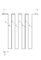
- FIG. 1 is an external view of the thermoelectric conversion module 1 according to the first embodiment of the present invention.
- FIG. 2 is a cross-sectional view of the thermoelectric conversion module 1 along the line L1-L1 shown in FIG.
- FIG. 3 is a cross-sectional view of the thermoelectric conversion module along the L2-L2 line shown in FIG.
- FIG. 4 is a diagram showing a current path in the thermoelectric conversion module shown in FIG.
- thermoelectric conversion module 1 can be arranged in the heat source 2.
- the thermoelectric conversion module 1 has a first edge portion 1H and a second edge portion 1L on a sheet substrate 10 described later.
- the first edge portion 1H and the second edge portion 1L face each other.
- the first edge portion 1H may be located near the heat source 2 when the thermoelectric conversion module 1 is arranged in the heat source 2.
- the second edge portion 1L may be located away from the heat source 2 when the thermoelectric conversion module 1 is arranged in the heat source 2.
- the temperature near the first edge portion 1H can be higher than the temperature near the second edge portion 1L because the first edge portion 1H is located closer to the heat source 2 than the second edge portion 1L. In other words, the temperature near the second edge portion 1L can be lower than the temperature near the first edge portion 1H.
- the first direction A1 is the direction in which the first edge portion 1H and the second edge portion 1L face each other. In the present embodiment, it is assumed that the first direction A1 is the direction from the second edge portion 1L of the thermoelectric conversion module 1 toward the first edge portion 1H.
- the second direction A2 is a direction orthogonal to the first direction A1.
- the second direction A2 does not have to be orthogonal to the first direction A1 as long as it intersects the first direction A1.
- the second direction A2 is the direction from the left side of the paper surface of FIG. 1 toward the right side of the paper surface.
- the third direction A3 is a direction orthogonal to the plane including the first direction A1 and the second direction A2.
- the third direction A3 is the direction from the back side of the paper surface of FIG. 1 toward the front side of the paper surface.
- upper shall refer to the A3 side in the third direction unless otherwise specified.
- downward shall mean the opposite direction side of the third direction A3 unless otherwise specified.
- the shape of the thermoelectric conversion module 1 seen from the third direction A3 is a rectangular shape such as a rectangular shape.
- the shape of the thermoelectric conversion module 1 seen from the third direction A3 may be any shape such as a fan shape.
- the thermoelectric conversion module 1 includes a sheet substrate 10 and thermoelectric conversion elements 21, 22, 23, 24, 25, 26, 27, 28.
- the thermoelectric conversion module 1 includes a connection portion 30, a first electrode 31, and a second electrode 32.
- the connecting portion 30 includes electrodes 41, 42, 43, 44, electrodes 51, 52, 53, a first joining member 61, 62, 63, 64, 65, 66, 67, 68, and a second joining member 71. It has 72,73,74,75,76,77,78 and so on.
- thermoelectric conversion element 20 shows a thermoelectric conversion module 1 including eight thermoelectric conversion elements 20.
- the number of thermoelectric conversion elements 20 included in the thermoelectric conversion module 1 may be any number.
- each of the electrodes 41 to 44 are particularly distinguished, these are collectively referred to as “electrode 40".
- electrode 50 when each of the electrodes 51 to 53 is not particularly distinguished, these are collectively referred to as “electrode 50".
- first joining member 60 when the first joining members 61 to 68 are not particularly distinguished, these are collectively referred to as "first joining member 60”.
- second joining member 70 2 and 3 show a connecting portion 30 having four electrodes 40, three electrodes 50, eight first joining members 60, and eight second joining members 70.
- the number of electrodes 40, the number of electrodes 50, the number of first joining members 60, and the number of second joining members 70 of the connecting portion 30 correspond to the number of thermoelectric conversion elements 20 included in the thermoelectric conversion module 1. May be.
- the sheet substrate 10 as shown in FIG. 1 has an insulating property.
- the sheet substrate 10 may have flexibility.
- the material for forming the sheet substrate 10 is not particularly limited, and any insulating material can be used.
- the shape of the sheet substrate 10 seen from the third direction A3 is a quadrangle such as a rectangle. However, the shape of the sheet substrate 10 seen from the third direction A3 may be any shape such as a fan shape.
- the sheet substrate 10 may be parallel to the surface including the first direction A1 and the second direction A2.
- the sheet substrate 10 has the above-mentioned first edge portion 1H and the above-mentioned second edge portion 1L. As shown in FIGS. 2 and 3, the sheet substrate 10 has a front surface 10A and a back surface 10B. The front surface 10A and the back surface 10B face each other. The surface 10A is a surface of the sheet substrate 10 facing the third direction A3. The back surface 10B is a surface of the sheet substrate 10 facing the opposite direction of the third direction A3.
- the sheet substrate 10 has a substrate 11 and an insulating layer 12.
- the substrate 11 has an insulating property.
- the substrate 11 may have flexibility.
- the material for forming the substrate 11 is not particularly limited, and any material such as polyimide or epoxy glass can be used.
- the shape of the substrate 11 seen from the third direction A3 is a rectangular shape such as a rectangular shape.
- the shape of the substrate 11 seen from the third direction A3 may be any shape such as a fan shape.
- the substrate 11 may be parallel to the plane including the first direction A1 and the second direction A2.
- the substrate 11 has a front surface 11A and a back surface 11B.
- the front surface 11A and the back surface 11B face each other.
- the surface 11A is a surface of the substrate 11 facing the third direction A3.
- the back surface 11B is a surface of the substrate 11 facing the opposite direction of the third direction A3.
- the back surface 11B may correspond to the back surface 10B of the sheet substrate 10.
- the substrate 11 has openings 11a, 11b, 11c, 11d.
- each position of the openings 11a to 11d as seen from the third direction A3 may correspond to each position of the electrodes 41 to 44.
- the substrate 11 has openings 11e, 11f, 11g, 11h.
- each position of the openings 11e to 11g as seen from the third direction A3 may correspond to each position of the electrodes 51 to 53.
- the position of the opening 11h as seen from the third direction A3 may correspond to the position of the second electrode 32.
- the shape of the openings 11a to 11h seen from the third direction A3 is a circular shape. However, the shape of the openings 11a to 11h may be any shape.
- the insulating layer 12 has an insulating property.
- the insulating layer 12 may have flexibility.
- the material for forming the insulating layer 12 is not particularly limited, and any insulating material can be used.
- the insulating layer 12 may be located on the surface 11A of the substrate 11. As shown in FIG. 1, the shape of the insulating layer 12 seen from the third direction A3 is a rectangular shape such as a rectangular shape. However, the shape of the insulating layer 12 seen from the third direction A3 may be any shape such as a fan shape.
- the insulating layer 12 may be parallel to the surface including the first direction A1 and the second direction A2.
- the insulating layer 12 has a front surface 12A and a back surface 12B.
- the front surface 12A and the back surface 12B face each other.
- the surface 12A is a surface of the insulating layer 12 facing the third direction A3.
- the surface 12A may correspond to the surface 10A of the sheet substrate 10.
- the back surface 12B is a surface of the insulating layer 12 facing the opposite direction of the third direction A3.
- the insulating layer 12 has openings 12a, 12b, 12c, 12d. As shown in FIG. 1, each position of the openings 12a to 12d as seen from the third direction A3 may correspond to each position of the electrodes 41 to 44. As shown in FIG. 3, the insulating layer 12 has openings 12e, 12f, 12g, 12h. As shown in FIG. 1, the position of the opening 12e as seen from the third direction A3 may correspond to the position of the first electrode 31. Further, each position of the openings 12f to 12h seen from the third direction A3 may correspond to each position of the electrodes 51 to 53.
- the shape of the openings 12a to 12h seen from the third direction A3 is a circular shape. However, the shape of the openings 12a to 12h may be any shape.
- the thermoelectric conversion element 20 is a p-type thermoelectric conversion element or an n-type thermoelectric conversion element.
- the thermoelectric conversion elements 21, 23, 25, 27 are p-type thermoelectric conversion elements
- the thermoelectric conversion elements 22, 24, 26, 28 are n-type thermoelectric conversion elements.
- the thermoelectric conversion elements 22, 24, 26, and 28, which are n-type thermoelectric conversion elements, are hatched.
- thermoelectric conversion material for forming the thermoelectric conversion element 20 is not particularly limited, and is not particularly limited. Compounds, conductive fibers, composite materials thereof and the like can be used. Above all, it is preferable to use conductive fibers, and it is more preferable to use fibrous carbon nanostructures such as carbon nanotubes (hereinafter, also referred to as “CNT”). This is because if CNTs are used, the mechanical strength of the thermoelectric conversion module 1 of the present invention can be further improved and the weight can be reduced. Further, the CNT is not particularly limited, and a single-walled CNT and / or a multi-walled CNT can be used, but the CNT is preferably a single-walled CNT.
- the single-walled carbon nanotubes are used when CNTs are synthesized by a chemical vapor deposition method (CVD method) by supplying a raw material compound and a carrier gas onto a substrate having a catalyst layer for CNT production on the surface.
- CVD method chemical vapor deposition method
- the manufactured CNT can be used (hereinafter, the CNT manufactured according to such a method may be referred to as "SGCNT").
- SGCNT has a feature that there are many bends.
- CNTs are considered to have high thermal conductivity due to electron transfer, but also have a high effect of lowering thermal conductivity due to phonon vibration.
- SGCNT has more bends than CNTs manufactured according to other general methods, it has a structure in which phonon vibration is less likely to be amplified, and it is possible to suppress a decrease in thermal conductivity due to phonon vibration. .. Therefore, SGCNT can be a more superior material as a thermoelectric conversion material as compared with other general CNTs.
- thermoelectric conversion elements 21 to 28 may be formed including CNTs. With such a configuration, the mechanical strength of the thermoelectric conversion module 1 can be further improved, and the weight of the thermoelectric conversion module 1 can be reduced.
- thermoelectric conversion element 20 extends along the first direction A1.
- the shape of the thermoelectric conversion element 20 seen from the third direction A3 is a long shape such as a rectangular shape. However, the shape of the thermoelectric conversion element 20 seen from the third direction A3 may be any shape such as a fan shape.
- the longitudinal direction of the thermoelectric conversion element 20 is along the first direction A1.
- the longitudinal direction of the thermoelectric conversion element 20 may be parallel to the first direction A1.
- the thermoelectric conversion elements 21 to 28 may have the same shape.
- the cross-sectional shape of the thermoelectric conversion element 20 may be a thin film.
- the thermoelectric conversion element 20 has a first end portion 20H and a second end portion 20L in the first direction A1.
- the first end portion 20H is located toward the first edge portion 1H of the thermoelectric conversion module 1.
- the second end portion 20L is located toward the second edge portion 1L of the thermoelectric conversion module 1.
- the first end portions 20H of the thermoelectric conversion elements 21 to 28 are “first end portion 21H”, “first end portion 22H”, “first end portion 23H", “first end portion 24H”, respectively. It is also described as “first end 25H", “first end 26H", “first end 27H” and “first end 28H”.
- the second end portions 20L of the thermoelectric conversion elements 21 to 28 are “second end portion 21L”, “second end portion 22L”, “second end portion 23L”, “second end portion 24L”, respectively. It is also described as “second end 25L”, “second end 26L”, “second end 27L” and “second end 28L”.
- the positions of the first end portions 21H to 28H in the first direction A1 are different. However, the positions of the first end portions 21H to 28H in the first direction A1 may be the same. Further, in the configuration shown in FIG. 1, the positions of the second end portions 21L to 28L in the first direction A1 are different. However, the positions of the second end portions 21L to 28L in the first direction A1 may be the same.
- the thermoelectric conversion element 20 can generate electricity by utilizing the temperature difference between the first end portion 20H and the second end portion 20L. Specifically, the temperature of the first end portion 20H of the thermoelectric conversion element 20 is such that the first end portion 20H is located closer to the first edge portion 1H than the second end portion 20L, so that the second end portion 20L Can be higher than the temperature of. When the temperature of the first end portion 20H becomes higher than the temperature of the second end portion 20L, a temperature difference may occur between the first end portion 20H and the second end portion 20L. Due to the temperature difference between the first end portion 20H and the second end portion 20L, a temperature gradient may occur in the thermoelectric conversion element 20. The thermoelectric conversion element 20 can generate electric power by generating an electromotive force due to the Zeebeck effect caused by this temperature gradient.
- the plurality of thermoelectric conversion elements 20 are electrically connected in series from the first electrode 31 to the second electrode 32 in the order of the thermoelectric conversion elements 21 to 28 by the connecting portion 30 as described later.
- the connecting portion 30 as described later.
- the plurality of thermoelectric conversion elements 20 By electrically connecting the plurality of thermoelectric conversion elements 20 in series in this way, when the plurality of thermoelectric conversion elements 20 generate electricity, as shown in FIG. 4, one current path is generated in the thermoelectric conversion module 1. obtain.
- each of the currents I21, I22, I23, I24, I25, I26, I27, and I28 is a current flowing through each of the thermoelectric conversion elements 21 to 28.
- the odd-numbered thermoelectric conversion element 20 counting from the first electrode 31 of the plurality of thermoelectric conversion elements 20 electrically connected in series by the connecting portion 30 is located on the side of the surface 10A of the sheet substrate 10. ..
- the odd-numbered thermoelectric conversion element 20 counting from the first electrode 31 is the first thermoelectric conversion element 21, the third thermoelectric conversion element 23, the fifth thermoelectric conversion element 25, and the seventh thermoelectric conversion. It becomes the element 27. That is, the thermoelectric conversion elements 21, 23, 25, 27 are located on the side of the surface 10A of the sheet substrate 10, for example, on the side of the surface 12A of the insulating layer 12.
- the thermoelectric conversion elements 21, 23, 25, 27 are arranged along the second direction A2 on the surface 10A.
- the thermoelectric conversion elements 21, 23, 25, 27 may be arranged with a gap along the second direction A2. The width of the gap may be arbitrary as long as insulation between two thermoelectric conversion elements 20 adjacent to each other in the second direction A2 can be secured.
- thermoelectric conversion element 20 counting from the first electrode 31 among the plurality of thermoelectric conversion elements 20 electrically connected in series by the connecting portion 30 is located on the back surface 10B side of the sheet substrate 10.
- the even-numbered thermoelectric conversion element 20 counting from the first electrode 31 is the second thermoelectric conversion element 22, the fourth thermoelectric conversion element 24, the sixth thermoelectric conversion element 26, and the eighth thermoelectric conversion. It becomes the element 28. That is, the thermoelectric conversion elements 22, 24, 26, and 28 are located on the side of the back surface 10B of the sheet substrate 10, for example, on the side of the back surface 11B of the substrate 11.
- the thermoelectric conversion elements 22, 24, 26, and 28 are arranged along the second direction A2 on the back surface 10B.
- the thermoelectric conversion elements 22, 24, 26, and 28 may be arranged with a gap along the second direction A2. The width of the gap may be arbitrary as long as insulation between two thermoelectric conversion elements 20 adjacent to each other in the second direction A2 can be secured.
- thermoelectric conversion module 1 By locating the thermoelectric conversion element 20 on both the front surface 10A and the back surface 10B of the sheet substrate 10 in this way, the density of the thermoelectric conversion element 20 in the thermoelectric conversion module 1 can be increased. By increasing the density of the thermoelectric conversion element 20 in the thermoelectric conversion module 1, the thermoelectric conversion module 1 can be miniaturized while increasing the generated power.
- thermoelectric conversion module 1 when viewed in a plan view, that is, when viewed from the third direction A3, at least a part of the thermoelectric conversion element 20 located on the surface 10A side of the sheet substrate 10 is the sheet substrate 10. It may overlap with at least a part of the thermoelectric conversion element 20 located on the back surface 10B side. With such a configuration, the thermoelectric conversion module 1 can be miniaturized. However, when viewed from the third direction A3, at least a part of the thermoelectric conversion element 20 located on the side of the front surface 10A of the sheet substrate 10 is at least one of the thermoelectric conversion elements 20 located on the side of the back surface 10B of the sheet substrate 10. It does not have to overlap the parts.
- each of the thermoelectric conversion elements 21 to 28 may be a rectangular shape having substantially the same dimensions. Since the shapes of all the thermoelectric conversion elements 21 to 28 are rectangular with substantially the same dimensions, the thermoelectric conversion elements 20 can be efficiently arranged on each of the front surface 10A and the back surface 10B of the sheet substrate 10. With such a configuration, the thermoelectric conversion module can be miniaturized. However, all the shapes of the thermoelectric conversion elements 21 to 28 may be any shape such as a fan shape as long as they have substantially the same dimensions. Since all the shapes of the thermoelectric conversion elements 21 to 28 have substantially the same dimensions, the thermoelectric conversion elements 20 can be efficiently arranged on each of the front surface 10A and the back surface 10B of the sheet substrate 10.
- thermoelectric conversion elements 21 to 28 have a length along the first direction A1 of each of the thermoelectric conversion elements 21 to 28 so that the electric resistance values of the thermoelectric conversion elements 21 to 28 are substantially the same. It may be configured by adjusting the width along the second direction A2 of each of 28 to 28 and the thickness of the thermoelectric conversion elements 21 to 28 in the third direction A3 of each of the thermoelectric conversion elements 21 to 28.
- the thermoelectric conversion element 20 having a small electric resistance value may cause the thermoelectric conversion module 1. The current is fixed.
- thermoelectric conversion elements 21 to 28 Since the electric resistance values of the thermoelectric conversion elements 21 to 28 are substantially the same, it can be suppressed that the current that can be generated in the thermoelectric conversion module 1 is determined by the thermoelectric conversion element 20 having a small electric resistance value. With such a configuration, the power loss in the thermoelectric conversion module 1 can be reduced.
- Each of the first electrode 31 and the second electrode 32 as shown in FIG. 1 has conductivity.
- the conductive material for forming each of the first electrode 31 and the second electrode 32 is not particularly limited, and any metal such as copper or aluminum can be used.
- a take-out wiring for taking out the electric power generated by the thermoelectric conversion module 1 may be electrically connected to each of the first electrode 31 and the second electrode 32.
- each of the first electrode 31 and the second electrode 32 may be located in the sheet substrate 10, for example, on the surface 11A of the substrate 11.
- the first electrode 31 may be located on the side opposite to the second direction A2 with respect to the electrode 51.
- the width of the gap between the first electrode 31 and the electrode 51 may be arbitrary as long as these two insulations can be secured.
- the second electrode 32 may be located on the second direction A2 side of the electrode 53.
- the width of the gap between the second electrode 32 and the electrode 53 may be arbitrary as long as these two insulations can be secured.
- the first electrode 31 functions as, for example, a negative electrode.
- the first electrode 31 is electrically connected to the end portion of the two ends of the plurality of thermoelectric conversion elements 20 electrically connected in series, which is the negative electrode.
- the first electrode 31 is electrically connected to the second end portion 21L of the thermoelectric conversion element 21.
- at least a part of the first electrode 31 is exposed from the opening 12e of the insulating layer 12.
- At least a part of the first electrode 31 exposed from the opening 12e is electrically connected to the second end 21L of the thermoelectric conversion element 21 by the second joining member 71.
- the second electrode 32 functions as, for example, a positive electrode.
- the second electrode 32 is electrically connected to the end portion of the two ends of the plurality of thermoelectric conversion elements 20 electrically connected in series, which is the positive electrode.
- the second electrode 32 is electrically connected to the second end portion 28L of the thermoelectric conversion element 28.
- at least a part of the second electrode 32 is exposed from the opening 11h of the substrate 11.
- At least a part of the second electrode 32 exposed from the opening 11h is electrically connected to the second end 28L of the thermoelectric conversion element 28 by the second joining member 71.
- the connecting portion 30 connects a plurality of thermoelectric conversion elements 20 from the first electrode 31 to the second electrode 32 at the elongated end portion of each thermoelectric conversion element 20, that is, the first end portion 20H or the second end portion 20L. Electrically connect in series at.
- the connecting portion 30 electrically connects a plurality of thermoelectric conversion elements 20 in series from the first electrode 31 to the second electrode 32 in the order of the thermoelectric conversion elements 21 to 28.
- the connecting portion 30 has a plurality of electrodes 40, a plurality of electrodes 50, a plurality of first joining members 60, and a plurality of second joining members 70.
- the electrode 40 has conductivity.
- the conductive material for forming the electrode 40 is not particularly limited, and any metal such as copper or aluminum can be used.
- the electrode 40 may be located in the sheet substrate 10, for example, on the surface 11A of the substrate 11.
- the electrodes 41 to 44 may be arranged along the second direction A2 with a gap.
- the width of the gap may be arbitrary as long as insulation between two electrodes 40 adjacent to each other in the second direction A2 can be secured.
- the electrodes 40 are formed on the first end portion 20H of the thermoelectric conversion element 20 located on the side of the front surface 10A of the sheet substrate 10 and the first end portion 20H of the thermoelectric conversion element 20 located on the side of the back surface 10B of the sheet substrate 10. It is electrically connected.
- the electrode 41 is electrically connected to the first end portion 21H of the thermoelectric conversion element 21 located on the side of the front surface 10A and the first end portion 22H of the thermoelectric conversion element 22 located on the side of the back surface 10B.
- at least a part of the electrode 41 is exposed from the opening 12a of the insulating layer 12.
- At least a part of the electrode 41 exposed from the opening 12a is electrically connected to the first end 21H of the thermoelectric conversion element 21 by the first joining member 61.
- at least a part of the electrode 41 is exposed from the opening 11a of the substrate 11.
- At least a part of the electrode 41 exposed from the opening 11a is electrically connected to the first end portion 22H of the thermoelectric conversion element 22 by the first joining member 62.
- the position of the electrode 41 in the second direction A2 may be appropriately set according to the position of the thermoelectric conversion element 21 in the second direction A2 and the position of the thermoelectric conversion element 22 in the second direction A2.
- the electrode 42 is electrically connected to the first end portion 23H of the thermoelectric conversion element 23 located on the side of the front surface 10A and the first end portion 24H of the thermoelectric conversion element 24 located on the side of the back surface 10B.
- at least a part of the electrode 42 is exposed from the opening 12b of the insulating layer 12.
- At least a part of the electrode 42 exposed from the opening 12b is electrically connected to the first end portion 23H of the thermoelectric conversion element 23 by the first joining member 63.
- at least a part of the electrode 42 is exposed from the opening 11b of the substrate 11.
- At least a part of the electrode 42 exposed from the opening 11b is electrically connected to the first end portion 24H of the thermoelectric conversion element 24 by the first joining member 64.
- the position of the electrode 42 in the second direction A2 may be appropriately set according to the position of the thermoelectric conversion element 23 in the second direction A2 and the position of the thermoelectric conversion element 24 in the second direction A2.
- the electrode 43 is electrically connected to the first end portion 25H of the thermoelectric conversion element 25 located on the side of the front surface 10A and the first end portion 26H of the thermoelectric conversion element 26 located on the side of the back surface 10B.
- at least a part of the electrode 43 is exposed from the opening 12c of the insulating layer 12.
- At least a part of the electrode 43 exposed from the opening 12c is electrically connected to the first end portion 25H of the thermoelectric conversion element 25 by the first joining member 65.
- at least a part of the electrode 43 is exposed from the opening 11c of the substrate 11.
- At least a part of the electrode 43 exposed from the opening 11c is electrically connected to the first end portion 26H of the thermoelectric conversion element 26 by the first joining member 66.
- the position of the electrode 43 in the second direction A2 may be appropriately set according to the position of the thermoelectric conversion element 25 in the second direction A2 and the position of the thermoelectric conversion element 26 in the second direction A2.
- the electrode 44 is electrically connected to the first end portion 27H of the thermoelectric conversion element 27 located on the side of the front surface 10A and the first end portion 28H of the thermoelectric conversion element 28 located on the side of the back surface 10B.
- at least a part of the electrode 44 is exposed from the opening 12d of the insulating layer 12.
- At least a part of the electrode 44 exposed from the opening 12d is electrically connected to the first end portion 27H of the thermoelectric conversion element 27 by the first joining member 67.
- at least a part of the electrode 44 is exposed from the opening 11d of the substrate 11.
- At least a part of the electrode 44 exposed from the opening 11d is electrically connected to the first end 28H of the thermoelectric conversion element 28 by the first joining member 68.
- the position of the electrode 44 in the second direction A2 may be appropriately set according to the position of the thermoelectric conversion element 27 in the second direction A2 and the position of the thermoelectric conversion element 28 in the second direction A2.
- the electrode 50 has conductivity.
- the conductive material for forming the electrode 50 is not particularly limited, and any metal such as copper or aluminum can be used.
- the electrode 50 may be located in the sheet substrate 10, for example, on the surface 11A of the substrate 11.
- the electrodes 51 to 53 may be arranged along the second direction A2 with a gap between the first electrode 31 and the second electrode 32.
- the width of the gap may be arbitrary as long as insulation between two electrodes 50 adjacent to each other in the second direction A2 can be secured.
- the electrodes 50 are formed on a second end portion 20L of the thermoelectric conversion element 20 located on the side of the front surface 10A of the sheet substrate 10 and a second end portion 20L of the thermoelectric conversion element 20 located on the side of the back surface 10B of the sheet substrate 10. It is electrically connected.
- the electrode 51 is electrically connected to the second end 22L of the thermoelectric conversion element 22 located on the side of the front surface 10A and the second end 23L of the thermoelectric conversion element 23 located on the side of the back surface 10B.
- at least a part of the electrode 51 is exposed from the opening 11e of the substrate 11.
- At least a part of the second electrode exposed from the opening 11e is electrically connected to the second end 22L of the thermoelectric conversion element 22 by the second joining member 72.
- at least a part of the electrode 51 is exposed from the opening 12f of the insulating layer 12.
- At least a part of the electrode 51 exposed from the opening 12f is electrically connected to the second end portion 23L of the thermoelectric conversion element 23 by the second joining member 73.
- the position of the electrode 51 in the second direction A2 may be appropriately set according to the position of the thermoelectric conversion element 22 in the second direction A2 and the position of the thermoelectric conversion element 23 in the second direction A2.
- the electrode 52 is electrically connected to the second end portion 24L of the thermoelectric conversion element 24 located on the side of the front surface 10A and the second end portion 25L of the thermoelectric conversion element 25 located on the side of the back surface 10B.
- the electrode 52 is exposed from the opening 11f of the substrate 11. At least a part of the electrode 52 exposed from the opening 11f is electrically connected to the second end portion 24L of the thermoelectric conversion element 24 by the second joining member 74. Further, at least a part of the electrode 52 is exposed from the opening 12g of the insulating layer 12. At least a part of the electrode 52 exposed from the opening 12g is electrically connected to the second end portion 25L of the thermoelectric conversion element 25 by the second joining member 75.
- the position of the electrode 51 in the second direction A2 may be appropriately set according to the position of the thermoelectric conversion element 24 in the second direction A2 and the position of the thermoelectric conversion element 25 in the second direction A2.
- the electrode 53 is electrically connected to the second end portion 26L of the thermoelectric conversion element 26 located on the side of the front surface 10A and the second end portion 27L of the thermoelectric conversion element 27 located on the side of the back surface 10B.
- at least a part of the electrode 53 is exposed from the opening 11g of the substrate 11.
- At least a part of the electrode 53 exposed from the opening 11g is electrically connected to the second end portion 26L of the thermoelectric conversion element 26 by the second joining member 76.
- at least a part of the electrode 53 is exposed from the opening 12h of the insulating layer 12.
- At least a part of the electrode 53 exposed from the opening 12h is electrically connected to the second end portion 27L of the thermoelectric conversion element 27 by the second joining member 77.
- the first joining member 60 has conductivity.
- the first joining member 60 may be formed of any member such as silver paste or solder.
- the first joining member 61 electrically connects the electrode 41 and the first end portion 21H of the thermoelectric conversion element 21 located on the side of the surface 10A of the sheet substrate 10. For example, as shown in FIG. 2, at least a part of the first joining member 61 is located in the opening 12a of the insulating layer 12. The first joining member 61 electrically connects the electrode 41 and the first end portion 21H of the thermoelectric conversion element 21 via the opening 12a. As shown in FIG. 1, the first joining member 61 may extend from the opening 12a to the first end 21H of the thermoelectric conversion element 21.
- the first joining member 62 electrically connects the electrode 41 and the first end portion 22H of the thermoelectric conversion element 22 located on the back surface 10B side of the sheet substrate 10. For example, as shown in FIG. 2, at least a part of the first joining member 62 is located in the opening 11a of the substrate 11. The first joining member 62 electrically connects the electrode 41 and the first end portion 22H of the thermoelectric conversion element 22 via the opening 11a. As shown in FIG. 1, the first joining member 62 may extend from the opening 11a to the first end 22H of the thermoelectric conversion element 22.
- the first joining member 63 electrically connects the electrode 42 and the first end portion 22H of the thermoelectric conversion element 23 located on the side of the surface 10A of the sheet substrate 10. For example, as shown in FIG. 2, at least a part of the first joining member 63 is located in the opening 12b of the insulating layer 12. The first joining member 63 electrically connects the electrode 42 and the first end portion 23H of the thermoelectric conversion element 23 via the opening 12a. As shown in FIG. 1, the first joining member 63 may extend from the opening 12a to the first end 23H of the thermoelectric conversion element 23.
- the first joining member 64 electrically connects the electrode 42 and the first end portion 24H of the thermoelectric conversion element 24 located on the back surface 10B side of the sheet substrate 10. For example, as shown in FIG. 2, at least a part of the first joining member 64 is located in the opening 11b of the substrate 11.
- the first joining member 64 electrically connects the electrode 42 and the first end portion 24H of the thermoelectric conversion element 24 via the opening 11b. As shown in FIG. 1, the first joining member 64 may extend from the opening 11a to the first end 24H of the thermoelectric conversion element 24.
- the first joining member 65 electrically connects the electrode 43 and the first end portion 25H of the thermoelectric conversion element 25 located on the side of the surface 10A of the sheet substrate 10. For example, as shown in FIG. 2, at least a part of the first joining member 65 is located in the opening 12c of the insulating layer 12.
- the first joining member 64 electrically connects the electrode 43 and the first end portion 25H of the thermoelectric conversion element 25 via the opening 12c. As shown in FIG. 1, the first joining member 65 may extend from the opening 12c to the first end 25H of the thermoelectric conversion element 25.
- the first joining member 66 electrically connects the electrode 43 and the first end portion 26H of the thermoelectric conversion element 26 located on the back surface 10B side of the sheet substrate 10. For example, as shown in FIG. 2, at least a part of the first joining member 65 is located in the opening 11c of the substrate 11. The first joining member 65 electrically connects the electrode 43 and the first end portion 26H of the thermoelectric conversion element 26 via the opening 11c. As shown in FIG. 1, the first joining member 66 may extend from the opening 11c to the first end 26H of the thermoelectric conversion element 26.
- the first joining member 67 electrically connects the electrode 44 and the first end portion 27H of the thermoelectric conversion element 27 located on the side of the surface 10A of the sheet substrate 10. For example, as shown in FIG. 2, at least a part of the first joining member 67 is located in the opening 12d of the insulating layer 12. The first joining member 67 electrically connects the electrode 44 and the first end portion 27H of the thermoelectric conversion element 27 via the opening 12d. As shown in FIG. 1, the first joining member 67 may extend from the opening 12d to the first end 27H of the thermoelectric conversion element 27.
- the first joining member 68 electrically connects the electrode 44 and the first end portion 28H of the thermoelectric conversion element 28 located on the back surface 10B side of the sheet substrate 10. For example, as shown in FIG. 2, at least a part of the first joining member 68 is located in the opening 11d of the substrate 11. The first joining member 68 electrically connects the electrode 44 and the first end portion 28H of the thermoelectric conversion element 28 via the opening 11d. As shown in FIG. 1, the first joining member 68 may extend from the opening 11d to the first end 28H of the thermoelectric conversion element 28.
- the second joining member 70 has conductivity.
- the second joining member 70 may be formed of any member such as silver paste or solder.
- the second joining member 71 electrically connects the first electrode 31 and the second end portion 21L of the thermoelectric conversion element 21 located on the surface 10A side of the sheet substrate 10. For example, as shown in FIG. 3, at least a part of the second joining member 71 is located in the opening 12e of the insulating layer 12. The second joining member 71 electrically connects the first electrode 31 and the second end portion 21L of the thermoelectric conversion element 21 via the opening 12e. As shown in FIG. 1, the second joining member 71 may extend from the opening 12e to the second end 21L of the thermoelectric conversion element 21.
- the second joining member 72 electrically connects the electrode 51 and the second end portion 22L of the thermoelectric conversion element 22 located on the back surface 10B side of the sheet substrate 10. For example, as shown in FIG. 3, at least a part of the second joining member 72 is located in the opening 11e of the substrate 11.
- the second joining member 72 electrically connects the electrode 51 and the second end portion 22L of the thermoelectric conversion element 22 via the opening 11e. As shown in FIG. 1, the second joining member 72 may extend from the opening 11e to the second end 22L of the thermoelectric conversion element 22.
- the second joining member 73 electrically connects the electrode 51 and the second end portion 23L of the thermoelectric conversion element 23 located on the side of the surface 10A of the sheet substrate 10. For example, as shown in FIG. 3, at least a part of the second joining member 73 is located in the opening 12f of the insulating layer 12. The second joining member 73 electrically connects the electrode 51 and the second end portion 23L of the thermoelectric conversion element 23 via the opening 12f. As shown in FIG. 1, the second joining member 73 may extend from the opening 12f to the second end 23L of the thermoelectric conversion element 23.
- the second joining member 74 electrically connects the electrode 52 and the second end portion 24L of the thermoelectric conversion element 24 located on the back surface 10B side of the sheet substrate 10. For example, as shown in FIG. 3, at least a part of the second joining member 74 is located in the opening 11f of the substrate 11. The second joining member 74 electrically connects the electrode 52 and the second end portion 24L of the thermoelectric conversion element 24 via the opening 11f. As shown in FIG. 1, the second joining member 74 may extend from the opening 11f to the second end 24L of the thermoelectric conversion element 24.
- the second joining member 75 electrically connects the electrode 52 and the second end portion 25L of the thermoelectric conversion element 25 located on the side of the surface 10A of the sheet substrate 10. For example, as shown in FIG. 3, at least a part of the second joining member 75 is located in the opening 12g of the insulating layer 12. The second joining member 75 electrically connects the electrode 52 and the second end portion 25L of the thermoelectric conversion element 25 via the opening 12g. As shown in FIG. 1, the second joining member 75 may extend from the opening 12g to the second end 25L of the thermoelectric conversion element 25.
- the second joining member 76 electrically connects the electrode 53 and the second end portion 26L of the thermoelectric conversion element 26 located on the back surface 10B side of the sheet substrate 10. For example, as shown in FIG. 3, at least a part of the second joining member 76 is located in the opening 11g of the substrate 11. The second joining member 76 electrically connects the electrode 53 and the second end portion 26L of the thermoelectric conversion element 26 via the opening 11g. As shown in FIG. 1, the second joining member 76 may extend from the opening 11g to the second end 26L of the thermoelectric conversion element 26.
- the second joining member 77 electrically connects the electrode 53 and the second end portion 27L of the thermoelectric conversion element 27 located on the side of the surface 10A of the sheet substrate 10. For example, as shown in FIG. 3, at least a part of the second joining member 77 is located in the opening 12h of the insulating layer 12. The second joining member 77 electrically connects the electrode 53 and the second end portion 27L of the thermoelectric conversion element 27 via the opening 12h. As shown in FIG. 1, the second joining member 77 may extend from the opening 12h to the second end 27L of the thermoelectric conversion element 27.
- the second joining member 78 electrically connects the second electrode 32 and the second end portion 28L of the thermoelectric conversion element 28 located on the back surface 10B side of the sheet substrate 10. For example, as shown in FIG. 3, at least a part of the second joining member 78 is located in the opening 11h of the substrate 11.
- the second joining member 78 electrically connects the second electrode 32 and the second end portion 28L of the thermoelectric conversion element 28 via the opening 11h. As shown in FIG. 1, the second joining member 78 may extend from the opening 11h to the second end 28L of the thermoelectric conversion element 28.
- thermoelectric conversion module 1 the thermoelectric conversion element 20 is located on both the front surface 10A and the back surface 10B of the sheet substrate 10. With such a configuration, the thermoelectric conversion module 1 can be miniaturized while the density of the thermoelectric conversion element 20 in the thermoelectric conversion module 1 is increased. Therefore, according to the present embodiment, a miniaturized thermoelectric conversion module 1 can be provided while increasing the generated power.
- FIG. 5 is an external view of the thermoelectric conversion module 101 according to a modified example of the first embodiment of the present invention.
- FIG. 6 is a cross-sectional view of the thermoelectric conversion module 101 along the L3-L3 line shown in FIG.
- FIG. 7 is a cross-sectional view of the thermoelectric conversion module 101 along the L4-L4 line shown in FIG.
- thermoelectric conversion module 101 when viewed from the third direction A3, the entire thermoelectric conversion element 20 located on the front surface 10A side of the sheet substrate 10 and the thermoelectric conversion element 20 located on the back surface 10B side of the sheet substrate 10 It overlaps with the entire conversion element 20. With such a configuration, the thermoelectric conversion module 101 can be miniaturized while the density of the thermoelectric conversion element 20 in the thermoelectric conversion module 101 is further increased.
- the respective positions of the openings 12a to 12d of the insulating layer 12 and the respective positions of the openings 11a to 11d of the substrate 11 are It may be the same. Further, when viewed from the third direction A3, the positions of the first joining members 61, 63, 65, 67 and the positions of the second joining members 71, 73, 75, 77 are the same. good.
- thermoelectric conversion module 101 according to the modified example of the first embodiment are the same as those of the thermoelectric conversion module 1 according to the first embodiment.
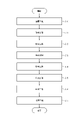
- FIG. 8 is a flowchart showing a manufacturing method of the thermoelectric conversion module 1 shown in FIG.
- the method for manufacturing the thermoelectric conversion module 1 includes an arrangement step S10, a forming step S11, S12, S13, S14, S15, S16, and a connection step S17.
- the manufacturing method of the thermoelectric conversion module 1 according to the present embodiment is not limited to the manufacturing method described below. 11 to 14 correspond to the cross-sectional views shown in FIG.
- the arrangement step S10 is a step of arranging the metal foil 33 on the substrate 11 as shown in FIG.
- the metal leaf 33 may be arranged on the surface 11A of the substrate 11.
- the metal leaf 33 may be adhered to the surface 11A of the substrate 11 by any adhesive having thermal conductivity.
- the metal leaf 33 may be formed on the surface 11A of the substrate 11 by any film forming method such as thin film deposition, sputtering, or plating method.
- the metal foil 33 can become the first electrode 31, the second electrode 32, the electrode 40, and the electrode 50 through the forming step S11 and the like described later.
- the metal leaf 33 may be any metal leaf such as copper or aluminum.
- the forming step S11 is a step of forming the electrode layer 34 as shown in FIG. 10 by patterning the metal foil 33.
- the electrode layer 34 has a first electrode 31, a second electrode 32, an electrode 40, and an electrode 50.
- the electrode layer 34 is formed only on the surface 11A of the substrate 11.
- the electrode layer 34 may be formed on at least one of the front surface 11A and the back surface 11B of the substrate 11.
- the forming step S12 is a step of forming the openings 11a, 11b, 11c, 11d of the substrate 11 as shown in FIG. 11 and forming the openings 11e, 11f, 11g, 11h of the substrate 11 as shown in FIG. be.
- the openings 11a to 11h may be formed by any heating laser.
- the forming step S13 is a step of forming the insulating layer 12 on the electrode layer 34 formed on the substrate 11, as shown in FIG.
- the insulating layer 12 may be formed on the substrate 11 and the electrode layer 34.
- the insulating layer 12 may be formed by applying an insulating material to the electrode layer 34.
- the sheet substrate 10 includes a substrate 11 and an insulating layer 12.
- ⁇ Formation step S14> In the forming step S14, as shown in FIG. 13, the openings 12a, 12b, 12c, 12d of the insulating layer 12 are formed, and the openings 12e, 12f, 12g, 12h of the insulating layer 12 as shown in FIG. 3 are formed. It is a process.
- the openings 12a-12h may be formed by any heating laser.
- the forming step S15 is a step of forming a thermoelectric conversion element layer on the insulating layer 12 and on the surface on which the electrode layer 34 is not formed on the substrate 11.
- the forming step S15 may be a step of forming a thermoelectric conversion element layer on each of the front surface 10A and the back surface 10B of the sheet substrate 10.
- the thermoelectric conversion element layer is a layer formed including CNT.
- the thermoelectric conversion element layer can become the thermoelectric conversion element 20 after undergoing the formation step S16 or the like described later.
- the mechanical strength of the thermoelectric conversion module 1 can be further improved and the weight can be reduced. Since the thermoelectric conversion element layer is formed to include CNTs, the thermoelectric conversion module 1 having further improved mechanical strength and reduced weight can be manufactured.
- the thermoelectric conversion element layer is a CNT sheet 29P and a CNT sheet 29N (carbon nanotube sheet) as shown in FIG.
- the CNT sheets 29P and 29N are formed to include CNTs.
- the CNT sheet 29P is arranged on the front surface 10A of the sheet substrate 10, for example, the front surface 12A of the insulating layer 12, and the CNT sheet 29N is arranged on the back surface 10B of the sheet substrate 10, for example, the back surface 11B of the substrate 11. It becomes a process.
- the CNT sheet 29P is a p-type CNT sheet.
- the CNT sheet 29P may be adhered to the surface 10A of the sheet substrate 10 by any adhesive sheet such as epoxy resin.
- the CNT sheet 29P can become the thermoelectric conversion elements 21, 23, 25, 27 after undergoing the formation step S16 and the like described later.
- the CNT sheet 29N is an n-type CNT sheet.
- the CNT sheet 29N may be adhered to the back surface 10B of the sheet substrate 10 by any adhesive sheet such as epoxy resin.
- the CNT sheet 29N can become the thermoelectric conversion elements 22, 24, 26, 28 after undergoing the formation step S16 and the like described later.
- CNT sheet 29 when the CNT sheet 29P and the CNT sheet 29N are not particularly distinguished, these are collectively referred to as "CNT sheet 29".
- the thickness of the CNT sheet 29 in the third direction A3 may be about 50 [ ⁇ m].
- the electrical characteristics of the thermoelectric conversion element 20 can be exhibited.
- the amount of power generation of the thermoelectric conversion element 20 can be secured to some extent.
- the CNT coating film formed by the coating method using the CNT dispersion liquid may be arranged on the insulating layer 12 or the substrate 11.
- the CNT coating film there are problems that the conductivity of the CNT coating film is lowered and the independence of the CNT coating film is lowered due to the aggregation of CNTs in the process of drying the CNT dispersion liquid. Can occur.
- the CNT sheet 29 is not particularly limited, and the one described in Japanese Patent Application No. 2018-065290 can be used.
- the CNT sheet 29 may include a bundle in which a plurality of single-walled CNTs are intertwined.
- the thickness of the bundle may be 1 [ ⁇ m] or less.
- the fluffing of the cut surface of the thermoelectric conversion element 20 by the laser in the forming step S16 described later can be reduced. By reducing the fluffing of the thermoelectric conversion element 20, it is possible to suppress the occurrence of a short circuit due to the fluffing of the thermoelectric conversion element 20.
- a sheet to be a cover may be arranged on the CNT sheet 29 in order to reduce the damage caused by the laser in the forming step S16 described later, or the CNT sheet 29 may be arranged.
- a resin material may be applied to the.
- thermoelectric conversion element forming step is a step of cutting the thermoelectric conversion element layer, that is, the CNT sheet 29 along the first direction A1 to form a plurality of thermoelectric conversion elements 20 arranged in the second direction A2.
- the gap s1 as shown in FIG. 15 is formed.
- Two thermoelectric conversion elements 20 adjacent to each other in the second direction A2 can be partitioned by the gap s1.
- the forming step S16 may be carried out using a laser.
- each of the CNT sheets 29P and 29N may be cut along the first direction A1 by the laser.
- the laser may be irradiated toward the CNT sheet 29P from the third direction A3 side. Further, the laser may be irradiated toward the CNT sheet 29N from the opposite direction side of the third direction A3.
- the gap s1 as shown in FIG. 15 can be formed.
- the CNT sheet 29 may be cut along the first direction A1 by a UV (UltraViolet) laser, a nanosecond laser, or a femtosecond laser.
- the laser used in the forming step S16 is not limited to these lasers.
- only the CNT sheet P can be cut when the CNT sheet 29P is irradiated from the third direction A3 side, and when the CNT sheet 29N is irradiated from the opposite side of the third direction A3. Any laser capable of cutting only the CNT sheet N may be used.
- the UV laser may scan the portion of the CNT sheet 29 corresponding to the gap s1 ten to several tens of times along the first direction A1.
- the thermal conductivity in the in-plane direction of the CNT sheet 29 can be about 100 times the thermal conductivity in the thickness direction of the CNT sheet 29.
- the thermal conductivity of the CNT sheet 29 in the second direction A2 can be about 100 times the thermal conductivity of the CNT sheet 29 in the third direction A3. Therefore, when a heating laser such as a YAG (Yttrium Aluminum Garnet) laser is used in the forming step S16, when the CNT sheet 29 is cut along the first direction A1 by the heating laser, the gap s1 becomes the second direction A2. May spread in.
- the heating laser is used in the forming step S16 when the thickness of the CNT sheet 29 in the third direction A3 is about 50 [ ⁇ m], the gap s1 may widen by about 5 mm in the second direction A2. ..
- thermoelectric conversion module 1 can be miniaturized.
- the spot diameter of the UV laser can be smaller than the spot diameter of other lasers.
- the spot diameter of the UV laser can be about 8 [ ⁇ m].
- the small spot diameter of the UV laser can focus the UV laser on the CNT sheet 29.
- the width of the gap s1 in the second direction A2 can be about 0.05 [mm] to 0.1 [mm].
- the forming step S16 By using a laser in the forming step S16, patterning of the CNT sheet 29 by the laser can be performed by computer control. With such a configuration, the forming step S16 can be simplified.
- connection step S17 the end portion of each thermoelectric conversion element 20, that is, the first end portion 20H or the second end portion 20L is electrically connected by the connection portion 30 so that all of the plurality of thermoelectric conversion elements 20 are electrically connected in series. It is a process of connecting to the target.
- connection step S17 is a step of applying the silver paste.
- connection step S17 from each of the openings 12a to 12d of the insulating layer 12 as shown in FIG. 1, the first end portion 21H of the thermoelectric conversion element 21, the first end portion 23H of the thermoelectric conversion element 23, and the thermoelectric conversion element 25
- the silver paste is applied along the first direction A1 to each of the first end portion 25H of the above and the first end portion 27H of the thermoelectric conversion element 27.
- a part of this silver paste is filled in each of the openings 12a to 12d and electrically connected to each of the electrodes 41 to 44. After drying, these silver pastes can become the first joining members 61, 63, 65, 67.
- connection step S17 from each of the openings 11a to 11d of the substrate 11 as shown in FIG. 1, the first end portion 22H of the thermoelectric conversion element 22, the first end portion 24H of the thermoelectric conversion element 24, and the thermoelectric conversion element 26
- the silver paste is applied along the first direction A1 to each of the first end portion 26H and the first end portion 28H of the thermoelectric conversion element 28.
- a part of this silver paste is filled in the openings 11a to 11d and electrically connected to each of the electrodes 41 to 44. After drying, these silver pastes can become the first joining members 62, 64, 66, 68.
- connection step S17 the silver paste is applied along the first direction A1 from the opening 12e of the insulating layer 12 as shown in FIG. 1 to the second end 21L of the thermoelectric conversion element 21. A part of this silver paste is filled in the opening 12e and electrically connected to the first electrode 31. This silver paste can become the second joining member 71 after drying.
- connection step S17 from each of the openings 12f and 12g of the insulating layer 12 as shown in FIG. 1 to each of the second end 23L of the thermoelectric conversion element 23 and the second end 25L of the thermoelectric conversion element 25.
- the silver paste is applied along one direction A1. A part of these silver pastes is filled in each of the openings 12f and 12g and electrically connected to each of the electrodes 51 and 52. After drying, these silver pastes can become the second joining members 73,75.
- connection step S17 from each of the openings 11e to 11g of the substrate 11 as shown in FIG. 1, the second end portion 22L of the thermoelectric conversion element 22, the second end portion 24L of the thermoelectric conversion element 24, and the thermoelectric conversion element 26
- the silver paste is applied along the first direction A1 up to each of the second end portions 26L. A part of these silver pastes is filled in each of the openings 11e to 11g and electrically connected to each of the electrodes 51 to 53. After drying, these silver pastes can become the second joining members 72,74,76.
- connection step S17 the silver paste is applied along the first direction A1 from the opening 11h of the substrate 11 as shown in FIG. 1 to the second end 28L of the thermoelectric conversion element 28. A part of this silver paste is filled in the opening 11h and electrically connected to the second electrode 32. This silver paste can become the second joining member 78 after drying.
- the CNT sheet 29 can be cut along the first direction A1 by a UV laser, a nanosecond laser, or a femtosecond laser in the forming step S16.
- the gap s1 as shown in FIG. 15 can be suppressed from expanding in the second direction A2.
- the density of the thermoelectric conversion element 20 in the thermoelectric conversion module 1 can be increased, and the thermoelectric conversion module 1 can be miniaturized.
- thermoelectric conversion module 1 has been described as having the electrode layer 34 only on the surface 11A of the substrate 11. Further, the thermoelectric conversion element 20 located on the surface 10A side of the sheet substrate 10 is electrically connected to the thermoelectric conversion element 20 located on the back surface 10B side of the sheet substrate 10 via the substrate 11, the electrode layer 34 and the insulating layer 12. It was explained as being connected. However, the thermoelectric conversion module 1 may be provided with electrode layers 34 on both the front surface 11A and the back surface 11B of the substrate 11. In this case, the thermoelectric conversion module 1 may include an insulating layer 12 on each of the electrode layers 34 on both sides of the front surface 11A and the back surface 11B of the substrate 11.
- thermoelectric conversion element 20 located on the side of the front surface 10A of the sheet substrate 10 is located on the side of the back surface 10B of the sheet substrate 10 via the insulating layer 12, the electrode layer 34, the substrate 11, the electrode layer 34, and the insulating layer 12. It may be electrically connected to the thermoelectric conversion element 20 located at.
- FIG. 16 is an external view of the thermoelectric conversion module 201 according to the second embodiment of the present invention.
- FIG. 17 is a cross-sectional view of the thermoelectric conversion module 201 along the L5-L5 line shown in FIG.
- FIG. 18 is a cross-sectional view of the thermoelectric conversion module 201 along the L6-L6 line shown in FIG.
- FIG. 19 is a diagram showing the electrode layer 234 shown in FIG. The configuration shown in FIG. 19 corresponds to the configuration after carrying out the formation step S11 of the electrode layer 234 described later.
- FIG. 20 is a diagram showing a current path in the thermoelectric conversion module 101 shown in FIG.
- the thermoelectric conversion module 201 can be arranged in the heat source 2 as in the first embodiment.
- the thermoelectric conversion module 201 has a first edge portion 201H and a second edge portion 201L on the sheet substrate 210 described later.
- the first edge portion 201H and the second edge portion 201L face each other.
- the first edge portion 201H may be located near the heat source 2 when the thermoelectric conversion module 201 is arranged in the heat source 2, similarly to the first edge portion 1H as shown in FIG.
- the second edge portion 201L may be located away from the heat source 2 when the thermoelectric conversion module 201 is arranged in the heat source 2, similarly to the second edge portion 1L as shown in FIG.
- the temperature near the first edge portion 201H can be higher than the temperature near the second edge portion 201L, similarly to the first edge portion 1H as shown in FIG. In other words, the temperature near the second edge portion 201L can be lower than the temperature near the first edge portion 201H.
- the first direction A1, the second direction A2, and the third direction A3 can be adopted as in the first embodiment.
- the first direction A1 is the direction in which the first edge portion 201H and the second edge portion 201L face each other. It is assumed that the first direction A1 is the direction from the second edge portion 201L toward the first edge portion 201H.
- the third direction A3 is assumed to be a direction from the back side of the paper surface of FIG. 16 toward the front side of the paper surface.
- the shape of the thermoelectric conversion module 201 seen from the third direction A3 is a rectangular shape such as a rectangular shape.
- the shape of the thermoelectric conversion module 201 seen from the third direction A3 may be any shape such as a fan shape.
- the thermoelectric conversion module 201 includes a sheet substrate 210 and thermoelectric conversion elements 221,222,223,224,225,226,227,228.
- the thermoelectric conversion module 201 includes a connection portion 230, a first electrode 251 and a second electrode 248. As shown in FIGS.
- connection portion 230 is first joined to the electrodes 241,242,243,244,245,246,247 and the electrodes 252,253,254,255,256,257,258.
- thermoelectric conversion element 220 when each of the thermoelectric conversion elements 221 to 228 is not particularly distinguished, these are collectively referred to as "thermoelectric conversion element 220".
- FIG. 13 shows a thermoelectric conversion module 201 including eight thermoelectric conversion elements 220.
- the number of thermoelectric conversion elements 220 included in the thermoelectric conversion module 201 may be any number.
- FIG. 19 shows a connection 230 having eight electrodes 240, eight electrodes 250, and seven wires 280.
- the number of electrodes 240, the number of electrodes 250, and the number of wirings 280 of the connection portion 230 may correspond to the number of thermoelectric conversion elements 220 included in the thermoelectric conversion module 201.
- FIG. 16 shows a thermoelectric conversion module 201 including eight first joining members 260 and eight second joining members 270.
- the number of the first joining member 260 and the number of the second joining members 270 included in the thermoelectric conversion module 201 may correspond to the number of the thermoelectric conversion elements 220 included in the thermoelectric conversion module 201.
- the sheet substrate 210 has an insulating property.
- the sheet substrate 210 may have flexibility.
- the material for forming the sheet substrate 210 is not particularly limited, and any insulating material can be used.
- the shape of the sheet substrate 210 seen from the third direction A3 is a four-sided rectangular shape such as a rectangular shape. However, the shape of the sheet substrate 210 seen from the third direction A3 may be any shape such as a fan shape.
- the sheet substrate 210 may be parallel to the surface including the first direction A1 and the second direction A2.
- the sheet substrate 210 has the above-mentioned first edge portion 201H and the above-mentioned second edge portion 201L. As shown in FIG. 17, the sheet substrate 210 has a front surface 210A and a back surface 210B. The front surface 210A and the back surface 210B face each other. The surface 210A is a surface of the sheet substrate 210 facing the third direction A3. The back surface 210B is a surface of the sheet substrate 210 facing in the opposite direction of the third direction A3.
- the sheet substrate 210 has a substrate 211 and an insulating layer 212.
- the substrate 211 has an insulating property.
- the substrate 211 may have flexibility.
- the material of the substrate 211 may be the same as the material of the substrate 11 as shown in FIG.
- the shape of the substrate 11 seen from the third direction A3 is a rectangular shape such as a rectangular shape.
- the shape of the substrate 11 seen from the third direction A3 may be any shape such as a fan shape.
- the substrate 211 may be parallel to the plane including the first direction A1 and the second direction A2.
- the substrate 211 has a front surface 211A and a back surface 211B.
- the front surface 211A and the back surface 211B face each other.
- the surface 211A is a surface of the substrate 211 facing the third direction A3.
- the back surface 211B is a surface of the substrate 211 that faces the opposite direction of the third direction A3.
- the back surface 211B may correspond to the back surface 210B of the sheet substrate 210.
- the substrate 211 has openings 211a, 211b, 211c, 211d.
- the positions of the openings 211a to 211d as seen from the third direction A3 may correspond to the positions of the electrodes 242, 244, 246 and the second electrode 248.
- the substrate 211 has openings 211e, 211f, 211g, 211h.
- each position of the openings 211e to 211h seen from the third direction A3 may correspond to each position of the electrodes 252, 254, 256, 258.
- the shape of the openings 211a to 211h seen from the third direction A3 is a circular shape. However, the shape of the openings 211a to 211h may be any shape.
- the insulating layer 212 has an insulating property.
- the insulating layer 212 may have flexibility.
- the material of the insulating layer 212 may be the same as the material of the insulating layer 12 as shown in FIG.
- the shape of the insulating layer 212 as seen from the third direction A3 is a rectangular shape such as a rectangular shape. However, the shape of the insulating layer 212 as seen from the third direction A3 may be any shape such as a fan shape.
- the insulating layer 212 may be parallel to the surface including the first direction A1 and the second direction A2.
- the insulating layer 212 has a front surface 212A and a back surface 212B.
- the front surface 212A and the back surface 212B face each other.
- the surface 212A is a surface of the insulating layer 212 facing the third direction A3.
- the surface 212A may correspond to the surface 210A of the sheet substrate 210.
- the back surface 212B is a surface of the insulating layer 212 facing the opposite direction of the third direction A3.
- the insulating layer 212 has openings 212a, 212b, 212c, 212d. As shown in FIG. 16, each position of the openings 212a to 212d seen from the third direction A3 may correspond to each position of the electrodes 241,243,245,247. As shown in FIG. 18, the insulating layer 212 has openings 212e, 212f, 212g, 212h. As shown in FIG. 16, each position of the openings 212e to 212h seen from the third direction A3 may correspond to each position of the first electrode 251 and the electrodes 253, 255, 257.
- the shape of the openings 212a to 212h seen from the third direction A3 is a circular shape. However, the shape of the openings 212a to 212h may be any shape.
- thermoelectric conversion elements 221 to 228 are p-type thermoelectric conversion elements. That is, in the thermoelectric conversion element 220 located on both sides of the front surface 210A and the back surface 210B of the sheet substrate 210 as described later, the thermoelectric conversion element 220 located on the side of the front surface 210A and the thermoelectric conversion element 220 located on the side of the back surface 210B. All are p-type thermoelectric conversion elements. However, all of the thermoelectric conversion elements 221 to 228 may be n-type thermoelectric conversion elements.
- the thermoelectric conversion material for forming the thermoelectric conversion element 220 is not particularly limited, and the thermoelectric conversion material described above in the first embodiment can be used.
- thermoelectric conversion module 201 depending on the thermoelectric conversion material forming the thermoelectric conversion element 220, one of the p-type thermoelectric conversion element and the n-type thermoelectric conversion element may have higher durability than the other. Since all of the plurality of thermoelectric conversion elements 220 included in the thermoelectric conversion module 201 are p-type thermoelectric conversion elements or n-type thermoelectric conversion elements, the thermoelectric conversion module 201 can be excellent in durability.
- thermoelectric conversion elements 221 to 228 may be formed including CNTs as described above in the first embodiment.
- the thermoelectric conversion material is an organic material
- oxidation of the thermoelectric conversion element 220 by oxygen, moisture, or the like in the atmosphere may be the main cause of deterioration of the characteristics of the thermoelectric conversion element 220.
- the p-type thermoelectric conversion element is more susceptible to oxidation due to oxygen and moisture in the atmosphere than the p-type thermoelectric conversion element, so that the p-type thermoelectric conversion element is more susceptible than the n-type thermoelectric conversion element. It can be more durable.
- the thermoelectric conversion module 201 can be excellent in durability because all of the plurality of thermoelectric conversion elements 220 included in the thermoelectric conversion module 201 are p-type thermoelectric conversion elements. ..
- the thermoelectric conversion element 220 extends along the first direction A1.
- the shape of the thermoelectric conversion element 220 seen from the third direction A3 is a long shape such as a rectangular shape. However, the shape of the thermoelectric conversion element 220 seen from the third direction A3 may be any shape such as a fan shape.
- the longitudinal direction of the thermoelectric conversion element 220 is along the first direction A1.
- the longitudinal direction of the thermoelectric conversion element 220 may be parallel to the first direction A1.
- the thermoelectric conversion elements 221 to 228 may have the same shape.
- the thermoelectric conversion element 220 has a first end portion 220H and a second end portion 220L in the first direction A1, similarly to the thermoelectric conversion element 20 as shown in FIG.
- the first end portion 220H is located toward the first edge portion 201H of the thermoelectric conversion module 201.
- the second end portion 220L is located toward the second edge portion 201L of the thermoelectric conversion module 201.
- the first end 220H of the thermoelectric conversion elements 221 to 228 are “first end 221H”, “first end 222H”, “first end 223H”, “first end 224H", respectively. It is also described as “first end portion 225H”, “first end portion 226H”, “first end portion 227H", and “first end portion 228H”.
- the second end 220L of the thermoelectric conversion elements 221 to 228 are “second end 221L”, “second end 222L”, “second end 223L”, “second end 224L”, respectively. It is also described as “second end portion 225L”, “second end portion 226L”, “second end portion 227L”, and “second end portion 228L”.
- the positions of the first end portions 221H to 228H in the first direction A1 are different. However, the positions of the first end portions 221H to 228H in the first direction A1 may be the same. Further, in the configuration shown in FIG. 16, the positions of the second end portions 221L to 228L in the first direction A1 are different. However, the positions of the second end portions 221L to 228L in the first direction A1 may be the same.
- thermoelectric conversion element 220 can generate electricity due to a temperature difference between the first end portion 220H and the second end portion 220L.
- the plurality of thermoelectric conversion elements 220 are electrically connected in series from the first electrode 251 to the second electrode 248 in the order of the thermoelectric conversion elements 221 to 228 by the connecting portion 230.
- the plurality of thermoelectric conversion elements 220 By electrically connecting the plurality of thermoelectric conversion elements 220 in series in this way, when the plurality of thermoelectric conversion elements 220 generate electricity, as shown in FIG. 20, one current path is generated in the thermoelectric conversion module 201. obtain.
- each of the currents I221, I222, I223, I224, I225, I226, I227, and I228 is the current flowing through each of the thermoelectric conversion elements 221,222, 223, 224, 225, 226, 227, and 228.
- each of the currents I281,282,283,284,285,286,287 is a current flowing through each of the wirings 281 to 287 described later.
- the odd-numbered thermoelectric conversion element 220 counted from the first electrode 251 of the plurality of thermoelectric conversion elements 220 electrically connected in series by the connecting portion 230 is located on the side of the surface 210A of the sheet substrate 210. ..
- the odd-numbered thermoelectric conversion element 220 counted from the first electrode 251 is the first thermoelectric conversion element 221, the third thermoelectric conversion element 223, the fifth thermoelectric conversion element 225, and the seventh thermoelectric conversion. It becomes the element 227. That is, the thermoelectric conversion elements 221,223,225,227 are located on the side of the surface 210A of the sheet substrate 210, for example, on the side of the surface 212A of the insulating layer 212.
- thermoelectric conversion elements 221,223,225,227 are arranged along the second direction A2 on the surface 210A.
- the thermoelectric conversion elements 221,223,225,227 may be arranged with a gap along the second direction A2.
- the width of the gap may be arbitrary as long as insulation between two thermoelectric conversion elements 220 adjacent to each other in the second direction A2 can be secured.
- thermoelectric conversion element 220 counted from the first electrode 251 of the plurality of thermoelectric conversion elements 220 electrically connected by the connecting portion 230 is located on the back surface 210B side of the sheet substrate 210.
- the even-numbered thermoelectric conversion element 220 counted from the first electrode 251 is the second thermoelectric conversion element 222, the second thermoelectric conversion element 224, the sixth thermoelectric conversion element 226, and the eighth thermoelectric conversion. It becomes the element 228. That is, the thermoelectric conversion elements 222, 224, 226, 228 are located on the side of the back surface 210B of the sheet substrate 210, for example, on the side of the back surface 211B of the substrate 211.
- thermoelectric conversion elements 222, 224, 226, 228 are arranged along the second direction A2 on the back surface 210B.
- the thermoelectric conversion elements 222, 224, 226, 228 may be arranged with a gap along the second direction A2.
- the width of the gap may be arbitrary as long as insulation between two thermoelectric conversion elements 220 adjacent to each other in the second direction A2 can be secured.
- thermoelectric conversion module 201 can be miniaturized while increasing the power generation power, as in the first embodiment.
- thermoelectric conversion element 220 located on the side of the surface 210A of the sheet substrate 210 is the back surface of the sheet substrate 210. It may overlap with at least a part of the thermoelectric conversion element 220 located on the side of 210B.
- the thermoelectric conversion module 201 can be miniaturized.
- the thermoelectric conversion element 220 located on the side of the front surface 210A does not have to overlap with the thermoelectric conversion element 220 located on the side of the back surface 210B.
- thermoelectric conversion elements 221 to 228 may be rectangular shapes having substantially the same dimensions as described above in the first embodiment. However, as described above in the first embodiment, all the shapes of the thermoelectric conversion elements 221 to 228 may be any shape such as a fan shape as long as they have substantially the same dimensions.
- thermoelectric conversion elements 221 to 228 are the first of each of the thermoelectric conversion elements 221 to 228 so that the electric resistance values of the thermoelectric conversion elements 221 to 228 are substantially the same. It may be configured by adjusting the length along the direction A1, the width along the second direction A2 of each of the thermoelectric conversion elements 221 to 228, and the thickness of each of the thermoelectric conversion elements 221 to 228 in the third direction A3.
- connection portion 230 electrically connects a plurality of thermoelectric conversion elements 220 from the first electrode 251 to the second electrode 248 at the end portion of each thermoelectric conversion element 220, that is, the first end portion 220H or the second end portion 220L. Connect in series to.
- the connecting portion 230 electrically connects a plurality of thermoelectric conversion elements 220 in series from the first electrode 251 to the second electrode 248 in the order of the thermoelectric conversion elements 221 to 228.
- the connection portion 230 has electrodes 241 to 247, electrodes 252 to 258, first joining members 261 to 268, second joining members 271 to 278, and wiring 281 to 287.
- the electrode 240 has conductivity.
- the conductive material for forming the electrode 240 is not particularly limited, and any metal such as copper or aluminum can be used.
- the electrode 240 may be located in the sheet substrate 210, for example, on the surface 211A of the substrate 211. As shown in FIG. 16, the electrodes 241 to 247 and the second electrode 248 may be arranged along the second direction A2 with a gap. The gap may be arbitrary as long as insulation between two electrodes 240 adjacent to each other in the second direction A2 can be secured. The position of the electrode 240 in the second direction A2 may be appropriately set according to the position of the thermoelectric conversion element 220 in the second direction A2.
- the electrode 241 is electrically connected to the first end portion 221H of the thermoelectric conversion element 221 located on the side of the surface 210A of the sheet substrate 210. For example, as shown in FIG. 17, at least a part of the electrode 241 is exposed from the opening 212a of the insulating layer 212. At least a part of the electrode 241 exposed from the opening 212a is electrically connected to the first end portion 221H of the thermoelectric conversion element 221 by the first joining member 261.
- the electrode 242 is electrically connected to the first end portion 222H of the thermoelectric conversion element 222 located on the back surface 210B side of the sheet substrate 210. For example, as shown in FIG. 17, at least a part of the electrode 242 is exposed from the opening 211a of the substrate 211. At least a part of the electrode 242 exposed from the opening 211a is electrically connected to the first end portion 222H of the thermoelectric conversion element 222 by the first joining member 262.
- the electrode 243 is electrically connected to the first end portion 223H of the thermoelectric conversion element 223 located on the side of the surface 210A of the sheet substrate 210. For example, as shown in FIG. 17, at least a part of the electrode 243 is exposed from the opening 212b of the insulating layer 212. At least a part of the electrode 243 exposed from the opening 212b is electrically connected to the first end portion 223H of the thermoelectric conversion element 223 by the first joining member 263.
- the electrode 244 is electrically connected to the first end portion 224H of the thermoelectric conversion element 224 located on the back surface 210B side of the sheet substrate 210. For example, as shown in FIG. 17, at least a part of the electrode 244 is exposed from the opening 211b of the substrate 211. At least a part of the electrode 244 exposed from the opening 211b is electrically connected to the first end portion 224H of the thermoelectric conversion element 224 by the first joining member 264.
- the electrode 245 is electrically connected to the first end portion 225H of the thermoelectric conversion element 225 located on the side of the surface 210A of the sheet substrate 210. For example, as shown in FIG. 17, at least a part of the electrode 245 is exposed from the opening 212c of the insulating layer 212. At least a part of the electrode 245 exposed from the opening 212c is electrically connected to the first end portion 225H of the thermoelectric conversion element 225 by the first joining member 265.
- the electrode 246 is electrically connected to the first end portion 226H of the thermoelectric conversion element 226 located on the back surface 210B side of the sheet substrate 210. For example, as shown in FIG. 17, at least a part of the electrode 246 is exposed from the opening 211c of the substrate 211. At least a part of the electrode 246 exposed from the opening 211c is electrically connected to the first end portion 226H of the thermoelectric conversion element 226 by the first joining member 266.
- the electrode 247 is electrically connected to the first end portion 227H of the thermoelectric conversion element 227 located on the side of the surface 210A of the sheet substrate 210. For example, as shown in FIG. 17, at least a part of the electrode 247 is exposed from the opening 212d of the insulating layer 212. At least a part of the electrode 247 exposed from the opening 212d is electrically connected to the first end portion 227H of the thermoelectric conversion element 227 by the first joining member 267.
- the second electrode 248 may be electrically connected with wiring for taking out the electric power generated by the thermoelectric conversion module 201.
- the second electrode 248 functions as, for example, a positive electrode.
- the second electrode 248 is electrically connected to the end portion of the two ends of the thermoelectric conversion element 220 electrically connected in series, which is the positive electrode.
- the second electrode 248 is electrically connected to the first end portion 228H of the thermoelectric conversion element 228 located on the back surface 210B side of the sheet substrate 210.
- at least a part of the second electrode 248 is exposed from the opening 211d of the substrate 211.
- At least a part of the second electrode 248 exposed from the opening 211d is electrically connected to the first end portion 228H of the thermoelectric conversion element 228 by the first joining member 268.
- the electrode 250 has conductivity.
- the conductive material for forming the electrode 250 is not particularly limited, and any metal such as copper or aluminum can be used.
- the electrode 250 may be located in the sheet substrate 210, for example, on the surface 211A of the substrate 211. As shown in FIG. 16, the first electrode 251 and the electrodes 250 to 258 may be arranged along the second direction A2 with a gap. The width of the gap may be arbitrary as long as insulation between two electrodes 50 adjacent to each other in the second direction A2 can be secured. The position of the electrode 250 in the second direction A2 may be appropriately set according to the position of the thermoelectric conversion element 220 in the second direction A2.
- the first electrode 251 may be electrically connected with wiring for taking out the electric power generated by the thermoelectric conversion module 201.
- the first electrode 251 functions as, for example, a negative electrode.
- the first electrode 251 is electrically connected to the end portion of the two ends of the thermoelectric conversion element 220 electrically connected in series, which is the negative electrode.
- the first electrode 251 is electrically connected to the second end portion 221L of the thermoelectric conversion element 221 located on the side of the surface 210A of the sheet substrate 210.
- at least a part of the first electrode 251 is exposed from the opening 212e of the insulating layer 212.
- At least a part of the first electrode 251 exposed from the opening 212e is electrically connected to the second end portion 221L of the thermoelectric conversion element 221 by the second joining member 271.
- the electrode 252 is electrically connected to the second end portion 222L of the thermoelectric conversion element 222 located on the back surface 210B side of the sheet substrate 210. For example, as shown in FIG. 18, at least a part of the electrode 252 is exposed from the opening 211e of the substrate 211. At least a part of the electrode 252 exposed from the opening 211e is electrically connected to the second end 222L of the thermoelectric conversion element 222 by the second joining member 272.
- the electrode 253 is electrically connected to the second end portion 223L of the thermoelectric conversion element 223 located on the side of the surface 210A of the sheet substrate 210. For example, as shown in FIG. 18, at least a part of the electrode 253 is exposed from the opening 212f of the insulating layer 212. At least a part of the electrode 253 exposed from the opening 212f is electrically connected to the second end portion 223L of the thermoelectric conversion element 223 by the second joining member 273.
- the electrode 254 is electrically connected to the second end portion 224L of the thermoelectric conversion element 224 located on the back surface 210B side of the sheet substrate 210. For example, as shown in FIG. 18, at least a part of the electrode 254 is exposed from the opening 211f of the substrate 211. At least a part of the electrode 254 exposed from the opening 211f is electrically connected to the second end portion 224L of the thermoelectric conversion element 224 by the second joining member 274.
- the electrode 255 is electrically connected to the second end portion 225L of the thermoelectric conversion element 225 located on the side of the surface 210A of the sheet substrate 210. For example, as shown in FIG. 18, at least a part of the electrode 255 is exposed from the opening 212 g of the insulating layer 212. At least a part of the second electrode 255 exposed from the opening 212 g is electrically connected to the second end portion 225L of the thermoelectric conversion element 225 by the second joining member 275.
- the electrode 256 is electrically connected to the second end portion 226L of the thermoelectric conversion element 226 located on the back surface 210B side of the sheet substrate 210. For example, as shown in FIG. 18, at least a part of the electrode 256 is exposed from the opening 211g of the substrate 211. At least a part of the electrode 256 exposed from the opening 211g is electrically connected to the second end portion 226L of the thermoelectric conversion element 226 by the second joining member 276.
- the electrode 257 is electrically connected to the second end portion 227L of the thermoelectric conversion element 227 located on the side of the surface 210A of the sheet substrate 210. For example, as shown in FIG. 18, at least a part of the electrode 257 is exposed from the opening 212h of the insulating layer 212. At least a part of the electrode 257 exposed from the opening 212h is electrically connected to the second end portion 227L of the thermoelectric conversion element 227 by the second joining member 277.
- the electrode 258 is electrically connected to the second end portion 228L of the thermoelectric conversion element 228 located on the back surface 210B side of the sheet substrate 210. For example, as shown in FIG. 18, at least a part of the electrode 258 is exposed from the opening 211h of the substrate 211. At least a part of the electrode 258 exposed from the opening 211h is electrically connected to the second end portion 228L of the thermoelectric conversion element 228 by the second joining member 278.
- the first joining member 260 has conductivity.
- the first joining member 260 may be formed of any member such as silver paste or solder.
- the first joining member 261 electrically connects the electrode 241 and the first end portion 221H of the thermoelectric conversion element 221.
- the first joining member 261 electrically connects the electrode 241 and the first end portion 221H of the thermoelectric conversion element 221 via the opening 212a.
- the first joining member 261 may extend from the opening 212a to the first end 221H.
- the first joining member 262 electrically connects the electrode 242, the first end portion 222H of the thermoelectric conversion element 222, and the electrode 242. For example, as shown in FIG. 17, at least a part of the first joining member 262 is located in the opening 211a of the substrate 211. The first joining member 262 electrically connects the electrode 242 and the first end portion 222H of the thermoelectric conversion element 222 via the opening 211a. As shown in FIG. 16, the first joining member 262 may extend from the opening 211a to the first end 222H.
- the first joining member 263 electrically connects the electrode 243 and the first end portion 223H of the thermoelectric conversion element 223. For example, as shown in FIG. 17, at least a part of the first joining member 263 is located in the opening 212b of the insulating layer 212. The first joining member 263 electrically connects the electrode 243 and the first end portion 223H of the thermoelectric conversion element 223 via the opening 212b. As shown in FIG. 16, the first joining member 263 may extend from the opening 212b to the first end 223H.
- the first joining member 264 electrically connects the electrode 244 and the first end portion 224H of the thermoelectric conversion element 224.
- the first joining member 264 electrically connects the electrode 244 and the first end portion 224H of the thermoelectric conversion element 224 via the opening 211b.
- the first joining member 264 may extend from the opening 211b to the first end 224H.
- the first joining member 265 electrically connects the electrode 245 and the first end portion 225H of the thermoelectric conversion element 225.
- at least a part of the first joining member 265 is located in the opening 212c of the insulating layer 212.
- the first joining member 265 electrically connects the electrode 245 and the first end portion 225H of the thermoelectric conversion element 225 via the opening 212c.
- the first joining member 265 may extend from the opening 212c to the first end 225H.
- the first joining member 266 electrically connects the electrode 246 and the first end portion 226H of the thermoelectric conversion element 226. For example, as shown in FIG. 17, at least a part of the first joining member 266 is located in the opening 211c of the substrate 211. The first joining member 266 electrically connects the first end portion 226H of the thermoelectric conversion element 226 and the electrode 246 via the opening 211c. As shown in FIG. 16, the first joining member 266 may extend from the opening 211c to the first end 226H.
- the first joining member 267 electrically connects the electrode 247 and the first end portion 227H of the thermoelectric conversion element 227.
- at least a part of the first joining member 267 is located in the opening 212d of the insulating layer 212.
- the first joining member 267 electrically connects the electrode 247 and the first end portion 227H of the thermoelectric conversion element 227 via the opening 212d.
- the first joining member 267 may extend from the opening 212d to the first end 227H.
- the first joining member 268 is electrically connected to the second electrode 248 and the first end portion 228H of the thermoelectric conversion element 228.
- at least a part of the first joining member 268 is located in the opening 211d of the substrate 211.
- the first joining member 268 electrically connects the second electrode 248 and the first end portion 228H of the thermoelectric conversion element 228 via the opening 211d.
- the first joining member 268 may extend from the opening 211d to the first end 228H.
- the second joining member 270 has conductivity.
- the second joining member 270 may be formed of any member such as silver paste or solder.
- the second joining member 271 electrically connects the first electrode 251 and the second end portion 221L of the thermoelectric conversion element 221.
- the second joining member 271 may electrically connect the first electrode 251 and the second end portion 221L of the thermoelectric conversion element 221 via the opening 212e.
- the second joining member 271 may extend from the opening 212e to the second end 221L.
- the second joining member 272 electrically connects the electrode 252 and the second end portion 222L of the thermoelectric conversion element 222.
- the second joining member 272 electrically connects the electrode 252 and the second end portion 222L of the thermoelectric conversion element 222 via the opening 211e.
- the second joining member 272 may extend from the opening 211e to the second end 222L.
- the second joining member 273 electrically connects the electrode 253 and the second end portion 223L of the thermoelectric conversion element 223.
- at least a part of the second joining member 273 is located in the opening 212f of the insulating layer 212.
- the second joining member 273 electrically connects the electrode 253 and the second end portion 223L of the thermoelectric conversion element 223 via the opening 212f.
- the second joining member 273 may extend from the opening 212f to the second end 223L.
- the second joining member 274 electrically connects the electrode 254 and the second end portion 224L of the thermoelectric conversion element 224.
- the second joining member 274 electrically connects the electrode 254 and the second end portion 224L of the thermoelectric conversion element 224 via the opening 211f.
- the second joining member 274 may extend from the opening 211f to the second end 224L.
- the second joining member 275 electrically connects the electrode 255 and the second end portion 225L of the thermoelectric conversion element 225.
- at least a part of the second joining member 275 is located in the opening 212g of the insulating layer 212.
- the second joining member 275 electrically connects the electrode 255 and the second end portion 225L of the thermoelectric conversion element 225 via the opening 212g.
- the second joining member 275 may extend from the opening 212 g to the second end 225 L.
- the second joining member 276 electrically connects the electrode 256 and the second end portion 226L of the thermoelectric conversion element 226.
- the second joining member 276 electrically connects the second end portion 226L of the thermoelectric conversion element 226 and the electrode 256 via the opening 211g.
- the second joining member 276 may extend from the opening 211g to the second end 226L.
- the second joining member 277 electrically connects the electrode 257 and the second end portion 227L of the thermoelectric conversion element 227.
- the second joining member 277 electrically connects the second end portion 227L of the thermoelectric conversion element 227 and the electrode 257 via the opening 212h.
- the second joining member 277 may extend from the opening 212h to the second end 227L.
- the second joining member 278 electrically connects the electrode 258 and the second end portion 228L of the thermoelectric conversion element 228.
- the second joining member 278 electrically connects the electrode 258 and the second end portion 228L of the thermoelectric conversion element 228 via the opening 211h.
- the second joining member 278 may extend from the opening 211h to the second end 228L.
- Wiring 280 has conductivity.
- the conductive material for forming the wiring 280 is not particularly limited, and any metal such as copper or aluminum can be used.
- the wiring 280 may be located in the sheet substrate 210. As shown in FIG. 19, the wiring 280 may be located on the surface 211A of the substrate 211 together with the electrodes 240 and 250. As will be described later, the wiring 280 may be formed as an electrode layer 234 together with the electrode 240 and the electrode 250.
- the wiring 280 electrically connects the thermoelectric conversion elements 220 adjacent to each other in the second direction A2 at both ends of the thermoelectric conversion element 220, that is, the first end portion 220H and the second end portion 220L.
- the wiring 280 is an electrode 240 electrically connected to the first end 220H of one thermoelectric conversion element 220 in two thermoelectric conversion elements 220 adjacent to each other in the second direction A2, and a second thermoelectric conversion element 220.
- the electrode 250 which is electrically connected to the two ends 220L, is electrically connected.
- the wiring 280 may extend linearly from the electrode 240 to the electrode 250.
- the plurality of wirings 280 electrically connect the thermoelectric conversion elements 221 to 228 between the first electrode 251 and the second electrode 248 by electrically connecting the plurality of electrodes 240 and the plurality of electrodes 250. do.
- one end of the wiring 281 is electrically connected to the electrode 241.
- the other end of the wiring 281 is electrically connected to the electrode 252.
- One end of the wiring 282 is electrically connected to the electrode 242.
- the other end of the wiring 282 is electrically connected to the electrode 253.
- One end of the wiring 283 is electrically connected to the electrode 243.
- the other end of the wiring 283 is electrically connected to the electrode 254.
- One end of the wiring 284 is electrically connected to the electrode 244.
- the other end of the wiring 284 is electrically connected to the electrode 255.
- One end of the wiring 285 is electrically connected to the electrode 245.
- the other end of the wiring 285 is electrically connected to the electrode 256.
- One end of the wiring 286 is electrically connected to the electrode 246. The other end of the wiring 286 is electrically connected to the electrode 257. One end of the wiring 287 is electrically connected to the electrode 247. The other end of the wiring 287 is electrically connected to the electrode 258.
- thermoelectric conversion module 201 according to the second embodiment is the same as those of the thermoelectric conversion module 1 according to the first embodiment.
- the manufacturing method of the thermoelectric conversion module 201 may include the same steps as the manufacturing method of the thermoelectric conversion module 1 according to the first embodiment.
- the method for manufacturing the thermoelectric conversion module 201 may include an arrangement step S10 as shown in FIG. 8, a forming step S11, S12, S13, S14, S15, S16, and a connecting step S17. Therefore, the manufacturing method of the thermoelectric conversion module 201 will be described below with reference to the flowchart shown in FIG. However, the manufacturing method of the thermoelectric conversion module 201 is not limited to the manufacturing method described below.
- the arrangement step S10 is a step of arranging the metal foil on the substrate 211 in the same manner as in the configuration shown in FIG.
- This metal leaf may be arranged on the surface 211A of the substrate 211.
- This metal leaf may be similar to the metal leaf 33 as shown in FIG.
- This metal leaf may be adhered to the surface 211A of the substrate 211 by any adhesive having thermal conductivity.
- this metal leaf may be formed on the surface 211A of the substrate 211 by any film forming method such as thin film deposition, sputtering, or plating method.
- This metal foil can become the electrode 240, the electrode 250, and the wiring 280 through the forming step S11 and the like described later.
- the forming step S11 is a step of forming the electrode layer 234 as shown in FIG. 19 by patterning the metal foil arranged on the substrate 211.
- the electrode layer 234 has an electrode 240, an electrode 250, and a wiring 280.
- the electrode layer 234 is formed only on the surface 211A of the substrate 211.
- the electrode layer 234 may be formed on at least one of the front surface 211A and the back surface 212B of the substrate 211.
- the forming step S12 is a step of forming the openings 211a, 211b, 211c, 211d of the substrate 211 as shown in FIG. 17 and forming the openings 211e, 211f, 211g, 211h of the substrate 211 as shown in FIG. be.
- the openings 211a to 211h may be formed by any heating laser.
- the forming step S13 is a step of forming the insulating layer 212 on the electrode layer 234 formed on the substrate 211 as shown in FIG.
- the insulating layer 212 may be formed on the substrate 211 and the electrode layer 234.
- the insulating layer 212 may be formed by applying an insulating material to the electrode layer 234.
- the sheet substrate 210 includes a substrate 211 and an insulating layer 212.
- ⁇ Formation step S14> In the forming step S14, the openings 212a, 212b, 212c, 212d of the insulating layer 212 as shown in FIG. 17 are formed, and the openings 212e, 212f, 212g, 212h of the insulating layer 212 as shown in FIG. 18 are formed. It is a process.
- the openings 212a-212h may be formed by any laser.
- the forming step S15 is a step of forming a thermoelectric conversion element layer on the insulating layer 212 and on the surface on which the electrode layer 234 is not formed on the substrate 211.
- the forming step S15 may be a step of forming a thermoelectric conversion element layer on each of the front surface 10A and the back surface 10B of the sheet substrate 10.
- the thermoelectric conversion element layer is a layer formed including CNTs.
- the thermoelectric conversion element layer is assumed to be a CNT sheet 229P1 and a CNT sheet 229P2 as shown in FIG. 21.
- the CNT sheets 229P1 and 229P2 are formed to include CNTs in the same manner as the CNT sheets 29P and the CNT sheets 29N as shown in FIG.
- the CNT sheet 229P1 is arranged on the front surface 210A of the sheet substrate 210, for example, the surface 12A of the insulating layer 12, and the CNT sheet 229P2 is arranged on the back surface 210B of the sheet substrate 210, for example, the back surface 211B of the substrate 211. It becomes a process.
- the CNT sheets 229P1,229P2 are p-type CNT sheets. Each of the CNT sheet 229P1 and the CNT sheet 229P2 may be adhered to each of the front surface 210A and the back surface 210B of the sheet substrate 210 by an arbitrary adhesive sheet such as an epoxy resin.
- the CNT sheet 229P1 becomes thermoelectric conversion elements 221,223,225,227 after undergoing the formation step S16 described later.
- the CNT sheet 229P2 becomes a thermoelectric conversion element 222, 224, 226, 228 after undergoing the forming step S16 described later.
- thermoelectric conversion element layer that is, the CNT sheet 229P1 and the CNT sheet 229P2 are cut along the first direction A1 to form a plurality of thermoelectric conversion elements 220 arranged in the second direction A2. It is a process. By cutting each of the CNT sheets 229P1 and 229P2 along the first direction A1, a gap is formed to partition the two thermoelectric conversion elements 220 adjacent to the second direction A2 as described above in the first embodiment. Will be done.
- the forming step S16 may be carried out by using a laser in the same manner as the forming step S16 described in the first embodiment. As described above in the first embodiment, a UV laser, a nanosecond laser, or a femtosecond laser may be used in the forming step S16.
- connection step S17 the end portion of each thermoelectric conversion element 220, that is, the first end portion 220H or the second end portion 220L is electrically connected by the connection portion 230 so that all of the plurality of thermoelectric conversion elements 220 are electrically connected in series. It is a process of connecting to the target.
- connection step S17 is a step of applying the silver paste.
- connection step S17 from each of the openings 212a to 212d of the insulating layer 212 as shown in FIG. 16, the first end portion 221H of the thermoelectric conversion element 221, the first end portion 223H of the thermoelectric conversion element 223, and the thermoelectric conversion element 225
- the silver paste is applied along the first direction A1 up to each of the first end portion 225H of the above and the first end portion 227H of the thermoelectric conversion element 227.
- a portion of these silver pastes is filled in each of the openings 212a-212d and electrically connected to each of the electrodes 241,243,245,247. After drying, these silver pastes can become the first joining members 261,263,265,267.
- connection step S17 from each of the openings 211a to 211d of the substrate 211 as shown in FIG. 16, the first end portion 222H of the thermoelectric conversion element 222, the first end portion 224H of the thermoelectric conversion element 224, and the thermoelectric conversion element 226
- the silver paste is applied along the first direction A1 to each of the first end portion 226H and the first end portion 228H of the thermoelectric conversion element 228.
- a part of these silver pastes is filled in the openings 211a to 211d and electrically connected to each of the electrodes 242, 244 and 246 and the second electrode 248. After drying, these silver pastes can become the first joining member 262,264,266,268.
- connection step S17 from each of the openings 212e to 212h of the insulating layer 212 as shown in FIG. 16, the second end portion 221L of the thermoelectric conversion element 221, the second end portion 223L of the thermoelectric conversion element 223, and the thermoelectric conversion element 225
- the silver paste is applied along the first direction A1 up to each of the second end portion 225L of the above and the second end portion 227L of the thermoelectric conversion element 227.
- a part of these silver pastes is filled in each of the openings 212e to 212h and electrically connected to each of the first electrode 251 and the electrodes 253, 255, 257. After drying, these silver pastes can become the second joining member 271,273,275,277.
- connection step S17 from each of the openings 211e to 211h of the substrate 211 as shown in FIG. 16, the second end portion 222L of the thermoelectric conversion element 222, the second end portion 224L of the thermoelectric conversion element 224, and the thermoelectric conversion element 226 are formed.
- the silver paste is applied along the first direction A1 to each of the second end portion 226L and the second end portion 228L of the thermoelectric conversion element 228.
- a part of these silver pastes is filled in each of the openings 211e to 211h and electrically connected to each of the electrodes 252,254,256,258. After drying, these silver pastes can become the second joining member 272,274,276,278.
- thermoelectric conversion module 201 According to the second embodiment, other configurations and effects of the method for manufacturing the thermoelectric conversion module 201 according to the second embodiment are the same as the method for manufacturing the thermoelectric conversion module 1 according to the first embodiment.
- FIG. 22 is an external view of the thermoelectric conversion module 301 according to the third embodiment of the present invention.
- the thermoelectric conversion module 301 can be arranged in the heat source 2 as in the first embodiment.
- the thermoelectric conversion module 301 has a first edge portion 301H and a second edge portion 301L on the sheet substrate 310 described later.
- the first edge portion 301H and the second edge portion 301L face each other.
- the first edge portion 301H may be located near the heat source 2 when the thermoelectric conversion module 301 is arranged in the heat source 2.
- the second edge portion 301L may be located away from the heat source 2 when the thermoelectric conversion module 301 is arranged in the heat source 2.
- the temperature near the first edge portion 301H can be higher than the temperature near the second edge portion 301L, similarly to the first edge portion 1H as shown in FIG. In other words, the temperature near the second edge portion 301L can be lower than the temperature near the first edge portion 301H.
- the first direction A1, the second direction A2, and the third direction A3 can be adopted as in the first embodiment.
- the first direction A1 is the direction in which the first edge portion 301H and the second edge portion 301L face each other.
- the first direction A1 is a direction from the second edge portion 301L toward the first edge portion 301H, and is a direction orthogonal to the second edge portion 301L.
- the second direction A2 is assumed to be a direction from the left side of the paper surface of FIG. 22 toward the right side of the paper surface.
- the third direction A3 is assumed to be a direction from the back side of the paper surface of FIG. 22 toward the front side of the paper surface.
- thermoelectric conversion module 301 seen from the third direction A3 is trapezoidal.
- the thermoelectric conversion module 301 has a side 301A and a side 301B on the sheet substrate 310 described later.
- the side 301A and the side 301B are parallel to each other.
- Sides 301A and 301B correspond to the two bases of the trapezoid.
- the first edge 301H corresponds to one of the two trapezoidal legs.
- the second edge 301L corresponds to the other leg of the two trapezoidal legs.
- the distance in the first direction A1 between the first edge portion 301H and the second edge portion 301L extends along the second direction A2.
- the thermoelectric conversion module 301 includes a sheet substrate 310, a thermoelectric conversion element 321, 322, 323, 324, 325, 326, a connection portion 330, a first electrode 331, and a second electrode 332.
- thermoelectric conversion element 320 shows a thermoelectric conversion module 301 including six thermoelectric conversion elements 320.
- the number of thermoelectric conversion elements 320 included in the thermoelectric conversion module 301 may be any number.
- the sheet substrate 310 has an insulating property.
- the sheet substrate 310 may have flexibility.
- the shape of the sheet substrate 310 seen from the third direction A3 is a trapezoidal shape.
- the sheet substrate 310 has the above-mentioned first edge portion 301H, the above-mentioned second edge portion 301L, the above-mentioned side 301A, and the above-mentioned side 301B.
- the sheet substrate 310 has a front surface 310A and a back surface 310B.
- the front surface 310A and the back surface 310B face each other.
- the surface 310A is a surface of the sheet substrate 310 facing the third direction A3.
- the back surface 310B is a surface of the sheet substrate 310 that faces the opposite direction of the third direction A3.
- the sheet substrate 310 may have a substrate similar to the substrate 11 and an insulating layer similar to the insulating layer 12 as in the sheet substrate 10 as shown in FIG.
- connection portion 330 electrically connects a plurality of thermoelectric conversion elements 320 from the first electrode 331 to the second electrode 332 in the order of the thermoelectric conversion elements 321 to 326.
- the connecting portion 330 includes an electrode similar to the electrode 40 as shown in FIG. 1, an electrode similar to the electrode 50, a joining member similar to the first joining member 60, and a joining member similar to the second joining member 70. May have.
- thermoelectric conversion element 320 is a p-type thermoelectric conversion element or an n-type thermoelectric conversion element.
- the thermoelectric conversion material for forming the thermoelectric conversion element 320 is not particularly limited, and the thermoelectric conversion material described above in the first embodiment can be used. As described above in the first embodiment, all of the thermoelectric conversion elements 321 to 326 may be formed including CNTs.
- the thermoelectric conversion element 320 extends along the first direction A1.
- the shape of the thermoelectric conversion element 320 as seen from the third direction A3 side is a long shape such as a rectangular shape. However, the shape of the thermoelectric conversion element 320 seen from the third direction A3 may be any shape such as a fan shape.
- the longitudinal direction of the thermoelectric conversion element 320 is along the first direction A1.
- the longitudinal direction of the thermoelectric conversion element 320 may be parallel to the first direction A1.
- the thickness of the thermoelectric conversion element 320 in the third direction A3 may be substantially the same or may be different. Hereinafter, it is assumed that the thicknesses of the thermoelectric conversion elements 321 to 326 in the third direction A3 are substantially the same.
- the thermoelectric conversion element 320 has a first end portion 320H and a second end portion 320L in the first direction A1.
- the first end portion 320H is located toward the first edge portion 301H of the thermoelectric conversion module 301.
- the second end portion 320L is located toward the second edge portion 301L of the thermoelectric conversion module 301.
- the first end 320H of the thermoelectric conversion element 3211, 322, 323, 324, 325, 326 is "first end 321H", “first end 322H”, “first end 323H”, respectively. It is also described as “first end portion 324H", “first end portion 325H” and “first end portion 326H”.
- thermoelectric conversion element 3211, 322, 323, 324, 325, 326 has “second end 321L”, “second end 322L”, and “second end 323L”, respectively. It is also described as “second end portion 324L”, “second end portion 325L” and “second end portion 326L”.
- the odd-numbered thermoelectric conversion element 320 counted from the first electrode 331 of the plurality of thermoelectric conversion elements 320 electrically connected in series by the connecting portion 330 is located on the side of the surface 310A of the sheet substrate 310. ..
- the odd-numbered thermoelectric conversion element 320 counted from the first electrode 331 is the first thermoelectric conversion element 321, the third thermoelectric conversion element 323, and the fifth thermoelectric conversion element 325. That is, the thermoelectric conversion elements 321 and 323, 325 are located on the side of the surface 310A of the sheet substrate 310.
- the thermoelectric conversion elements 3211, 323, 325 are arranged along the second direction A2 on the surface 310A.
- the thermoelectric conversion elements 321 and 323, 325 may be arranged with a gap along the second direction A2. The width of the gap may be arbitrary as long as insulation between two thermoelectric conversion elements 320 adjacent to each other in the second direction A2 can be secured.
- thermoelectric conversion element 320 counted from the first electrode 331 of the plurality of thermoelectric conversion elements 320 electrically connected in series by the connecting portion 330 is located on the back surface 310B side of the sheet substrate 310.
- the even-numbered thermoelectric conversion element 320 counted from the first electrode 331 is the second thermoelectric conversion element 322, the fourth thermoelectric conversion element 324, and the sixth thermoelectric conversion element 326. That is, the thermoelectric conversion elements 322,324,326 are located on the back surface 310B side of the sheet substrate 310.
- the thermoelectric conversion elements 322,324,326 are arranged along the second direction A2 on the back surface 310B.
- the thermoelectric conversion elements 322,324,326 may be arranged with a gap in the second direction A2. The width of the gap may be arbitrary as long as insulation between two thermoelectric conversion elements 320 adjacent to each other in the second direction A2 can be secured.
- thermoelectric conversion element 321, 323, 325 located on the side of the front surface 310A overlaps the thermoelectric conversion element 322, 324, 326 located on the side of the back surface 310B. It doesn't become.
- at least a part of the thermoelectric conversion element 321, 323, 325 located on the side of the front surface 310A is at least a part of the thermoelectric conversion element 322, 324, 326 located on the side of the back surface 310B. It may overlap.
- thermoelectric conversion elements 321 to 326 have different lengths along the first direction A1.
- each of the thermoelectric conversion elements 321 to 326 extends from the first edge portion 301H to the second edge portion 301L along the first direction A1. Since each of the thermoelectric conversion elements 321 to 326 extends from the first edge portion 301H to the second edge portion 301L, the lengths of the thermoelectric conversion elements 321 to 326 become longer in the order of the thermoelectric conversion elements 321 to 326.
- each of the thermoelectric conversion elements 321 to 326 extends from the first edge portion 301H to the second edge portion 301L, so that the lengths of the thermoelectric conversion elements 321 to 326 along the first direction A1 are different.
- each of the thermoelectric conversion elements 321 to 326 extends from the first edge portion 301H to the second edge portion 301L, the temperature difference between both ends of each of the thermoelectric conversion elements 321 to 326 can be increased. By increasing the temperature difference between both ends of each of the thermoelectric conversion elements 321 to 326, the generated power of each of the thermoelectric conversion elements 321 to 326 can be increased.
- the width between each of the first end portions 321H to 326H and the first edge portion 301H may be the same. Further, the width between each of the second end portions 321L to 326L and the second edge portion 301L may be the same.
- the width between each of the first end portions 321H to 326H and the first edge portion 301H and the width between each of the second end portions 321L to 326L and the second edge portion 301L are appropriately determined according to the manufacturing process and the like. May be set.
- thermoelectric conversion elements 321 to 326 along the first direction A1 are different, for example, if the widths of the thermoelectric conversion elements 321 to 326 along the second direction A2 are substantially the same.
- the electric resistance values of the thermoelectric conversion elements 321 to 326 are different. If the electric resistance values of the thermoelectric conversion elements 321 to 326 are different, when the thermoelectric conversion elements 321 to 326 are electrically connected in series, the thermoelectric conversion element 320 having a small electric resistance value may cause the thermoelectric conversion module 301. The current is fixed.
- thermoelectric conversion elements 321 to 326 the widths of the thermoelectric conversion elements 321 to 326 along the second direction A2 are different so that the electric resistance values of the thermoelectric conversion elements 321 to 326 are substantially the same. It is configured in. As an example, as described above, the lengths of the thermoelectric conversion elements 321 to 326 become longer in the order of the thermoelectric conversion elements 321 to 326. In this case, each of the thermoelectric conversion elements 321 to 326 may be configured so that the width along the second direction A2 of each of the thermoelectric conversion elements 321 to 326 becomes wider in the order of the thermoelectric conversion elements 321 to 326.
- the width of the thermoelectric conversion elements 321 to 326 along the second direction A2 may be wider in proportion to the length of each of the thermoelectric conversion elements 321 to 326 along the first direction A1. For example, when the length of the thermoelectric conversion element 326 along the first direction A1 is 1.5 times the length of the thermoelectric conversion element 321 along the first direction A1, the width of the thermoelectric conversion element 326 along the second direction A2. Is 1.5 times the width along the second direction A2 of the thermoelectric conversion element 321. With such a configuration, the electric resistance values of the thermoelectric conversion elements 321 to 326 can be substantially the same.
- thermoelectric conversion elements 321 to 326 When the thicknesses of the thermoelectric conversion elements 321 to 326 in the third direction A3 are different, each of the thermoelectric conversion elements 321 to 326 so that the electric resistance values of the thermoelectric conversion elements 321 to 326 are substantially the same.
- thermoelectric conversion elements 321 to 326 may be configured so that the cross-sectional areas orthogonal to the first direction A1 are different.
- thermoelectric conversion element 321 is based on the electrical resistivity of the p-type thermoelectric conversion element and the electrical resistivity of the n-type thermoelectric conversion element so that the electrical resistance values of the thermoelectric conversion elements 321 to 326 are substantially the same.
- thermoelectric conversion elements 321 to 326 may be configured so that the cross-sectional areas orthogonal to the first direction A1 of each of 326 are different.
- the shape of the sheet substrate 310 is trapezoidal. Since the shape of the sheet substrate 310 is trapezoidal, the degree of freedom in the place where the thermoelectric conversion module 301 is arranged can be increased.
- thermoelectric conversion module 301 can also be manufactured by the manufacturing method described above in the first embodiment.
- thermoelectric conversion module can be provided while increasing the generated power.
Abstract
Description
図1は、本発明の第1実施形態に係る熱電変換モジュール1の外観図である。図2は、図1に示すL1-L1線に沿った熱電変換モジュール1の断面図である。図3は、図1に示すL2-L2線に沿った熱電変換モジュールの断面図である。図4は、図1に示す熱電変換モジュールにおける電流経路を示す図である。
図5は、本発明の第1実施形態の変形例に係る熱電変換モジュール101の外観図である。図6は、図5に示すL3-L3線に沿った熱電変換モジュール101の断面図である。図7は、図5に示すL4-L4線に沿った熱電変換モジュール101の断面図である。
図8は、図1に示す熱電変換モジュール1の製造方法を示すフローチャートである。熱電変換モジュール1の製造方法は、配置工程S10と、形成工程S11,S12,S13,S14,S15,S16と、接続工程S17とを含む。ただし、本実施形態に係る熱電変換モジュール1の製造方法は、以下に説明する製造方法に限定されない。なお、図11から図14は、図2に示す断面図に相当する。
配置工程S10は、図9に示すように、基板11に金属箔33を配置する工程である。金属箔33は、基板11の表面11Aに配置されてよい。金属箔33は、熱伝導性を有する任意の接着剤によって、基板11の表面11Aに接着されてよい。金属箔33は、蒸着、スパッタ又はメッキ法等の任意の成膜方法によって、基板11の表面11Aに形成されてもよい。金属箔33は、後述の形成工程S11等を経て、第1電極31、第2電極32、電極40及び電極50となり得る。金属箔33は、銅又はアルミニウム等の任意の金属箔であってよい。
形成工程S11(電極層形成工程)は、金属箔33をパターニングすることにより、図10に示すような電極層34を形成する工程である。金属箔33のパターニングには、公知のフォトリソグラフィ等が用いられてよい。電極層34は、第1電極31と、第2電極32と、電極40と、電極50とを有する。本実施形態では、電極層34は、基板11における表面11Aの上のみに形成される。ただし、電極層34は、基板11の表面11A及び裏面11Bの少なくとも一方の面上に形成されればよい。
形成工程S12は、図11に示すように基板11の開口部11a,11b,11c,11dを形成し、図3に示すような基板11の開口部11e,11f,11g,11hを形成する工程である。任意の加熱レーザによって、開口部11a~11hが形成されてよい。
形成工程S13(絶縁層形成工程)は、図12に示すように、基板11に形成された電極層34の上に絶縁層12を形成する工程である。絶縁層12は、基板11及び電極層34の上に形成されてよい。形成工程S13では、電極層34に絶縁材料を塗布することにより、絶縁層12が形成されてよい。シート基板10は、基板11及び絶縁層12を備えて構成される。
形成工程S14は、図13に示すように絶縁層12の開口部12a,12b,12c,12dを形成し、図3に示すような絶縁層12の開口部12e,12f,12g,12hを形成する工程である。任意の加熱レーザによって、開口部12a~12hが形成されてよい。
形成工程S15(素子形成工程)は、絶縁層12の上、及び、基板11において電極層34が形成されない面上に、熱電変換素子層を形成する工程である。形成工程S15は、シート基板10の表面10A及び裏面10Bの各々に熱電変換素子層を形成する工程であってよい。熱電変換素子層は、CNTを含んで形成されている層である。熱電変換素子層は、後述の形成工程S16等を経た後、熱電変換素子20になり得る。上述のように、熱電変換素子20を形成するための熱電変換材料にCNTを用いると、熱電変換モジュール1の機械的強度をさらに向上させるとともに、軽量化することができる。熱電変換素子層がCNTを含んで形成されていることにより、機械的強度をさらに向上させるとともに、軽量化された熱電変換モジュール1が製造され得る。
形成工程S16(熱電変換素子形成工程)は、熱電変換素子層すなわちCNTシート29を第1方向A1に沿って切断し、第2方向A2に並ぶ複数の熱電変換素子20を形成する工程である。CNTシート29を第1方向A1に沿って切断することにより、図15に示すような隙間s1が形成される。隙間s1によって第2方向A2に隣り合う2つの熱電変換素子20が区画され得る。
接続工程S17は、複数の熱電変換素子20の全てが電気的に直列接続されるように、各熱電変換素子20の端部すなわち第1端部20H又は第2端部20Lを接続部30によって電気的に接続する工程である。
図16は、本発明の第2実施形態に係る熱電変換モジュール201の外観図である。図17は、図16に示すL5-L5線に沿った熱電変換モジュール201の断面図である。図18は、図16に示すL6-L6線に沿った熱電変換モジュール201の断面図である。図19は、図14に示す電極層234を示す図である。図19に示す構成は、後述の電極層234の形成工程S11を実施した後の構成に対応する。図20は、図16に示す熱電変換モジュール101における電流経路を示す図である。
熱電変換モジュール201の製造方法は、第1実施形態に係る熱電変換モジュール1の製造方法と同様の工程を含んでよい。熱電変換モジュール201の製造方法は、図8に示すような配置工程S10と、形成工程S11,S12,S13,S14,S15,S16と、接続工程S17とを含んでよい。よって、以下、図8に示すフローチャートを参照し、熱電変換モジュール201の製造方法を説明する。ただし、熱電変換モジュール201の製造方法は、以下に説明する製造方法に限定されない。
配置工程S10は、図9に示す構成と同様に、基板211に金属箔を配置する工程である。この金属箔は、基板211の表面211Aに配置されてよい。この金属箔は、図9に示すような金属箔33と同様のものであってよい。この金属箔は、熱伝導性を有する任意の接着剤によって、基板211の表面211Aに接着されてよい。この金属箔は、第1実施形態にて上述したように、蒸着、スパッタ又はメッキ法等の任意の成膜方法によって、基板211の表面211A上に形成されてもよい。この金属箔は、後述の形成工程S11等を経て、電極240、電極250及び配線280となり得る。
形成工程S11(電極層形成工程)は、基板211に配置された金属箔をパターニングすることにより、図19に示すような電極層234を形成する工程である。この金属箔のパターニングには、公知のフォトリソグラフィ等が用いられてよい。電極層234は、電極240と、電極250と、配線280とを有する。本実施形態では、電極層234は、基板211の表面211Aのみに形成される。ただし、電極層234は、基板211の表面211A及び裏面212Bの少なくとも一方の面上に形成されればよい。
形成工程S12は、図17に示すような基板211の開口部211a,211b,211c,211dを形成し、図18に示すような基板211の開口部211e,211f,211g,211hを形成する工程である。任意の加熱レーザによって、開口部211a~211hが形成されてよい。
形成工程S13(絶縁層形成工程)は、図19に示すような基板211に形成された電極層234の上に絶縁層212を形成する工程である。絶縁層212は、基板211及び電極層234の上に形成されてよい。形成工程S13では、電極層234に絶縁材料を塗布することにより、絶縁層212が形成されてよい。シート基板210は、基板211及び絶縁層212を備えて構成される。
形成工程S14では、図17に示すような絶縁層212の開口部212a,212b,212c,212dを形成し、図18に示すような絶縁層212の開口部212e,212f,212g,212hを形成する工程である。任意のレーザによって、開口部212a~212hが形成されてよい。
形成工程S15(素子形成工程)は、絶縁層212の上、及び、基板211において電極層234が形成されない面上に、熱電変換素子層を形成する工程である。形成工程S15は、シート基板10の表面10A及び裏面10Bの各々に熱電変換素子層を形成する工程であってよい。上述のように、熱電変換素子層は、CNTを含んで形成されている層である。本実施形態では、熱電変換素子層は、図21に示すようなCNTシート229P1及びCNTシート229P2であるものとする。CNTシート229P1,229P2は、図14に示すようなCNTシート29P及びCNTシート29Nと同様に、CNTを含んで形成されている。本実施形態では、形成工程S15は、CNTシート229P1をシート基板210の表面210A例えば絶縁層12の表面12Aに配置し、CNTシート229P2をシート基板210の裏面210B例えば基板211の裏面211Bに配置する工程となる。
形成工程S16(熱電変換素子形成工程)は、熱電変換素子層すなわちCNTシート229P1及びCNTシート229P2を第1方向A1に沿って切断し、第2方向A2に並ぶ複数の熱電変換素子220を形成する工程である。CNTシート229P1,229P2の各々を第1方向A1に沿って切断することにより、第1実施形態にて上述したように、第2方向A2に隣り合う2つの熱電変換素子220を区画する隙間が形成される。
接続工程S17は、複数の熱電変換素子220の全てが電気的に直列接続されるように、各熱電変換素子220の端部すなわち第1端部220H又は第2端部220Lを接続部230によって電気的に接続する工程である。
図22は、本発明の第3実施形態に係る熱電変換モジュール301の外観図である。熱電変換モジュール301は、第1実施形態と同様に、熱源2に配置可能である。熱電変換モジュール301は、後述のシート基板310に、第1縁部301Hと、第2縁部301Lとを有する。第1縁部301Hと、第2縁部301Lとは、対向する。第1縁部301Hは、熱電変換モジュール301が熱源2に配置された際に、熱源2の近くに位置し得る。第2縁部301Lは、熱電変換モジュール301が熱源2に配置された際に、熱源2から離れて位置し得る。
1H,201H,301H 第1縁部
1L,201L,301L 第2縁部
2 熱源
10,210,310 シート基板
10A,210A,310A 表面
10B,210B,310B 裏面
11,211 基板
11A,211A 表面
11B,211B 裏面
11a~11h,211a~211h 開口部
12,212 絶縁層
12A,212A 表面
12B,212B 裏面
12a~12h,212a~212h 開口部
20~28,220~228,320~326 熱電変換素子
20H~28H,220H~228H,320H~326H 第1端部
20L~28L,220L~228L,320L~326L 第2端部
31,251,331 第1電極
32,248,332 第2電極
30,230,330 接続部
33 金属箔
34,234 電極層
40~44,240~247 電極
50~53,250,252~258 電極
60~68,260~268 第1接合部材
70~78,270~278 第2接合部材
280~287 配線
29,29N,29P,229P1,229P2 CNTシート
301A,301B 辺
Claims (13)
- 対向する表面及び裏面を有する絶縁性のシート基板と、
第1方向に沿って延びる長尺状に形成された、複数の熱電変換素子と、
第1電極から第2電極に亘って、前記複数の熱電変換素子を、各熱電変換素子の長尺状の端部にて電気的に直列接続する接続部と、を備え、
前記接続部によって電気的に直列接続される前記複数の熱電変換素子のうちの前記第1電極から数えて奇数番目の熱電変換素子は、前記表面の側に位置するとともに、前記第1方向に交差する第2方向に沿って並び、
前記接続部によって電気的に直列接続される前記複数の熱電変換素子のうちの前記第1電極から数えて偶数番目の熱電変換素子は、前記裏面の側に位置するとともに、前記第2方向に沿って並ぶ、熱電変換モジュール。 - 請求項1に記載の熱電変換モジュールにおいて、
前記シート基板を平面視した際に、前記表面の側に位置する前記奇数番目の複数の熱電変換素子は、前記裏面の側に位置する前記偶数番目の複数の熱電変換素子と重なるように位置する、熱電変換モジュール。 - 請求項1又は2に記載の熱電変換モジュールにおいて、
前記表面の側に位置する前記熱電変換素子は、p型熱電変換素子であり、
前記裏面の側に位置する前記熱電変換素子は、n型熱電変換素子である、熱電変換モジュール。 - 請求項1又は2に記載の熱電変換モジュールにおいて、
前記熱電変換モジュールが備える複数の前記熱電変換素子の全ては、p型熱電変換素子である、熱電変換モジュール。 - 請求項1から4までの何れか一項に記載の熱電変換モジュールにおいて、
前記熱電変換モジュールが備える複数の前記熱電変換素子の全ては、カーボンナノチューブを含んで形成されている、熱電変換モジュール。 - 請求項1から5までの何れか一項に記載の熱電変換モジュールにおいて、
前記熱電変換モジュールが備える複数の熱電変換素子の全ての各々の形状は、略同寸法の長方形状である、熱電変換モジュール。 - 請求項1から6までの何れか一項に記載の熱電変換モジュールにおいて、
前記熱電変換モジュールが備える複数の前記熱電変換素子は、当該複数の熱電変換素子の各々の電気抵抗値が略同一となるように、当該複数の熱電変換素子の各々の前記第1方向に沿う長さ、当該複数の熱電変換素子の各々の前記第2方向に沿う幅、及び、当該複数の熱電変換素子の各々の厚さを調整して構成されている、熱電変換モジュール。 - 請求項7に記載の熱電変換モジュールにおいて、
前記熱電変換モジュールが備える複数の熱電変換素子の各々の前記厚さが略同一であり、当該複数の熱電変換素子の各々の前記長さが相違しており、且つ当該複数の熱電変換素子の各々の前記幅が相違している、熱電変換モジュール。 - 請求項8に記載の熱電変換モジュールにおいて、
前記シート基板の形状は、台形状であり、
前記シート基板は、台形の2つの脚のうちの一方の脚に対応する第1縁部と、前記2つの脚のうちの他方の脚に対応する第2縁部とを含み、
前記第1縁部と前記第2縁部との間の前記第1方向における間隔は、前記第2方向に沿って広がり、
前記複数の熱電変換素子は、前記第1方向に沿って前記第1縁部から前記第2縁部まで延びる、熱電変換モジュール。 - 対向する表面及び裏面を有する絶縁性のシート基板と、第1方向に沿って延びる長尺状に形成された、複数の熱電変換素子と、前記複数の熱電変換素子を、各熱電変換素子の長尺状の端部にて電気的に直列接続する接続部と、を備える熱電変換モジュールの製造方法であって、
対向する表面及び裏面を有する絶縁性の基板において、前記表面及び前記裏面の少なくとも一方の面上に電極層を形成する電極層形成工程と、
前記基板上に形成された前記電極層の上に絶縁層を形成する絶縁層形成工程であって、前記シート基板は、前記基板及び前記絶縁層を備えて構成される、絶縁層形成工程と、
前記絶縁層の上、及び、前記基板において前記電極層が形成されない面上に熱電変換素子層を形成する素子形成工程と、
前記熱電変換素子層を前記第1方向に沿って切断し、前記第1方向に交差する第2方向に沿って並ぶ複数の熱電変換素子を形成する熱電変換素子形成工程と、
前記複数の熱電変換素子の全てが電気的に直列接続されるように各熱電変換素子の長尺状の両端部を接続部によって接続する接続工程と、
を含む、熱電変換モジュールの製造方法。 - 請求項10に記載の熱電変換モジュールの製造方法において、
前記電極層は、前記基板における前記表面上にのみ形成される、熱電変換モジュールの製造方法。 - 請求項10又は11に記載の熱電変換モジュールの製造方法において、
前記熱電変換素子層は、カーボンナノチューブを含んで形成されている層である、熱電変換モジュールの製造方法。 - 請求項10から12までの何れか一項に記載の熱電変換モジュールの製造方法において、
前記熱電変換素子形成工程は、UVレーザ、ナノ秒レーザ又はフェムト秒レーザを用いて実施される、熱電変換モジュールの製造方法。
Priority Applications (4)
| Application Number | Priority Date | Filing Date | Title |
|---|---|---|---|
| JP2022559134A JPWO2022092039A1 (ja) | 2020-10-30 | 2021-10-25 | |
| US18/249,969 US20230389429A1 (en) | 2020-10-30 | 2021-10-25 | Thermoelectric conversion module and method of producing thermoelectric conversion module |
| CN202180072300.9A CN116548095A (zh) | 2020-10-30 | 2021-10-25 | 热电转换模块和热电转换模块的制造方法 |
| EP21886157.3A EP4239698A1 (en) | 2020-10-30 | 2021-10-25 | Thermoelectric conversion module and method for manufacturing thermoelectric conversion module |
Applications Claiming Priority (2)
| Application Number | Priority Date | Filing Date | Title |
|---|---|---|---|
| JP2020183236 | 2020-10-30 | ||
| JP2020-183236 | 2020-10-30 |
Publications (1)
| Publication Number | Publication Date |
|---|---|
| WO2022092039A1 true WO2022092039A1 (ja) | 2022-05-05 |
Family
ID=81382529
Family Applications (1)
| Application Number | Title | Priority Date | Filing Date |
|---|---|---|---|
| PCT/JP2021/039358 WO2022092039A1 (ja) | 2020-10-30 | 2021-10-25 | 熱電変換モジュール及び熱電変換モジュールの製造方法 |
Country Status (5)
| Country | Link |
|---|---|
| US (1) | US20230389429A1 (ja) |
| EP (1) | EP4239698A1 (ja) |
| JP (1) | JPWO2022092039A1 (ja) |
| CN (1) | CN116548095A (ja) |
| WO (1) | WO2022092039A1 (ja) |
Cited By (1)
| Publication number | Priority date | Publication date | Assignee | Title |
|---|---|---|---|---|
| WO2023224091A1 (ja) * | 2022-05-18 | 2023-11-23 | 国立大学法人東京大学 | 熱電変換素子及び熱電変換デバイス |
Citations (6)
| Publication number | Priority date | Publication date | Assignee | Title |
|---|---|---|---|---|
| US3554815A (en) * | 1963-04-30 | 1971-01-12 | Du Pont | Thin,flexible thermoelectric device |
| WO2006011655A1 (ja) | 2004-07-27 | 2006-02-02 | National Institute Of Advanced Industrial Scienceand Technology | 単層カーボンナノチューブおよび配向単層カーボンナノチューブ・バルク構造体ならびにそれらの製造方法・装置および用途 |
| WO2009028337A1 (ja) * | 2007-08-27 | 2009-03-05 | Murata Manufacturing Co., Ltd. | 熱電変換モジュールおよびその製造方法 |
| WO2015019811A1 (ja) * | 2013-08-09 | 2015-02-12 | 株式会社村田製作所 | 積層型熱電変換素子 |
| WO2017038553A1 (ja) * | 2015-08-31 | 2017-03-09 | 富士フイルム株式会社 | 熱電変換モジュール |
| JP2018065290A (ja) | 2016-10-19 | 2018-04-26 | 富士ゼロックス株式会社 | データ処理装置、立体造形システム及びプログラム |
-
2021
- 2021-10-25 CN CN202180072300.9A patent/CN116548095A/zh active Pending
- 2021-10-25 WO PCT/JP2021/039358 patent/WO2022092039A1/ja active Application Filing
- 2021-10-25 US US18/249,969 patent/US20230389429A1/en active Pending
- 2021-10-25 EP EP21886157.3A patent/EP4239698A1/en active Pending
- 2021-10-25 JP JP2022559134A patent/JPWO2022092039A1/ja active Pending
Patent Citations (6)
| Publication number | Priority date | Publication date | Assignee | Title |
|---|---|---|---|---|
| US3554815A (en) * | 1963-04-30 | 1971-01-12 | Du Pont | Thin,flexible thermoelectric device |
| WO2006011655A1 (ja) | 2004-07-27 | 2006-02-02 | National Institute Of Advanced Industrial Scienceand Technology | 単層カーボンナノチューブおよび配向単層カーボンナノチューブ・バルク構造体ならびにそれらの製造方法・装置および用途 |
| WO2009028337A1 (ja) * | 2007-08-27 | 2009-03-05 | Murata Manufacturing Co., Ltd. | 熱電変換モジュールおよびその製造方法 |
| WO2015019811A1 (ja) * | 2013-08-09 | 2015-02-12 | 株式会社村田製作所 | 積層型熱電変換素子 |
| WO2017038553A1 (ja) * | 2015-08-31 | 2017-03-09 | 富士フイルム株式会社 | 熱電変換モジュール |
| JP2018065290A (ja) | 2016-10-19 | 2018-04-26 | 富士ゼロックス株式会社 | データ処理装置、立体造形システム及びプログラム |
Cited By (1)
| Publication number | Priority date | Publication date | Assignee | Title |
|---|---|---|---|---|
| WO2023224091A1 (ja) * | 2022-05-18 | 2023-11-23 | 国立大学法人東京大学 | 熱電変換素子及び熱電変換デバイス |
Also Published As
| Publication number | Publication date |
|---|---|
| US20230389429A1 (en) | 2023-11-30 |
| EP4239698A1 (en) | 2023-09-06 |
| JPWO2022092039A1 (ja) | 2022-05-05 |
| CN116548095A (zh) | 2023-08-04 |
Similar Documents
| Publication | Publication Date | Title |
|---|---|---|
| JP5316602B2 (ja) | 熱拡散部材の接合構造、発熱体の冷却構造、及び熱拡散部材の接合方法 | |
| KR101100024B1 (ko) | 열전소자 | |
| JP5891584B2 (ja) | 熱電発電装置 | |
| WO2022092039A1 (ja) | 熱電変換モジュール及び熱電変換モジュールの製造方法 | |
| US20180190892A1 (en) | Thermoelectric conversion module, method of manufacturing thermoelectric conversion module, and thermally conductive substrate | |
| US20110023962A1 (en) | Solar Cell Element and Solar Cell Module | |
| JP2004104041A (ja) | 熱電変換装置及びその製造方法 | |
| JP2006294935A (ja) | 高能率低損失熱電モジュール | |
| TW200921871A (en) | Heat conductor | |
| JP5621698B2 (ja) | 発熱体モジュール及びその製造方法 | |
| JP5293748B2 (ja) | 熱電変換素子及びその製造方法並びに電子機器 | |
| JP5904006B2 (ja) | 半導体装置 | |
| JP6553191B2 (ja) | 熱電変換モジュール | |
| WO2022070929A1 (ja) | 熱電変換モジュール及び熱電変換モジュールの製造方法 | |
| WO2018143178A1 (ja) | 熱電変換モジュール | |
| WO2012026440A1 (ja) | 太陽電池及びその製造方法 | |
| JP4669395B2 (ja) | ペルチェ素子及びその製造方法 | |
| JP4640975B2 (ja) | 熱拡散シート及び半導体装置 | |
| JP2010199373A (ja) | 熱電モジュール | |
| JP2012532468A (ja) | 複数の熱電素子を有するモジュール | |
| JP7363052B2 (ja) | 熱電変換モジュール | |
| WO2016136363A1 (ja) | 熱電変換素子および熱電変換モジュール | |
| JP4182719B2 (ja) | 熱電発電装置 | |
| JP2023067217A (ja) | 熱電変換素子および熱電変換モジュール、並びに、それらの製造方法 | |
| JP7294522B2 (ja) | 燃料電池および燃料電池の製造方法 |
Legal Events
| Date | Code | Title | Description |
|---|---|---|---|
| 121 | Ep: the epo has been informed by wipo that ep was designated in this application |
Ref document number: 21886157 Country of ref document: EP Kind code of ref document: A1 |
|
| ENP | Entry into the national phase |
Ref document number: 2022559134 Country of ref document: JP Kind code of ref document: A |
|
| WWE | Wipo information: entry into national phase |
Ref document number: 18249969 Country of ref document: US Ref document number: 202180072300.9 Country of ref document: CN |
|
| NENP | Non-entry into the national phase |
Ref country code: DE |
|
| ENP | Entry into the national phase |
Ref document number: 2021886157 Country of ref document: EP Effective date: 20230530 |