WO2022070929A1 - 熱電変換モジュール及び熱電変換モジュールの製造方法 - Google Patents
熱電変換モジュール及び熱電変換モジュールの製造方法 Download PDFInfo
- Publication number
- WO2022070929A1 WO2022070929A1 PCT/JP2021/034006 JP2021034006W WO2022070929A1 WO 2022070929 A1 WO2022070929 A1 WO 2022070929A1 JP 2021034006 W JP2021034006 W JP 2021034006W WO 2022070929 A1 WO2022070929 A1 WO 2022070929A1
- Authority
- WO
- WIPO (PCT)
- Prior art keywords
- thermoelectric conversion
- wiring
- conversion element
- electrode
- conversion module
- Prior art date
Links
- 238000006243 chemical reaction Methods 0.000 title claims abstract description 751
- 238000000034 method Methods 0.000 title claims description 36
- 238000004519 manufacturing process Methods 0.000 title claims description 32
- 239000000758 substrate Substances 0.000 claims abstract description 207
- 239000002041 carbon nanotube Substances 0.000 claims description 25
- OKTJSMMVPCPJKN-UHFFFAOYSA-N Carbon Chemical compound [C] OKTJSMMVPCPJKN-UHFFFAOYSA-N 0.000 claims description 10
- 229910021393 carbon nanotube Inorganic materials 0.000 claims description 10
- 238000005520 cutting process Methods 0.000 claims description 8
- 238000005304 joining Methods 0.000 description 159
- 239000000463 material Substances 0.000 description 34
- 229910052709 silver Inorganic materials 0.000 description 26
- 239000004332 silver Substances 0.000 description 26
- BQCADISMDOOEFD-UHFFFAOYSA-N Silver Chemical compound [Ag] BQCADISMDOOEFD-UHFFFAOYSA-N 0.000 description 24
- 229910052751 metal Inorganic materials 0.000 description 21
- 239000002184 metal Substances 0.000 description 21
- 230000015572 biosynthetic process Effects 0.000 description 18
- 230000007423 decrease Effects 0.000 description 13
- 239000011888 foil Substances 0.000 description 10
- 238000009413 insulation Methods 0.000 description 9
- RYGMFSIKBFXOCR-UHFFFAOYSA-N Copper Chemical compound [Cu] RYGMFSIKBFXOCR-UHFFFAOYSA-N 0.000 description 8
- 238000000576 coating method Methods 0.000 description 8
- 239000004020 conductor Substances 0.000 description 8
- 229910052802 copper Inorganic materials 0.000 description 8
- 239000010949 copper Substances 0.000 description 8
- 238000001035 drying Methods 0.000 description 7
- 238000000059 patterning Methods 0.000 description 7
- 239000011248 coating agent Substances 0.000 description 6
- 150000001875 compounds Chemical class 0.000 description 6
- 239000010408 film Substances 0.000 description 6
- 238000010586 diagram Methods 0.000 description 5
- 230000000694 effects Effects 0.000 description 5
- 239000011810 insulating material Substances 0.000 description 5
- 239000011368 organic material Substances 0.000 description 5
- 239000000853 adhesive Substances 0.000 description 4
- 230000001070 adhesive effect Effects 0.000 description 4
- 239000006185 dispersion Substances 0.000 description 4
- 230000005611 electricity Effects 0.000 description 4
- 239000007788 liquid Substances 0.000 description 4
- 229910000679 solder Inorganic materials 0.000 description 4
- 239000010409 thin film Substances 0.000 description 4
- 229910052782 aluminium Inorganic materials 0.000 description 3
- XAGFODPZIPBFFR-UHFFFAOYSA-N aluminium Chemical compound [Al] XAGFODPZIPBFFR-UHFFFAOYSA-N 0.000 description 3
- 239000003054 catalyst Substances 0.000 description 3
- 230000020169 heat generation Effects 0.000 description 3
- 238000010438 heat treatment Methods 0.000 description 3
- 238000012986 modification Methods 0.000 description 3
- 230000004048 modification Effects 0.000 description 3
- JNDMLEXHDPKVFC-UHFFFAOYSA-N aluminum;oxygen(2-);yttrium(3+) Chemical compound [O-2].[O-2].[O-2].[Al+3].[Y+3] JNDMLEXHDPKVFC-UHFFFAOYSA-N 0.000 description 2
- 239000012298 atmosphere Substances 0.000 description 2
- QVGXLLKOCUKJST-UHFFFAOYSA-N atomic oxygen Chemical compound [O] QVGXLLKOCUKJST-UHFFFAOYSA-N 0.000 description 2
- 239000011230 binding agent Substances 0.000 description 2
- 238000005229 chemical vapour deposition Methods 0.000 description 2
- 229920001940 conductive polymer Polymers 0.000 description 2
- 239000003822 epoxy resin Substances 0.000 description 2
- 239000000835 fiber Substances 0.000 description 2
- 230000003647 oxidation Effects 0.000 description 2
- 238000007254 oxidation reaction Methods 0.000 description 2
- 229910052760 oxygen Inorganic materials 0.000 description 2
- 239000001301 oxygen Substances 0.000 description 2
- 238000000206 photolithography Methods 0.000 description 2
- 229920000647 polyepoxide Polymers 0.000 description 2
- 238000012545 processing Methods 0.000 description 2
- 150000003378 silver Chemical class 0.000 description 2
- 229910019901 yttrium aluminum garnet Inorganic materials 0.000 description 2
- 239000004593 Epoxy Substances 0.000 description 1
- 241001364096 Pachycephalidae Species 0.000 description 1
- 239000004642 Polyimide Substances 0.000 description 1
- 239000012190 activator Substances 0.000 description 1
- 238000004220 aggregation Methods 0.000 description 1
- 230000002776 aggregation Effects 0.000 description 1
- 229910045601 alloy Inorganic materials 0.000 description 1
- 239000000956 alloy Substances 0.000 description 1
- 229910052787 antimony Inorganic materials 0.000 description 1
- WATWJIUSRGPENY-UHFFFAOYSA-N antimony atom Chemical compound [Sb] WATWJIUSRGPENY-UHFFFAOYSA-N 0.000 description 1
- 230000005540 biological transmission Effects 0.000 description 1
- 229910052797 bismuth Inorganic materials 0.000 description 1
- JCXGWMGPZLAOME-UHFFFAOYSA-N bismuth atom Chemical compound [Bi] JCXGWMGPZLAOME-UHFFFAOYSA-N 0.000 description 1
- 239000002717 carbon nanostructure Substances 0.000 description 1
- 239000012159 carrier gas Substances 0.000 description 1
- 230000003197 catalytic effect Effects 0.000 description 1
- 239000002131 composite material Substances 0.000 description 1
- 238000013461 design Methods 0.000 description 1
- 230000006866 deterioration Effects 0.000 description 1
- 238000011161 development Methods 0.000 description 1
- 238000005516 engineering process Methods 0.000 description 1
- 238000007429 general method Methods 0.000 description 1
- 239000011521 glass Substances 0.000 description 1
- 229910044991 metal oxide Inorganic materials 0.000 description 1
- 150000004706 metal oxides Chemical class 0.000 description 1
- 239000007800 oxidant agent Substances 0.000 description 1
- 229920001721 polyimide Polymers 0.000 description 1
- 238000010248 power generation Methods 0.000 description 1
- 239000002994 raw material Substances 0.000 description 1
- 229920005989 resin Polymers 0.000 description 1
- 239000011347 resin Substances 0.000 description 1
- 230000027756 respiratory electron transport chain Effects 0.000 description 1
- 239000002210 silicon-based material Substances 0.000 description 1
- 239000002109 single walled nanotube Substances 0.000 description 1
- 229910052714 tellurium Inorganic materials 0.000 description 1
- PORWMNRCUJJQNO-UHFFFAOYSA-N tellurium atom Chemical compound [Te] PORWMNRCUJJQNO-UHFFFAOYSA-N 0.000 description 1
- 238000012546 transfer Methods 0.000 description 1
Images


Classifications
-
- H—ELECTRICITY
- H10—SEMICONDUCTOR DEVICES; ELECTRIC SOLID-STATE DEVICES NOT OTHERWISE PROVIDED FOR
- H10N—ELECTRIC SOLID-STATE DEVICES NOT OTHERWISE PROVIDED FOR
- H10N10/00—Thermoelectric devices comprising a junction of dissimilar materials, i.e. devices exhibiting Seebeck or Peltier effects
- H10N10/10—Thermoelectric devices comprising a junction of dissimilar materials, i.e. devices exhibiting Seebeck or Peltier effects operating with only the Peltier or Seebeck effects
- H10N10/17—Thermoelectric devices comprising a junction of dissimilar materials, i.e. devices exhibiting Seebeck or Peltier effects operating with only the Peltier or Seebeck effects characterised by the structure or configuration of the cell or thermocouple forming the device
-
- H—ELECTRICITY
- H02—GENERATION; CONVERSION OR DISTRIBUTION OF ELECTRIC POWER
- H02N—ELECTRIC MACHINES NOT OTHERWISE PROVIDED FOR
- H02N11/00—Generators or motors not provided for elsewhere; Alleged perpetua mobilia obtained by electric or magnetic means
-
- H—ELECTRICITY
- H10—SEMICONDUCTOR DEVICES; ELECTRIC SOLID-STATE DEVICES NOT OTHERWISE PROVIDED FOR
- H10N—ELECTRIC SOLID-STATE DEVICES NOT OTHERWISE PROVIDED FOR
- H10N10/00—Thermoelectric devices comprising a junction of dissimilar materials, i.e. devices exhibiting Seebeck or Peltier effects
- H10N10/01—Manufacture or treatment
-
- H—ELECTRICITY
- H10—SEMICONDUCTOR DEVICES; ELECTRIC SOLID-STATE DEVICES NOT OTHERWISE PROVIDED FOR
- H10N—ELECTRIC SOLID-STATE DEVICES NOT OTHERWISE PROVIDED FOR
- H10N10/00—Thermoelectric devices comprising a junction of dissimilar materials, i.e. devices exhibiting Seebeck or Peltier effects
- H10N10/80—Constructional details
- H10N10/85—Thermoelectric active materials
- H10N10/851—Thermoelectric active materials comprising inorganic compositions
- H10N10/855—Thermoelectric active materials comprising inorganic compositions comprising compounds containing boron, carbon, oxygen or nitrogen
Definitions
- the present invention relates to a thermoelectric conversion module and a method for manufacturing a thermoelectric conversion module.
- thermoelectric conversion module including a plurality of thermoelectric conversion elements is known (for example, Patent Document 1, Patent Document 2 and Non-Patent Document 1).
- the thermoelectric conversion element is an element that converts heat into electric power by utilizing the temperature difference between both ends.
- thermoelectric conversion module provided with a plurality of thermoelectric conversion elements
- the plurality of thermoelectric conversion elements are electrically connected by wiring.
- the heat of the end portion on the high temperature side of the thermoelectric conversion element may be transferred to the end portion on the low temperature side of the thermoelectric conversion element via the wiring.
- the temperature difference between both ends of the thermoelectric conversion element becomes small, and the generated power of the thermoelectric conversion element decreases. In some cases.
- an object of the present invention is to solve the above-mentioned problems and to provide a thermoelectric conversion module and a method for manufacturing a thermoelectric conversion module in which a decrease in generated power is suppressed.
- thermoelectric conversion device of the present invention has a front surface and an insulating sheet substrate having a front surface and a back surface, and a first surface of the sheet substrate.
- a plurality of thermoelectric conversion elements extending in a direction and arranged so as to be lined up along a second direction intersecting the first direction, and the adjacent thermoelectric conversion elements having a long shape.
- thermoelectric conversion module including a wiring layer including a plurality of wirings electrically connected in series at both ends of the above, and all of the plurality of thermoelectric conversion elements are p-type thermoelectric conversion elements or n-type.
- thermoelectric conversion element It is a thermoelectric conversion element, and the thermal resistance value of the wiring is equal to or higher than the thermal resistance value of the thermoelectric conversion element. With such a configuration, it is possible to suppress the temperature difference between both ends of the thermoelectric conversion element from becoming small. By suppressing the temperature difference between both ends of the thermoelectric conversion element from becoming small, it is possible to suppress a decrease in the generated power of the thermoelectric conversion element. Therefore, it is possible to provide a thermoelectric conversion module in which a decrease in generated power is suppressed.
- thermoelectric conversion device of the present invention it is preferable that all of the plurality of thermoelectric conversion elements are p-type thermoelectric conversion elements.
- the durability of one of the p-type thermoelectric conversion elements may be high even if the n-type thermoelectric conversion element is formed. Since all of the plurality of thermoelectric conversion elements are p-type thermoelectric conversion elements, the thermoelectric conversion module can be excellent in durability.
- thermoelectric conversion device of the present invention it is preferable that the electric resistance value of the wiring is equal to or less than the electric resistance value of the thermoelectric conversion element. With such a configuration, it is possible to prevent the current flowing through the thermoelectric conversion module from being limited by the electric resistance value of the wiring.
- thermoelectric conversion device of the present invention it is preferable that all of the plurality of thermoelectric conversion elements are formed including carbon nanotubes. With such a configuration, the mechanical strength of the thermoelectric conversion module can be further improved, and the weight of the thermoelectric conversion module can be reduced.
- thermoelectric conversion device of the present invention it is preferable that the plurality of thermoelectric conversion elements are formed not only on the front surface of the sheet substrate but also on the back surface thereof.
- the thermoelectric conversion element By forming the thermoelectric conversion element on both the front surface and the back surface of the sheet substrate in this way, the density of the thermoelectric conversion element in the thermoelectric conversion module can be increased.
- the thermoelectric conversion module By increasing the density of the thermoelectric conversion element in the thermoelectric conversion module, the thermoelectric conversion module can be miniaturized.
- thermoelectric conversion device of the present invention when the sheet substrate is viewed in a plan view, a part of each thermoelectric conversion element formed on the front surface thereof is a part of each thermoelectric conversion element formed on the back surface. It is preferable that it overlaps a part. With such a configuration, the thermoelectric conversion module can be miniaturized.
- thermoelectric conversion device of the present invention it is preferable that each of the plurality of thermoelectric conversion elements has a rectangular shape having substantially the same dimensions. With such a configuration, the thermoelectric conversion module can be miniaturized.
- the plurality of thermoelectric conversion elements are the first of the plurality of thermoelectric conversion elements so that the electric resistance values of the plurality of thermoelectric conversion elements are substantially the same. It is preferable that the length along the direction, the width of each of the plurality of thermoelectric conversion elements along the second direction, and the thickness of each of the plurality of thermoelectric conversion elements are adjusted. By making the electric resistance value of each of the plurality of thermoelectric conversion elements the same, the power loss in the thermoelectric conversion module can be reduced.
- the thickness of each of the plurality of thermoelectric conversion elements is substantially the same, the length of each of the plurality of thermoelectric conversion elements is different, and the plurality of thermoelectric conversion elements are different. It is preferable that the widths of the thermoelectric conversion elements are different from each other.
- the shape of the seat substrate is trapezoidal, and the seat substrate has a first edge corresponding to one of the two trapezoidal legs and the two.
- the plurality of thermoelectric conversion elements extend from the first edge portion to the second edge portion along the first direction. Since the shape of the sheet substrate is trapezoidal, the degree of freedom in the place where the thermoelectric conversion module is arranged can be increased.
- thermoelectric conversion module of the present invention is a substrate including a front surface and a back surface, and an insulating layer formed on the surface of the substrate.
- An insulating sheet substrate having a A plurality of thermoelectric conversion elements are provided, and a wiring layer including a plurality of wirings for electrically connecting the adjacent thermoelectric conversion elements to each other at both ends of a long shape on the back surface side of the insulating layer.
- a method for manufacturing a thermoelectric conversion module in which a wiring layer forming step of forming the wiring layer on the surface of the substrate and both ends of each wiring constituting the wiring layer are exposed so that the substrate and the wiring layer are exposed.
- the unit includes a connection step of connecting both ends of the plurality of thermoelectric conversion elements.
- thermoelectric conversion element layer is a layer formed containing carbon nanotubes.
- thermoelectric conversion element forming step is carried out by using a UV laser, a nanosecond laser or a femtosecond laser.
- a UV laser or a nanosecond laser or a femtosecond laser heat generation by the laser can be reduced.
- heat generation by the laser it is possible to suppress the gap between the thermoelectric conversion elements from expanding in the second direction, and the density of the thermoelectric conversion elements in the thermoelectric conversion module can be increased.
- thermoelectric conversion module and a method for manufacturing a thermoelectric conversion module in which a decrease in generated power is suppressed.
- thermoelectric conversion module It is an external view of the thermoelectric conversion module which concerns on 1st Embodiment of this invention. It is sectional drawing of the thermoelectric conversion module along the L1-L1 line shown in FIG. It is a figure which shows the wiring layer shown in FIG. It is a figure which shows the current path in the thermoelectric conversion module shown in FIG. It is a figure explaining the setting of the thermal resistance value of a thermoelectric conversion element and wiring. It is a flowchart which shows the flow of the manufacturing method of the thermoelectric conversion module shown in FIG. It is a figure which shows the structure after carrying out the arrangement process of a metal foil. It is a figure which shows the structure after carrying out the formation process of an insulating layer. It is a figure which shows the structure after arranging the carbon nanotube sheet.
- thermoelectric conversion module which concerns on 2nd Embodiment of this invention. It is sectional drawing of the thermoelectric conversion module along the L2-L2 line shown in FIG. It is sectional drawing of the thermoelectric conversion module along the L3-L3 line shown in FIG. It is a figure which shows the wiring layer shown in FIG. It is a figure which shows the current path in the thermoelectric conversion module shown in FIG. It is a flowchart which shows the flow of the manufacturing method of the thermoelectric conversion module shown in FIG.
- thermoelectric conversion module which concerns on 3rd Embodiment of this invention.
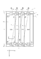
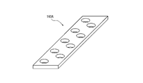
- FIG. 1 is an external view of the thermoelectric conversion module 1 according to the first embodiment of the present invention.
- FIG. 2 is a cross-sectional view of the thermoelectric conversion module 1 along the line L1-L1 shown in FIG.
- FIG. 3 is a diagram showing the wiring layer 30 shown in FIG. The configuration shown in FIG. 3 corresponds to the configuration after performing the wiring layer 30 forming step S11 as shown in FIG. 6 to be described later.
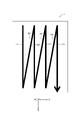
- FIG. 4 is a diagram showing a current path in the thermoelectric conversion module shown in FIG.
- thermoelectric conversion module 1 can be arranged in the heat source 2.
- the thermoelectric conversion module 1 includes a first edge portion 1H and a second edge portion 1L in a sheet substrate 10 described later.
- the first edge portion 1H and the second edge portion 1L face each other.
- the first edge portion 1H may be located near the heat source 2 when the thermoelectric conversion module 1 is arranged in the heat source 2.
- the second edge portion 1L may be located away from the heat source 2 when the thermoelectric conversion module 1 is arranged in the heat source 2.
- the temperature near the first edge portion 1H can be higher than the temperature near the second edge portion 1L because the first edge portion 1H is located closer to the heat source 2 than the second edge portion 1L. In other words, the temperature near the second edge portion 1L can be lower than the temperature near the first edge portion 1H.
- the first direction A1 is the direction in which the first edge portion 1H and the second edge portion 1L face each other. In the present embodiment, it is assumed that the first direction A1 is the direction from the second edge portion 1L of the thermoelectric conversion module 1 toward the first edge portion 1H.
- the second direction A2 is a direction orthogonal to the first direction A1.
- the second direction A2 does not have to be orthogonal to the first direction A1 as long as it intersects the first direction A1.
- the second direction A2 is the direction from the left side of the paper surface of FIG. 1 toward the right side of the paper surface.
- the third direction A3 is a direction orthogonal to the plane including the first direction A1 and the second direction A2.
- the third direction A3 is the direction from the back side of the paper surface of FIG. 1 toward the front side of the paper surface.
- upper shall refer to the A3 side in the third direction unless otherwise specified.
- downward shall mean the opposite direction side of the third direction A3 unless otherwise specified.
- the shape of the thermoelectric conversion module 1 seen from the third direction A3 is a rectangular shape such as a rectangular shape.
- the thermoelectric conversion module 1 includes a sheet substrate 10, thermoelectric conversion elements 21, 22, 23, 24, first joining members 71, 72, 73, 74, and second joining members 81, 82. , 83, 84 and so on.
- the thermoelectric conversion module 1 includes a wiring layer 30.
- the wiring layer 30 is located in the sheet substrate 10.
- the wiring layer 30 may be located on the back surface 12B side of the insulating layer 12 described later.
- the wiring layer 30 has first electrodes 41, 42, 43, 44, second electrodes 51, 52, 53, 54, and wiring 61, 62, 63.
- thermoelectric conversion element 20 shows a thermoelectric conversion module 1 including four thermoelectric conversion elements 20.
- the number of the plurality of thermoelectric conversion elements 20 included in the thermoelectric conversion module 1 may be any number.
- FIG. 3 shows a wiring layer 30 having four first electrodes 40, four second electrodes 50, and three wirings 60.
- the number of the first electrodes 40, the number of the second electrodes 50, and the number of the wirings 60 of the wiring layer 30 may correspond to the number of the thermoelectric conversion elements 20 included in the thermoelectric conversion module 1.
- FIG. 1 shows a thermoelectric conversion module 1 including four first joining members 70 and four second joining members 80.
- the number of the first joining member 70 and the number of the second joining members 80 included in the thermoelectric conversion module 1 may correspond to the number of the thermoelectric conversion elements 20 included in the thermoelectric conversion module 1.
- the numbers An of each of the thermoelectric conversion elements 21, 22, 23, and 24 are No. 1, No. 2, No. 3, and No. 4.
- the numbers B n assigned to the first electrodes 41, 42, 43, 44 along the second direction A2 are No. 1, No. 2, No. 3, and No. 4.
- the numbers Cn assigned to the second electrodes 51, 52, 53, 54 along the second direction A2 are No. 1, No. 2, No. 3, and No. 4.
- the numbers Dn assigned to the wirings 61, 62, and 63 along the second direction A2 are No. 1, No. 2, and No. 3.
- the numbers En of each of the first joining members 71, 72, 73, 74 are No. 1, No. 2, No. 3, and No. 4.
- the numbers F n of each of the second joining members 81, 82, 83, 84 are No. 1, No. 2, No. 3, and No. 4.
- the sheet substrate 10 as shown in FIG. 1 has an insulating property.
- the sheet substrate 10 may have flexibility.
- the material for forming the sheet substrate 10 is not particularly limited, and any insulating material can be used.
- the shape of the sheet substrate 10 seen from the third direction A3 is a quadrangle such as a rectangle.
- the sheet substrate 10 may be parallel to the surface including the first direction A1 and the second direction A2.
- the sheet substrate 10 includes the above-mentioned first edge portion 1H and the above-mentioned second edge portion 1L. As shown in FIG. 2, the sheet substrate 10 includes a front surface 10A and a back surface 10B. The front surface 10A and the back surface 10B face each other. The surface 10A is a surface of the sheet substrate 10 facing the third direction A3. The back surface 10B is a surface of the sheet substrate 10 facing the opposite direction of the third direction A3.
- the sheet substrate 10 has a substrate 11 and an insulating layer 12.
- the substrate 11 has an insulating property.
- the substrate 11 may have flexibility.
- the material for forming the substrate 11 is not particularly limited, and any material such as polyimide or epoxy glass can be used.
- the shape of the substrate 11 seen from the third direction A3 is a rectangular shape such as a rectangular shape.
- the substrate 11 may be parallel to the plane including the first direction A1 and the second direction A2.
- the substrate 11 includes a front surface 11A and a back surface 11B.
- the front surface 11A and the back surface 11B face each other.
- the surface 11A is a surface of the substrate 11 facing the third direction A3.
- the back surface 11B is a surface of the substrate 11 facing the opposite direction of the third direction A3.
- the back surface 11B may correspond to the back surface 10B of the sheet substrate 10.
- the insulating layer 12 has an insulating property.
- the insulating layer 12 may have flexibility.
- the material for forming the insulating layer 12 is not particularly limited, and any insulating material can be used.
- the insulating layer 12 may be located on the surface 11A of the substrate 11. As shown in FIG. 1, the shape of the insulating layer 12 seen from the third direction A3 is a rectangular shape such as a rectangular shape.
- the insulating layer 12 may be parallel to the surface including the first direction A1 and the second direction A2.
- the insulating layer 12 includes a front surface 12A and a back surface 12B.
- the front surface 12A and the back surface 12B face each other.
- the surface 12A is a surface of the insulating layer 12 facing the third direction A3.
- the surface 12A may correspond to the surface 10A of the sheet substrate 10.
- the back surface 12B is a surface of the insulating layer 12 facing the opposite direction of the third direction A3.
- thermoelectric conversion elements 21 to 24 are p-type thermoelectric conversion elements or n-type thermoelectric conversion elements.
- thermoelectric conversion material forming the thermoelectric conversion element 20 one of the p-type thermoelectric conversion element and the n-type thermoelectric conversion element may have higher durability than the other. Since all of the plurality of thermoelectric conversion elements 20 included in the thermoelectric conversion module 1 are p-type thermoelectric conversion elements or n-type thermoelectric conversion elements, the thermoelectric conversion module 1 can be excellent in durability.
- thermoelectric conversion material for forming the thermoelectric conversion element 20 is not particularly limited, and is not particularly limited, and is bismuth tellurium-based compound, antimony-based compound, silicon-based compound, metal oxide-based compound, Whistler alloy-based compound, and conductive polymer.
- Compounds, conductive fibers, composite materials thereof and the like can be used.
- conductive fibers it is preferable to use conductive fibers, and it is more preferable to use fibrous carbon nanostructures such as carbon nanotubes (hereinafter, also referred to as “CNT”). This is because if CNTs are used, the mechanical strength of the thermoelectric conversion module 1 of the present invention can be further improved and the weight can be reduced.
- CNT carbon nanotubes
- the CNT is not particularly limited, and a single-walled CNT and / or a multi-walled CNT can be used, but the CNT is preferably a single-walled CNT. This is because single-walled CNTs tend to have superior thermoelectric characteristics (Seebeck coefficient).
- the single-walled carbon nanotubes are used when CNTs are synthesized by a chemical vapor deposition method (CVD method) by supplying a raw material compound and a carrier gas onto a substrate having a catalyst layer for CNT production on the surface.
- CVD method chemical vapor deposition method
- SGCNT oxidizing agent
- CNT manufactured according to such a method may be referred to as "SGCNT”
- SGCNT has a feature that there are many bends.
- CNTs are considered to have high thermal conductivity due to electron transfer, but also have a high effect of lowering thermal conductivity due to phonon vibration.
- SGCNT has more bends than CNTs manufactured according to other general methods, it has a structure in which phonon vibration is less likely to be amplified, and it is possible to suppress a decrease in thermal conductivity due to phonon vibration. .. Therefore, SGCNT can be a more superior material as a thermoelectric conversion material as compared with other general CNTs.
- thermoelectric conversion elements 21 to 24 may be formed including CNTs. With such a configuration, the mechanical strength of the thermoelectric conversion module 1 can be further improved, and the weight of the thermoelectric conversion module 1 can be reduced.
- thermoelectric conversion elements 21 to 24 may be p-type thermoelectric conversion elements, for example, when the thermoelectric conversion material for forming the thermoelectric conversion element 20 is an organic material such as CNT.
- the thermoelectric conversion material is an organic material
- oxidation of the thermoelectric conversion element 20 by oxygen, moisture, or the like in the atmosphere may be the main cause of deterioration of the characteristics of the thermoelectric conversion element 20.
- the p-type thermoelectric conversion element is more susceptible to oxidation due to oxygen and moisture in the atmosphere than the p-type thermoelectric conversion element, so that the p-type thermoelectric conversion element is more susceptible than the n-type thermoelectric conversion element. It can be more durable.
- the thermoelectric conversion module 1 can be excellent in durability because all of the plurality of thermoelectric conversion elements 20 included in the thermoelectric conversion module 1 are p-type thermoelectric conversion elements. ..
- thermoelectric conversion element 20 extends along the first direction A1.
- the shape of the thermoelectric conversion element 20 seen from the third direction A3 is a long shape such as a rectangular shape.
- the longitudinal direction of the thermoelectric conversion element 20 is along the first direction A1.
- the longitudinal direction of the thermoelectric conversion element 20 may be parallel to the first direction A1.
- the thermoelectric conversion elements 21 to 24 may have the same shape.
- the cross-sectional shape of the thermoelectric conversion element 20 may be a thin film.
- thermoelectric conversion elements 21 to 24 are arranged so as to be arranged along the second direction A2 on the surface 10A of the sheet substrate 10, for example, the surface 12A of the insulating layer 12.
- the thermoelectric conversion elements 21 to 24 are arranged so as to be arranged along the second direction A2 on the surface 12A side of the insulating layer 12.
- the thermoelectric conversion elements 21 to 24 may be arranged along the second direction A2 with a gap. The width of the gap may be arbitrary as long as insulation between two thermoelectric conversion elements 20 adjacent to each other in the second direction A2 can be secured.
- each of the thermoelectric conversion elements 21 to 24 may be a rectangular shape having substantially the same dimensions. Since the shapes of all the thermoelectric conversion elements 21 to 24 are rectangular with substantially the same dimensions, the thermoelectric conversion elements 21 to 24 can be efficiently arranged on the surface 10A of the sheet substrate 10. With such a configuration, the thermoelectric conversion module can be miniaturized.
- the thermoelectric conversion element 20 includes a first end portion 20H and a second end portion 20L in the first direction A1.
- the first end portion 20H is located toward the first edge portion 1H of the thermoelectric conversion module 1.
- the second end portion 20L is located toward the second edge portion 1L of the thermoelectric conversion module 1.
- the first end portions 20H of the thermoelectric conversion elements 21, 22, 23, 24 are “first end portion 21H”, “first end portion 22H”, “first end portion 23H”, and “first end”, respectively. It is also described as “Part 24H”.
- the second end 20L of the thermoelectric conversion elements 21, 22, 23, 24 are “second end 21L", “second end 22L", “second end 23L", and “second end”, respectively. It is also described as "Part 24L". In the configuration shown in FIG.
- the positions of the first end portions 21H to 24H in the first direction A1 are different. However, the positions of the first end portions 21H to 24H in the first direction A1 may be the same. Further, in the configuration shown in FIG. 1, the positions of the second end portions 21L to 24L in the first direction A1 are different. However, the positions of the second end portions 21L to 24L in the first direction A1 may be the same.
- the thermoelectric conversion element 20 can generate electricity by utilizing the temperature difference between the first end portion 20H and the second end portion 20L. Specifically, the temperature of the first end portion 20H of the thermoelectric conversion element 20 is such that the first end portion 20H is located closer to the first edge portion 1H than the second end portion 20L, so that the second end portion 20L Can be higher than the temperature of. When the temperature of the first end portion 20H becomes higher than the temperature of the second end portion 20L, a temperature difference may occur between the first end portion 20H and the second end portion 20L. Due to the temperature difference between the first end portion 20H and the second end portion 20L, a temperature gradient may occur in the thermoelectric conversion element 20. The thermoelectric conversion element 20 can generate electric power by generating an electromotive force due to the Zeebeck effect caused by this temperature gradient.
- thermoelectric conversion element 20 When the thermoelectric conversion element 20 generates electricity, a current flowing through the thermoelectric conversion element 20 may be generated. For example, as shown in FIG. 4, each of the currents I21, I22, I23, and I24 flowing in each of the thermoelectric conversion elements 21, 22, 23, 24 toward the first direction A1 can be generated.
- thermoelectric conversion elements 21 to 24 have a length along the first direction A1 of each of the thermoelectric conversion elements 21 to 24 so that the electric resistance values of the thermoelectric conversion elements 21 to 24 are substantially the same. It may be configured by adjusting the width along the second direction A2 of each of 24 to 24 and the thickness of the thermoelectric conversion elements 21 to 24 in the third direction A3 of each of the thermoelectric conversion elements 21 to 24.
- the thermoelectric conversion element 20 having a small electric resistance value may cause the thermoelectric conversion module 1. The current is fixed.
- thermoelectric conversion elements 21 to 24 Since the electric resistance values of the thermoelectric conversion elements 21 to 24 are substantially the same, it can be suppressed that the current that can be generated in the thermoelectric conversion module 1 is determined by the thermoelectric conversion element 20 having a small electric resistance value. With such a configuration, the power loss in the thermoelectric conversion module 1 can be reduced.
- the first electrode 40, the second electrode 50, and the wiring 60 may be formed of the same conductive material or may be formed of different conductive materials.
- the conductive material for forming each of the first electrode 40, the second electrode 50, and the wiring 60 is not particularly limited, and any metal such as copper or aluminum can be used.
- any metal such as copper or aluminum can be used.
- it is assumed that the first electrode 40, the second electrode 50, and the wiring 60 are made of the same conductive material.
- the first electrode 40 may be located on the surface 11A of the substrate 11.
- the first electrodes 41 to 44 may be arranged along the second direction A2 with a gap.
- the width of the gap may be arbitrary as long as the insulation between the two first electrodes 40 adjacent to each other in the second direction A2 can be secured.
- At least a part of the first electrode 40 may be exposed from the sheet substrate 10, for example, the insulating layer 12. At least a part of the first electrode 40 exposed from the sheet substrate 10, for example, the insulating layer 12, may be electrically connected to the first end portion 20H of the thermoelectric conversion element 20 by the first joining member 70.
- At least a part of the first electrode 40 of the number B n exposed from the insulating layer 12 is of the same number An as the number B n by the first joining member 70 of the same number En as the number B n . It may be electrically connected to the first end portion 20H of the thermoelectric conversion element 20.
- at least a part of the first electrode 41 exposed from the insulating layer 12 is electrically connected to the first end portion 21H of the first thermoelectric conversion element 21 by the first first joining member 71.
- at least a part of the second first electrode 42 exposed from the insulating layer 12 is electrically connected to the first end portion 22H of the second thermoelectric conversion element 22 by the second first joining member 72.
- At least a part of the No. 3 first electrode 43 exposed from the insulating layer 12 is electrically connected to the first end portion 23H of the No. 3 thermoelectric conversion element 23 by the No. 3 first joining member 73.
- at least a part of the No. 4 first electrode 44 exposed from the insulating layer 12 is electrically connected to the first end portion 24H of the No. 4 thermoelectric conversion element 24 by the No. 4 first joining member 74.
- the position of the first electrode 40 of the number B n in the second direction A2 may be the same as the position of the thermoelectric conversion element 20 of the same number An as the number B n in the second direction A2.
- the first electrode 40 of the number B n may be located closer to the first edge portion 1H of the thermoelectric conversion module 1 than the first end portion 20H of the thermoelectric conversion element 20 having the same number An as the number B n .
- the first electrode 40 of the number B n may be located between the first end portion 20H of the thermoelectric conversion element 20 having the same number An as the number B n and the first edge portion 1H of the thermoelectric conversion module 1.
- the first electrode 41 is located between the first end portion 21H and the first edge portion 1H of the first thermoelectric conversion element 21.
- the second first electrode 42 is located between the first end portion 22H and the first edge portion 1H of the second thermoelectric conversion element 22.
- the No. 3 first electrode 43 is located between the first end portion 23H and the first edge portion 1H of the No. 3 thermoelectric conversion element 23.
- the No. 4 first electrode 44 is located between the first end portion 24H and the first edge portion 1H of the No. 4 thermoelectric conversion element 24.
- the electric resistance value of the first electrode 40 may be equal to or higher than the electric resistance value of the wiring 60.
- the first electrode 40 may be configured so that the electric resistance value of the first electrode 40 is equal to or higher than the electric resistance value of the wiring 60.
- the width of the first electrode 40 along the second direction A2 is described later in the wiring 60. It may be wider than the width W60 as shown in FIG. With such a configuration, the electric resistance value of the first electrode 40 can be equal to or higher than the electric resistance value of the wiring 60.
- a take-out wiring for taking out the electric power generated by the thermoelectric conversion module 1 may be electrically connected to any of the plurality of first electrodes 40.
- the take-out wiring may be electrically connected to the first electrode 44.
- the second electrode 50 may be located on the surface 11A of the substrate 11.
- the second electrodes 51 to 54 may be arranged along the second direction A2 with a gap.
- the width of the gap may be arbitrary as long as the insulation between the two second electrodes 50 adjacent to each other in the second direction A2 can be secured.
- At least a part of the second electrode 50 may be exposed from the sheet substrate 10, for example, from the insulating layer 12. At least a part of the second electrode 50 exposed from the sheet substrate 10 for example, the insulating layer 12, may be electrically connected to the second end portion 20L of the thermoelectric conversion element 20 by the first joining member 70.
- At least a part of the second electrode 50 of the number Cn exposed from the insulating layer 12 is thermoelectrically charged with the same number An as the number Cn by the second bonding member 80 of the same number Fn as the number Cn. It may be electrically connected to the second end portion 20L of the conversion element 20.
- at least a part of the first second electrode 51 exposed from the insulating layer 12 is electrically connected to the second end portion 21L of the first thermoelectric conversion element 21 by the first second joining member 81. ..
- at least a part of the second electrode 52 exposed from the insulating layer 12 is electrically connected to the second end portion 22L of the second thermoelectric conversion element 22 by the second joining member 82. ..
- At least a part of the second electrode 53 of No. 3 exposed from the insulating layer 12 is electrically connected to the second end portion 23L of the thermoelectric conversion element 23 of No. 3 by the second joining member 83 of No. 3. ..
- at least a part of the No. 4 second electrode 54 exposed from the insulating layer 12 is electrically connected to the second end portion 24L of the No. 4 thermoelectric conversion element 24 by the No. 4 second joining member 84. ..
- the position of the second electrode 50 of the number C n in the second direction A2 may be the same as the position of the thermoelectric conversion element 20 of the same number An as the number Cn in the second direction A2.
- the second electrode 50 of the number C n may be located closer to the second edge portion 1L of the thermoelectric conversion module 1 than the second end portion 20L of the thermoelectric conversion element 20 having the same number An as the number C n .
- the second electrode 50 of the number Cn may be located between the second end portion 20L of the thermoelectric conversion element 20 having the same number An as the number Cn and the second edge portion 1L of the thermoelectric conversion module 1.
- the first second electrode 51 is located between the second end portion 21L and the second edge portion 1L of the first thermoelectric conversion element 21.
- the second electrode 52 of No. 2 is located between the second end portion 22L of the thermoelectric conversion element 22 of No. 2 and the second edge portion 1L. Further, the second electrode 53 of No. 3 is located between the second end portion 23L and the second edge portion 1L of the thermoelectric conversion element 23 of No. 3. Further, the No. 4 second electrode 54 is located between the second end portion 24L and the second edge portion 1L of the No. 4 thermoelectric conversion element 24.
- the electric resistance value of the second electrode 50 may be equal to or higher than the electric resistance value of the wiring 60.
- the second electrode 50 may be configured so that the electric resistance value of the second electrode 50 is equal to or higher than the electric resistance value of the wiring 60.
- the width of the second electrode 50 along the second direction A2 is shown in FIG. It may be wider than the width W60 as shown. With such a configuration, the electric resistance value of the second electrode 50 can be equal to or higher than the electric resistance value of the wiring 60.
- a take-out wiring for taking out the electric power generated by the thermoelectric conversion module 1 may be electrically connected to any of the plurality of second electrodes 50.
- the take-out wiring may be electrically connected to the second electrode 51.
- the wiring 60 may be located in the sheet substrate 10. As shown in FIG. 3, the wiring 60 may be located on the surface 11A of the substrate 11 together with the first electrode 40 and the second electrode 50. The wiring 60 may be located on the back surface 12B side of the insulating layer 12. The wiring 60 may be located on the back surface 12B side of the insulating layer 12 together with the first electrode 40 and the second electrode 50.
- the wiring 60 electrically connects the thermoelectric conversion elements 20 adjacent to each other in the second direction A2 at both ends of the thermoelectric conversion element 20, that is, the first end portion 20H and the second end portion 20L.
- the wiring 60 is a first electrode 40 electrically connected to the first end portion 20H of one thermoelectric conversion element 20 in two thermoelectric conversion elements 20 adjacent to each other in the second direction A2, and the other.
- the second electrode 50 which is electrically connected to the second end portion 20L of the thermoelectric conversion element 20 of the above, is electrically connected.
- the plurality of wirings 60 are arranged in the order of the numbers Ann assigned to the thermoelectric conversion element 20 by electrically connecting the plurality of first electrodes 40 and the plurality of second electrodes 50.
- a plurality of thermoelectric conversion elements 20 may be electrically connected in series.
- the first electrode 40 of the same number En as the number D n and the second electrode 50 of the number F n + 1 larger than the number D n are electrically connected. good.
- One end of the wiring 60 of the number D n may be connected to the first electrode 40 of the same number En as the number D n .
- the other end of the wiring 60 of the number D n may be electrically connected to the second electrode 50 of the number F n + 1 , which is one larger than the number D n .
- the wiring 60 of the number D n may extend linearly from the first electrode 40 of the same number En as the number D n to the second electrode 50 of the number F n + 1 which is one larger than the number D n .
- one end of the first wiring 61 is electrically connected to the first electrode 41.
- the other end of the first wiring 61 is electrically connected to the second second electrode 52 having a number one larger than that of the first wiring 61.
- One end of the second wiring 62 is electrically connected to the second first electrode 42.
- the other end of the second wire 62 is electrically connected to the third second electrode 53, which has a larger number than the second wire 62.
- One end of the No. 3 wiring 63 is electrically connected to the No. 3 first electrode 43.
- the other end of the No. 3 wiring 63 is electrically connected to the No. 4 second electrode 54, which has a larger number than the No. 3.
- thermoelectric conversion elements 20 are electrically connected in series in the order of the numbers Ann assigned to the thermoelectric conversion elements 20.
- thermoelectric conversion elements 220 are electrically connected in series, one current path may be generated in the thermoelectric conversion module 1 as shown in FIG. 4 when the plurality of thermoelectric conversion elements 20 generate electric power.
- the currents I61, I62, I63, I64 are the currents flowing through the wirings 61, 62, 63, 64.
- the first joining member 70 has conductivity.
- the first joining member 70 may be formed of any member such as silver paste or solder.
- the first joining member 70 of the number En electrically connects the first end portion 20H of the thermoelectric conversion element 20 of the same number An as the number En and the first electrode 40 of the same number An as the number En. You may connect.
- the first joining member 70 of the number En is in the first direction A1 from the first end 20H of the thermoelectric conversion element 20 of the same number An as the number En to the first electrode 40 of the same number An as the number En. It may extend along.
- the first joining member 71 electrically connects the first end portion 21H of the thermoelectric conversion element 21 of No. 1 and the first electrode 41 of No. 1.
- the first first joining member 71 extends from the first end 21H of the first thermoelectric conversion element 21 to the first first electrode 41 along the first direction A1.
- the second first joining member 72 electrically connects the first end portion 22H of the second thermoelectric conversion element 22 and the second first electrode 42.
- the second first joining member 72 extends from the first end 22H of the second thermoelectric conversion element 22 to the second first electrode 42 along the first direction A1.
- the No. 3 first joining member 73 electrically connects the first end portion 23H of the No. 3 thermoelectric conversion element 23 and the No. 3 first electrode 43.
- the No. 4 first joining member 74 electrically connects the first end portion 24H of the No. 4 thermoelectric conversion element 24 and the No. 4 first electrode 44.
- the No. 4 first joining member 74 extends from the first end portion 24H of the No. 4 thermoelectric conversion element 24 to the No. 4 first electrode 44 along the first direction A1.
- the electric resistance value of the first joining member 70 may be equal to or higher than the electric resistance value of the wiring 60.
- the first joining member 70 may be configured so that the electric resistance value of the first joining member 70 is equal to or higher than the electric resistance value of the wiring 60.
- the electric resistance value of the first joining member 70 may be equal to or higher than the electric resistance value of the wiring 60.
- the material of the first joining member 70 may be silver paste.
- the second joining member 80 has conductivity.
- the second joining member 80 may be formed of any member such as silver paste or solder.
- the second joining member 80 having the number F n electrically connects the second end 20L of the thermoelectric conversion element 20 having the same number An as the number F n and the second electrode 50 having the same number C n as the number F n . You may connect.
- the second joining member 80 of the number F n is in the first direction A1 from the second end 20L of the thermoelectric conversion element 20 of the same number An as the number F n to the second electrode 50 of the same number C n as the number F n . It may extend along.
- the first second joining member 81 electrically connects the second end portion 21L of the first thermoelectric conversion element 21 and the first second electrode 51.
- the first second joining member 81 extends from the second end 21L of the first thermoelectric conversion element 21 to the first second electrode 51 along the first direction A1.
- the second joining member 82 electrically connects the second end portion 22L of the second thermoelectric conversion element 22 and the second second electrode 52.
- the second joining member 82 of No. 2 extends from the second end 22L of the thermoelectric conversion element 22 of No. 2 to the second electrode 52 of No. 2 along the first direction A1.
- the second joining member 83 of No. 3 electrically connects the second end portion 23L of the thermoelectric conversion element 23 of No. 3 and the second electrode 53 of No. 3.
- the second joining member 83 of No. 3 extends from the second end 23L of the thermoelectric conversion element 23 of No. 3 to the second electrode 53 of No. 3 along the first direction A1. Further, the second joining member 84 of No. 4 electrically connects the second end portion 24L of the thermoelectric conversion element 24 of No. 4 and the second electrode 54 of No. 4. The second joining member 84 of No. 4 extends from the second end portion 24L of the thermoelectric conversion element 24 of No. 4 to the second electrode 54 of No. 4 along the first direction A1.
- the electric resistance value of the second joining member 80 may be equal to or higher than the electric resistance value of the wiring 60.
- the second joining member 80 may be configured so that the electric resistance value of the second joining member 80 is equal to or higher than the electric resistance value of the wiring 60.
- the electric resistance value of the second joining member 80 may be equal to or higher than the electric resistance value of the wiring 60.
- the material of the second joining member 80 may be silver paste.
- the thermal resistance value of the wiring 60 is equal to or higher than the thermal resistance value of the thermoelectric conversion element 20.
- the wiring 60 may be configured so that the thermal resistance value of the wiring 60 is equal to or higher than the thermal resistance value of the thermoelectric conversion element 20.
- thermoelectric conversion element 21 it can be suppressed that the heat of the first end portion 21H of the thermoelectric conversion element 21 is transferred to the second end portion 22L of the thermoelectric conversion element 22 via the wiring 61.
- the first end 20H and the second end 20H of the thermoelectric conversion element 20 are suppressed.
- the temperature difference between the end portion 20L and the end portion 20L becomes small.
- FIG. 5 is a diagram illustrating the setting of the thermal resistance value of the thermoelectric conversion element 20 and the wiring 60.
- the length, width, and thickness of the thermoelectric conversion element 20 are also described as “length L 20 ", “width W 20 “, and “thickness T 20 “, respectively.
- the length L 20 is the length of the thermoelectric conversion element 20 as shown in FIG. 1 along the first direction A1.
- the width W 20 is the width of the thermoelectric conversion element 20 as shown in FIG. 1 along the second direction A2.
- the thickness T 20 is the thickness of the thermoelectric conversion element 20 in the third direction A3 as shown in FIG.
- the length, width and thickness of the wiring 60 are also described as “length L 60 ", “width W 60 “ and “thickness T 60 “, respectively.
- the length L 60 is from the first electrode 40 of the number B n where the wiring 60 of the number D n is the same as the number D n to the second electrode 50 of the number C n + 1 which is one larger than the number D n as shown in FIG. It is the length to extend.
- the thickness T 60 is the thickness of the wiring 60 in the third direction A3 as shown in FIG.
- the width W 60 extends from the first electrode 40 of the number B n , which is the same as the number D n , to the second electrode 50 of the number C n + 1 , which is one larger than the number D n , as shown in FIG. It is the width of the wiring 60 in the direction orthogonal to the direction and the third direction A3.
- the length L 60 , the width W 60 , and the thickness T 60 of the wiring 60 may be set so that the thermal resistance value of the wiring 60 is equal to or higher than the thermal resistance value of the thermoelectric conversion element 20.
- the length L 60 , the width W 60 , and the thickness T 60 of the wiring 60 may be set so as to satisfy the following equation (1). (1 / ⁇ 20 ) ⁇ ⁇ L 20 / (T 20 ⁇ W 20 ) ⁇ ⁇ (1 / ⁇ 60 ) ⁇ ⁇ L 60 / (T 60 ⁇ W 60 ) ⁇ Equation (1)
- the thermal conductivity ⁇ 20 is the thermal conductivity of the thermoelectric conversion element 20.
- the thermal conductivity ⁇ 60 is the thermal conductivity of the thermoelectric conversion element 20.
- the thermal resistance value of the wiring 60 may be equal to or higher than the thermal resistance value of the thermoelectric conversion element 20, and the electric resistance value of the wiring 60 may be equal to or lower than the electrical resistance value of the thermoelectric conversion element 20. That is, the wiring 60 is configured so that the thermal resistance value of the wiring 60 is equal to or higher than the thermal resistance value of the thermoelectric conversion element 20 and the electric resistance value of the wiring 60 is equal to or lower than the electrical resistance value of the thermoelectric conversion element 20. It's okay.
- the length L 60 , the width W 60 , and the thickness T 60 of the wiring 60 may be set so as to satisfy the following equation (2) while satisfying the equation (1).
- the electric resistance value of the wiring 60 becomes equal to or less than the electric resistance value of the thermoelectric conversion element 20, it is suppressed that the current flowing through the thermoelectric conversion module 1 as shown in FIG. 4 is limited by the electric resistance value of the wiring 60. obtain.
- the electric conductivity ⁇ 20 is the electric conductivity of the thermoelectric conversion element 20.
- the electric conductivity ⁇ 60 is the electric conductivity of the thermoelectric conversion element 20.
- the total electric resistance value of the wirings 61 to 63 may be set to be about 10% of the total electric resistance value of the thermoelectric conversion module 1.
- the total electric resistance values of the wirings 61 to 63 are the sum of the electric resistance values of the thermoelectric conversion module 1. It can be about the design error of the overall electrical resistance value.
- thermoelectric conversion element 20 is 15 [W / mK]
- electric conductivity ⁇ 20 of the thermoelectric conversion element 20 is 900 [S / cm].
- the length L 20 , the width W 20 and the height H 20 of the thermoelectric conversion element 20 are 15 [mm], 1.5 [mm] and 50 [ ⁇ m], respectively.
- the thermal resistance value of the thermoelectric conversion element 20 having such a configuration is 13.3 [K / W].
- the electric resistance value of the thermoelectric conversion element 20 is 2.222 [ ⁇ ].
- the material of the wiring 60 is copper.
- the thermal conductivity ⁇ 60 of the wiring 60 is 400 [W / mK]
- the electric conductivity ⁇ 60 of the wiring 60 is 6 ⁇ 10 7 [S / cm].
- the length L 60 , the width W 60 , and the thickness T 60 of the wiring 60 are set to 16 [mm], 0.15 [mm], and 15 [ ⁇ m], respectively.
- the thermal resistance value of the wiring 60 having such a configuration is 17.8 [K / W].
- the thermal resistance value of the wiring 60 is 17.8 [K / W], which is larger than the thermal resistance value of the thermoelectric conversion element 20 of 13.3 [K / W].
- the electric resistance value of the wiring 60 is 0.001 [ ⁇ ].
- the electric resistance value of 0.001 [ ⁇ ] of the wiring 60 is larger than the electric resistance value of 2.222 [ ⁇ ] of the thermoelectric conversion element 20.
- Example 2 as in Example 1, the material of the wiring 60 is copper.
- the length L 60 , the width W 60 , and the thickness T 60 of the wiring 60 are set to 16 [mm], 0.15 [mm], and 20 [ ⁇ m], respectively.
- the thermal resistance value of the wiring 60 having such a configuration is 20 [K / W].
- the thermal resistance value of 20 [K / W] of the wiring 60 is larger than the thermal resistance value of 13.3 [K / W] of the thermoelectric conversion element 20.
- the electric resistance value of the wiring 60 is 0.001 [ ⁇ ].
- the electric resistance value of 0.001 [ ⁇ ] of the wiring 60 is larger than the electric resistance value of 2.222 [ ⁇ ] of the thermoelectric conversion element 20.
- thermoelectric conversion module 1 the thermal resistance value of the wiring 60 is equal to or higher than the thermal resistance value of the thermoelectric conversion element 20. With such a configuration, as described above, it is possible to suppress the temperature difference between the first end portion 20H and the second end portion 20L in the thermoelectric conversion element 20 from becoming small. By suppressing the decrease in temperature difference between the first end portion 20H and the second end portion 20L, it is possible to suppress a decrease in the generated power of the thermoelectric conversion element 20. Therefore, according to the present embodiment, the thermoelectric conversion module 1 in which the decrease in the generated power is suppressed can be provided.
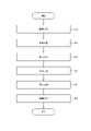
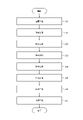
- FIG. 6 is a flowchart showing the flow of the manufacturing method of the thermoelectric conversion module 1 shown in FIG.
- the method for manufacturing the thermoelectric conversion module 1 according to the present embodiment includes an arrangement step S10, a forming step S11, S12, S13, S14, and a connecting step S15, which will be described later.
- the manufacturing method of the thermoelectric conversion module 1 according to the present embodiment is not limited to the manufacturing method described below.
- the arrangement step S10 is a step of arranging the metal foil 130 on the substrate 11 as shown in FIG.
- the metal leaf 130 may be arranged on the surface 11A of the substrate 11.
- the metal leaf 130 may be adhered to the surface 11A of the substrate 11 by any adhesive having thermal conductivity.
- the metal foil 130 can become the wiring layer 30 through the formation step S11 and the like described later.
- the metal leaf 130 may be any metal leaf such as copper or aluminum.
- the forming step S11 is a step of forming the wiring layer 30 on the surface 11A of the substrate 11 as shown in FIG. 3 by patterning the metal foil 130.
- Known photolithography or the like may be used for patterning the metal foil 130.
- the forming step S12 is a step of forming the insulating layer 12 on the substrate 11 and the wiring layer 30 as shown in FIG.
- the insulating layer 12 may be formed by applying an insulating material on the substrate 11 and the wiring layer 30 as shown in FIG.
- the insulating layer 12 is formed on the substrate 11 and the wiring layer 30 so that the first electrode 40 and the second electrode 50 are exposed.
- the first electrode 40 and the second electrode 50 can be said to be both ends of the wiring 60.
- the forming step S12 can be said to be a step of forming the insulating layer 12 on the substrate 11 and the wiring layer 30 so that only both ends of the wiring 60 are exposed from the insulating layer 12.
- the sheet substrate 10 is formed by forming the insulating layer 12 on the surface 11A of the substrate 11. That is, the sheet substrate 10 has a substrate 11 and an insulating layer 12 formed on the surface 11A of the substrate 11.
- the forming step S13 is a step of forming a thermoelectric conversion element layer on the insulating layer 12.
- the thermoelectric conversion element layer is a layer formed including CNT.
- the thermoelectric conversion element layer can become the thermoelectric conversion element 20 after undergoing the formation step S16 or the like described later.
- the mechanical strength of the thermoelectric conversion module 1 can be further improved and the weight can be reduced. Since the thermoelectric conversion element layer is formed to include CNTs, the thermoelectric conversion module 1 can be manufactured with further improved mechanical strength and lighter weight.
- the thermoelectric conversion element layer is a CNT sheet 120 (carbon nanotube sheet) as shown in FIG.
- the CNT sheet 120 is formed to include CNTs.
- the forming step S13 is a step of arranging the CNT sheet 120 on the insulating layer 12.
- the CNT sheet 120 may be arranged, for example, on the surface 12A of the insulating layer 12, that is, the surface 10A of the sheet substrate 10.
- the CNT sheet 120 may be adhered to the surface 12A of the insulating layer 12 by any adhesive sheet such as an epoxy resin.
- the CNT sheet 120 can become the thermoelectric conversion element 20 after undergoing the formation step S14 or the like described later.
- a p-type thermoelectric conversion element a p-type CNT sheet 120 may be used.
- an n-type CNT sheet 120 may be used.
- the thickness of the CNT sheet 120 in the third direction A3 may be about 50 [ ⁇ m].
- the electrical characteristics of the thermoelectric conversion element 20 can be exhibited. For example, as an electrical characteristic of the thermoelectric conversion element 20, the amount of power generation of the thermoelectric conversion element 20 can be secured to some extent.
- a CNT coating film formed by a coating method using a CNT dispersion liquid may be arranged on the insulating layer 12.
- the CNT coating film there are problems that the conductivity of the CNT coating film is lowered and the independence of the CNT coating film is lowered due to the aggregation of CNTs in the process of drying the CNT dispersion liquid. Can occur. Further, in order to form a CNT coating film having a thickness of 50 [ ⁇ m] by the coating method, it is required to add a binder to the CNT dispersion liquid.
- the CNT sheet 120 is not particularly limited, and the CNT sheet 120 described in Japanese Patent Application No. 2018-065290 can be used.
- the CNT sheet 120 may include a bundle in which a plurality of single-walled CNTs are intertwined.
- the thickness of the bundle may be 1 [ ⁇ m] or less.
- the fluffing of the cut surface of the thermoelectric conversion element 20 by the laser in the forming step S14 described later can be reduced. By reducing the fluffing of the thermoelectric conversion element 20, it is possible to suppress the occurrence of a short circuit due to the fluffing of the thermoelectric conversion element 20.
- a sheet to be a cover may be arranged on the CNT sheet 120 in order to reduce the damage caused by the laser in the forming step S14 described later, or the CNT sheet 120 may be arranged.
- a resin material may be applied to the.
- thermoelectric conversion element forming step is a step of cutting the thermoelectric conversion element layer, that is, the CNT sheet 120 along the first direction A1 to form a plurality of thermoelectric conversion elements 20 arranged in the first direction A1.
- the gap s1 as shown in FIG. 10 is formed.
- Two thermoelectric conversion elements 20 adjacent to each other in the second direction A2 can be partitioned by the gap s1.
- the forming step S14 may be carried out using a laser.
- the CNT sheet 120 may be cut along the first direction A1 by a laser.
- the laser may be irradiated toward the CNT sheet 120 from the A3 side in the third direction.
- the gap s1 as shown in FIG. 10 can be formed.
- the CNT sheet 120 may be cut along the first direction A1 by a UV (UltraViolet) laser, a nanosecond laser, or a femtosecond laser.
- the laser used in the forming step S14 is not limited to these lasers.
- any laser capable of cutting only the CNT sheet 120 may be used.
- the UV laser may scan the portion of the CNT sheet 120 corresponding to the gap s1 ten to several tens of times along the first direction A1. ..
- the thermal conductivity in the in-plane direction of the CNT sheet 120 can be about 100 times the thermal conductivity in the thickness direction of the CNT sheet 120.
- the thermal conductivity of the CNT sheet 120 in the second direction A2 can be about 100 times the thermal conductivity of the CNT sheet 120 in the third direction A3. Therefore, when a heating laser such as a YAG (Yttrium Aluminum Garnet) laser is used in the forming step S14, when the CNT sheet 120 is cut along the first direction A1 by the heating laser, the gap s1 becomes the second direction A2. May spread in.
- the heating laser is used in the forming step S14 when the thickness of the CNT sheet 120 in the third direction A3 is about 50 [ ⁇ m], the gap s1 may be widened by about 5 mm in the second direction A2.
- thermoelectric conversion module 1 can be miniaturized.
- the spot diameter of the UV laser can be smaller than the spot diameter of other lasers.
- the spot diameter of the UV laser can be about 8 [ ⁇ m].
- the small spot diameter of the UV laser can focus the UV laser on the CNT sheet 120.
- the width of the gap s1 along the second direction A2 can be about 0.05 [mm] to 0.1 [mm].
- the forming step S14 By using a laser in the forming step S14, patterning of the CNT sheet 120 by the laser can be performed by computer control. With such a configuration, the forming step S14 can be simplified.
- connection step S15 the first electrode 40 and the second electrode 50 exposed from the insulating layer 12 and both ends of the plurality of thermoelectric conversion elements 20 are connected so that all of the plurality of thermoelectric conversion elements 20 are electrically connected in series. That is, it is a step of electrically connecting the first end portion 20H and the second end portion 20L.
- the first electrode 40 and the second electrode 50 can be said to be both ends of the wiring 60. That is, in the connection step S15, both ends of the wiring 60 exposed from the insulating layer 12 and both ends of the plurality of thermoelectric conversion elements 20 are connected so that all of the plurality of thermoelectric conversion elements 20 are electrically connected in series. It can be said that it is a process of electrically connecting.
- connection step S15 silver paste is applied from the first end portion 20H of the thermoelectric conversion element 20 to the first electrode 40 as shown in FIG. 1, and from the second end portion 20L of the thermoelectric conversion element 20. This is a step of applying the silver paste up to the second electrode 50.
- the first end portion 20H of the thermoelectric conversion element 20 and the first electrode 40 can be electrically connected.
- This silver paste can become the first joining member 70 after drying.
- the second end portion 20L of the thermoelectric conversion element 20 and the second electrode 50 can be electrically connected.
- This silver paste can become the second joining member 80 after drying.
- the CNT sheet 120 can be cut along the first direction A1 by a UV laser, a nanosecond laser, or a femtosecond laser in the forming step S14.
- the gap s1 as shown in FIG. 10 can be suppressed from expanding in the second direction A2.
- the density of the thermoelectric conversion element 20 in the thermoelectric conversion module 1 can be increased, and the thermoelectric conversion module 1 can be miniaturized.
- thermoelectric conversion element 20 (Modification example of wiring)
- the configuration in which the thermal resistance value of the wiring 60 is equal to or higher than the thermal resistance value of the thermoelectric conversion element 20 is not limited to the configuration described above with reference to FIG.
- the thermal resistance value of the wiring 160A may be equal to or higher than the thermal resistance value of the thermoelectric conversion element 20.
- the wiring 160A includes a plurality of holes 160a.
- the thermal resistance value of the wiring 160A can be higher than the case where the wiring 160A includes the hole 160a because the wiring 160A includes the hole 160a.
- the number of holes 160a included in the wiring 160A may be appropriately set so that the thermal resistance value of the wiring 160A is equal to or higher than the thermal resistance value of the thermoelectric conversion element 20.
- the number of holes 160a included in the wiring 160A is such that the thermal resistance value of the wiring 160A is equal to or greater than the thermal resistance value of the thermoelectric conversion element 20, and the electric resistance value of the wiring 160A is equal to or less than the electrical resistance value of the thermoelectric conversion element 20. , May be set as appropriate.
- the thermal resistance value of the wiring 160B may be set to be equal to or less than the thermal resistance value of the thermoelectric conversion element 20.
- the wiring 160B extends in a zigzag shape.
- the wiring length of the wiring 160B can be longer than in the case where the wiring 160B does not extend in a zigzag pattern. Therefore, the thermal resistance value of the wiring 160B can be higher than the case where the wiring 160B extends in a zigzag shape and does not extend in a zigzag shape.
- the length of the wiring 160B extending in a zigzag shape may be appropriately set so that the thermal resistance value of the wiring 160B is equal to or higher than the thermal resistance value of the thermoelectric conversion element 20.
- the length of the wiring 160B extending in a zigzag shape is such that the thermal resistance value of the wiring 160B is equal to or higher than the thermal resistance value of the thermoelectric conversion element 20 and the electric resistance value of the wiring 160B is equal to or lower than the electrical resistance value of the thermoelectric conversion element 20. It may be set as appropriate.
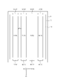
- FIG. 13 is an external view of the thermoelectric conversion module 201 according to the second embodiment of the present invention.
- FIG. 14 is a cross-sectional view of the thermoelectric conversion module 201 along the L2-L2 line shown in FIG.
- FIG. 15 is a cross-sectional view of the thermoelectric conversion module 201 along the L3-L3 line shown in FIG.
- FIG. 16 is a diagram showing the wiring layer 230 shown in FIG. The configuration shown in FIG. 16 corresponds to the configuration after performing the process of forming the wiring layer 230 as shown in FIG. 18 described later.
- FIG. 17 is a diagram showing a current path in the thermoelectric conversion module shown in FIG.
- the thermoelectric conversion module 201 can be arranged in the heat source 2 as in the first embodiment.
- the thermoelectric conversion module 201 includes a first edge portion 201H and a second edge portion 201L in the sheet substrate 210 described later.
- the first edge portion 201H and the second edge portion 201L face each other.
- the first edge portion 201H may be located near the heat source 2 when the thermoelectric conversion module 201 is arranged in the heat source 2, similarly to the first edge portion 1H as shown in FIG.
- the second edge portion 201L may be located away from the heat source 2 when the thermoelectric conversion module 201 is arranged in the heat source 2, similarly to the second edge portion 1L as shown in FIG.
- the temperature near the first edge portion 201H can be higher than the temperature near the second edge portion 201L, similarly to the first edge portion 1H as shown in FIG. In other words, the temperature near the second edge portion 201L can be lower than the temperature near the first edge portion 201H.
- the first direction A1, the second direction A2, and the third direction A3 can be adopted as in the first embodiment.
- the first direction A1 is the direction in which the first edge portion 201H and the second edge portion 201L face each other. It is assumed that the first direction A1 is the direction from the second edge portion 201L toward the first edge portion 201H.
- the third direction A3 is assumed to be a direction from the back side of the paper surface of FIG. 13 toward the front side of the paper surface.
- the shape of the thermoelectric conversion module 201 seen from the third direction A3 is a rectangular shape such as a rectangular shape.
- the thermoelectric conversion module 201 includes a sheet substrate 210, a thermoelectric conversion element 221,222,223,224,225,226,227,228, a wiring layer 230, and a first joining member. It includes 271,272,273,274,275,276,277,278 and a second joining member 281,228,283,284,285,286,287,288.
- the wiring layer 230 is located in the sheet substrate 210.
- the wiring layer 230 may be located on the back surface 212B side of the insulating layer 212 described later. As shown in FIG.
- the wiring layer 230 has a first electrode 241,242, 243, 244, 245, 246, 247, 248 and a second electrode 251, 252, 253, 254, 255, 256, 257, 258. And wirings 261,262,263,264,265,266,267.
- thermoelectric conversion element 220 when each of the thermoelectric conversion elements 221 to 228 is not particularly distinguished, these are collectively referred to as "thermoelectric conversion element 220".
- FIG. 13 shows a thermoelectric conversion module 201 including eight thermoelectric conversion elements 220.
- the number of thermoelectric conversion elements 220 included in the thermoelectric conversion module 201 may be any number.
- first electrode 240 when each of the first electrodes 241 to 248 is not particularly distinguished, these are collectively referred to as “first electrode 240". Further, when each of the second electrodes 251 to 258 is not particularly distinguished, these are collectively referred to as “second electrode 250". Further, when each of the wirings 261 to 267 is not particularly distinguished, these are collectively referred to as "wiring 260".
- FIG. 16 shows a wiring layer 230 having eight first electrodes 240, eight second electrodes 250, and seven wiring 260. However, the number of the first electrode 240, the number of the second electrodes 250, and the number of the wiring 260 of the wiring layer 230 may correspond to the number of the thermoelectric conversion elements 220 included in the thermoelectric conversion module 201.
- FIG. 13 shows a thermoelectric conversion module 201 including eight first joining members 270 and eight second joining members 280.
- the number of the first joining member 270 and the number of the second joining members 280 included in the thermoelectric conversion module 201 may correspond to the number of the thermoelectric conversion elements 220 included in the thermoelectric conversion module 201.
- the numbers An of each of the thermoelectric conversion elements 221,222,223,224,225,226,227,228 are 1, 2, 3, 4, 5, 5, 6, 7, and 8. Become.
- the numbers B n assigned to the first electrodes 241,242, 243, 244, 245, 246, 247, 248 along the second direction A2 are No. 1, No. 2, No. 3, No. 4, No. 5, and No. 6. , 7th and 8th.
- the numbers Cn assigned to the second electrodes 251,252,253,254,255,256,257,258 along the second direction A2 are No. 1, No. 2, No. 3, No. 4, No. 5, and No. 6. , 7th and 8th.
- the numbers Dn assigned to the wirings 261,262,263,264,265,266,267 along the second direction A2 are No. 1, No. 2, No. 3, No. 4, No. 5, No. 6, and No. 7. Become.
- the respective numbers En of the first joining members 271,272 , 273, 274, 275, 276, 277, 278 are No. 1, No. 2, No. 3, No. 4, No. 5, No. 6, and No. 7.
- the numbers F n of the second joining members 281,282, 283, 284, 285, 286, 287, and 288 are No. 1, No. 2, No. 3, No. 4, No. 5, No. 6, and No. 7.
- the sheet substrate 210 has an insulating property.
- the sheet substrate 210 may have flexibility.
- the material for forming the sheet substrate 210 is not particularly limited, and any insulating material can be used.
- the shape of the sheet substrate 210 seen from the third direction A3 is a quadrangle such as a rectangle.
- the sheet substrate 210 includes a first edge portion 201H and a second edge portion 201L.
- the sheet substrate 210 may be parallel to the surface including the first direction A1 and the second direction A2.
- the sheet substrate 210 includes a front surface 210A and a back surface 210B.
- the front surface 210A and the back surface 210B face each other.
- the surface 210A is a surface of the sheet substrate 210 facing the third direction A3.
- the back surface 210B is a surface of the sheet substrate 210 facing in the opposite direction of the third direction A3.
- the sheet substrate 210 has a substrate 211 and an insulating layer 212.
- the substrate 211 has an insulating property.
- the substrate 211 may have flexibility.
- the material of the substrate 211 may be the same as the material of the substrate 11 as shown in FIG.
- the shape of the substrate 11 seen from the third direction A3 is a quadrangle such as a rectangle.
- the substrate 211 may be parallel to the first direction A1 and the second direction A2.
- the substrate 211 includes a front surface 211A and a back surface 211B.
- the front surface 211A and the back surface 211B face each other.
- the surface 211A is a surface of the substrate 211 facing the third direction A3.
- the back surface 211B is a surface of the substrate 211 that faces the opposite direction of the third direction A3.
- the back surface 211B may correspond to the back surface 210B of the sheet substrate 210.
- the substrate 211 includes openings 211a, 211b, 211c, 211d.
- the positions of the openings 211a to 211d as seen from the third direction A3 may correspond to the positions of the first electrodes 242, 244, 246, 248.
- the substrate 211 includes openings 211e, 211f, 211g, 211h.
- each position of the openings 211e to 211h seen from the third direction A3 may correspond to each position of the second electrode 252, 254, 256, 258.
- the shape of the openings 211a to 211h seen from the third direction A3 is a circular shape. However, the shape of the openings 211a to 211h may be any shape.
- the insulating layer 212 has an insulating property.
- the insulating layer 212 may have flexibility.
- the material of the insulating layer 212 may be the same as the material of the insulating layer 12 as shown in FIG.
- the shape of the insulating layer 12 seen from the third direction A3 is a quadrangle such as a rectangle.
- the insulating layer 212 may be parallel to the surface including the first direction A1 and the second direction A2.
- the insulating layer 212 includes a front surface 212A and a back surface 212B.
- the front surface 212A and the back surface 212B face each other.
- the surface 212A is a surface of the insulating layer 212 facing the third direction A3.
- the surface 212A may correspond to the surface 210A of the sheet substrate 210.
- the back surface 212B is a surface of the insulating layer 212 facing the opposite direction of the third direction A3.
- the insulating layer 212 includes openings 212a, 212b, 212c, 212d. As shown in FIG. 13, each position of the openings 212a to 212d seen from the third direction A3 may correspond to each position of the first electrodes 241,243,245,247. As shown in FIG. 15, the insulating layer 212 includes openings 212e, 212f, 212g, 212h. As shown in FIG. 13, each position of the openings 212e to 212h seen from the third direction A3 may correspond to each position of the second electrodes 251,253,255,257.
- the shape of the openings 212a to 212h seen from the third direction A3 is a circular shape. However, the shape of the openings 212a to 212h may be any shape.
- thermoelectric conversion elements 221 to 228 are p-type thermoelectric conversion elements or n-type thermoelectric conversion elements.
- the thermoelectric conversion material for forming the thermoelectric conversion element 220 is not particularly limited, and the thermoelectric conversion material described above in the first embodiment can be used.
- all of the thermoelectric conversion elements 221 to 228 are p-type thermoelectric conversion elements, for example, when the thermoelectric conversion material for forming the thermoelectric conversion element 220 is an organic material such as CNT. It may be there.
- all of the thermoelectric conversion elements 221 to 228 may be formed including CNTs.
- thermoelectric conversion element 220 extends along the first direction A1.
- the shape of the thermoelectric conversion element 220 seen from the third direction A3 is a long shape such as a rectangular shape.
- the longitudinal direction of the thermoelectric conversion element 220 is along the first direction A1.
- the longitudinal direction of the thermoelectric conversion element 220 may be parallel to the first direction A1.
- the thermoelectric conversion elements 221 to 228 may have the same shape.
- the cross-sectional shape of the thermoelectric conversion element 220 may be a thin film.
- thermoelectric conversion elements 220 are formed not only on the front surface 210A of the sheet substrate 210 but also on the back surface 210B of the sheet substrate 210.
- the thermoelectric conversion element 220 having an odd number Ann is formed on the surface 210A.
- thermoelectric conversion elements 221,223,225,227 are formed on the surface 210A.
- the thermoelectric conversion element 220 having the number Ann as the number of corners is formed on the back surface 210B .
- the thermoelectric conversion element 222,224,226,228 is formed on the back surface 210B.
- thermoelectric conversion element 220 having an odd number An may be arranged on the front surface 212A side of the insulating layer 212, and the thermoelectric conversion element 220 having the number Ann as the number of corners may be arranged on the back surface 211B side of the substrate 211.
- thermoelectric conversion element 20 By forming the thermoelectric conversion element 20 on both the front surface 210A and the back surface 210B of the sheet substrate 210 in this way, the density of the thermoelectric conversion element 220 in the thermoelectric conversion module 201 can be increased. By increasing the density of the thermoelectric conversion element 220 in the thermoelectric conversion module 201, the thermoelectric conversion module 201 can be miniaturized.
- thermoelectric conversion elements 221 to 228 are arranged so as to be lined up along the second direction A2.
- the thermoelectric conversion elements 221,223,225,227 may be arranged along the second direction A2 with a gap on the surface 210A of the sheet substrate 210.
- the width of the gap may be arbitrary as long as insulation between two thermoelectric conversion elements 220 adjacent to each other in the second direction A2 can be secured.
- the thermoelectric conversion elements 222, 224, 226, 228 may be arranged along the second direction A2 with a gap on the back surface 210B of the sheet substrate 210.
- the width of the gap may be arbitrary as long as insulation between two thermoelectric conversion elements 220 adjacent to each other in the second direction A2 can be secured.
- thermoelectric conversion module 201 can be miniaturized by having at least a part of each thermoelectric conversion element 220 located on the front surface 210A overlap with at least a part of each thermoelectric conversion element 220 located on the back surface 210B when viewed from the third direction A3. ..
- the thermoelectric conversion module 201 can be miniaturized by having at least a part of each thermoelectric conversion element 220 located on the front surface 210A overlap with at least a part of each thermoelectric conversion element 220 located on the back surface 210B when viewed from the third direction A3. ..
- the thermoelectric conversion element 220 formed on the front surface 210A does not overlap with at least a part of each thermoelectric conversion element 220 formed on the back surface 210B. good.
- the thermoelectric conversion element 220 includes a first end portion 220H and a second end portion 220L in the first direction A1 in the same manner as the thermoelectric conversion element 20 as shown in FIG.
- the first end portion 220H is located toward the first edge portion 201H of the thermoelectric conversion module 201.
- the second end portion 220L is located toward the second edge portion 201L of the thermoelectric conversion module 201.
- the first end 220H of the thermoelectric conversion elements 221 to 228 are “first end 221H”, “first end 222H”, “first end 223H”, “first end 224H", respectively. It is also described as “first end portion 225H”, “first end portion 226H”, “first end portion 227H", and “first end portion 228H”.
- the second end 220L of the thermoelectric conversion elements 221 to 228 are “second end 221L”, “second end 222L”, “second end 223L”, “second end 224L”, respectively. It is also described as “second end portion 225L”, “second end portion 226L”, “second end portion 227L”, and “second end portion 228L”.
- the positions of the first end portions 221H to 228H in the first direction A1 are different. However, the positions of the first end portions 221H to 228H in the first direction A1 may be the same. Further, in the configuration shown in FIG. 1, the positions of the second end portions 221L to 228L in the first direction A1 are different. However, the positions of the second end portions 221L to 228L in the first direction A1 may be the same.
- the positions of the first end portions 222H, 224H, 226H, and 228H in the first direction A1 are the positions of the first end portions 221H, 223H, 225H, and 227H according to the configuration of the wiring layer 230. It may be different from the position in one direction A1 or may be the same.
- thermoelectric conversion element 220 can generate electricity due to a temperature difference between the first end portion 220H and the second end portion 220L.
- a current flowing through the thermoelectric conversion element 220 may be generated.
- the currents I221, I222, I223, I224, I225, I226 flowing through each of the thermoelectric conversion elements 221,222,223,224,225,226,227,228 toward the first direction A1 , I227, I228 can each occur.
- thermoelectric conversion elements 221 to 228 may be rectangular shapes having substantially the same dimensions as described above in the first embodiment. As described above in the first embodiment, the thermoelectric conversion elements 221 to 228 are the first of each of the thermoelectric conversion elements 221 to 228 so that the electric resistance values of the thermoelectric conversion elements 221 to 228 are substantially the same. It may be configured by adjusting the length along the direction A1, the width along the second direction A2 of each of the thermoelectric conversion elements 221 to 228, and the thickness of each of the thermoelectric conversion elements 221 to 228 in the third direction A3.
- the first electrode 240, the second electrode 250, and the wiring 260 may be formed of the same conductive material or may be formed of different conductive materials.
- the conductive material for forming each of the first electrode 240, the second electrode 250, and the wiring 260 is not particularly limited, and any metal such as copper or aluminum can be used.
- any metal such as copper or aluminum can be used.
- it is assumed that the first electrode 240, the second electrode 250, and the wiring 260 are made of the same conductive material.
- the first electrode 240 may be located on the surface 211A of the substrate 211. As shown in FIG. 13, the first electrodes 241 to 248 may be arranged along the second direction A2 with a gap. The width of the gap may be arbitrary as long as the insulation between the two first electrodes 40 adjacent to each other in the second direction A2 can be secured.
- At least a part of the first electrode 240 may be exposed from the sheet substrate 210, that is, the substrate 211 or the insulating layer 212. At least a part of the first electrode 240 exposed from the substrate 211 or the insulating layer 212 may be electrically connected to the first end 220H of the thermoelectric conversion element 220 by the first joining member 270.
- At least a part of the first electrode 240 having an odd number B n may be exposed from the opening of the insulating layer 212.
- at least a part of the first electrode 241 having an odd number B n is exposed from the opening 212a of the insulating layer 212.
- at least a part of the first electrode 243 having an odd number B n is exposed from the opening 212b of the insulating layer 212.
- At least a part of the first electrode 245 having an odd number B n is exposed from the opening 212c of the insulating layer 212.
- At least a part of the first electrode 247 having an odd number B n is exposed from the opening 212d of the insulating layer 212.
- At least a part of the first electrode 240 exposed from the opening of the insulating layer 212 and having an odd number B n is the first end of the thermoelectric conversion element 220 having the same number An as the number B n . It may be electrically connected to the portion 220H by a first joining member 270 having the same number En as the number B n .
- at least a part of each of the first electrodes 241,243,245,247 having an odd number B n is exposed from each of the openings 212a to 212d of the insulating layer 212.
- At least a part of the first electrode 241 exposed from the opening 212a is electrically connected to the first end portion 221H of the first thermoelectric conversion element 221 by the first first joining member 271.
- At least a part of the No. 3 first electrode 243 exposed from the opening 212b is electrically connected to the first end portion 223H of the No. 3 thermoelectric conversion element 223 by the No. 3 first joining member 273.
- At least a part of the No. 5 first electrode 245 exposed from the opening 212c is electrically connected to the first end portion 225H of the No. 5 thermoelectric conversion element 225 by the No. 5 first joining member 275.
- At least a part of the No. 7 first electrode 247 exposed from the opening 212d is electrically connected to the first end portion 227H of the No. 7 thermoelectric conversion element 227 by the No. 7 first joining member 277.
- At least a part of the first electrode 240 having an even number B n may be exposed from the opening of the substrate 211.
- at least a part of the first electrode 242 having an even number B n is exposed from the opening 211a of the substrate 211.
- at least a part of the first electrode 244 having an even number B n is exposed from the opening 211b of the substrate 211.
- at least a part of the first electrode 246 having an even number B n is exposed from the opening 211c of the substrate 211.
- at least a part of the first electrode 248 having an even number B n is exposed from the opening 211d of the substrate 211.
- At least a part of the first electrode 240 whose number B n exposed from the opening of the substrate 211 is an even number is the first end portion of the thermoelectric conversion element 220 having the same number An as the number B n . It may be electrically connected to 220H by a first joining member 270 having the same number En as the number B n .
- a first joining member 270 having the same number En as the number B n .
- at least a part of each of the first electrodes 242, 244, 246, 248 having an even number B n is exposed from each of the openings 211a to 211d of the substrate 211.
- At least a part of the second first electrode 242 exposed from the opening 211a is electrically connected to the first end 222H of the second thermoelectric conversion element 222 by the second first joining member 272.
- At least a part of the No. 4 first electrode 244 exposed from the opening 211b is electrically connected to the first end portion 224H of the No. 4 thermoelectric conversion element 224 by the No. 4 first joining member 274.
- At least a part of the No. 6 first electrode 246 exposed from the opening 211c is electrically connected to the first end portion 226H of the No. 6 thermoelectric conversion element 226 by the No. 6 first joining member 276.
- At least a part of the No. 8 first electrode 248 exposed from the opening 211d is electrically connected to the first end portion 222H of the No. 8 thermoelectric conversion element 228 by the No. 8 first joining member 278.
- the position of the first electrode 240 of the number B n in the second direction A2 may be the same as the position of the thermoelectric conversion element 220 of the same number An as the number B n in the second direction A2. ..
- the first electrode 240 of the number B n may be located closer to the first edge portion 201H of the thermoelectric conversion module 1 than the first end portion 220H of the thermoelectric conversion element 220 of the same number An as the number B n .
- the first electrode 240 of the number B n may be located between the first end 220H and the first edge 201H of the thermoelectric conversion element 220 of the same number An as the number B n .
- each of the first electrodes 241,243,245,247 is located between each of the first ends 221H, 223H, 225H, 227H and the first edge 201H.
- each of the first electrodes 242, 244, 246, and 248 is located between each of the first end portions 222H, 224H, 226H, and 228H and the first edge portion 201H.
- the electric resistance value of the first electrode 240 may be equal to or higher than the electric resistance value of the wiring 260. As described above in the first embodiment, the first electrode 240 may be configured so that the electric resistance value of the first electrode 240 is equal to or higher than the electric resistance value of the wiring 260.
- the take-out wiring for taking out the electric power generated by the thermoelectric conversion module 201 may be electrically connected to any of the plurality of first electrodes 240.
- the take-out wiring may be electrically connected to the first electrode 248.
- the second electrode 250 may be located on the surface 211A of the substrate 211. As shown in FIG. 13, the second electrodes 251 to 258 may be arranged along the second direction A2 with a gap. The width of the gap may be arbitrary as long as the insulation between the two second electrodes 50 adjacent to each other in the second direction A2 can be secured.
- At least a part of the second electrode 250 may be exposed from the sheet substrate 210, that is, the substrate 211 or the insulating layer 12. At least a part of the second electrode 250 exposed from the substrate 211 or the insulating layer 12 may be electrically connected to the second end 220L of the thermoelectric conversion element 220 by the second joining member 280.
- At least a part of the second electrode 250 having an odd number CN may be exposed from the opening of the insulating layer 212.
- at least a part of the second electrode 251 having an odd number C n is exposed from the opening 212e of the insulating layer 212.
- at least a part of the second electrode 253 having an odd number C n is exposed from the opening 212f of the insulating layer 212.
- at least a part of the second electrode 255 having an odd number C n is exposed from the opening 212 g of the insulating layer 212.
- at least a part of the second electrode 257 having an odd number C n is exposed from the opening 212h of the insulating layer 212.
- At least a part of the second electrode 250 exposed from the opening of the insulating layer 212 and having an odd number C n is the second end of the thermoelectric conversion element 220 having the same number An as the number C n . It may be electrically connected to the portion 220L by a second joining member 280 having the same number F n as the number B n .
- at least a part of each of the second electrodes 251,253,255,257 having an odd number Cn is exposed from each of the openings 212e to 212h of the insulating layer 212.
- At least a part of the first second electrode 251 exposed from the opening 212e is electrically connected to the second end portion 221L of the first thermoelectric conversion element 221 by the first second joining member 281.
- At least a part of the third second electrode 253 exposed from the opening 212f is electrically connected to the second end 223L of the third thermoelectric conversion element 223 by the third second joining member 283.
- At least a part of the No. 5 second electrode 255 exposed from the opening 212 g is electrically connected to the second end portion 225L of the No. 5 thermoelectric conversion element 225 by the No. 5 second joining member 285.
- At least a part of the No. 7 second electrode 257 exposed from the opening 212h is electrically connected to the second end portion 227L of the No. 7 thermoelectric conversion element 227 by the No. 7 second joining member 287.
- At least a part of the second electrode 250 having an even number Cn may be exposed from the substrate 211.
- at least a part of the second electrode 252 having an even number C n is exposed from the opening 211e of the substrate 211.
- At least a part of the second electrode 254 having an even number C n is exposed from the opening 211f of the substrate 211.
- At least a part of the second electrode 256 having an even number C n is exposed from the opening 211 g of the substrate 211.
- At least a part of the second electrode 258 having an even number C n is exposed from the opening 211h of the substrate 211.
- At least a part of the second electrode 250 exposed from the opening of the substrate 211 having an even number C n is the second end portion of the thermoelectric conversion element 220 having the same number An as the number C n . It may be electrically connected to 220L by a second joining member 280 having the same number F n as the number B n .
- at least a part of each of the second electrodes 252, 254, 256, 258 having an even number C n is exposed from each of the openings 211e to 211h of the substrate 211.
- At least a part of the second electrode 252 exposed from the opening 211e is electrically connected to the second end 222L of the second thermoelectric conversion element 222 by the second joining member 282.
- At least a part of the No. 4 second electrode 254 exposed from the opening 211f is electrically connected to the second end portion 224L of the No. 4 thermoelectric conversion element 224 by the No. 4 second joining member 284.
- At least a part of the No. 6 second electrode 256 exposed from the opening 211 g is electrically connected to the second end portion 226L of the No. 6 thermoelectric conversion element 226 by the No. 6 second joining member 286.
- At least a part of the second electrode 258 of No. 8 exposed from the opening 211h is electrically connected to the second end portion 228L of the thermoelectric conversion element 228 of No. 8 by the second joining member 288 of No. 8.
- the position of the second electrode 250 of the number C n in the second direction A2 may be the same as the position of the thermoelectric conversion element 220 of the same number An as the number C n in the second direction A2. ..
- the second electrode 250 of the number Cn may be located closer to the second edge portion 201L of the thermoelectric conversion module 1 than the second end portion 220L of the thermoelectric conversion element 220 of the same number An as the number Cn.
- the second electrode 250 of the number Cn may be located between the second end 220L and the second edge 201L of the thermoelectric conversion element 220 of the same number An as the number Cn.
- each of the second electrodes 251,253,255,257 is located between each of the second ends 221L, 223L, 225L, 227L and the second edge 201L. Further, each of the second electrodes 252, 254, 256, 258 is located between each of the second end portions 222L, 224L, 226L, and 228L and the second edge portion 201L.
- the electric resistance value of the second electrode 250 may be equal to or higher than the electric resistance value of the wiring 260. As described above in the first embodiment, the second electrode 250 may be configured so that the electric resistance value of the second electrode 250 is equal to or higher than the electric resistance value of the wiring 260.
- the take-out wiring for taking out the electric power generated by the thermoelectric conversion module 201 may be electrically connected to any of the plurality of second electrodes 250.
- the take-out wiring may be electrically connected to the second electrode 251.
- the wiring 260 may be located in the sheet substrate 210. As shown in FIG. 16, the wiring 260 may be located on the surface 211A of the substrate 211 together with the first electrode 240 and the second electrode 250. The wiring 260 may be located on the back surface 212B side of the insulating layer 212. The wiring 260 may be located on the back surface 212B side of the insulating layer 212 together with the first electrode 240 and the second electrode 250.
- the wiring 260 electrically connects the thermoelectric conversion elements 220 adjacent to each other in the second direction A2 at both ends of the thermoelectric conversion element 220, that is, the first end portion 220H and the second end portion 220L.
- the wiring 260 is a first electrode 240 electrically connected to the first end 220H of one thermoelectric conversion element 220 in two thermoelectric conversion elements 220 adjacent to each other in the second direction A2, and the other.
- the second electrode 250 which is electrically connected to the second end 220L of the thermoelectric conversion element 220, is electrically connected.
- the plurality of wirings 260 are arranged in the order of the numbers Ann assigned to the thermoelectric conversion element 220 by electrically connecting the plurality of first electrodes 240 and the plurality of second electrodes 250.
- a plurality of thermoelectric conversion elements 220 may be electrically connected in series.
- the first electrode 240 of the same number En as the number D n and the second electrode 250 of the number F n + 1 which is one larger than the number D n are electrically connected. good.
- One end of the wiring 260 of the number D n may be connected to the first electrode 240 of the same number En as the number D n .
- the other end of the wiring 260 of the number D n may be electrically connected to the second electrode 250 of the number F n + 1 , which is one larger than the number D n .
- the wiring 260 of the number D n may extend linearly from the first electrode 240 of the same number En as the number D n to the second electrode 250 of the number F n + 1 which is one larger than the number D n .
- one end of the first wiring 261 is electrically connected to the first electrode 241 of the first.
- the other end of the first wiring 261 is electrically connected to the second electrode 252 having a number one larger than that of the first wiring 261.
- One end of the second wiring 262 is electrically connected to the second first electrode 242.
- the other end of the second wire 262 is electrically connected to the third second electrode 253, which has a larger number than the second wire.
- One end of the No. 3 wiring 263 is electrically connected to the No. 3 first electrode 243.
- the other end of the No. 3 wiring 263 is electrically connected to the No. 4 second electrode 254 having a number one larger than that of the No. 3.
- One end of the No. 4 wiring 264 is electrically connected to the No. 4 first electrode 244.
- the other end of the No. 4 wiring 264 is electrically connected to the No. 5 second electrode 255, which has a larger number than the No. 4.
- One end of the No. 5 wiring 265 is electrically connected to the No. 5 first electrode 245.
- the other end of the No. 5 wiring 265 is electrically connected to the No. 6 second electrode 256, which has a larger number than the No. 5.
- One end of the No. 6 wiring 266 is electrically connected to the No. 6 first electrode 246.
- the other end of the No. 6 wiring 266 is electrically connected to the No. 7 second electrode 257, which is one number larger than the No. 6.
- One end of the No. 7 wiring 267 is electrically connected to the No. 7 first electrode 247.
- the other end of the No. 7 wiring 267 is electrically connected to the No. 8 second electrode 258, which is one number larger than the No. 7.
- thermoelectric conversion elements 220 may be connected in series in the order of the numbers Ann assigned to the thermoelectric conversion element 20.
- one current path may be generated in the thermoelectric conversion module 1 as shown in FIG. 17 when the plurality of thermoelectric conversion elements 220 generate electric power.
- each of the currents I261, I262, I263, I264, I265, I266, and I267 is a current flowing through the wiring 261,262,263,264,265,266,267.
- the thermal resistance value of the wiring 260 may be equal to or higher than the thermal resistance value of the thermoelectric conversion element 220. As described above in the first embodiment, the wiring 260 may be configured so that the thermal resistance value of the wiring 60 is equal to or higher than the thermal resistance value of the thermoelectric conversion element 20. Further, the thermal resistance value of the wiring 260 may be equal to or higher than the thermal resistance value of the thermoelectric conversion element 220, and the electric resistance value of the wiring 260 may be equal to or lower than the electrical resistance value of the thermoelectric conversion element 20.
- the thermal resistance value of the wiring 260 is equal to or higher than the thermal resistance value of the thermoelectric conversion element 220, and the electric resistance value of the wiring 260 is equal to or lower than the electrical resistance value of the thermoelectric conversion element 20.
- the wiring 260 may be configured.
- the wiring 160A as shown in FIG. 11 or the wiring 160B as shown in FIG. 12 may be adopted.
- the first joining member 270 has conductivity.
- the first joining member 270 may be formed of any member such as silver paste or solder.
- the first joining member 270 of the number En is the first end 220H of the thermoelectric conversion element 220 having the same number Ann as the number En, and the first end portion 220H having the same number B n as the number En.
- One electrode 240 may be electrically connected.
- the first joining member 270 having an odd number En may be located in the opening of the insulating layer 212.
- the first joining member 270 having an odd number En is the same as the first end 220H of the thermoelectric conversion element 220 having the same number An as the number En and the same as the number En through the opening of the insulating layer 212.
- the first electrode 240 of the number Bn may be electrically connected.
- the first joining member 271 is located in the opening 212a of the insulating layer 212.
- the first joining member 271 electrically connects the first end portion 221H of the thermoelectric conversion element 221 of No. 1 and the first electrode 241 of No. 1 via the opening 212a of the insulating layer 212.
- at least a part of the first joining member 273 of No. 3 is located in the opening 212b of the insulating layer 212.
- the first joining member 273 of No. 3 electrically connects the first end portion 223H of the thermoelectric conversion element 223 of No. 3 and the first electrode 243 of No. 3 via the opening 212b of the insulating layer 212.
- first joining member 275 of No. 5 is located in the opening 212c of the insulating layer 212.
- the first joining member 275 of No. 5 electrically connects the first end portion 225H of the thermoelectric conversion element 225 of No. 5 and the first electrode 245 of No. 5 via the opening 212c of the insulating layer 212.
- at least a part of the first joining member 277 of No. 7 is located in the opening 212d of the insulating layer 212.
- the first joining member 277 of No. 7 electrically connects the first end portion 227H of the thermoelectric conversion element 227 of No. 7 and the first electrode 247 of No. 7 via the opening 212d of the insulating layer 212.
- the first joining member 270 having an even number En may be located in the opening of the substrate 211.
- the first joining member 270 having an even number En is the first end 220H of the thermoelectric conversion element 220 having the same number An as the number En and the same number as the number En through the opening of the substrate 211.
- the first electrode 240 of B n may be electrically connected.
- the first joining member 272 of No. 2 is located in the opening 211a of the substrate 211.
- the second first joining member 272 electrically connects the first end portion 222H of the second thermoelectric conversion element 222 and the second first electrode 242 via the opening 211a of the substrate 211.
- at least a part of the first joining member 274 of No. 4 is located in the opening 211b of the substrate 211.
- the first joining member 274 of No. 4 electrically connects the first end portion 224H of the thermoelectric conversion element 224 of No. 4 and the first electrode 244 of No. 4 via the opening 211b of the substrate 211.
- the No. 6 first joining member 276 electrically connects the first end portion 226H of the No. 6 thermoelectric conversion element 226 and the No. 6 first electrode 246 via the opening 211c of the substrate 211. Further, at least a part of the first joining member 278 of No. 8 is located in the opening 211d of the substrate 211. The first joining member 278 of No. 8 electrically connects the first end portion 228H of the thermoelectric conversion element 228 of No. 8 and the first electrode 248 of No. 8 via the opening 211d of the substrate 211.
- the first joining member 270 may be configured so that the electric resistance value of the first joining member 270 is equal to or higher than the electric resistance value of the wiring 260.
- the second joining member 280 has conductivity.
- the second joining member 280 may be formed of any member such as silver paste or solder.
- the second joining member 280 having the same number F n is the second end 220L of the thermoelectric conversion element 220 having the same number An as the number F n , and the second end portion 220 L having the same number B n as the number F n .
- the two electrodes 250 are electrically connected.
- the second joining member 280 having an odd number F n may be located in the opening of the insulating layer 212.
- the second joining member 280 having an odd number F n is the same as the second end 220L of the thermoelectric conversion element 220 having the same number An as the number F n and the same as the number F n through the opening of the insulating layer 212. It may be electrically connected to the second electrode 250 of the number Bn .
- the first second joining member 281 is located in the opening 212e of the insulating layer 212.
- the first second joining member 281 electrically connects the second end portion 221L of the first thermoelectric conversion element 221 and the first second electrode 251 via the opening 212e of the insulating layer 212. ..
- at least a part of the second joining member 283 of No. 3 is located in the opening 212f of the insulating layer 212.
- the second joining member 283 of No. 3 electrically connects the second end portion 223L of the thermoelectric conversion element 223 of No. 3 and the second electrode 253 of No. 3 via the opening 212f of the insulating layer 212. ..
- the second joining member 285 of No. 5 is located in the opening 212 g of the insulating layer 212.
- the second joining member 285 of No. 5 electrically connects the second end portion 225L of the thermoelectric conversion element 225 of No. 5 and the second electrode 255 of No. 5 via the opening 212 g of the insulating layer 212. ..
- at least a part of the second joining member 287 of No. 7 is located in the opening 212h of the insulating layer 212.
- the second joining member 287 of No. 7 electrically connects the second end portion 227L of the thermoelectric conversion element 227 of No. 7 and the second electrode 257 of No. 7 via the opening 212h of the insulating layer 212. ..
- the second joining member 280 having an even number F n may be located in the opening of the substrate 211.
- the second joining member 280 having an even number F n is the second end 220L of the thermoelectric conversion element 220 having the same number An as the number F n and the same number as the number F n through the opening of the substrate 211.
- the second electrode 250 of B n may be electrically connected.
- the second joining member 282 of No. 2 is located in the opening 211e of the substrate 211.
- the second joining member 282 electrically connects the second end portion 222L of the thermoelectric conversion element 222 of No. 2 and the second electrode 252 of No. 2 via the opening 211e of the substrate 211.
- at least a part of the second joining member 284 of No. 4 is located in the opening 211f of the substrate 211.
- the second joining member 284 of No. 4 electrically connects the second end portion 224L of the thermoelectric conversion element 224 of No. 4 and the second electrode 254 of No. 4 via the opening 211f of the substrate 211.
- the second joining member 286 of No. 6 electrically connects the second end portion 226L of the thermoelectric conversion element 226 of No. 6 and the second electrode 256 of No. 6 via the opening 211 g of the substrate 211. Further, at least a part of the second joining member 288 of No. 8 is located in the opening 211h of the substrate 211. The second joining member 288 of No. 8 electrically connects the second end portion 228L of the thermoelectric conversion element 228 of No. 8 and the second electrode 258 of No. 8 via the opening 211h of the substrate 211.
- the second joining member 280 may be configured so that the electric resistance value of the second joining member 280 is equal to or higher than the electric resistance value of the wiring 260.
- thermoelectric conversion module 201 according to the second embodiment is the same as those of the thermoelectric conversion module 1 according to the first embodiment.
- FIG. 18 is a flowchart showing the flow of the manufacturing method of the thermoelectric conversion module 201 shown in FIG.
- the method for manufacturing the thermoelectric conversion module 201 according to the present embodiment includes an arrangement step S20, a forming step S21, S22, S23, S24, S25, S26, and a connecting step S27, which will be described later. ..
- the manufacturing method of the thermoelectric conversion module 201 according to the present embodiment is not limited to the manufacturing method described below. Note that FIGS. 19 to 23 correspond to the cross-sectional views shown in FIG.
- the arranging step S20 is a step of arranging the metal foil 330 on the substrate 211.
- the metal leaf 330 may be arranged on the surface 211A of the substrate 211. Similar to the arrangement step S10 described in the first embodiment, the metal leaf 330 may be adhered to the surface 211A of the substrate 211 by any adhesive having thermal conductivity.
- the metal leaf 330 may be similar to the metal leaf 130 as shown in FIG.
- the metal foil 330 can become the wiring layer 230 through the formation step S21 or the like described later.
- the forming step S21 is a step of forming the wiring layer 230 on the surface 211A of the substrate 211 as shown in FIG. 16 by patterning the metal foil 330.
- Known photolithography or the like may be used for patterning the metal foil 330.
- the forming step S22 is a step of forming openings 211a, 211b, 211c, 211d of the substrate 211 as shown in FIG. 20 and forming 211e, 211f, 211g, 211h of the substrate 211 as shown in FIG.
- the openings 211a to 211h may be formed by any laser.
- the forming step S23 is a step of forming the insulating layer 212 on the substrate 211 and the wiring layer 230, as shown in FIG. 21.
- the insulating layer 212 may be formed by applying an insulating material on the substrate 211 and the wiring layer 230.
- the sheet substrate 210 is formed by forming the insulating layer 212 on the surface 211A of the substrate 211. That is, the sheet substrate 210 has a substrate 211 and an insulating layer 212 formed on the surface 211A of the substrate 211.
- ⁇ Formation step S24> the openings 212a, 212b, 212c, 212d of the insulating layer 212 are formed as shown in FIG. 22, and the openings 212e, 212f, 212g, 212h of the insulating layer 212 as shown in FIG. 15 are formed. It is a process.
- the openings 212a-212h may be formed by any laser.
- the forming step S25 is a step of forming a thermoelectric conversion element layer on the insulating layer 212 and forming a thermoelectric conversion element layer under the substrate 211.
- the thermoelectric conversion element layer is a layer formed including CNTs.
- the thermoelectric conversion element layer is a CNT sheet 320 and a CNT sheet 321 as shown in FIG. 23.
- the CNT sheets 320 and 321 are formed to include CNTs.
- the forming step S25 is a step of arranging the CNT sheet 320 on the insulating layer 212 and arranging the CNT sheet 321 on the substrate 211.
- the CNT sheet 320 is arranged, for example, on the surface 212A of the insulating layer 212, that is, the surface 210A of the sheet substrate 210.
- the CNT sheet 321 is arranged, for example, on the back surface 211B of the substrate 211, that is, the back surface 210B of the sheet substrate 210.
- the CNT sheet 320 can become the thermoelectric conversion elements 221,223,225,227 after undergoing the formation step S26 and the like described later. Further, the CNT sheet 321 can become a thermoelectric conversion element 222, 224, 226, 228 after undergoing the formation step S26 or the like described later.
- the thermoelectric conversion element 220 is formed as a p-type thermoelectric conversion element, p-type CNT sheets 320 and 321 may be used.
- n-type CNT sheets 320 and 321 may be used.
- each of the CNT sheets 320 and 321 may be adhered to each of the front surface 210A and the back surface 210B of the sheet substrate 210 by an arbitrary adhesive sheet such as an epoxy resin.
- the same CNT sheets 120 as described above in the first embodiment may be used.
- the forming step S26 is a step of cutting the thermoelectric conversion element layer, that is, the CNT sheets 320, 321 in the first direction A1 to form a plurality of thermoelectric conversion elements 20 arranged in the first direction A1.
- the forming step S26 may be carried out using a laser.
- each of the CNT sheets 320 and 321 may be cut along the first direction A1 by the laser.
- each of the CNT sheets 320 and 321 is cut along the first direction A1 by the UV laser, the nanosecond laser, or the femtosecond laser. good.
- connection step S27 the first electrode 240 and the second electrode 250 exposed from the substrate 211 or the insulating layer 212 and the plurality of thermoelectric conversion elements 220 are connected so that all of the plurality of thermoelectric conversion elements 220 are electrically connected in series.
- This is a step of electrically connecting both end portions, that is, the first end portion 20H and the second end portion 20L.
- the first electrode 240 and the second electrode 250 can be said to be both ends of the wiring 260.
- connection step S27 both ends of the wiring 260 exposed from the substrate 211 or the insulating layer 212 and the plurality of thermoelectric conversion elements 220 are connected so that all of the plurality of thermoelectric conversion elements 220 are electrically connected in series. It can also be said to be a process of electrically connecting the first end portion 20H and the second end portion 20L.
- connection step S27 silver paste is applied from the first end 220H of the thermoelectric conversion element 220 to the first electrode 240 exposed from the substrate 211 or the insulating layer 212 as shown in FIG. 13, and FIG. 13 shows.
- This is a step of applying the silver paste from the second end 220L of the thermoelectric conversion element 220 as shown to the second electrode 250 exposed from the substrate 211 or the insulating layer 212.
- connection step S27 silver is formed along the first direction A1 from each of the openings 212a to 212d of the insulating layer 212 as shown in FIG. 14 to the first end 220H of the thermoelectric conversion element 220 having an odd number Ann.
- the paste is applied. A part of these silver pastes is filled in each of the openings 212a to 212d and electrically connected to each of the first electrodes 40 having an odd number B n . After drying, these silver pastes can be the first joining member 270 having an odd number En .
- connection step S27 silver paste is formed along the first direction A1 from each of the openings 211a to 211d of the substrate 211 as shown in FIG. 14 to the first end 220H of the thermoelectric conversion element 220 having an even number Ann. It is applied. A part of these silver pastes is electrically connected to each of the first electrodes 40, which are filled in the openings 211a to 211d and have an even number B n . After drying, these silver pastes can be the first joining member 270 having an even number En .
- connection step S27 silver paste is applied along the first direction A1 from each of the openings 212e to 212h of the insulating layer 212 as shown in FIG. 15 to the second end 220L of the thermoelectric conversion element 220 having an odd number Ann. Is applied. A part of these silver pastes is filled in each of the openings 212e to 212h and electrically connected to each of the second electrodes 50 having an odd number Cn . After drying, these silver pastes can become the second joining member 280 having an odd number F n .
- connection step S27 silver paste is formed along the first direction A1 from each of the openings 211e to 211h of the substrate 211 as shown in FIG. 15 to the second end 220L of the thermoelectric conversion element 220 having an even number Ann. It is applied. A part of these silver pastes is filled in each of the openings 211e to 211h and electrically connected to each of the second electrodes 50 having an even number Cn. After drying, these silver pastes can be the second joining member 280 having an even number F n .
- thermoelectric conversion module 201 According to the second embodiment, other configurations and effects of the method for manufacturing the thermoelectric conversion module 201 according to the second embodiment are the same as the method for manufacturing the thermoelectric conversion module 1 according to the first embodiment.
- FIG. 24 is an external view of the thermoelectric conversion module 401 according to the third embodiment of the present invention.
- the thermoelectric conversion module 401 can be arranged in the heat source 2 as in the first embodiment.
- the thermoelectric conversion module 401 includes a first edge portion 401H and a second edge portion 401L in the sheet substrate 410 described later.
- the first edge portion 401H and the second edge portion 401L face each other.
- the first edge portion 401H may be located near the heat source 2 when the thermoelectric conversion module 401 is arranged in the heat source 2.
- the second edge portion 401L may be located away from the heat source 2 when the thermoelectric conversion module 401 is arranged in the heat source 2.
- the temperature near the first edge portion 401H can be higher than the temperature near the second edge portion 401L, similarly to the first edge portion 1H as shown in FIG. In other words, the temperature near the second edge portion 401L can be lower than the temperature near the first edge portion 401H.
- the first direction A1, the second direction A2, and the third direction A3 can be adopted as in the first embodiment.
- the first direction A1 is the direction in which the first edge portion 401H and the second edge portion 401L face each other.
- the first direction A1 is a direction from the second edge portion 401L toward the first edge portion 401H and is a direction orthogonal to the second edge portion 401L.
- the second direction A2 is assumed to be a direction from the left side of the paper surface of FIG. 24 toward the right side of the paper surface.
- the third direction A3 is assumed to be a direction from the back side of the paper surface to the front side of the paper surface in FIG. 24.
- the shape of the thermoelectric conversion module 401 seen from the third direction A3 is a trapezoidal shape.
- the thermoelectric conversion module 401 includes a side 401A and a side 401B in the sheet substrate 410 described later.
- the side 401A and the side 401B are parallel to each other.
- Sides 401A and 401B correspond to the two bases of the trapezoid.
- the first edge 401H corresponds to one of the two trapezoidal legs.
- the second edge 401L corresponds to the other leg of the two trapezoidal legs.
- the distance in the first direction A1 between the first edge portion 401H and the second edge portion 401L widens along the second direction A2.
- the thermoelectric conversion module 401 includes a sheet substrate 410, a thermoelectric conversion element 421, 422, 423, 424, 425,426, and a wiring layer 430.
- the wiring layer 430 is located in the sheet substrate 410.
- the wiring layer 430 may be located on the back surface side of an insulating layer similar to the insulating layer 12 as shown in FIG. 2 of the sheet substrate 410.
- the wiring layer 430 has wiring 461, wiring 462, wiring 464, wiring 464, and wiring 465.
- the wiring layer 430 may further have a first electrode similar to the first electrode 40 as shown in FIG. 1 and a first electrode similar to the second electrode 50 as shown in FIG.
- the thermoelectric conversion module 401 may include a joining member similar to the first joining member 70 as shown in FIG. 1 and a joining member similar to the second joining member 80 as shown in FIG.
- thermoelectric conversion element 420 when each of the thermoelectric conversion elements 421 to 426 is not particularly distinguished, these are collectively referred to as "thermoelectric conversion element 420".
- FIG. 24 shows a thermoelectric conversion module 401 including six thermoelectric conversion elements 420. However, the number of thermoelectric conversion elements 420 included in the thermoelectric conversion module 401 may be any number.
- FIG. 24 shows a wiring layer 430 having five wirings 460.
- the number of wirings 460 included in the wiring layer 430 may correspond to the number of thermoelectric conversion elements 420 included in the thermoelectric conversion module 401.
- thermoelectric conversion elements 420 included in the thermoelectric conversion module 401 along the second direction A2 are also described as “number An” ( n is an integer).
- number An is an integer.
- the respective numbers of the thermoelectric conversion elements 421, 422, 423, 424, 425, 426 are No. 1, No. 2, No. 3, No. 4, No. 5, and No. 6.
- the numbers assigned to the plurality of wirings 460 of the wiring layer 430 along the second direction A2 are also described as “numbers D n " (n is an integer).
- the numbers Dn assigned to the wirings 461, 462, 464, 464, 465 along the second direction A2 are No. 1, No. 2, No. 3, No. 4, and No. 5.
- the sheet substrate 410 has an insulating property.
- the sheet substrate 410 may have flexibility.
- the shape of the sheet substrate 410 seen from the third direction A3 is trapezoidal.
- the sheet substrate 410 includes the above-mentioned first edge portion 401H, the above-mentioned second edge portion 401L, the above-mentioned side 401A, and the above-mentioned side 401B.
- the sheet substrate 410 includes a front surface 410A and a back surface 410B.
- the front surface 410A and the back surface 410B face each other.
- the surface 410A is a surface of the sheet substrate 410 facing the third direction A3.
- the back surface 410B is a surface of the sheet substrate 410 facing the opposite direction of the third direction A3.
- the sheet substrate 410 may have a substrate similar to the substrate 11 and an insulating layer similar to the insulating layer 12 as in the sheet substrate 10 as shown in FIG.
- thermoelectric conversion elements 421 to 426 are p-type thermoelectric conversion elements or n-type thermoelectric conversion elements.
- the thermoelectric conversion material for forming the thermoelectric conversion element 420 is not particularly limited, and the thermoelectric conversion material described above in the first embodiment can be used.
- all of the thermoelectric conversion elements 421 to 426 are p-type thermoelectric conversion elements, for example, when the thermoelectric conversion material for forming the thermoelectric conversion element 420 is an organic material such as CNT. It may be there.
- all of the thermoelectric conversion elements 421 to 426 may be formed including CNTs.
- the thermoelectric conversion element 420 extends along the first direction A1.
- the shape of the thermoelectric conversion element 420 seen from the third direction A3 side is a long shape such as a rectangular shape.
- the longitudinal direction of the thermoelectric conversion element 420 is along the first direction A1.
- the longitudinal direction of the thermoelectric conversion element 420 may be parallel to the first direction A1.
- the cross-sectional shape of the thermoelectric conversion element 420 may be a thin film.
- the thicknesses of the thermoelectric conversion elements 421 to 426 in the third direction A3 may be substantially the same or may be different. Hereinafter, it is assumed that the thicknesses of the thermoelectric conversion elements 421 to 426 in the third direction A3 are substantially the same.
- the thermoelectric conversion element 420 includes a first end portion 420H and a second end portion 420L in the first direction A1.
- the first end portion 420H is located toward the first edge portion 401H of the thermoelectric conversion module 401.
- the second end portion 420L is located toward the second edge portion 401L of the thermoelectric conversion module 401.
- the first end 420H of the thermoelectric conversion element 421,422,423,424,425,426 is "first end 421H", “first end 422H”, “first end 423H”, respectively. Also referred to as “first end 424H”, “first end 425H” and "first end 426H”.
- thermoelectric conversion element 421, 422, 423, 424, 425, 426 is “second end 421L”, “second end 422L”, “second end 423L”, respectively. It is also described as “second end portion 424L”, “second end portion 425L” and “second end portion 426L”.
- thermoelectric conversion elements 421 to 426 are arranged so as to be arranged along the second direction A2 on the surface 410A of the sheet substrate 410, as in the first embodiment. Similar to the first embodiment, the thermoelectric conversion elements 421 to 426 may be arranged so as to be arranged along the second direction A2 on the surface side of the insulating layer included in the sheet substrate 410. The thermoelectric conversion elements 421 to 426 are arranged along the second direction A2 with a gap. The width of the gap may be arbitrary as long as the insulation between the two thermoelectric conversion elements 420 adjacent to each other in the second direction A2 can be secured. Similar to the first embodiment, the thermoelectric conversion elements 421 to 426 are electrically connected in series by wirings 461 to 465 in the order of the numbers Ann assigned to the thermoelectric conversion element 420.
- thermoelectric conversion elements 421 to 426 have different lengths along the first direction A1.
- each of the thermoelectric conversion elements 421 to 426 extends from the first edge portion 401H to the second edge portion 401L along the first direction A1.
- the first direction of the thermoelectric conversion elements 421 to 426 is in the order of the numbers Ann, that is, in the order of the thermoelectric conversion elements 421 to 426.
- the length in A1 becomes longer.
- each of the thermoelectric conversion elements 421 to 426 extends from the first edge portion 401H to the second edge portion 401L, so that the lengths of the thermoelectric conversion elements 421 to 426 along the first direction A1 are different.
- each of the thermoelectric conversion elements 421 to 426 extends from the first edge portion 401H to the second edge portion 401L along the first direction A1, the temperature difference between both ends of each of the thermoelectric conversion elements 421 to 426 can be increased. .. By increasing the temperature difference between both ends of each of the thermoelectric conversion elements 421 to 426, the generated power of each of the thermoelectric conversion elements 421 to 426 can be increased.
- the width between each of the first end portions 421H to 426H and the first edge portion 401H may be the same. Further, the width between each of the second end portions 421L to 426L and the second edge portion 401L may be the same.
- the width between each of the first end portions 421H to 426H and the first edge portion 401H and the width between each of the second end portions 421L to 426L and the second edge portion 401L are appropriate depending on the manufacturing process and the like. May be set.
- thermoelectric conversion elements 421 to 426 along the first direction A1 when the lengths of the thermoelectric conversion elements 421 to 426 along the first direction A1 are different, the widths of the thermoelectric conversion elements 421 to 426 along the second direction A2 are substantially the same.
- the electric resistance values of the conversion elements 421 to 426 are different. If the electric resistance values of the thermoelectric conversion elements 421 to 426 are different, when the thermoelectric conversion elements 421 to 426 are electrically connected in series, the thermoelectric conversion element 420 having a small electric resistance value may cause the thermoelectric conversion module 401. The current is fixed.
- thermoelectric conversion elements 421 to 426 the widths of the thermoelectric conversion elements 421 to 426 along the second direction A2 are different so that the electric resistance values of the thermoelectric conversion elements 421 to 426 are substantially the same. It is configured in. As an example, in the present embodiment, the lengths of the thermoelectric conversion elements 421 to 426 along the first direction A1 become longer in the order of the numbers Ann , that is, in the order of the thermoelectric conversion elements 421 to 426. In this case, each of the thermoelectric conversion elements 421 to 426 may be configured so that the width along the second direction A2 of each of the thermoelectric conversion elements 421 to 426 becomes wider in the order of the thermoelectric conversion elements 421 to 426.
- the width of the thermoelectric conversion elements 421 to 426 along the second direction A2 may be wider in proportion to the length of each of the thermoelectric conversion elements 421 to 426 along the first direction A1. For example, when the length of the thermoelectric conversion element 426 along the first direction A1 is 1.5 times the length of the thermoelectric conversion element 421 along the first direction A1, the width of the thermoelectric conversion element 426 along the second direction A2. Is 1.5 times the width along the second direction A2 of the thermoelectric conversion element 421. With such a configuration, the electric resistance values of the thermoelectric conversion elements 421 to 426 can be substantially the same.
- thermoelectric conversion elements 421 to 426 When the thicknesses of the thermoelectric conversion elements 421 to 426 in the third direction A3 are different, each of the thermoelectric conversion elements 421 to 426 so that the electric resistance values of the thermoelectric conversion elements 421 to 426 are substantially the same.
- thermoelectric conversion elements 421 to 426 may be configured so that the cross-sectional areas orthogonal to the first direction A1 of the above are different.
- the wiring 460 may be located in the sheet substrate 410 in the same manner as the wiring 60 as shown in FIG.
- the wiring 460 may be located on the back surface side of the insulating layer of the sheet substrate 410, similarly to the wiring 60 as shown in FIG.
- the wiring 460 may be located on the back surface side of the insulating layer of the sheet substrate 410 together with the first electrode and the second electrode of the wiring layer 430.
- the wiring 460 connects the thermoelectric conversion elements 426 adjacent to each other in the second direction A2 to both ends of the thermoelectric conversion element 420, that is, the first end portion 420H and the second end portion 420L. And electrically connect in series. Similar to the wiring 60 as shown in FIG.
- the wiring 460 is electrically connected to the first end portion 420H of one of the thermoelectric conversion elements 420 in the two thermoelectric conversion elements 420 adjacent to each other in the second direction A2.
- the first electrode and the second electrode electrically connected to the second end portion 420L of the other thermoelectric conversion element 420 may be electrically connected.
- the thermal resistance value of the wiring 460 is equal to or higher than the thermal resistance value of the thermoelectric conversion element 420.
- the wiring 460 may be configured so that the thermal resistance value of the wiring 460 is equal to or higher than the thermal resistance value of the thermoelectric conversion element 420. Further, the thermal resistance value of the wiring 460 may be equal to or higher than the thermal resistance value of the thermoelectric conversion element 420, and the electric resistance value of the wiring 460 may be equal to or lower than the electrical resistance value of the thermoelectric conversion element 420.
- the thermal resistance value of the wiring 460 is equal to or higher than the thermal resistance value of the thermoelectric conversion element 420, and the electric resistance value of the wiring 460 is equal to or lower than the electrical resistance value of the thermoelectric conversion element 420.
- the wiring 460 may be configured.
- the wiring 160A as shown in FIG. 11 or the wiring 160B as shown in FIG. 12 may be adopted.
- thermoelectric conversion module 401 a plurality of thermoelectric conversion elements may be formed on the back surface 410B of the sheet substrate 410 as in the second embodiment.
- the plurality of thermoelectric conversion elements formed on the back surface 410B may be configured in the same manner as the plurality of thermoelectric conversion elements 420.
- each of the plurality of thermoelectric conversion elements formed on the back surface 410B may extend from the first edge portion 401H to the second edge portion 401L.
- the plurality of thermoelectric conversion elements on the back surface 410B are the second of each of the plurality of thermoelectric conversion elements so that the electric resistance values of the plurality of thermoelectric conversion elements are substantially the same. It may be configured so that the widths along the direction A2 are different. Further, when the thicknesses of the plurality of thermoelectric conversion elements formed on the back surface 410B in the third direction A3 are different, the plurality of thermoelectric conversion elements have substantially the same electric resistance value. Each of the plurality of thermoelectric conversion elements may be configured so that the cross-sectional areas orthogonal to the first direction A1 of each of the thermoelectric conversion elements are different.
- the shape of the sheet substrate 410 is trapezoidal. Since the shape of the sheet substrate 410 is trapezoidal, the degree of freedom in the place where the thermoelectric conversion module 401 is arranged can be increased.
- thermoelectric conversion module 401 can also be manufactured by the manufacturing method described above in the first embodiment.
- thermoelectric conversion module in which a decrease in generated power is suppressed can be provided.
Landscapes
- Chemical & Material Sciences (AREA)
- Inorganic Chemistry (AREA)
- Engineering & Computer Science (AREA)
- Manufacturing & Machinery (AREA)
- Cooling Or The Like Of Semiconductors Or Solid State Devices (AREA)
Abstract
熱電変換モジュールは、表面及び裏面を有する絶縁性のシート基板と、複数の熱電変換素子と、配線層とを備える。複数の熱電変換素子は、前記シート基板の前記表面において、第1方向に延びる長尺状であり、且つ前記第1方向に交差する第2方向に沿って並ぶように配置されている。配線層は、隣り合う前記熱電変換素子同士を、長尺状の両端部にて電気的に直列接続する配線を複数備える。前記複数の熱電変換素子の全ては、p型熱電変換素子であるか、又はn型熱電変換素子である。前記配線の熱抵抗値は、前記熱電変換素子の熱抵抗値以上である。
Description
本発明は、熱電変換モジュール及び熱電変換モジュールの製造方法に関する。
複数の熱電変換素子を備える熱電変換モジュールが知られている(例えば、特許文献1、特許文献2及び非特許文献1)。熱電変換素子は、両端部間の温度差を利用することにより、熱を電力に変換する素子である。
独立行政法人 産業技術総合研究所、"熱電変換性能の高い導電性高分子薄膜を開発"、産総研プレスリリース、[online]、2012年8月31日、[2020年8月17日検索]、インターネット<https://www.aist.go.jp/aist_j/press_release/pr2012/pr20120831/pr20120831.html>
複数の熱電変換素子を備える熱電変換モジュールでは、複数の熱電変換素子を配線によって電気的に接続されることが求められる。複数の熱電変換素子を配線で接続させると、熱電変換素子の高温側の端部の熱が配線を介して熱電変換素子の低温側の端部に伝達される場合がある。熱電変換素子の高温側の端部の熱が熱電変換素子の低温側の端部に伝達されると、熱電変換素子の両端部間の温度差が小さくなり、熱電変換素子の発電電力が低下する場合がある。
そこで、本発明の目的は、上述した課題を解決し、発電電力の低下が抑制された熱電変換モジュール及び熱電変換モジュールの製造方法を提供することにある。
この発明は、上記課題を有利に解決することを目的とするものであり、本発明の熱電変換装置は、表面及び裏面を有する絶縁性のシート基板と、前記シート基板の前記表面において、第1方向に延びる長尺状であり、且つ前記第1方向に交差する第2方向に沿って並ぶように配置されている、複数の熱電変換素子と、隣り合う前記熱電変換素子同士を、長尺状の両端部にて電気的に直列接続する配線を複数備える配線層と、を備える熱電変換モジュールであって、前記複数の熱電変換素子の全ては、p型熱電変換素子であるか、又はn型熱電変換素子であり、前記配線の熱抵抗値は、前記熱電変換素子の熱抵抗値以上である。このような構成により、熱電変換素子の両端部の温度差が小さくなることが抑制され得る。熱電変換素子の両端部の温度差が小さくなることが抑制されることにより、熱電変換素子の発電電力の低下が抑制され得る。よって、発電電力の低下が抑制された熱電変換モジュールが提供され得る。
ここで、本発明の熱電変換装置において、前記複数の熱電変換素子の全ては、p型熱電変換素子である、ことが好ましい。熱電変換素子を形成する熱電変換材料によっては、p型熱電変換素子の一方がn型熱電変換素子も耐久性が高くなる場合がある。複数の熱電変換素子の全てがp型熱電変換素子であることにより、熱電変換モジュールは、耐久性に優れたものとなり得る。
また、本発明の熱電変換装置において、前記配線の電気抵抗値は、前記熱電変換素子の電気抵抗値以下である、ことが好ましい。このような構成により、熱電変換モジュールを流れる電流が配線の電気抵抗値によって制限されてしまうことが抑制され得る。
また、本発明の熱電変換装置において、前記複数の熱電変換素子の全ては、カーボンナノチューブを含んで形成されている、ことが好ましい。このような構成により、熱電変換モジュールの機械的強度をさらに向上させると共に、熱電変換モジュールを軽量化することができる。
また、本発明の熱電変換装置において、前記複数の熱電変換素子は、前記シート基板の前記表面に加えて、前記裏面にも形成されている、ことが好ましい。このようにシート基板の表面及び裏面の両面に熱電変換素子が形成されていることにより、熱電変換モジュールにおける熱電変換素子の密度が高められ得る。熱電変換モジュールにおける熱電変換素子の密度が高められることにより、熱電変換モジュールが小型化され得る。
また、本発明の熱電変換装置において、前記シート基板を平面視した際に、前記表面に形成されている各前記熱電変換素子の一部は、前記裏面に形成されている各前記熱電変換素子の一部に重なる、ことが好ましい。このような構成により、熱電変換モジュールが小型化され得る。
また、本発明の熱電変換装置において、前記複数の熱電変換素子の全ての各々の形状は、略同寸法の長方形状である、ことが好ましい。このような構成により、熱電変換モジュールが小型化され得る。
また、本発明の熱電変換装置において、前記複数の熱電変換素子は、前記複数の熱電変換素子の各々の電気抵抗値が略同一となるように、前記複数の熱電変換素子の各々の前記第1方向に沿う長さ、前記複数の熱電変換素子の各々の前記第2方向に沿う幅、及び、前記複数の熱電変換素子の各々の厚さを調整して構成されている、ことが好ましい。複数の熱電変換素子の各々の電気抵抗値が同じになることにより、熱電変換モジュールにおける電力損失が低減され得る。
また、本発明の熱電変換装置において、前記複数の熱電変換素子の各々の前記厚さが略同一であり、前記複数の熱電変換素子の各々の前記長さが相違しており、且つ前記複数の熱電変換素子の各々の前記幅が相違している、ことが好ましい。
また、本発明の熱電変換装置において、前記シート基板の形状は、台形状であり、前記シート基板は、台形の2つの脚のうちの一方の脚に対応する第1縁部と、前記2つの脚のうちの他方の脚に対応する第2縁部とを含み、前記第1縁部と前記第2縁部との間の前記第1方向における間隔は、前記第2方向に沿って広がり、前記複数の熱電変換素子は、前記第1方向に沿って前記第1縁部から前記第2縁部まで延びる、ことが好ましい。シート基板の形状が台形状であることにより、熱電変換モジュールを配置する場所の自由度が高まり得る。
この発明は、上記課題を有利に解決することを目的とするものであり、本発明の熱電変換モジュールの製造方法は、表面及び裏面を含む基板と、当該基板の表面に形成されている絶縁層とを有する絶縁性のシート基板と、前記絶縁層の表面の側において、第1方向に延びる長尺状であり、且つ前記第1方向に交差する第2方向に沿って並ぶように配置されている複数の熱電変換素子と、前記絶縁層の裏面の側において、隣り合う前記熱電変換素子同士を、長尺状の両端部にて電気的に直列接続する配線を複数備える配線層と、を備える熱電変換モジュールの製造方法であって、前記基板の表面の上に前記配線層を形成する配線層形成工程と、前記配線層を構成する各配線の両端部のみが露出するように、前記基板及び前記配線層の上に絶縁層を形成する絶縁層形成工程と、前記絶縁層の上に、熱電変換素子層を形成する素子形成工程と、前記熱電変換素子層を第1方向に沿って切断し、前記第1方向に沿って並ぶ複数の熱電変換素子を形成する熱電変換素子形成工程と、複数の熱電変換素子の全てが電気的に直列接続されるように、露出している前記配線の両端部と、前記複数の熱電変換素子の両端部とを接続する接続工程と、を含む。このような製造方法によって、発電電力の低下が抑制された熱電変換モジュールが提供され得る。
また、本発明の熱電変換モジュールの製造方法において、前記熱電変換素子層は、カーボンナノチューブを含んで形成されている層である、ことが好ましい。このような構成により、機械的強度がさらに向上すると共に、軽量化された熱電変換モジュールが製造され得る。
また、本発明の熱電変換モジュールの製造方法において、前記熱電変換素子形成工程は、UVレーザ、ナノ秒レーザ又はフェムト秒レーザを用いて実施される、ことが好ましい。UVレーザ若しくはナノ秒レーザ又はフェムト秒レーザを用いることにより、レーザによる熱の発生が低減され得る。レーザによる熱の発生が低減されることにより、熱電変換素子間の隙間が第2方向において広がることが抑制され、熱電変換モジュールにおける熱電変換素子の密度が高められ得る。
本発明によれば、発電電力の低下が抑制された熱電変換モジュール及び熱電変換モジュールの製造方法が提供され得る。
以下、本発明に係る実施形態について、図面を参照して説明する。各図において共通する構成要素には、同じ符号を付している。
(第1実施形態)
図1は、本発明の第1実施形態に係る熱電変換モジュール1の外観図である。図2は、図1に示すL1-L1線に沿った熱電変換モジュール1の断面図である。図3は、図1に示す配線層30を示す図である。図3に示す構成は、後述の図6に示すような配線層30の形成工程S11を実施した後の構成に対応する。図4は、図1に示す熱電変換モジュールにおける電流経路を示す図である。
図1は、本発明の第1実施形態に係る熱電変換モジュール1の外観図である。図2は、図1に示すL1-L1線に沿った熱電変換モジュール1の断面図である。図3は、図1に示す配線層30を示す図である。図3に示す構成は、後述の図6に示すような配線層30の形成工程S11を実施した後の構成に対応する。図4は、図1に示す熱電変換モジュールにおける電流経路を示す図である。
図1に示すように、熱電変換モジュール1は、熱源2に配置可能である。熱電変換モジュール1は、後述のシート基板10に、第1縁部1Hと、第2縁部1Lとを含む。第1縁部1Hと、第2縁部1Lとは、対向する。第1縁部1Hは、熱電変換モジュール1が熱源2に配置された際、熱源2の近くに位置し得る。第2縁部1Lは、熱電変換モジュール1が熱源2に配置された際、熱源2から離れて位置し得る。
第1縁部1H付近の温度は、第1縁部1Hが第2縁部1Lよりも熱源2の方に位置することにより、第2縁部1L付近の温度よりも高温になり得る。換言すると、第2縁部1L付近の温度は、第1縁部1H付近の温度よりも低温になり得る。
図1において、第1方向A1は、第1縁部1Hと第2縁部1Lとが対向する方向である。本実施形態では、第1方向A1は、熱電変換モジュール1の第2縁部1Lから第1縁部1Hに向かう方向であるものとする。
図1において、第2方向A2は、第1方向A1に直交する方向である。ただし、第2方向A2は、第1方向A1に交差すれば、第1方向A1に直交しなくてもよい。本実施形態では、第2方向A2は、図1の紙面左側から紙面右側に向かう方向であるものとする。
図1において、第3方向A3は、第1方向A1及び第2方向A2を含む平面に直交する方向である。本実施形態では、第3方向A3は、図1の紙面奥側から紙面手前側に向かう方向であるものとする。
以下、「上」とは、特に断りが無い限り、第3方向A3側を指すものとする。また、「下」とは、特に断りが無い限り、第3方向A3の反対方向側を指すものとする。
図1に示すように、第3方向A3から見た熱電変換モジュール1の形状は、長方形状等の四角形状である。図1に示すように、熱電変換モジュール1は、シート基板10と、熱電変換素子21,22,23,24と、第1接合部材71,72,73,74と、第2接合部材81,82,83,84とを備える。図3に示すように、熱電変換モジュール1は、配線層30を備える。配線層30は、シート基板10の中に位置する。配線層30は、後述の絶縁層12の裏面12B側に位置してよい。配線層30は、第1電極41,42,43,44と、第2電極51,52,53,54と、配線61,62,63とを有する。
以下、熱電変換素子21~24の各々を特に区別しない場合、これらは、まとめて「熱電変換素子20」とも記載される。図1には、4つの熱電変換素子20を備える熱電変換モジュール1が示されている。ただし、熱電変換モジュール1が備える複数の熱電変換素子20の数は、任意の数であってよい。
以下、第1電極41~44の各々を特に区別しない場合、これらは、まとめて「第1電極40」とも記載される。また、第2電極51~54の各々特に区別しない場合、これらは、まとめて「第2電極50」とも記載される。また、配線61~63の各々を特に区別しない場合、これらは、まとめて「配線60」とも記載される。図3には、4つの第1電極40と、4つの第2電極50と、3つの配線60とを有する配線層30が示されている。ただし、配線層30が有する第1電極40の数、第2電極50の数及び配線60の数は、熱電変換モジュール1が備える熱電変換素子20の数に応じたものであってよい。
以下、第1接合部材71~74の各々を特に区別しない場合、これらは、まとめて「第1接合部材70」とも記載される。また、第2接合部材81~84の各々を特に区別しない場合、これらは、まとめて「第2接合部材80」とも記載される。図1には、4つの第1接合部材70及び4つの第2接合部材80を備える熱電変換モジュール1が示されている。ただし、熱電変換モジュール1が備える第1接合部材70の数及び第2接合部材80の数は、熱電変換モジュール1が備える熱電変換素子20の数に応じたものであってよい。
以下、熱電変換モジュール1が備える複数の熱電変換素子20に第2方向A2に沿って振った番号は、「番号An」(nは整数)とも記載される。番号Anの最小値(n=1)は、1であるものとする。番号Anは、第2方向A2に沿って1つずつ繰り上がっていくものとする。熱電変換素子21,22,23,24の各々の番号Anは、1番、2番、3番及び4番となる。
以下、配線層30が有する複数の第1電極40に第2方向A2に沿って振った番号は、「番号Bn」(nは整数)とも記載される。番号Bnの最小値(n=1)は、1であるものとする。番号Bnは、第2方向A2に沿って1つずつ繰り上がっていくものとする。第1電極41,42,43,44に第2方向A2に沿って振った番号Bnは、1番、2番、3番及び4番となる。
以下、配線層30が有する複数の第2電極50に第2方向A2に沿って振った番号は、「番号Cn」(nは整数)とも記載される。番号Cnの最小値(n=1)は、1であるものとする。番号Cnは、第2方向A2に沿って1つずつ繰り上がっていくものとする。第2電極51,52,53,54に第2方向A2に沿って振った番号Cnは、1番、2番、3番及び4番となる。
以下、配線層30が有する複数の配線60に第2方向A2に沿って振った番号は、「番号Dn」(nは整数)とも記載される。番号Dnの最小値(n=1)は、1であるものとする。番号Dnは、第2方向A2に沿って1つずつ繰り上がっていくものとする。配線61,62,63に第2方向A2に沿って振った番号Dnは、1番、2番及び3番となる。
以下、熱電変換モジュール1が備える複数の第1接合部材70に第2方向A2に沿って振った番号は、「番号En」(nは整数)とも記載される。番号Enの最小値(n=1)は、1であるものとする。番号Enは、第2方向A2に沿って1つずつ繰り上がっていくものとする。第1接合部材71,72,73,74の各々の番号Enは、1番、2番、3番及び4番となる。
以下、熱電変換モジュール1が備える複数の第2接合部材80に第2方向A2に沿って振った番号は、「番号Fn」(nは整数)とも記載される。番号Fnの最小値(n=1)は、1であるものとする。番号Fnは、第2方向A2に沿って1つずつ繰り上がっていくものとする。第2接合部材81,82,83,84の各々の番号Fnは、1番、2番、3番及び4番となる。
図1に示すようなシート基板10は、絶縁性を有する。シート基板10は、可撓性を有してよい。シート基板10を形成するための材料としては、特に限定されることなく、任意の絶縁材料を用いることができる。第3方向A3から見たシート基板10の形状は、長方形状等の四角形である。シート基板10は、第1方向A1及び第2方向A2を含む面と平行であってよい。
シート基板10は、上述の第1縁部1Hと、上述の第2縁部1Lとを含む。図2に示すように、シート基板10は、表面10A及び裏面10Bを含む。表面10Aと裏面10Bとは、対向する。表面10Aは、シート基板10の面のうち、第3方向A3を向く面である。裏面10Bは、シート基板10の面のうち、第3方向A3の反対方向を向く面である。
図2に示すように、シート基板10は、基板11と、絶縁層12とを有する。
基板11は、絶縁性を有する。基板11は、可撓性を有してよい。基板11を形成するための材料としては、特に限定されることなく、ポリイミド又はエポキシガラス等の任意の材料を用いることができる。図1に示すように、第3方向A3から見た基板11の形状は、長方形状等の四角形状である。基板11は、第1方向A1及び第2方向A2を含む面と平行であってよい。
図2に示すように、基板11は、表面11Aと、裏面11Bとを含む。表面11Aと裏面11Bとは、対向する。表面11Aは、基板11の面のうち、第3方向A3を向く面である。裏面11Bは、基板11の面のうち、第3方向A3の反対方向を向く面である。裏面11Bは、シート基板10の裏面10Bに対応してよい。
絶縁層12は、絶縁性を有する。絶縁層12は、可撓性を有してよい。絶縁層12を形成するための材料としては、特に限定されることなく、任意の絶縁性材料を用いることができる。絶縁層12は、基板11の表面11Aに位置してよい。図1に示すように、第3方向A3から見た絶縁層12の形状は、長方形状等の四角形状である。絶縁層12は、第1方向A1及び第2方向A2を含む面と平行であってよい。
図2に示すように、絶縁層12は、表面12Aと、裏面12Bとを含む。表面12Aと、裏面12Bとは、対向する。表面12Aは、絶縁層12の面のうち、第3方向A3を向く面である。表面12Aは、シート基板10の表面10Aに対応してよい。裏面12Bは、絶縁層12の面のうち、第3方向A3の反対方向を向く面である。
熱電変換素子21~24の全ては、p型熱電変換素子であるか、又はn型熱電変換素子である。ここで、熱電変換素子20を形成する熱電変換材料によっては、p型熱電変換素子及びn型熱電変換素子の一方が他方よりも耐久性が高くなる場合がある。熱電変換モジュール1が備える複数の熱電変換素子20の全てがp型熱電変換素子であるか、又はn型熱電変換素子であることにより、熱電変換モジュール1は、耐久性に優れたものとなり得る。
熱電変換素子20を形成するための熱電変換材料としては、特に限定されることなく、ビスマステルル系化合物、アンチモン系化合物、シリコン系化合物、金属酸化物系化合物、ホイスラー合金系化合物、導電性高分子化合物、導電性繊維、及び、これらの複合材料等を用いることができる。中でも、導電性繊維を用いることが好ましく、カーボンナノチューブ(以下、「CNT」とも称する)等の繊維状の炭素ナノ構造体を用いることがより好ましい。CNTを用いれば、本発明の熱電変換モジュール1の機械的強度をさらに向上させると共に、軽量化することができるからである。さらに、CNTとしては特に限定されることなく、単層CNT及び/又は多層CNTを用いることができるが、CNTは、単層CNTであることが好ましい。単層CNTの方が、熱電特性(ゼーベック係数)が優位である傾向があるからである。なお、単層カーボンナノチューブとしては、CNT製造用の触媒層を表面に有する基材上に、原料化合物及びキャリアガスを供給して、化学的気相成長法(CVD法)によりCNTを合成する際に、系内に微量の酸化剤(触媒賦活物質)を存在させることで、触媒層の触媒活性を飛躍的に向上させるという方法(スーパーグロース法;国際公開第2006/011655号参照)に準じて製造したCNTを用いることができる(以下、かかる方法に準じて製造されたCNTを「SGCNT」と称することがある)。さらにSGCNTは折れ曲がりが多いという特徴を持っている。ここで、CNTは、電子移動による熱伝導性は高いが、フォノン振動による熱伝導性の低下効果も高いと考えられている。しかしながら、SGCNTは、他の一般的な方法に従って製造したCNTよりも折れ曲がりが多いため、フォノン振動が増幅されにくい構造となっており、フォノン振動に起因した熱伝導性の低下を抑制することができる。よって、SGCNTは、他の一般的なCNTと比較して、熱電変換材料としてより優位な材料であり得る。
熱電変換素子21~24の全ては、CNTを含んで形成されていてよい。このような構成により、熱電変換モジュール1の機械的強度をさらに向上させると共に、熱電変換モジュール1を軽量化することができる。
熱電変換素子21~24の全ては、例えば熱電変換素子20を形成するための熱電変換材料がCNT等の有機材料である場合、p型熱電変換素子であってよい。熱電変換材料が有機材料である場合、大気中の酸素及び水分等によって熱電変換素子20が酸化することが熱電変換素子20の特性劣化の主要因となる場合がある。この場合、n型熱電変換素子の方がp型熱電変換素子よりも大気中の酸素及び水分等による酸化の影響を受けやすいため、p型熱電変換素子の方がn型熱電変換素子よりも、耐久性が高くなり得る。例えば熱電変換材料が有機材料である場合、熱電変換モジュール1が備える複数の熱電変換素子20の全てがp型熱電変換素子であることにより、熱電変換モジュール1は、耐久性に優れたものとなり得る。
図1に示すように、熱電変換素子20は、第1方向A1に沿って延びる。第3方向A3から見た熱電変換素子20の形状は、長方形状等の長尺状である。熱電変換素子20の長手方向は、第1方向A1に沿う。熱電変換素子20の長手方向は、第1方向A1に平行であってよい。熱電変換素子21~24の形状は、同じ形状であってよい。図2に示すように、熱電変換素子20の断面形状は、薄膜状であってよい。
図1に示すように、熱電変換素子21~24は、シート基板10の表面10A例えば絶縁層12の表面12Aにおいて、第2方向A2に沿って並ぶように配置されている。例えば、熱電変換素子21~24は、絶縁層12の表面12A側において、第2方向A2に沿って並ぶように配置されている。熱電変換素子21~24は、隙間を空けて第2方向A2に沿って並んでよい。当該隙間の幅は、第2方向A2に隣り合う2つの熱電変換素子20の間の絶縁を確保できれば、任意であってよい。
熱電変換素子21~24の全ての各々の形状は、略同寸法の長方形状であってよい。熱電変換素子21~24の全ての各々の形状が略同寸法の長方形状であることにより、シート基板10の表面10Aに熱電変換素子21~24を効率良く配置させることができる。このような構成により、熱電変換モジュールが小型化され得る。
熱電変換素子20は、第1方向A1において第1端部20H及び第2端部20Lを含む。第1端部20Hは、熱電変換モジュール1の第1縁部1Hの方に位置する。第2端部20Lは、熱電変換モジュール1の第2縁部1Lの方に位置する。なお、熱電変換素子21,22,23,24の第1端部20Hは、各々、「第1端部21H」、「第1端部22H」、「第1端部23H」及び「第1端部24H」とも記載される。また、熱電変換素子21,22,23,24の第2端部20Lは、各々、「第2端部21L」、「第2端部22L」、「第2端部23L」及び「第2端部24L」とも記載される。なお、図1に示す構成では、第1端部21H~24Hの第1方向A1における位置が異なる。ただし、第1端部21H~24Hの第1方向A1における位置は、同じであってよい。また、図1に示す構成では、第2端部21L~24Lの第1方向A1における位置が異なる。ただし、第2端部21L~24Lの第1方向A1における位置は、同じであってよい。
熱電変換素子20は、第1端部20Hと第2端部20Lとの間の温度差を利用することにより、発電し得る。具体的には、熱電変換素子20の第1端部20Hの温度は、第1端部20Hが第2端部20Lよりも第1縁部1Hの方に位置することにより、第2端部20Lの温度よりも高くなり得る。第1端部20Hの温度が第2端部20Lの温度よりも高くなることにより、第1端部20Hと第2端部20Lとの間で温度差が生じ得る。第1端部20Hと第2端部20Lとの間で温度差が生じることにより、熱電変換素子20において温度勾配が生じ得る。この温度勾配に起因するゼーベック効果によって起電力が生じることにより、熱電変換素子20は、発電し得る。
熱電変換素子20が発電すると、熱電変換素子20を流れる電流が生じ得る。例えば、図4に示すように、熱電変換素子21,22,23,24の各々を第1方向A1に向けて流れる電流I21,I22,I23,I24の各々が生じ得る。
熱電変換素子21~24は、熱電変換素子21~24の各々の電気抵抗値が略同一となるように、熱電変換素子21~24の各々の第1方向A1に沿う長さ、熱電変換素子21~24の各々の第2方向A2に沿う幅及び熱電変換素子21~24の各々の第3方向A3における厚さを調整して構成されていてよい。ここで、熱電変換素子21~24の電気抵抗値が異なると、熱電変換素子21~24が電気的に直列接続される場合、電気抵抗値が小さい熱電変換素子20によって熱電変換モジュール1に生じ得る電流が決まってしまう。熱電変換素子21~24の各々の電気抵抗値が略同一となることにより、電気抵抗値が小さい熱電変換素子20によって熱電変換モジュール1に生じ得る電流が決まってしまうことが抑制され得る。このような構成により、熱電変換モジュール1における電力損失が低減され得る。
第1電極40と、第2電極50と、配線60とは、同じ導電性材料で形成されてもよいし、異なる導電性材料で形成されてもよい。第1電極40、第2電極50及び配線60の各々を形成するための導電性材料としては、特に限定されることなく、銅又はアルミニウム等の任意の金属を用いることができる。以下、第1電極40と、第2電極50と、配線60とは、同じ導電性材料で形成されるものとする。
第1電極40は、基板11の表面11Aに位置してよい。第1電極41~44は、隙間を空けて第2方向A2に沿って並んでよい。当該隙間の幅は、第2方向A2に隣り合う2つの第1電極40間の絶縁を確保できれば、任意であってよい。
図1に示すように、第1電極40の少なくとも一部は、シート基板10例えば絶縁層12から露出してよい。シート基板10例えば絶縁層12から露出した第1電極40の少なくとも一部は、熱電変換素子20の第1端部20Hに第1接合部材70によって電気的に接続されてよい。
本実施形態では、絶縁層12から露出した番号Bnの第1電極40の少なくとも一部は、番号Bnと同じ番号Enの第1接合部材70によって、番号Bnと同じ番号Anの熱電変換素子20の第1端部20Hに電気的に接続されてよい。例えば、絶縁層12から露出した1番の第1電極41の少なくとも一部は、1番の第1接合部材71によって、1番の熱電変換素子21の第1端部21Hに電気的に接続される。また、絶縁層12から露出した2番の第1電極42の少なくとも一部は、2番の第1接合部材72によって、2番の熱電変換素子22の第1端部22Hに電気的に接続される。また、絶縁層12から露出した3番の第1電極43の少なくとも一部は、3番の第1接合部材73によって、3番の熱電変換素子23の第1端部23Hに電気的に接続される。また、絶縁層12から露出した4番の第1電極44の少なくとも一部は、4番の第1接合部材74によって、4番の熱電変換素子24の第1端部24Hに電気的に接続される。
番号Bnの第1電極40の第2方向A2における位置は、番号Bnと同じ番号Anの熱電変換素子20の第2方向A2における位置と同じであってよい。番号Bnの第1電極40は、番号Bnと同じ番号Anの熱電変換素子20の第1端部20Hよりも熱電変換モジュール1の第1縁部1Hの方に位置してよい。番号Bnの第1電極40は、番号Bnと同じ番号Anの熱電変換素子20の第1端部20Hと熱電変換モジュール1の第1縁部1Hとの間に位置してよい。例えば、1番の第1電極41は、1番の熱電変換素子21の第1端部21Hと第1縁部1Hとの間に位置する。また、2番の第1電極42は、2番の熱電変換素子22の第1端部22Hと第1縁部1Hとの間に位置する。また、3番の第1電極43は、3番の熱電変換素子23の第1端部23Hと第1縁部1Hとの間に位置する。また、4番の第1電極44は、4番の熱電変換素子24の第1端部24Hと第1縁部1Hとの間に位置する。
第1電極40の電気抵抗値は、配線60の電気抵抗値以上であってよい。第1電極40の電気抵抗値が配線60の電気抵抗値以上となるように、第1電極40は構成されていてよい。一例として、第1電極40の第3方向A3における厚さと配線60の第3方向A3における厚さとが同じである場合、第1電極40の第2方向A2に沿う幅は、配線60の後述の図5に示すような幅W60よりも、広くてよい。このような構成により、第1電極40の電気抵抗値が配線60の電気抵抗値以上になり得る。
複数の第1電極40の何れかには、熱電変換モジュール1が発電した電力を取り出すための取り出し配線が電気的に接続されてよい。一例として、第1電極44に、当該取り出し配線が電気的に接続されてよい。
図3に示すように、第2電極50は、基板11の表面11Aに位置してよい。第2電極51~54は、隙間を空けて第2方向A2に沿って並んでよい。当該隙間の幅は、第2方向A2に隣り合う2つの第2電極50間の絶縁を確保できれば、任意であってよい。
図1に示すように、第2電極50の少なくとも一部は、シート基板10から例えば絶縁層12から露出してよい。シート基板10例えば絶縁層12から露出した第2電極50の少なくとも一部は、熱電変換素子20の第2端部20Lに第1接合部材70によって電気的に接続されてよい。
本実施形態では、絶縁層12から露出した番号Cnの第2電極50少なくとも一部は、番号Cnと同じ番号Fnの第2接合部材80によって、番号Cnと同じ番号Anの熱電変換素子20の第2端部20Lに電気的に接続されてよい。例えば、絶縁層12から露出した1番の第2電極51少なくとも一部は、1番の第2接合部材81によって、1番の熱電変換素子21の第2端部21Lに電気的に接続される。また、絶縁層12から露出した2番の第2電極52少なくとも一部は、2番の第2接合部材82によって、2番の熱電変換素子22の第2端部22Lに電気的に接続される。また、絶縁層12から露出した3番の第2電極53少なくとも一部は、3番の第2接合部材83によって、3番の熱電変換素子23の第2端部23Lに電気的に接続される。また、絶縁層12から露出した4番の第2電極54少なくとも一部は、4番の第2接合部材84によって、4番の熱電変換素子24の第2端部24Lに電気的に接続される。
番号Cnの第2電極50の第2方向A2における位置は、番号Cnと同じ番号Anの熱電変換素子20の第2方向A2における位置と同じであってよい。番号Cnの第2電極50は、番号Cnと同じ番号Anの熱電変換素子20の第2端部20Lよりも熱電変換モジュール1の第2縁部1Lの方に位置してよい。番号Cnの第2電極50は、番号Cnと同じ番号Anの熱電変換素子20の第2端部20Lと熱電変換モジュール1の第2縁部1Lとの間に位置してよい。例えば、1番の第2電極51は、1番の熱電変換素子21の第2端部21Lと第2縁部1Lとの間に位置する。2番の第2電極52は、2番の熱電変換素子22の第2端部22Lと第2縁部1Lとの間に位置する。また、3番の第2電極53は、3番の熱電変換素子23の第2端部23Lと第2縁部1Lとの間に位置する。また、4番の第2電極54は、4番の熱電変換素子24の第2端部24Lと第2縁部1Lとの間に位置する。
第2電極50の電気抵抗値は、配線60の電気抵抗値以上であってよい。第2電極50の電気抵抗値が配線60の電気抵抗値以上となるように、第2電極50は構成されていてよい。一例として、第2電極50の第3方向A3における厚さと配線60の第3方向A3における厚さとが同じである場合、第2電極50の第2方向A2に沿う幅は、後述の図5に示すような幅W60よりも、広くてよい。このような構成により、第2電極50の電気抵抗値が配線60の電気抵抗値以上になり得る。
複数の第2電極50の何れかには、熱電変換モジュール1が発電した電力を取り出すための取り出し配線が電気的に接続されてよい。一例として、第2電極51に、当該取り出し配線が電気的に接続されてよい。
図2に示すように、配線60は、シート基板10の中に位置してよい。図3に示すように、配線60は、第1電極40及び第2電極50と共に、基板11の表面11Aに位置してよい。配線60は、絶縁層12の裏面12B側に位置してよい。配線60は、第1電極40及び第2電極50と共に、絶縁層12の裏面12B側に位置してよい。
配線60は、第2方向A2に隣り合う熱電変換素子20同士を、熱電変換素子20の両端部すなわち第1端部20H及び第2端部20Lにて、電気的に直列接続する。本実施形態では、配線60は、第2方向A2に隣り合う2つの熱電変換素子20において、一方の熱電変換素子20の第1端部20Hに電気的に接続される第1電極40と、他方の熱電変換素子20の第2端部20Lに電気的に接続される第2電極50とを電気的に接続する。
図3に示すように、複数の配線60は、複数の第1電極40と複数の第2電極50とを電気的に接続することにより、熱電変換素子20に振られた番号Anの順番に、複数の熱電変換素子20を電気的に直列接続してよい。一例として、番号Dnの配線60は、番号Dnと同じ番号Enの第1電極40と、番号Dnよりも1つ大きな番号Fn+1の第2電極50とを電気的に接続してよい。番号Dnの配線60の一端は、番号Dnと同じ番号Enの第1電極40に接続されてよい。番号Dnの配線60の他端は、番号Dnよりも1つ大きな番号Fn+1の第2電極50に電気的に接続されてよい。番号Dnの配線60は、番号Dnと同じ番号Enの第1電極40から、番号Dnよりも1つ大きな番号Fn+1の第2電極50まで、直線状に延びてよい。
例えば、1番の配線61の一端は、1番の第1電極41に電気的に接続される。1番の配線61の他端は、1番よりも1つ番号が大きい2番の第2電極52に電気的に接続される。2番の配線62の一端は、2番の第1電極42に電気的に接続される。2番の配線62の他端は、2番よりも1つ番号が大きい3番の第2電極53に電気的に接続される。3番の配線63の一端は、3番の第1電極43に電気的に接続される。3番の配線63の他端は、3番よりも1つ番号が大きい4番の第2電極54に電気的に接続される。
このような構成により、熱電変換素子20に振られた番号Anの順に、複数の熱電変換素子20が電気的に直列接続される。複数の熱電変換素子220が電気的に直列接続されると、複数の熱電変換素子20が発電した際に、図4に示すように、熱電変換モジュール1において1つの電流経路が生じ得る。図4において、電流I61,I62,I63,I64は、配線61,62,63,64を流れる電流である。
第1接合部材70は、導電性を有する。第1接合部材70は、銀ペースト又ははんだ等の任意の部材で形成されていてよい。番号Enの第1接合部材70は、番号Enと同じ番号Anの熱電変換素子20の第1端部20Hと、番号Enと同じ番号Anの第1電極40とを電気的に接続してよい。番号Enの第1接合部材70は、番号Enと同じ番号Anの熱電変換素子20の第1端部20Hから番号Enと同じ番号Anの第1電極40まで第1方向A1に沿って延びてよい。
例えば、1番の第1接合部材71は、1番の熱電変換素子21の第1端部21Hと、1番の第1電極41とを電気的に接続する。1番の第1接合部材71は、1番の熱電変換素子21の第1端部21Hから1番の第1電極41まで第1方向A1に沿って延びる。また、2番の第1接合部材72は、2番の熱電変換素子22の第1端部22Hと、2番の第1電極42とを電気的に接続する。2番の第1接合部材72は、2番の熱電変換素子22の第1端部22Hから2番の第1電極42まで第1方向A1に沿って延びる。また、3番の第1接合部材73は、3番の熱電変換素子23の第1端部23Hと、3番の第1電極43とを電気的に接続する。3番の第1接合部材73は、3番の熱電変換素子23の第1端部23Hから3番の第1電極43まで第1方向A1に沿って延びる。また、4番の第1接合部材74は、4番の熱電変換素子24の第1端部24Hと、4番の第1電極44とを電気的に接続する。4番の第1接合部材74は、4番の熱電変換素子24の第1端部24Hから4番の第1電極44まで第1方向A1に沿って延びる。
第1接合部材70の電気抵抗値は、配線60の電気抵抗値以上であってよい。第1接合部材70の電気抵抗値が配線60の電気抵抗値以上になるように、第1接合部材70は、構成されていてよい。第1接合部材70の材料を適宜選択することにより、第1接合部材70の電気抵抗値が配線60の電気抵抗値以上になるようにしてよい。一例として、配線60の材料が銅である場合、第1接合部材70の材料は、銀ペーストであってよい。
第2接合部材80は、導電性を有する。第2接合部材80は、銀ペースト又ははんだ等の任意の部材で形成されていてよい。番号Fnの第2接合部材80は、番号Fnと同じ番号Anの熱電変換素子20の第2端部20Lと、番号Fnと同じ番号Cnの第2電極50とを電気的に接続してよい。番号Fnの第2接合部材80は、番号Fnと同じ番号Anの熱電変換素子20の第2端部20Lから番号Fnと同じ番号Cnの第2電極50まで第1方向A1に沿って延びてよい。
例えば、1番の第2接合部材81は、1番の熱電変換素子21の第2端部21Lと、1番の第2電極51とを電気的に接続する。1番の第2接合部材81は、1番の熱電変換素子21の第2端部21Lから1番の第2電極51まで第1方向A1に沿って延びる。また、2番の第2接合部材82は、2番の熱電変換素子22の第2端部22Lと、2番の第2電極52とを電気的に接続する。2番の第2接合部材82は、2番の熱電変換素子22の第2端部22Lから2番の第2電極52まで第1方向A1に沿って延びる。また、3番の第2接合部材83は、3番の熱電変換素子23の第2端部23Lと、3番の第2電極53とを電気的に接続する。3番の第2接合部材83は、3番の熱電変換素子23の第2端部23Lから3番の第2電極53まで第1方向A1に沿って延びる。また、4番の第2接合部材84は、4番の熱電変換素子24の第2端部24Lと、4番の第2電極54とを電気的に接続する。4番の第2接合部材84は、4番の熱電変換素子24の第2端部24Lから4番の第2電極54まで第1方向A1に沿って延びる。
第2接合部材80の電気抵抗値は、配線60の電気抵抗値以上であってよい。第2接合部材80の電気抵抗値が配線60の電気抵抗値以上になるように、第2接合部材80は、構成されていてよい。第2接合部材80の材料を適宜選択することにより、第2接合部材80の電気抵抗値が配線60の電気抵抗値以上になるようにしてよい。一例として、配線60の材料が銅である場合、第2接合部材80の材料は、銀ペーストであってよい。
ここで、本実施形態では、配線60の熱抵抗値は、熱電変換素子20の熱抵抗値以上である。図5を参照して以下に説明するように、配線60の熱抵抗値が熱電変換素子20の熱抵抗値以上となるように、配線60は、構成されていてよい。配線60の熱抵抗値が熱電変換素子20の熱抵抗値以上になることにより、熱電変換素子20の第1端部20Hの熱が配線60を介して別の熱電変換素子20の第2端部20Lに伝達されることが抑制され得る。例えば、熱電変換素子21の第1端部21Hの熱が配線61を介して熱電変換素子22の第2端部22Lに伝達されることが抑制され得る。熱電変換素子20の第1端部20Hの熱が別の熱電変換素子20の第2端部20Lに伝達されることが抑制されることにより、熱電変換素子20において第1端部20Hと第2端部20Lとの間の温度差が小さくなることが抑制され得る。第1端部20Hと第2端部20Lとの間の温度差が小さくなることが抑制されることにより、熱電変換素子20の発電電力の低下が抑制され得る。
図5は、熱電変換素子20及び配線60の熱抵抗値の設定を説明する図である。以下、熱電変換素子20の長さ、幅及び厚さは、各々、「長さL20」、「幅W20」及び「厚さT20」とも記載される。長さL20は、図1に示すような熱電変換素子20が第1方向A1に沿う長さである。幅W20は、図1に示すような熱電変換素子20が第2方向A2に沿う幅である。厚さT20は、図2に示すような熱電変換素子20の第3方向A3における厚さである。また、配線60の長さ、幅及び厚さは、各々、「長さL60」、「幅W60」及び「厚さT60」とも記載される。長さL60は、図3に示すような番号Dnの配線60が番号Dnと同じ番号Bnの第1電極40から番号Dnよりも1つ大きな番号Cn+1の第2電極50まで延びる長さである。厚さT60は、図2に示すような配線60の第3方向A3における厚さである。幅W60は、図3に示すような番号Dnの配線60が番号Dnと同じ番号Bnの第1電極40から番号Dnよりも1つ大きな番号Cn+1の第2電極50まで延びる方向と第3方向A3とに直交する方向における、配線60の幅である。
配線60の熱抵抗値が熱電変換素子20の熱抵抗値以上になるように、配線60の長さL60、幅W60及び厚さT60が設定されてよい。この場合、以下の式(1)を満たすように、配線60の長さL60、幅W60及び厚さT60が設定されてよい。
(1/κ20)×{L20/(T20×W20)}≦(1/κ60)×{L60/(T60×W60)}
式(1)
式(1)において、熱伝導率κ20は、熱電変換素子20の熱伝導率である。熱伝導率κ60は、熱電変換素子20の熱伝導率である。
(1/κ20)×{L20/(T20×W20)}≦(1/κ60)×{L60/(T60×W60)}
式(1)
式(1)において、熱伝導率κ20は、熱電変換素子20の熱伝導率である。熱伝導率κ60は、熱電変換素子20の熱伝導率である。
さらに、配線60の熱抵抗値が熱電変換素子20の熱抵抗値以上であり、且つ配線60の電気抵抗値が熱電変換素子20の電気抵抗値以下であってよい。つまり、配線60の熱抵抗値が熱電変換素子20の熱抵抗値以上であり、且つ配線60の電気抵抗値が熱電変換素子20の電気抵抗値以下となるように、配線60は、構成されていてよい。この場合、式(1)を満たしつつ、以下の式(2)を満たすように、配線60の長さL60、幅W60及び厚さT60が設定されてよい。配線60の電気抵抗値が熱電変換素子20の電気抵抗値以下になることにより、図4に示すような熱電変換モジュール1を流れる電流が配線60の電気抵抗値によって制限されてしまうことが抑制され得る。
(1/δ20)×{L20/(T20×W20)}≦(1/δ60)×{L60/(T60×W60)}
式(2)
式(2)において、電気伝導率δ20は、熱電変換素子20の電気伝導率である。電気伝導率δ60は、熱電変換素子20の電気伝導率である。
式(2)
式(2)において、電気伝導率δ20は、熱電変換素子20の電気伝導率である。電気伝導率δ60は、熱電変換素子20の電気伝導率である。
ここで、上記式(1)及び式(2)から分かるように、配線60の熱抵抗値が高くなるほど、配線60の電気抵抗値が高くなり得る。つまり、配線61~63の熱抵抗値が高くなるほど、配線61~63の電気抵抗値が高くなることにより、熱電変換モジュール1の全体の電気抵抗値が高くなり得る。配線61~63の電気抵抗値の合計は、熱電変換モジュール1の全体の電気抵抗値の10%程度になるように設定されてよい。このような構成により、配線61~63の熱抵抗値を高くすることにより配線61~63の電気抵抗値が高くなっても、配線61~63の電気抵抗値の合計は、熱電変換モジュール1の全体の電気抵抗値の設計誤差程度となり得る。
上記式(1)及び式(2)を満たす設定例が図5に示す表にまとめられ得る。図5に示す表では、熱電変換素子20の熱伝導率κ20は15[W/mK]であり、熱電変換素子20の電気伝導率δ20は900[S/cm]である。また、熱電変換素子20の長さL20、幅W20及び高さH20は、各々、15[mm]、1.5[mm]及び50[μm]である。このような構成の熱電変換素子20の熱抵抗値は、13.3[K/W]となる。また、熱電変換素子20の電気抵抗値は、2.222[Ω]となる。
例1では、配線60の材料は、銅である。配線60の材料が銅である場合、配線60の熱伝導率κ60は400[W/mK]となり、配線60の電気伝導率δ60は6×107[S/cm]となる。例1では、配線60の長さL60、幅W60及び厚さT60は、各々、16[mm]、0.15[mm]及び15[μm]と設定される。このような構成の配線60の熱抵抗値は、17.8[K/W]となる。配線60の熱抵抗値の17.8[K/W]は、熱電変換素子20の熱抵抗値の13.3[K/W]よりも大きくなる。また、配線60の電気抵抗値は、0.001[Ω]となる。配線60の電気抵抗値の0.001[Ω]は、熱電変換素子20の電気抵抗値の2.222[Ω]よりも大きくなる。
例2でも、例1と同様に、配線60の材料は、銅である。例2では、配線60の長さL60、幅W60及び厚さT60は、各々、16[mm]、0.15[mm]及び20[μm]と設定される。このような構成の配線60の熱抵抗値は、20[K/W]となる。配線60の熱抵抗値の20[K/W]は、熱電変換素子20の熱抵抗値の13.3[K/W]よりも大きくなる。また、配線60の電気抵抗値は、0.001[Ω]となる。配線60の電気抵抗値の0.001[Ω]は、熱電変換素子20の電気抵抗値の2.222[Ω]よりも大きくなる。
このように熱電変換モジュール1では、配線60の熱抵抗値は、熱電変換素子20の熱抵抗値以上である。このような構成により、上述のように、熱電変換素子20において第1端部20Hと第2端部20Lとの間の温度差が小さくなることが抑制され得る。第1端部20Hと第2端部20Lとの間の温度差が小さくなることが抑制されることにより、熱電変換素子20の発電電力の低下が抑制され得る。よって、本実施形態によれば、発電電力の低下が抑制された熱電変換モジュール1が提供され得る。
(熱電変換モジュールの製造方法)
図6は、図1に示す熱電変換モジュール1の製造方法の流れを示すフローチャートである。図6に示すように、本実施形態に係る熱電変換モジュール1の製造方法は、後述する、配置工程S10と、形成工程S11,S12,S13,S14と、接続工程S15とを含む。ただし、本実施形態に係る熱電変換モジュール1の製造方法は、以下に説明する製造方法に限定されない。
図6は、図1に示す熱電変換モジュール1の製造方法の流れを示すフローチャートである。図6に示すように、本実施形態に係る熱電変換モジュール1の製造方法は、後述する、配置工程S10と、形成工程S11,S12,S13,S14と、接続工程S15とを含む。ただし、本実施形態に係る熱電変換モジュール1の製造方法は、以下に説明する製造方法に限定されない。
<配置工程S10>
配置工程S10は、図7に示すように、基板11に金属箔130を配置する工程である。金属箔130は、基板11の表面11Aに配置されてよい。金属箔130は、熱伝導性を有する任意の接着剤によって、基板11の表面11Aに接着されてよい。金属箔130は、後述の形成工程S11等を経て、配線層30となり得る。金属箔130は、銅又はアルミニウム等の任意の金属箔であってよい。
配置工程S10は、図7に示すように、基板11に金属箔130を配置する工程である。金属箔130は、基板11の表面11Aに配置されてよい。金属箔130は、熱伝導性を有する任意の接着剤によって、基板11の表面11Aに接着されてよい。金属箔130は、後述の形成工程S11等を経て、配線層30となり得る。金属箔130は、銅又はアルミニウム等の任意の金属箔であってよい。
<形成工程S11>
形成工程S11(配線層形成工程)は、金属箔130をパターニングすることにより、図3に示すように基板11の表面11A上に配線層30を形成する工程である。金属箔130のパターニングには、公知のフォトリソグラフィ等が用いられてよい。
形成工程S11(配線層形成工程)は、金属箔130をパターニングすることにより、図3に示すように基板11の表面11A上に配線層30を形成する工程である。金属箔130のパターニングには、公知のフォトリソグラフィ等が用いられてよい。
<形成工程S12>
形成工程S12(絶縁層形成工程)は、図8に示すように、基板11及び配線層30上に絶縁層12を形成する工程である。形成工程S12では、図3に示すような基板11及び配線層30上に絶縁材料を塗布することにより、絶縁層12は、形成されてよい。図8に示すように、形成工程S12では、第1電極40及び第2電極50が露出するように、基板11及び配線層30上に絶縁層12が形成される。第1電極40及び第2電極50は、配線60の両端部とも言える。つまり、形成工程S12は、配線60の両端部のみが絶縁層12から露出するように絶縁層12を基板11及び配線層30上に形成する工程とも言える。シート基板10は、基板11の表面11Aに絶縁層12が形成されることにより、形成される。つまり、シート基板10は、基板11と、基板11の表面11Aに形成されている絶縁層12とを有する。
形成工程S12(絶縁層形成工程)は、図8に示すように、基板11及び配線層30上に絶縁層12を形成する工程である。形成工程S12では、図3に示すような基板11及び配線層30上に絶縁材料を塗布することにより、絶縁層12は、形成されてよい。図8に示すように、形成工程S12では、第1電極40及び第2電極50が露出するように、基板11及び配線層30上に絶縁層12が形成される。第1電極40及び第2電極50は、配線60の両端部とも言える。つまり、形成工程S12は、配線60の両端部のみが絶縁層12から露出するように絶縁層12を基板11及び配線層30上に形成する工程とも言える。シート基板10は、基板11の表面11Aに絶縁層12が形成されることにより、形成される。つまり、シート基板10は、基板11と、基板11の表面11Aに形成されている絶縁層12とを有する。
<形成工程S13>
形成工程S13(素子形成工程)は、絶縁層12上に熱電変換素子層を形成する工程である。熱電変換素子層は、CNTを含んで形成されている層である。熱電変換素子層は、後述の形成工程S16等を経た後、熱電変換素子20になり得る。上述のように、熱電変換素子20を形成するための熱電変換材料にCNTを用いると、熱電変換モジュール1の機械的強度をさらに向上させると共に、軽量化することができる。熱電変換素子層がCNTを含んで形成されていることにより、機械的強度がさらに向上すると共に、軽量化された熱電変換モジュール1が製造され得る。
形成工程S13(素子形成工程)は、絶縁層12上に熱電変換素子層を形成する工程である。熱電変換素子層は、CNTを含んで形成されている層である。熱電変換素子層は、後述の形成工程S16等を経た後、熱電変換素子20になり得る。上述のように、熱電変換素子20を形成するための熱電変換材料にCNTを用いると、熱電変換モジュール1の機械的強度をさらに向上させると共に、軽量化することができる。熱電変換素子層がCNTを含んで形成されていることにより、機械的強度がさらに向上すると共に、軽量化された熱電変換モジュール1が製造され得る。
本実施形態では、熱電変換素子層は、図9に示すようなCNTシート120(カーボンナノチューブシート)であるものとする。CNTシート120は、CNTを含んで形成されている。本実施形態では、形成工程S13は、CNTシート120を絶縁層12に配置する工程となる。CNTシート120は、例えば、絶縁層12の表面12Aすなわちシート基板10の表面10Aに配置されてよい。CNTシート120は、エポキシ樹脂等の任意の接着シートによって、絶縁層12の表面12Aに接着されてよい。
CNTシート120は、後述の形成工程S14等を経た後、熱電変換素子20になり得る。熱電変換素子20をp型熱電変換素子として形成する場合、p型のCNTシート120が用いられてよい。熱電変換素子20をn型熱電変換素子として形成する場合、n型のCNTシート120が用いられてよい。CNTシート120の第3方向A3における厚さは、50[μm]程度であってよい。CNTシート120の厚さが50[μm]程度になることにより、熱電変換素子20の電気的特性が発揮され得る。例えば、熱電変換素子20の電気的特性として熱電変換素子20の発電量が、ある程度確保され得る。
なお、形成工程S13では、CNTシート120の代わりに、CNTの分散液を用いた塗布法によって形成されたCNTの塗布膜が、絶縁層12に配置されてもよい。ただし、CNTの塗布膜では、CNTの分散液を乾燥させる過程でCNTが凝集することにより、CNTの塗布膜の導電性が低下したり、CNTの塗布膜の自立性が低下したりするといった問題が生じ得る。また、塗布法によって厚さが50[μm]のCNTの塗布膜を生成するためには、CNTの分散液にバインダを入れることが求められる。しかしながら、CNTの分散液にバインダを入れると、結果的にCNTの塗布膜の導電性が低下するといった問題が生じ得る。このような問題は、形成工程S13においてCNTシート120を用いることにより、解決され得る。
CNTシート120としては、特に限定されることなく、特願2018-065290号に記載のものを用いることができる。CNTシート120は、複数本の単層CNTが絡み合ってなるバンドルを含んでよい。当該バンドルの太さは、1[μm]以下であってよい。当該バンドルの太さが1[μm]以下となることにより、後述の形成工程S14におけるレーザによる熱電変換素子20の切断面の毛羽立ちが低減され得る。熱電変換素子20の毛羽立ちが低減されることにより、熱電変換素子20の毛羽立ちに起因する短絡が生じることが抑制され得る。
形成工程S13では、CNTシート120の状態に応じては、後述の形成工程S14におけるレーザによるダメージを低減させるために、CNTシート120にカバーとなるシートが配置されてもよいし、又はCNTシート120に樹脂材料が塗布されてもよい。
<形成工程S14>
形成工程S14(熱電変換素子形成工程)は、熱電変換素子層すなわちCNTシート120を第1方向A1に沿って切断し、第1方向A1に並ぶ複数の熱電変換素子20を形成する工程である。CNTシート120を第1方向A1に沿って切断することにより、図10に示すような隙間s1が形成される。隙間s1によって第2方向A2に隣り合う2つの熱電変換素子20が区画され得る。
形成工程S14(熱電変換素子形成工程)は、熱電変換素子層すなわちCNTシート120を第1方向A1に沿って切断し、第1方向A1に並ぶ複数の熱電変換素子20を形成する工程である。CNTシート120を第1方向A1に沿って切断することにより、図10に示すような隙間s1が形成される。隙間s1によって第2方向A2に隣り合う2つの熱電変換素子20が区画され得る。
形成工程S14は、レーザを用いて実施されてよい。形成工程S14では、CNTシート120は、レーザによって第1方向A1に沿って切断されてよい。レーザは、第3方向A3側からCNTシート120に向けて照射されてよい。レーザによってCNTシート120が第1方向A1に沿って切断されることにより、図10に示すような隙間s1が形成され得る。
形成工程S14では、UV(Ultra Violet)レーザ若しくはナノ秒レーザ又はフェムト秒レーザによって、CNTシート120が第1方向A1に沿って切断されてよい。ただし、形成工程S14に用いられるレーザは、これらのレーザに限定されない。形成工程S14では、CNTシート120のみを切断可能な、任意のレーザが用いられてよい。例えば、出力が5[W]のUVレーザが用いられる場合、当該UVレーザは、CNTシート120の隙間s1に対応する箇所を第1方向A1に沿って十回から数十回程度スキャンしてよい。
ここで、CNTシート120の面内方向の熱伝導率は、CNTシート120の厚み方向の熱伝導率の100倍程度となり得る。例えば、CNTシート120の第2方向A2における熱伝導率は、CNTシート120の第3方向A3における熱伝導率の100倍程度となり得る。そのため、形成工程S14においてYAG(Yttrium Aluminum Garnet)レーザ等の加熱レーザを用いると、当該加熱レーザによってCNTシート120を第1方向A1に沿って切断していく際に、隙間s1が第2方向A2において広がってしまう場合がある。CNTシート120の第3方向A3における厚さが50[μm]程度である場合に形成工程S14にて加熱レーザを用いると、隙間s1が第2方向A2において5mm程度広がってしまう場合がある。
これに対し、形成工程S14にてUVレーザ若しくはナノ秒レーザ又はフェムト秒レーザ等のレーザを用いると、レーザによる熱の発生が低減され得る。形成工程S14にてレーザによる熱の発生が低減されることにより、隙間s1が第2方向A2において広がることが抑制され得る。隙間s1が第2方向A2において広がることが抑制されることにより、熱電変換モジュール1における熱電変換素子20の密度が高められ得る。熱電変換モジュール1における熱電変換素子20の密度が高まることにより、熱電変換モジュール1が小型化され得る。
さらに、UVレーザのスポット径は、他のレーザのスポット径よりも、小さくなり得る。例えば、UVレーザのスポット径は、8[μm]程度になり得る。UVレーザのスポット径が小さいことにより、CNTシート120へのUVレーザの焦点が絞られ得る。形成工程S14にてUVレーザを用いる場合、CNTシート120へのUVレーザの焦点が絞られ、さらにUVレーザによる熱の発生が低減されることにより、CNTシート120のパターニングの加工精度が向上され得る。例えば、隙間s1の第2方向A2に沿う幅が0.05[mm]から0.1[mm]程度になり得る。CNTシート120のパターニングの加工精度が向上されることにより、熱電変換モジュール1における熱電変換素子20の密度がより高められ、熱電変換モジュール1がより小型化され得る。
形成工程S14にレーザを用いることにより、レーザによるCNTシート120のパターニングがコンピュータ制御により実施可能になる。このような構成により、形成工程S14が簡便になり得る。
<接続工程S15>
接続工程S15は、複数の熱電変換素子20の全てが電気的に直列接続されるように、絶縁層12から露出する第1電極40及び第2電極50と、複数の熱電変換素子20の両端部すなわち第1端部20H及び第2端部20Lとを電気的に接続する工程である。ここで、第1電極40及び第2電極50は、配線60の両端部とも言える。つまり、接続工程S15は、複数の熱電変換素子20の全てが電気的に直列接続されるように、絶縁層12から露出する配線60の両端部と、複数の熱電変換素子20の両端部とを電気的に接続する工程とも言える。
接続工程S15は、複数の熱電変換素子20の全てが電気的に直列接続されるように、絶縁層12から露出する第1電極40及び第2電極50と、複数の熱電変換素子20の両端部すなわち第1端部20H及び第2端部20Lとを電気的に接続する工程である。ここで、第1電極40及び第2電極50は、配線60の両端部とも言える。つまり、接続工程S15は、複数の熱電変換素子20の全てが電気的に直列接続されるように、絶縁層12から露出する配線60の両端部と、複数の熱電変換素子20の両端部とを電気的に接続する工程とも言える。
本実施形態では、接続工程S15は、図1に示すような熱電変換素子20の第1端部20Hから第1電極40まで銀ペーストを塗布し、且つ熱電変換素子20の第2端部20Lから第2電極50まで銀ペーストを塗布する工程である。
接続工程S15において、第1端部20Hから第1電極40まで銀ペーストが塗布されることにより、熱電変換素子20の第1端部20Hと第1電極40とは、電気的に接続され得る。この銀ペーストは、乾燥後、第1接合部材70となり得る。
接続工程S15において、第2端部20Lから第2電極50まで銀ペーストが塗布されることにより、熱電変換素子20の第2端部20Lと第2電極50とは、電気的に接続され得る。この銀ペーストは、乾燥後、第2接合部材80となり得る。
このように本実施形態に係る熱電変換モジュール1の製造方法では、形成工程S14において、UVレーザ若しくはナノ秒レーザ又はフェムト秒レーザによって、CNTシート120が第1方向A1に沿って切断され得る。このような構成により、上述のように、図10に示すような隙間s1が第2方向A2において広がることが抑制され得る。隙間s1が第2方向A2において広がることが抑制されることにより、熱電変換モジュール1における熱電変換素子20の密度が高められ、熱電変換モジュール1が小型化され得る。
(配線の変形例)
配線60の熱抵抗値を熱電変換素子20の熱抵抗値以上にする構成は、図5を参照して上述した構成に限定されない。
配線60の熱抵抗値を熱電変換素子20の熱抵抗値以上にする構成は、図5を参照して上述した構成に限定されない。
例えば、図11に示すような配線160Aを採用することにより、配線160Aの熱抵抗値が熱電変換素子20の熱抵抗値以上になるようにしてよい。配線160Aは、複数の孔160aを含む。配線160Aの熱抵抗値は、配線160Aが孔160aを含むことにより、孔160aを含まない場合よりも、高くなり得る。配線160Aが含む孔160aの数は、配線160Aの熱抵抗値が熱電変換素子20の熱抵抗値以上となるように、適宜設定されてよい。また、配線160Aが含む孔160aの数は、配線160Aの熱抵抗値が熱電変換素子20の熱抵抗値以上となり、配線160Aの電気抵抗値が熱電変換素子20の電気抵抗値以下になるように、適宜設定されてよい。
例えば、図12に示すような配線160Bを採用することにより、配線160Bの熱抵抗値が熱電変換素子20の熱抵抗値以下になるようにしてよい。配線160Bは、ジグザグ状に延びる。配線160Bがジグザグ状に延びることにより、配線160Bの配線長は、ジグザグ状に延びない場合よりも、長くなり得る。そのため、配線160Bの熱抵抗値は、配線160Bがジグザグ状に延びることにより、ジグザグ状に延びない場合よりも、高くなり得る。配線160Bがジグザグ状に延びる長さは、配線160Bの熱抵抗値が熱電変換素子20の熱抵抗値以上となるように、適宜設定されてよい。配線160Bがジグザグ状に延びる長さは、配線160Bの熱抵抗値が熱電変換素子20の熱抵抗値以上となり、配線160Bの電気抵抗値が熱電変換素子20の電気抵抗値以下になるように、適宜設定されてよい。
(第2実施形態)
図13は、本発明の第2実施形態に係る熱電変換モジュール201の外観図である。図14は、図13に示すL2-L2線に沿った熱電変換モジュール201の断面図である。図15は、図13に示すL3-L3線に沿った熱電変換モジュール201の断面図である。図16は、図14に示す配線層230を示す図である。図16に示す構成は、後述の図18に示すような配線層230の形成工程を実施した後の構成に対応する。図17は、図13に示す熱電変換モジュールにおける電流経路を示す図である。
図13は、本発明の第2実施形態に係る熱電変換モジュール201の外観図である。図14は、図13に示すL2-L2線に沿った熱電変換モジュール201の断面図である。図15は、図13に示すL3-L3線に沿った熱電変換モジュール201の断面図である。図16は、図14に示す配線層230を示す図である。図16に示す構成は、後述の図18に示すような配線層230の形成工程を実施した後の構成に対応する。図17は、図13に示す熱電変換モジュールにおける電流経路を示す図である。
熱電変換モジュール201は、第1実施形態と同様に、熱源2に配置可能である。熱電変換モジュール201は、後述のシート基板210に、第1縁部201Hと、第2縁部201Lとを含む。第1縁部201Hと、第2縁部201Lとは、対向する。第1縁部201Hは、図1に示すような第1縁部1Hと同様に、熱電変換モジュール201が熱源2に配置された際に、熱源2の近くに位置し得る。第2縁部201Lは、図1に示すような第2縁部1Lと同様に、熱電変換モジュール201が熱源2に配置された際に、熱源2から離れて位置し得る。
第1縁部201H付近の温度は、図1に示すような第1縁部1Hと同様に、第2縁部201L付近の温度よりも高温になり得る。換言すると、第2縁部201L付近の温度は、第1縁部201H付近の温度よりも低温になり得る。
第2実施形態でも、第1実施形態と同様に、第1方向A1、第2方向A2及び第3方向A3が採用され得る。第2実施形態では、第1方向A1は、第1縁部201Hと第2縁部201Lとが対向する方向である。第1方向A1は、第2縁部201Lから第1縁部201Hに向かう方向であるものとする。また、本実施形態では、第3方向A3は、図13の紙面奥側から紙面手前側に向かう方向であるものとする。
図13に示すように、第3方向A3から見た熱電変換モジュール201の形状は、長方形状等の四角形状である。図13及び図14に示すように、熱電変換モジュール201は、シート基板210と、熱電変換素子221,222,223,224,225,226,227,228と、配線層230と、第1接合部材271,272,273,274,275,276,277,278と、第2接合部材281,282,283,284,285,286,287,288とを備える。図14に示すように、配線層230は、シート基板210の中に位置する。配線層230は、後述の絶縁層212の裏面212B側に位置してよい。図16に示すように、配線層230は、第1電極241,242,243,244,245,246,247,248と、第2電極251,252,253,254,255,256,257,258と、配線261,262,263,264,265,266,267とを有する。
以下、熱電変換素子221~228の各々を特に区別しない場合、これらは、まとめて「熱電変換素子220」とも記載される。図13には、8つの熱電変換素子220を備える熱電変換モジュール201が示されている。ただし、熱電変換モジュール201が備える熱電変換素子220の数は、任意の数であってよい。
以下、第1電極241~248の各々を特に区別しない場合、これらは、まとめて「第1電極240」とも記載される。また、第2電極251~258の各々を特に区別しない場合、これらは、まとめて「第2電極250」とも記載される。また、配線261~267の各々を特に区別しない場合、これらは、まとめて「配線260」とも記載される。図16には、8つの第1電極240と、8つの第2電極250と、7つの配線260とを有する配線層230が示されている。ただし、配線層230が有する第1電極240の数、第2電極250の数及び配線260の数は、熱電変換モジュール201が備える熱電変換素子220の数に応じたものであってよい。
以下、第1接合部材271~278の各々を特に区別しない場合、これらは、まとめて「第1接合部材270」とも記載される。また、第2接合部材281~288の各々を特に区別しない場合、これらは、まとめて「第2接合部材280」とも記載される。図13には、8つの第1接合部材270及び8つの第2接合部材280を備える熱電変換モジュール201が示されている。ただし、熱電変換モジュール201が備える第1接合部材270の数及び第2接合部材280の数は、熱電変換モジュール201が備える熱電変換素子220の数に応じたものであってよい。
以下、第1実施形態と同様に、熱電変換モジュール201が備える複数の熱電変換素子20に第2方向A2に沿って振った番号は、「番号An」(nは整数)とも記載される。番号Anの最小値(n=1)は、1であるものとする。番号Anは、第2方向A2に沿って1つずつ繰り上がっていくものとする。熱電変換素子221,222,223,224,225,226,227,228の各々の番号Anは、1番、2番、3番、4番、5番、6番、7番及び8番となる。
以下、第1実施形態と同様に、配線層230が有する複数の第1電極240に第2方向A2に沿って振った番号は、「番号Bn」(nは整数)とも記載される。番号Bnの最小値(n=1)は、1であるものとする。番号Bnは、第2方向A2に沿って1つずつ繰り上がっていくものとする。第1電極241,242,243,244,245,246,247,248に第2方向A2に沿って振った番号Bnは、1番、2番、3番、4番、5番、6番、7番及び8番となる。
以下、第1実施形態と同様に、配線層230が有する複数の第2電極250に第2方向A2に沿って振った番号は、「番号Cn」(nは整数)とも記載される。番号Cnの最小値(n=1)は、1であるものとする。番号Cnは、第2方向A2に沿って1つずつ繰り上がっていくものとする。第2電極251,252,253,254,255,256,257,258に第2方向A2に沿って振った番号Cnは、1番、2番、3番、4番、5番、6番、7番及び8番となる。
以下、第1実施形態と同様に、配線層230が有する複数の配線260に第2方向A2に沿って振った番号は、「番号Dn」(nは整数)とも記載される。番号Dnの最小値(n=1)は、1であるものとする。番号Dnは、第2方向A2に沿って1つずつ繰り上がっていくものとする。配線261,262,263,264,265,266,267に第2方向A2に沿って振った番号Dnは、1番、2番、3番、4番、5番、6番及び7番となる。
以下、第1実施形態と同様に、熱電変換モジュール201が備える複数の第1接合部材270に第2方向A2に沿って振った番号は、「番号En」(nは整数)とも記載される。番号Enの最小値(n=1)は、1であるものとする。番号Enは、第2方向A2に沿って1つずつ繰り上がっていくものとする。第1接合部材271,272,273,274,275,276,277,278の各々の番号Enは、1番、2番、3番、4番、5番、6番及び7番となる。
以下、第1実施形態と同様に、熱電変換モジュール201が備える複数の第2接合部材280に第2方向A2に沿って振った番号は、「番号Fn」(nは整数)とも記載される。番号Fnの最小値(n=1)は、1であるものとする。番号Fnは、第2方向A2に沿って1つずつ繰り上がっていくものとする。第2接合部材281,282,283,284,285,286,287,288の各々の番号Fnは、1番、2番、3番、4番、5番、6番及び7番となる。
シート基板210は、絶縁性を有する。シート基板210は、可撓性を有してよい。シート基板210を形成するための材料には、特に限定されることなく、任意の絶縁性材料を用いることができる。第3方向A3から見たシート基板210の形状は、長方形状等の四角形である。シート基板210は、第1縁部201Hと、第2縁部201Lとを含む。シート基板210は、第1方向A1及び第2方向A2を含む面と平行であってよい。
図14に示すように、シート基板210は、表面210A及び裏面210Bを含む。表面210Aと裏面210Bとは、対向する。表面210Aは、シート基板210の面のうち、第3方向A3を向く面である。裏面210Bは、シート基板210の面のうち、第3方向A3の反対方向を向く面である。
図14に示すように、シート基板210は、基板211と、絶縁層212とを有する。
基板211は、絶縁性を有する。基板211は、可撓性を有してよい。基板211の材料は、図2に示すような基板11の材料と同じであってよい。第3方向A3から見た基板11の形状は、長方形状等の四角形である。基板211は、第1方向A1及び第2方向A2と平行であってよい。
基板211は、表面211Aと、裏面211Bとを含む。表面211Aと、裏面211Bとは、対向する。表面211Aは、基板211の面のうち、第3方向A3を向く面である。裏面211Bは、基板211の面のうち、第3方向A3の反対方向を向く面である。裏面211Bは、シート基板210の裏面210Bに対応してよい。
図14に示すように、基板211は、開口部211a,211b,211c,211dを含む。図13に示すように、第3方向A3から見た開口部211a~211dの各々の位置は、第1電極242,244,246,248の位置に対応してよい。図15に示すように、基板211は、開口部211e,211f,211g,211hを含む。図13に示すように、第3方向A3から見た開口部211e~211hの各々の位置は、第2電極252,254,256,258の各々の位置に対応してよい。第3方向A3から見た開口部211a~211hの形状は、円形状である。ただし、開口部211a~211hの形状は、任意の形状であってよい。
絶縁層212は、絶縁性を有する。絶縁層212は、可撓性を有してよい。絶縁層212の材料は、図2に示すような絶縁層12の材料と同じであってよい。第3方向A3から見た絶縁層12の形状は、長方形状等の四角形である。絶縁層212は、第1方向A1及び第2方向A2を含む面と平行であってよい。
絶縁層212は、表面212Aと、裏面212Bとを含む。表面212Aと、裏面212Bとは、対向する。表面212Aは、絶縁層212の面のうち、第3方向A3を向く面である。表面212Aは、シート基板210の表面210Aに対応してよい。裏面212Bは、絶縁層212の面のうち、第3方向A3の反対方向を向く面である。
図14に示すように、絶縁層212は、開口部212a,212b,212c,212dを含む。図13に示すように、第3方向A3から見た開口部212a~212dの各々の位置は、第1電極241,243,245,247の各々の位置に対応してよい。図15に示すように、絶縁層212は、開口部212e,212f,212g,212hを含む。図13に示すように、第3方向A3から見た開口部212e~212hの各々の位置は、第2電極251,253,255,257の各々の位置に対応してよい。第3方向A3から見た開口部212a~212hの形状は、円形状である。ただし、開口部212a~212hの形状は、任意の形状であってよい。
熱電変換素子221~228の全ては、p型熱電変換素子であるか、又はn型熱電変換素子である。熱電変換素子220を形成するための熱電変換材料としては、特に限定されることなく、第1実施形態にて上述した熱電変換材料を用いることができる。第1実施形態にて上述したように、熱電変換素子221~228の全ては、例えば熱電変換素子220を形成するための熱電変換材料がCNT等の有機材料である場合、p型熱電変換素子であってよい。第1実施形態にて上述したように、熱電変換素子221~228の全ては、CNTを含んで形成されていてよい。
図13に示すように、熱電変換素子220は、第1方向A1に沿って延びる。第3方向A3から見た熱電変換素子220の形状は、長方形状等の長尺状である。熱電変換素子220の長手方向は、第1方向A1に沿う。熱電変換素子220の長手方向は、第1方向A1に平行であってよい。熱電変換素子221~228の形状は、同じ形状であってよい。図14及び図15に示すように、熱電変換素子220の断面形状は、薄膜状であってよい。
複数の熱電変換素子220は、シート基板210の表面210Aに加えて、シート基板210の裏面210Bにも形成されている。本実施形態では、番号Anが奇数となる熱電変換素子220が表面210Aに形成されている。例えば、熱電変換素子221,223,225,227が表面210Aに形成されている。また、本実施形態では、番号Anが隅数となる熱電変換素子220が裏面210Bに形成されている。例えば、熱電変換素子222,224,226,228が裏面210Bに形成されている。番号Anが奇数となる熱電変換素子220が絶縁層212の表面212A側に配置され、番号Anが隅数となる熱電変換素子220が基板211の裏面211B側に配置されていてよい。
このようにシート基板210の表面210A及び裏面210Bの両面に熱電変換素子20が形成されていることにより、熱電変換モジュール201における熱電変換素子220の密度が高められ得る。熱電変換モジュール201における熱電変換素子220の密度が高められることにより、熱電変換モジュール201が小型化され得る。
熱電変換素子221~228は、第2方向A2に沿って並ぶように配置されている。本実施形態では、熱電変換素子221,223,225,227は、シート基板210の表面210Aにおいて、隙間を空けて第2方向A2に沿って並んでよい。当該隙間の幅は、第2方向A2に隣り合う2つの熱電変換素子220の間の絶縁を確保できれば、任意であってよい。また、熱電変換素子222,224,226,228は、シート基板210の裏面210Bにおいて、隙間を空けて第2方向A2に沿って並んでよい。当該隙間の幅は、第2方向A2に隣り合う2つの熱電変換素子220の間の絶縁を確保できれば、任意であってよい。
図13に示すようにシート基板210を平面視した際にすなわち第3方向A3から見た際、表面210Aに形成されている各熱電変換素子220の少なくとも一部は、裏面210Bに形成されている各熱電変換素子220の少なくとも一部に重なる。第3方向A3から見て表面210Aに位置する各熱電変換素子220の少なくとも一部が裏面210Bに位置する各熱電変換素子220の少なくとも一部に重なることにより、熱電変換モジュール201が小型化され得る。ただし、第3方向A3から見た際、表面210Aに形成されている各熱電変換素子220の少なくとも一部が裏面210Bに形成されている各熱電変換素子220の少なくとも一部に重ならなくてもよい。
熱電変換素子220は、図1に示すような熱電変換素子20と同様に、第1方向A1において第1端部220H及び第2端部220Lを含む。第1端部220Hは、熱電変換モジュール201の第1縁部201Hの方に位置する。第2端部220Lは、熱電変換モジュール201の第2縁部201Lの方に位置する。なお、熱電変換素子221~228の第1端部220Hは、各々、「第1端部221H」、「第1端部222H」、「第1端部223H」、「第1端部224H」、「第1端部225H」、「第1端部226H」、「第1端部227H」、「第1端部228H」とも記載される。また、熱電変換素子221~228の第2端部220Lは、各々、「第2端部221L」、「第2端部222L」、「第2端部223L」、「第2端部224L」、「第2端部225L」、「第2端部226L」、「第2端部227L」、「第2端部228L」とも記載される。なお、図13に示す構成では、第1端部221H~228Hの第1方向A1における位置が異なる。ただし、第1端部221H~228Hの第1方向A1における位置は、同じであってよい。また、図1に示す構成では、第2端部221L~228Lの第1方向A1における位置が異なる。ただし、第2端部221L~228Lの第1方向A1における位置は、同じであってよい。
第3方向A3から見て、第1端部222H,224H,226H,228Hの第1方向A1における位置は、配線層230の構成に応じて、第1端部221H,223H,225H,227Hの第1方向A1における位置と異なってもよいし、同じであってもよい。
熱電変換素子220は、図1に示すような熱電変換素子20と同様に、第1端部220Hと第2端部220Lとの間で温度差が生じることにより、発電し得る。熱電変換素子220が発電すると、熱電変換素子220を流れる電流が生じ得る。例えば、図17に示すように、熱電変換素子221,222,223,224,225,226,227,228の各々を第1方向A1に向けて流れる電流I221,I222,I223,I224,I225,I226,I227,I228の各々が生じ得る。
熱電変換素子221~228の全ての各々の形状は、第1実施形態にて上述したように、略同寸法の長方形状であってよい。第1実施形態にて上述したように、熱電変換素子221~228は、熱電変換素子221~228の各々の電気抵抗値が略同一となるように、熱電変換素子221~228の各々の第1方向A1に沿う長さ、熱電変換素子221~228の各々の第2方向A2に沿う幅及び熱電変換素子221~228の各々の第3方向A3における厚さを調整して構成されていてよい。
第1電極240と、第2電極250と、配線260とは、同じ導電性材料で形成されてもよいし、異なる導電性材料で形成されてもよい。第1電極240、第2電極250及び配線260の各々を形成するための導電性材料は、特に限定されることなく、銅又はアルミニウム等の任意の金属を用いることができる。以下、第1電極240と、第2電極250と、配線260とは、同じ導電性材料で形成されるものとする。
第1電極240は、基板211の表面211Aに位置してよい。図13に示すように、第1電極241~248は、隙間を空けて第2方向A2に沿って並んでよい。当該隙間の幅は、第2方向A2に隣り合う2つの第1電極40間の絶縁を確保できれば、任意であってよい。
第1電極240の少なくとも一部は、シート基板210すなわち基板211又は絶縁層212から露出してよい。基板211又は絶縁層212から露出した第1電極240の少なくとも一部は、熱電変換素子220の第1端部220Hに、第1接合部材270によって電気的に接続されてよい。
本実施形態では、図14に示すように、番号Bnが奇数となる第1電極240の少なくとも一部が絶縁層212の開口部から露出してよい。例えば、番号Bnが奇数となる第1電極241の少なくとも一部は、絶縁層212の開口部212aのから露出する。また、番号Bnが奇数となる第1電極243の少なくとも一部は、絶縁層212の開口部212bから露出する。番号Bnが奇数となる第1電極245の少なくとも一部は、絶縁層212の開口部212cから露出する。番号Bnが奇数となる第1電極247の少なくとも一部は、絶縁層212の開口部212dから露出する。
図14に示すように、絶縁層212の開口部から露出した番号Bnが奇数となる第1電極240の少なくとも一部は、番号Bnと同じ番号Anの熱電変換素子220の第1端部220Hに、番号Bnと同じ番号Enの第1接合部材270によって、電気的に接続されてよい。例えば、番号Bnが奇数となる第1電極241,243,245,247の各々の少なくとも一部は、絶縁層212の開口部212a~212dの各々から露出する。開口部212aから露出した1番の第1電極241の少なくとも一部は、1番の第1接合部材271によって、1番の熱電変換素子221の第1端部221Hに電気的に接続される。開口部212bから露出した3番の第1電極243の少なくとも一部は、3番の第1接合部材273によって、3番の熱電変換素子223の第1端部223Hに電気的に接続される。開口部212cから露出した5番の第1電極245の少なくとも一部は、5番の第1接合部材275によって、5番の熱電変換素子225の第1端部225Hに電気的に接続される。開口部212dから露出した7番の第1電極247の少なくとも一部は、7番の第1接合部材277によって、7番の熱電変換素子227の第1端部227Hに電気的に接続される。
本実施形態では、図14に示すように、番号Bnが偶数となる第1電極240の少なくとも一部が基板211の開口部から露出してよい。例えば、番号Bnが偶数となる第1電極242の少なくとも一部は、基板211の開口部211aから露出する。また、番号Bnが偶数となる第1電極244の少なくとも一部は、基板211の開口部211bから露出する。また、番号Bnが偶数となる第1電極246の少なくとも一部は、基板211の開口部211cから露出する。また、番号Bnが偶数となる第1電極248の少なくとも一部は、基板211の開口部211dから露出する。
図14に示すように、基板211の開口部から露出した番号Bnが偶数となる第1電極240の少なくとも一部は、番号Bnと同じ番号Anの熱電変換素子220の第1端部220Hに、番号Bnと同じ番号Enの第1接合部材270によって、電気的に接続されてよい。例えば、番号Bnが偶数となる第1電極242,244,246,248の各々の少なくとも一部は、基板211の開口部211a~211dの各々から露出する。開口部211aから露出した2番の第1電極242の少なくとも一部は、2番の第1接合部材272によって、2番の熱電変換素子222の第1端部222Hに電気的に接続される。開口部211bから露出した4番の第1電極244の少なくとも一部は、4番の第1接合部材274によって、4番の熱電変換素子224の第1端部224Hに電気的に接続される。開口部211cから露出した6番の第1電極246の少なくとも一部は、6番の第1接合部材276によって、6番の熱電変換素子226の第1端部226Hに電気的に接続される。開口部211dから露出した8番の第1電極248の少なくとも一部は、8番の第1接合部材278によって、8番の熱電変換素子228の第1端部222Hに電気的に接続される。
図13に示すように、番号Bnの第1電極240の第2方向A2における位置は、番号Bnと同じ番号Anの熱電変換素子220の第2方向A2における位置と同じであってよい。番号Bnの第1電極240は、番号Bnと同じ番号Anの熱電変換素子220の第1端部220Hよりも熱電変換モジュール1の第1縁部201Hの方に位置してよい。番号Bnの第1電極240は、番号Bnと同じ番号Anの熱電変換素子220の第1端部220Hと第1縁部201Hとの間に位置してよい。例えば、第1電極241,243,245,247の各々は、第1端部221H,223H,225H,227Hの各々と第1縁部201Hとの間に位置する。また、第1電極242,244,246,248の各々は、第1端部222H,224H,226H,228Hの各々と第1縁部201Hとの間に位置する。
第1電極240の電気抵抗値は、配線260の電気抵抗値以上であってよい。第1電極240は、第1実施形態にて上述したように、第1電極240の電気抵抗値が配線260の電気抵抗値以上になるように構成されていてよい。
複数の第1電極240の何れかには、第1実施形態にて上述したように、熱電変換モジュール201が発電した電力を取り出すための取り出し配線が電気的に接続されてよい。本実施形態では、第1電極248に、当該取り出し配線が電気的に接続されてよい。
第2電極250は、基板211の表面211Aに位置してよい。図13に示すように、第2電極251~258は、隙間を空けて第2方向A2に沿って並んでよい。当該隙間の幅は、第2方向A2に隣り合う2つの第2電極50間の絶縁を確保できれば、任意であってよい。
第2電極250の少なくとも一部は、シート基板210すなわち基板211又は絶縁層12から露出してよい。基板211又は絶縁層12から露出した第2電極250の少なくとも一部は、第2接合部材280によって、熱電変換素子220の第2端部220Lに電気的に接続されてよい。
本実施形態では、図15に示すように、番号Cnが奇数となる第2電極250の少なくとも一部は、絶縁層212の開口部から露出してよい。例えば、番号Cnが奇数となる第2電極251の少なくとも一部は、絶縁層212の開口部212eから露出する。また、番号Cnが奇数となる第2電極253の少なくとも一部は、絶縁層212の開口部212fから露出する。また、番号Cnが奇数となる第2電極255の少なくとも一部は、絶縁層212の開口部212gから露出する。また、番号Cnが奇数となる第2電極257の少なくとも一部は、絶縁層212の開口部212hから露出する。
図15に示すように、絶縁層212の開口部から露出した番号Cnが奇数となる第2電極250の少なくとも一部は、番号Cnと同じ番号Anの熱電変換素子220の第2端部220Lに、番号Bnと同じ番号Fnの第2接合部材280によって、電気的に接続されてよい。例えば、番号Cnが奇数となる第2電極251,253,255,257の各々の少なくとも一部は、絶縁層212の開口部212e~212hの各々から露出する。開口部212eから露出した1番の第2電極251の少なくとも一部は、1番の第2接合部材281によって、1番の熱電変換素子221の第2端部221Lに電気的に接続される。開口部212fから露出した3番の第2電極253の少なくとも一部は、3番の第2接合部材283によって、3番の熱電変換素子223の第2端部223Lに電気的に接続される。開口部212gから露出した5番の第2電極255の少なくとも一部は、5番の第2接合部材285によって、5番の熱電変換素子225の第2端部225Lに電気的に接続される。開口部212hから露出した7番の第2電極257の少なくとも一部は、7番の第2接合部材287によって、7番の熱電変換素子227の第2端部227Lに電気的に接続される。
本実施形態では、図15に示すように、番号Cnが偶数となる第2電極250の少なくとも一部は、基板211から露出してよい。例えば、番号Cnが偶数となる第2電極252の少なくとも一部は、基板211の開口部211eから露出する。番号Cnが偶数となる第2電極254の少なくとも一部は、基板211の開口部211fから露出する。番号Cnが偶数となる第2電極256の少なくとも一部は、基板211の開口部211gから露出する。番号Cnが偶数となる第2電極258の少なくとも一部は、基板211の開口部211hから露出する。
図15に示すように、基板211の開口部から露出した番号Cnが偶数となる第2電極250の少なくとも一部は、番号Cnと同じ番号Anの熱電変換素子220の第2端部220Lに、番号Bnと同じ番号Fnの第2接合部材280によって、電気的に接続されてよい。例えば、番号Cnが偶数となる第2電極252,254,256,258の各々の少なくとも一部は、基板211の開口部211e~211hの各々から露出する。開口部211eから露出した2番の第2電極252の少なくとも一部は、2番の第2接合部材282によって、2番の熱電変換素子222の第2端部222Lに電気的に接続される。開口部211fから露出した4番の第2電極254の少なくとも一部は、4番の第2接合部材284によって、4番の熱電変換素子224の第2端部224Lに電気的に接続される。開口部211gから露出した6番の第2電極256の少なくとも一部は、6番の第2接合部材286によって、6番の熱電変換素子226の第2端部226Lに電気的に接続される。開口部211hから露出した8番の第2電極258の少なくとも一部は、8番の第2接合部材288によって、8番の熱電変換素子228の第2端部228Lに電気的に接続される。
図13に示すように、番号Cnの第2電極250の第2方向A2における位置は、番号Cnと同じ番号Anの熱電変換素子220の第2方向A2における位置と同じであってよい。番号Cnの第2電極250は、番号Cnと同じ番号Anの熱電変換素子220の第2端部220Lよりも熱電変換モジュール1の第2縁部201Lの方に位置してよい。番号Cnの第2電極250は、番号Cnと同じ番号Anの熱電変換素子220の第2端部220Lと第2縁部201Lとの間に位置してよい。例えば、第2電極251,253,255,257の各々は、第2端部221L,223L,225L,227Lの各々と第2縁部201Lとの間に位置する。また、第2電極252,254,256,258の各々は、第2端部222L,224L,226L,228Lの各々と第2縁部201Lとの間に位置する。
第2電極250の電気抵抗値は、配線260の電気抵抗値以上であってよい。第2電極250は、第1実施形態にて上述したように、第2電極250の電気抵抗値が配線260の電気抵抗値以上になるように構成されていてよい。
複数の第2電極250の何れかには、第1実施形態にて上述したように、熱電変換モジュール201が発電した電力を取り出すための取り出し配線が電気的に接続されてよい。本実施形態では、第2電極251に、当該取り出し配線が電気的に接続されてよい。
図16に示すように、配線260は、シート基板210の中に位置してよい。図16に示すように、配線260は、第1電極240及び第2電極250と共に、基板211の表面211Aに位置してよい。配線260は、絶縁層212の裏面212B側に位置してよい。配線260は、第1電極240及び第2電極250と共に、絶縁層212の裏面212B側に位置してよい。
配線260は、第2方向A2に隣り合う熱電変換素子220同士を、熱電変換素子220の両端部すなわち第1端部220H及び第2端部220Lにて電気的に直列接続する。本実施形態では、配線260は、第2方向A2に隣り合う2つの熱電変換素子220において、一方の熱電変換素子220の第1端部220Hに電気的に接続される第1電極240と、他方の熱電変換素子220の第2端部220Lに電気的に接続される第2電極250とを電気的に接続する。
図16に示すように、複数の配線260は、複数の第1電極240と複数の第2電極250とを電気的に接続することにより、熱電変換素子220に振られた番号Anの順番に、複数の熱電変換素子220を電気的に直列接続してよい。一例として、番号Dnの配線260は、番号Dnと同じ番号Enの第1電極240と、番号Dnよりも1つ大きな番号Fn+1の第2電極250とを電気的に接続してよい。番号Dnの配線260の一端は、番号Dnと同じ番号Enの第1電極240に接続されてよい。番号Dnの配線260の他端は、番号Dnよりも1つ大きな番号Fn+1の第2電極250に電気的に接続されてよい。番号Dnの配線260は、番号Dnと同じ番号Enの第1電極240から、番号Dnよりも1つ大きな番号Fn+1の第2電極250まで、直線状に延びてよい。
例えば、1番の配線261の一端は、1番の第1電極241に電気的に接続される。1番の配線261の他端は、1番よりも1つ番号が大きい2番の第2電極252に電気的に接続される。2番の配線262の一端は、2番の第1電極242に電気的に接続される。2番の配線262の他端は、2番よりも1つ番号が大きい3番の第2電極253に電気的に接続される。3番の配線263の一端は、3番の第1電極243に電気的に接続される。3番の配線263の他端は、3番よりも1つ番号が大きい4番の第2電極254に電気的に接続される。4番の配線264の一端は、4番の第1電極244に電気的に接続される。4番の配線264の他端は、4番よりも1つ番号が大きい5番の第2電極255に電気的に接続される。5番の配線265の一端は、5番の第1電極245に電気的に接続される。5番の配線265の他端は、5番よりも1つ番号が大きい6番の第2電極256に電気的に接続される。6番の配線266の一端は、6番の第1電極246に電気的に接続される。6番の配線266の他端は、6番よりも1つ番号が大きい7番の第2電極257に電気的に接続される。7番の配線267の一端は、7番の第1電極247に電気的に接続される。7番の配線267の他端は、7番よりも1つ番号が大きい8番の第2電極258に電気的に接続される。
このような構成により、熱電変換素子20に振られた番号Anの順に、複数の熱電変換素子220が直列接続され得る。複数の熱電変換素子220が電気的に直列接続されると、複数の熱電変換素子220が発電した際に、図17に示すように、熱電変換モジュール1において1つの電流経路が生じ得る。図17において、電流I261,I262,I263,I264,I265,I266,I267の各々は、配線261,262,263,264,265,266,267を流れる電流である。
配線260の熱抵抗値は、熱電変換素子220の熱抵抗値以上であってよい。第1実施形態にて上述したように、配線60の熱抵抗値が熱電変換素子20の熱抵抗値以上となるように、配線260は、構成されていてよい。また、配線260の熱抵抗値が熱電変換素子220の熱抵抗値以上であり、且つ配線260の電気抵抗値が熱電変換素子20の電気抵抗値以下であってよい。第1実施形態にて上述したように、配線260の熱抵抗値が熱電変換素子220の熱抵抗値以上であり、且つ配線260の電気抵抗値が熱電変換素子20の電気抵抗値以下となるように、配線260は、構成されてよい。なお、配線260の代わりに、図11に示すような配線160A又は図12に示すような配線160Bが採用されてもよい。
第1接合部材270は、導電性を有する。第1接合部材270は、銀ペースト又ははんだ等の任意の部材で形成されていてよい。
第1実施形態と同様に、番号Enの第1接合部材270は、番号Enと同じ番号Anの熱電変換素子220の第1端部220Hと、番号Enと同じ番号Bnの第1電極240とを電気的に接続してよい。
第2実施形態では、図14に示すように、番号Enが奇数となる第1接合部材270の少なくとも一部は、絶縁層212の開口部の中に位置してよい。番号Enが奇数となる第1接合部材270は、絶縁層212の開口部を介して、番号Enと同じ番号Anの熱電変換素子220の第1端部220Hと、番号Enと同じ番号Bnの第1電極240とを電気的に接続してよい。
例えば、1番の第1接合部材271の少なくとも一部は、絶縁層212の開口部212aの中に位置する。1番の第1接合部材271は、絶縁層212の開口部212aを介して1番の熱電変換素子221の第1端部221Hと、1番の第1電極241とを電気的に接続する。また、3番の第1接合部材273の少なくとも一部は、絶縁層212の開口部212bの中に位置する。3番の第1接合部材273は、絶縁層212の開口部212bを介して3番の熱電変換素子223の第1端部223Hと、3番の第1電極243とを電気的に接続する。また、5番の第1接合部材275の少なくとも一部は、絶縁層212の開口部212cの中に位置する。5番の第1接合部材275は、絶縁層212の開口部212cを介して5番の熱電変換素子225の第1端部225Hと、5番の第1電極245とを電気的に接続する。また、7番の第1接合部材277の少なくとも一部は、絶縁層212の開口部212dの中に位置する。7番の第1接合部材277は、絶縁層212の開口部212dを介して7番の熱電変換素子227の第1端部227Hと、7番の第1電極247とを電気的に接続する。
図14に示すように、番号Enが偶数となる第1接合部材270の少なくとも一部は、基板211の開口部の中に位置してよい。番号Enが偶数となる第1接合部材270は、基板211の開口部を介して、番号Enと同じ番号Anの熱電変換素子220の第1端部220Hと、番号Enと同じ番号Bnの第1電極240とを電気的に接続してよい。
例えば、2番の第1接合部材272の少なくとも一部は、基板211の開口部211aの中に位置する。2番の第1接合部材272は、基板211の開口部211aを介して、2番の熱電変換素子222の第1端部222Hと、2番の第1電極242とを電気的に接続する。また、4番の第1接合部材274の少なくとも一部は、基板211の開口部211bの中に位置する。4番の第1接合部材274は、基板211の開口部211bを介して、4番の熱電変換素子224の第1端部224Hと、4番の第1電極244とを電気的に接続する。また、6番の第1接合部材276の少なくとも一部は、基板211の開口部211cの中に位置する。6番の第1接合部材276は、基板211の開口部211cを介して、6番の熱電変換素子226の第1端部226Hと、6番の第1電極246とを電気的に接続する。また、8番の第1接合部材278の少なくとも一部は、基板211の開口部211dの中に位置する。8番の第1接合部材278は、基板211の開口部211dを介して、8番の熱電変換素子228の第1端部228Hと、8番の第1電極248とを電気的に接続する。
第1接合部材270は、第1実施形態にて上述したように、第1接合部材270の電気抵抗値が配線260の電気抵抗値以上になるように構成されていてよい。
第2接合部材280は、導電性を有する。第2接合部材280は、銀ペースト又ははんだ等の任意の部材で形成されていてよい。
第1実施形態と同様に、番号Fnの第2接合部材280は、番号Fnと同じ番号Anの熱電変換素子220の第2端部220Lと、番号Fnと同じ番号Bnの第2電極250とを電気的に接続する。
第2実施形態では、図15に示すように、番号Fnが奇数となる第2接合部材280の少なくとも一部は、絶縁層212の開口部の中に位置してよい。番号Fnが奇数となる第2接合部材280は、絶縁層212の開口部を介して、番号Fnと同じ番号Anの熱電変換素子220の第2端部220Lと、番号Fnと同じ番号Bnの第2電極250とを電気的に接続してよい。
例えば、1番の第2接合部材281の少なくとも一部は、絶縁層212の開口部212eの中に位置する。1番の第2接合部材281は、絶縁層212の開口部212eを介して、1番の熱電変換素子221の第2端部221Lと、1番の第2電極251とを電気的に接続する。また、3番の第2接合部材283の少なくとも一部は、絶縁層212の開口部212fの中に位置する。3番の第2接合部材283は、絶縁層212の開口部212fを介して、3番の熱電変換素子223の第2端部223Lと、3番の第2電極253とを電気的に接続する。また、5番の第2接合部材285の少なくとも一部は、絶縁層212の開口部212gの中に位置する。5番の第2接合部材285は、絶縁層212の開口部212gを介して、5番の熱電変換素子225の第2端部225Lと、5番の第2電極255とを電気的に接続する。また、7番の第2接合部材287の少なくとも一部は、絶縁層212の開口部212hの中に位置する。7番の第2接合部材287は、絶縁層212の開口部212hを介して、7番の熱電変換素子227の第2端部227Lと、7番の第2電極257とを電気的に接続する。
第2実施形態では、図15に示すように、番号Fnが偶数となる第2接合部材280の少なくとも一部は、基板211の開口部の中に位置してよい。番号Fnが偶数となる第2接合部材280は、基板211の開口部を介して、番号Fnと同じ番号Anの熱電変換素子220の第2端部220Lと、番号Fnと同じ番号Bnの第2電極250とを電気的に接続してよい。
例えば、2番の第2接合部材282の少なくとも一部は、基板211の開口部211eの中に位置する。2番の第2接合部材282は、基板211の開口部211eを介して、2番の熱電変換素子222の第2端部222Lと、2番の第2電極252とを電気的に接続する。また、4番の第2接合部材284の少なくとも一部は、基板211の開口部211fの中に位置する。4番の第2接合部材284は、基板211の開口部211fを介して、4番の熱電変換素子224の第2端部224Lと、4番の第2電極254とを電気的に接続する。また、6番の第2接合部材286の少なくとも一部は、基板211の開口部211gの中に位置する。6番の第2接合部材286は、基板211の開口部211gを介して、6番の熱電変換素子226の第2端部226Lと、6番の第2電極256とを電気的に接続する。また、8番の第2接合部材288の少なくとも一部は、基板211の開口部211hの中に位置する。8番の第2接合部材288は、基板211の開口部211hを介して、8番の熱電変換素子228の第2端部228Lと、8番の第2電極258とを電気的に接続する。
第2接合部材280は、第1実施形態にて上述したように、第2接合部材280の電気抵抗値が配線260の電気抵抗値以上になるように構成されていてよい。
第2実施形態に係る熱電変換モジュール201のその他の構成及び効果は、第1実施形態に係る熱電変換モジュール1と同様である。
(熱電変換モジュールの製造方法)
図18は、図13に示す熱電変換モジュール201の製造方法の流れを示すフローチャートである。図13に示すように、本実施形態に係る熱電変換モジュール201の製造方法は、後述する、配置工程S20と、形成工程S21,S22,S23,S24,S25,S26と、接続工程S27とを含む。ただし、本実施形態に係る熱電変換モジュール201の製造方法は、以下に説明する製造方法に限定されない。なお、図19から図23は、図14に示す断面図に相当する。
図18は、図13に示す熱電変換モジュール201の製造方法の流れを示すフローチャートである。図13に示すように、本実施形態に係る熱電変換モジュール201の製造方法は、後述する、配置工程S20と、形成工程S21,S22,S23,S24,S25,S26と、接続工程S27とを含む。ただし、本実施形態に係る熱電変換モジュール201の製造方法は、以下に説明する製造方法に限定されない。なお、図19から図23は、図14に示す断面図に相当する。
<配置工程S20>
配置工程S20は、図19に示すように、基板211に金属箔330を配置する工程である。金属箔330は、基板211の表面211Aに配置されてよい。第1実施形態にて説明した配置工程S10と同様に、熱伝導性を有する任意の接着剤によって、金属箔330は、基板211の表面211Aに接着されてよい。金属箔330は、図7に示すような金属箔130と同様のものであってよい。金属箔330は、後述の形成工程S21等を経て、配線層230となり得る。
配置工程S20は、図19に示すように、基板211に金属箔330を配置する工程である。金属箔330は、基板211の表面211Aに配置されてよい。第1実施形態にて説明した配置工程S10と同様に、熱伝導性を有する任意の接着剤によって、金属箔330は、基板211の表面211Aに接着されてよい。金属箔330は、図7に示すような金属箔130と同様のものであってよい。金属箔330は、後述の形成工程S21等を経て、配線層230となり得る。
<形成工程S21>
形成工程S21(配線層形成工程)は、金属箔330をパターニングすることにより、図16に示すような基板211の表面211A上に配線層230を形成する工程である。金属箔330のパターニングには、公知のフォトリソグラフィ等が用いられてよい。
形成工程S21(配線層形成工程)は、金属箔330をパターニングすることにより、図16に示すような基板211の表面211A上に配線層230を形成する工程である。金属箔330のパターニングには、公知のフォトリソグラフィ等が用いられてよい。
<形成工程S22>
形成工程S22は、図20に示すように基板211の開口部211a,211b,211c,211dを形成し、図15に示すような基板211の211e,211f,211g,211hを形成する工程である。任意のレーザによって、開口部211a~211hが形成されてよい。
形成工程S22は、図20に示すように基板211の開口部211a,211b,211c,211dを形成し、図15に示すような基板211の211e,211f,211g,211hを形成する工程である。任意のレーザによって、開口部211a~211hが形成されてよい。
<形成工程S23>
形成工程S23(絶縁層形成工程)は、図21に示すように、基板211及び配線層230上に絶縁層212を形成する工程である。形成工程S23では、基板211及び配線層230上に絶縁材料を塗布することにより、絶縁層212が形成されてよい。シート基板210は、基板211の表面211Aに絶縁層212が形成されることにより、形成される。つまり、シート基板210は、基板211と、基板211の表面211Aに形成されている絶縁層212とを有する。
形成工程S23(絶縁層形成工程)は、図21に示すように、基板211及び配線層230上に絶縁層212を形成する工程である。形成工程S23では、基板211及び配線層230上に絶縁材料を塗布することにより、絶縁層212が形成されてよい。シート基板210は、基板211の表面211Aに絶縁層212が形成されることにより、形成される。つまり、シート基板210は、基板211と、基板211の表面211Aに形成されている絶縁層212とを有する。
<形成工程S24>
形成工程S24では、図22に示すように絶縁層212の開口部212a,212b,212c,212dを形成し、図15に示すような絶縁層212の開口部212e,212f,212g,212hを形成する工程である。任意のレーザによって、開口部212a~212hが形成されてよい。
形成工程S24では、図22に示すように絶縁層212の開口部212a,212b,212c,212dを形成し、図15に示すような絶縁層212の開口部212e,212f,212g,212hを形成する工程である。任意のレーザによって、開口部212a~212hが形成されてよい。
<形成工程S25>
形成工程S25(素子形成工程)は、絶縁層212上に熱電変換素子層を形成し、基板211下に熱電変換素子層を形成する工程である。上述のように、熱電変換素子層は、CNTを含んで形成されている層である。本実施形態では、熱電変換素子層は、図23に示すようなCNTシート320及びCNTシート321であるものとする。CNTシート320,321は、CNTを含んで形成されている。本実施形態では、形成工程S25は、CNTシート320を絶縁層212に配置し、CNTシート321を基板211に配置する工程となる。CNTシート320は、例えば、絶縁層212の表面212Aすなわちシート基板210の表面210Aに配置される。CNTシート321は、例えば、基板211の裏面211Bすなわちシート基板210の裏面210Bに配置される。
形成工程S25(素子形成工程)は、絶縁層212上に熱電変換素子層を形成し、基板211下に熱電変換素子層を形成する工程である。上述のように、熱電変換素子層は、CNTを含んで形成されている層である。本実施形態では、熱電変換素子層は、図23に示すようなCNTシート320及びCNTシート321であるものとする。CNTシート320,321は、CNTを含んで形成されている。本実施形態では、形成工程S25は、CNTシート320を絶縁層212に配置し、CNTシート321を基板211に配置する工程となる。CNTシート320は、例えば、絶縁層212の表面212Aすなわちシート基板210の表面210Aに配置される。CNTシート321は、例えば、基板211の裏面211Bすなわちシート基板210の裏面210Bに配置される。
CNTシート320は、後述の形成工程S26等を経た後、熱電変換素子221,223,225,227になり得る。また、CNTシート321は、後述の形成工程S26等を経た後、熱電変換素子222,224,226,228になり得る。熱電変換素子220をp型熱電変換素子として形成する場合、p型のCNTシート320,321が用いられてよい。熱電変換素子220をn型熱電変換素子として形成する場合、n型のCNTシート320,321が用いられてよい。
形成工程S25では、CNTシート320,321の各々は、エポキシ樹脂等の任意の接着シートによって、シート基板210の表面210A及び裏面210Bの各々に接着されてよい。
CNTシート320,322には、第1実施形態にて上述したCNTシート120と同様のものが用いられてよい。
形成工程S25のその他の構成は、第1実施形態にて説明した形成工程S13の構成と同様である。
<形成工程S26>
形成工程S26(熱電変換素子形成工程)は、熱電変換素子層すなわちCNTシート320,321を第1方向A1に切断し、第1方向A1に並ぶ複数の熱電変換素子20を形成する工程である。形成工程S26は、レーザを用いて実施されてよい。形成工程S26では、第1実施形態にて説明した形成工程S14と同様に、CNTシート320,321の各々は、レーザによって、第1方向A1に沿って切断されてよい。形成工程S26でも、第1実施形態にて説明した形成工程S14と同様に、UVレーザ若しくはナノ秒レーザ又はフェムト秒レーザによって、CNTシート320,321の各々が第1方向A1に沿って切断されてよい。
形成工程S26(熱電変換素子形成工程)は、熱電変換素子層すなわちCNTシート320,321を第1方向A1に切断し、第1方向A1に並ぶ複数の熱電変換素子20を形成する工程である。形成工程S26は、レーザを用いて実施されてよい。形成工程S26では、第1実施形態にて説明した形成工程S14と同様に、CNTシート320,321の各々は、レーザによって、第1方向A1に沿って切断されてよい。形成工程S26でも、第1実施形態にて説明した形成工程S14と同様に、UVレーザ若しくはナノ秒レーザ又はフェムト秒レーザによって、CNTシート320,321の各々が第1方向A1に沿って切断されてよい。
形成工程S26のその他の構成は、第1実施形態にて説明した形成工程S14の構成と同様である。
<接続工程S27>
接続工程S27は、複数の熱電変換素子220の全てが電気的に直列接続されるように、基板211又は絶縁層212から露出する第1電極240及び第2電極250と、複数の熱電変換素子220の両端部すなわち第1端部20H及び第2端部20Lとを電気的に接続する工程である。ここで、第1電極240及び第2電極250は、配線260の両端部とも言える。つまり、接続工程S27は、複数の熱電変換素子220の全てが電気的に直列接続されるように、基板211又は絶縁層212から露出する配線260の両端部と、複数の熱電変換素子220の第1端部20H及び第2端部20Lとを電気的に接続する工程とも言える。
接続工程S27は、複数の熱電変換素子220の全てが電気的に直列接続されるように、基板211又は絶縁層212から露出する第1電極240及び第2電極250と、複数の熱電変換素子220の両端部すなわち第1端部20H及び第2端部20Lとを電気的に接続する工程である。ここで、第1電極240及び第2電極250は、配線260の両端部とも言える。つまり、接続工程S27は、複数の熱電変換素子220の全てが電気的に直列接続されるように、基板211又は絶縁層212から露出する配線260の両端部と、複数の熱電変換素子220の第1端部20H及び第2端部20Lとを電気的に接続する工程とも言える。
本実施形態に係る接続工程S27は、図13に示すような熱電変換素子220の第1端部220Hから基板211又は絶縁層212から露出する第1電極240まで銀ペーストを塗布し、図13に示すような熱電変換素子220の第2端部220Lから基板211又は絶縁層212から露出する第2電極250まで銀ペーストを塗布する工程である。
接続工程S27において、図14に示すような絶縁層212の開口部212a~212dの各々から番号Anが奇数となる熱電変換素子220の第1端部220Hまで、第1方向A1に沿って銀ペーストが塗布される。これらの銀ペーストの一部は、開口部212a~212dの各々に充填されて番号Bnが奇数となる第1電極40の各々に電気的に接続される。これらの銀ペーストは、乾燥後、番号Enが奇数となる第1接合部材270となり得る。
接続工程S27において、図14に示すような基板211の開口部211a~211dの各々から番号Anが偶数となる熱電変換素子220の第1端部220Hまで第1方向A1に沿って銀ペーストが塗布される。これらの銀ペーストの一部は、開口部211a~211dに充填されて番号Bnが偶数となる第1電極40の各々に電気的に接続される。これらの銀ペーストは、乾燥後、番号Enが偶数となる第1接合部材270となり得る。
接続工程S27において、図15に示すような絶縁層212の開口部212e~212hの各々から番号Anが奇数となる熱電変換素子220の第2端部220Lまで第1方向A1に沿って銀ペーストが塗布される。これらの銀ペーストの一部は、開口部212e~212hの各々に充填されて番号Cnが奇数となる第2電極50の各々に電気的に接続される。これらの銀ペーストは、乾燥後、番号Fnが奇数となる第2接合部材280となり得る。
接続工程S27において、図15に示すような基板211の開口部211e~211hの各々から番号Anが偶数となる熱電変換素子220の第2端部220Lまで第1方向A1に沿って銀ペーストが塗布される。これらの銀ペーストの一部は、開口部211e~211hの各々に充填されて番号Cnが偶数となる第2電極50の各々に電気的に接続される。これらの銀ペーストは、乾燥後、番号Fnが偶数となる第2接合部材280となり得る。
第2実施形態に係る熱電変換モジュール201の製造方法のその他の構成及び効果は、第1実施形態に係る熱電変換モジュール1の製造方法と同様である。
(第3実施形態)
図24は、本発明の第3実施形態に係る熱電変換モジュール401の外観図である。熱電変換モジュール401は、第1実施形態と同様に、熱源2に配置可能である。熱電変換モジュール401は、後述のシート基板410に、第1縁部401Hと、第2縁部401Lとを含む。第1縁部401Hと、第2縁部401Lとは、対向する。第1縁部401Hは、熱電変換モジュール401が熱源2に配置された際に、熱源2の近くに位置し得る。第2縁部401Lは、熱電変換モジュール401が熱源2に配置された際に、熱源2から離れて位置し得る。
図24は、本発明の第3実施形態に係る熱電変換モジュール401の外観図である。熱電変換モジュール401は、第1実施形態と同様に、熱源2に配置可能である。熱電変換モジュール401は、後述のシート基板410に、第1縁部401Hと、第2縁部401Lとを含む。第1縁部401Hと、第2縁部401Lとは、対向する。第1縁部401Hは、熱電変換モジュール401が熱源2に配置された際に、熱源2の近くに位置し得る。第2縁部401Lは、熱電変換モジュール401が熱源2に配置された際に、熱源2から離れて位置し得る。
第1縁部401H付近の温度は、図1に示すような第1縁部1Hと同様に、第2縁部401L付近の温度よりも高温になり得る。換言すると、第2縁部401L付近の温度は、第1縁部401H付近の温度よりも低温になり得る。
第3実施形態でも、第1実施形態と同様に、第1方向A1、第2方向A2及び第3方向A3が採用され得る。第3実施形態では、第1方向A1は、第1縁部401Hと、第2縁部401Lとが対向する方向である。本実施形態では、第1方向A1は、第2縁部401Lから第1縁部401Hに向かう方向であって、第2縁部401Lに直交する方向であるものとする。また、本実施形態では、第2方向A2は、図24の紙面左側から紙面右側に向かう方向であるものとする。また、本実施形態では、第3方向A3は、図24の紙面奥側から紙面手前側に向かう方向であるものとする。
第3方向A3から見た熱電変換モジュール401の形状は、台形状である。熱電変換モジュール401は、後述のシート基板410に、辺401Aと、辺401Bとを含む。辺401Aと、辺401Bとは、平行である。辺401A及び辺401Bは、台形の2つの底辺に対応する。第1縁部401Hは、台形の2つの脚のうちの一方の脚に対応する。第2縁部401Lは、台形の2つの脚のうちの他方の脚に対応する。第1縁部401Hと第2縁部401Lとの間の第1方向A1における間隔は、第2方向A2に沿って広がる。
熱電変換モジュール401は、シート基板410と、熱電変換素子421,422,423,424,425,426と、配線層430とを備える。配線層430は、シート基板410の中に位置する。配線層430は、シート基板410が有する図2に示すような絶縁層12と同様の絶縁層の裏面側に位置してよい。配線層430は、配線461,配線462,配線463,配線464,配線465を有する。配線層430は、図1に示すような第1電極40と同様の第1電極と、図1に示すような第2電極50と同様の第1電極とをさらに有してよい。熱電変換モジュール401は、図1に示すような第1接合部材70と同様の接合部材と、図1に示すような第2接合部材80と同様の接合部材とを備えてよい。
以下、熱電変換素子421~426の各々を特に区別しない場合、これらは、まとめて「熱電変換素子420」とも記載される。図24には、6つの熱電変換素子420を備える熱電変換モジュール401が示されている。ただし、熱電変換モジュール401が備える熱電変換素子420の数は、任意の数であってよい。
以下、配線461~465の各々を特に区別しない場合、これらは、まとめて「配線460」とも記載される。図24には、5つの配線460を有する配線層430が示されている。ただし、配線層430が有する配線460の数は、熱電変換モジュール401が備える熱電変換素子420の数に応じたものであってよい。
以下、第1実施形態と同様に、熱電変換モジュール401が備える複数の熱電変換素子420に第2方向A2に沿って振った番号は、「番号An」(nは整数)とも記載される。熱電変換素子421,422,423,424,425,426の各々の番号は、1番、2番、3番、4番、5番及び6番となる。
以下、第1実施形態と同様に、配線層430が有する複数の配線460に第2方向A2に沿って振った番号は、「番号Dn」(nは整数)とも記載される。配線461,462,463,464,465に第2方向A2に沿って振った番号Dnは、1番、2番、3番、4番及び5番となる。
シート基板410は、絶縁性を有する。シート基板410は、可撓性を有してよい。第3方向A3から見たシート基板410の形状は、台形状である。シート基板410は、上述の第1縁部401Hと、上述の第2縁部401Lと、上述の辺401Aと、上述の辺401Bとを含む。
シート基板410は、表面410A及び裏面410Bを含む。表面410Aと裏面410Bとは、対向する。表面410Aは、シート基板410の面のうち、第3方向A3を向く面である。裏面410Bは、シート基板410の面のうち、第3方向A3の反対方向を向く面である。
シート基板410は、図2に示すようなシート基板10と同様に、基板11と同様の基板と、絶縁層12と同様の絶縁層とを有してよい。
熱電変換素子421~426の全ては、p型熱電変換素子であるか、又はn型熱電変換素子である。熱電変換素子420を形成するための熱電変換材料としては、特に限定されることなく、第1実施形態にて上述した熱電変換材料を用いることができる。第1実施形態にて上述したように、熱電変換素子421~426の全ては、例えば熱電変換素子420を形成するための熱電変換材料がCNT等の有機材料である場合、p型熱電変換素子であってよい。第1実施形態にて上述したように、熱電変換素子421~426の全ては、CNTを含んで形成されていてよい。
熱電変換素子420は、第1方向A1に沿って延びる。熱電変換素子420の第3方向A3側から見た形状は、長方形状等の長尺状である。熱電変換素子420の長手方向は、第1方向A1に沿う。熱電変換素子420の長手方向は、第1方向A1に平行であってよい。熱電変換素子420の断面形状は、薄膜状であってよい。熱電変換素子421~426の第3方向A3における厚さは、略同一であってもよいし、異なってもよい。以下、熱電変換素子421~426の第3方向A3における厚さは、略同一であるものとする。
熱電変換素子420は、第1方向A1において第1端部420H及び第2端部420Lを含む。第1端部420Hは、熱電変換モジュール401の第1縁部401Hの方に位置する。第2端部420Lは、熱電変換モジュール401の第2縁部401Lの方に位置する。なお、熱電変換素子421,422,423,424,425,426の第1端部420Hは、各々、「第1端部421H」、「第1端部422H」、「第1端部423H」、「第1端部424H」、「第1端部425H」及び「第1端部426H」とも記載される。また、熱電変換素子421,422,423,424,425,426の第2端部420Lは、各々、「第2端部421L」、「第2端部422L」、「第2端部423L」、「第2端部424L」、「第2端部425L」及び「第2端部426L」とも記載される。
熱電変換素子421~426は、第1実施形態と同様に、シート基板410の表面410Aにおいて、第2方向A2に沿って並ぶように配置されている。第1実施形態と同様に、熱電変換素子421~426は、シート基板410が有する絶縁層の表面側において、第2方向A2に沿って並ぶように配置されていてよい。熱電変換素子421~426は、隙間を開けて第2方向A2に沿って並ぶ。当該隙間の幅は、第2方向A2に隣り合う2つの熱電変換素子420の間の絶縁を確保できれば、任意であってよい。第1実施形態と同様に、熱電変換素子421~426は、熱電変換素子420に振られた番号Anの順に、配線461~465によって電気的に直列接続される。
熱電変換素子421~426では、第1方向A1に沿う長さが相違する。例えば、熱電変換素子421~426の各々は、第1方向A1に沿って第1縁部401Hから第2縁部401Lまで延びる。熱電変換素子421~426の各々が第1縁部401Hから第2縁部401Lまで延びることにより、番号Anの順にすなわち熱電変換素子421~426の順に、熱電変換素子421~426の第1方向A1における長さが長くなる。このように熱電変換素子421~426の各々が第1縁部401Hから第2縁部401Lまで延びることにより、熱電変換素子421~426の各々の第1方向A1に沿う長さが相違する。
熱電変換素子421~426の各々が第1方向A1に沿って第1縁部401Hから第2縁部401Lまで延びることにより、熱電変換素子421~426の各々における両端部の温度差が大きくなり得る。熱電変換素子421~426の各々における両端部の温度差が大きくなることにより、熱電変換素子421~426の各々の発電電力を高めることができる。なお、第1端部421H~426Hの各々と第1縁部401Hとの間の幅は、同じであってよい。また、第2端部421L~426Lの各々と第2縁部401Lとの間の幅は、同じであってよい。第1端部421H~426Hの各々と第1縁部401Hとの間の幅及び第2端部421L~426Lの各々と第2縁部401Lとの間の幅は、製造プロセス等に応じて適宜設定されてよい。
ここで、熱電変換素子421~426の各々の第1方向A1に沿う長さが相違する場合に、熱電変換素子421~426の各々の第2方向A2に沿う幅が略同一であると、熱電変換素子421~426の電気抵抗値が異なってしまう。熱電変換素子421~426の各々の電気抵抗値が異なると、熱電変換素子421~426が電気的に直列接続される場合、電気抵抗値が小さい熱電変換素子420によって、熱電変換モジュール401に生じ得る電流が決まってしまう。
そこで、熱電変換素子421~426では、熱電変換素子421~426の各々の電気抵抗値が略同一となるように、熱電変換素子421~426の各々の第2方向A2に沿う幅が相違するように構成されている。一例として、本実施形態では、番号Anの順にすなわち熱電変換素子421~426の順に熱電変換素子421~426の第1方向A1に沿う長さが長くなる。この場合、熱電変換素子421~426の順に熱電変換素子421~426の各々の第2方向A2に沿う幅が広くなるように、熱電変換素子421~426の各々は、構成されていてよい。熱電変換素子421~426の各々の第1方向A1に沿う長さに比例して、熱電変換素子421~426の各々の第2方向A2に沿う幅は、広くなってよい。例えば、熱電変換素子426の第1方向A1に沿う長さが熱電変換素子421の第1方向A1に沿う長さの1.5倍である場合、熱電変換素子426の第2方向A2に沿う幅は、熱電変換素子421の第2方向A2に沿う幅の1.5倍となる。このような構成により、熱電変換素子421~426の各々の電気抵抗値が略同一となり得る。
なお、熱電変換素子421~426の各々の第3方向A3における厚さが異なる場合、熱電変換素子421~426の各々の電気抵抗値が略同一となるように、熱電変換素子421~426の各々の第1方向A1に直交する断面積が相違するよう熱電変換素子421~426の各々は、構成されていてよい。
配線460は、図1に示すような配線60と同様に、シート基板410の中に位置してよい。配線460は、図1に示すような配線60と同様に、シート基板410が有する絶縁層の裏面側に位置してよい。配線460は、配線層430が有する第1電極及び第2電極と共に、シート基板410が有する絶縁層の裏面側に位置してよい。配線460は、図1に示すような配線60と同様に、第2方向A2に隣り合う熱電変換素子426同士を、熱電変換素子420の両端部すなわち第1端部420H及び第2端部420Lにて、電気的に直列接続する。配線460は、図1に示すような配線60と同様に、第2方向A2に隣り合う2つの熱電変換素子420において、一方の熱電変換素子420の第1端部420Hに電気的に接続される第1電極と、他方の熱電変換素子420の第2端部420Lに電気的に接続される第2電極とを電気的に接続してよい。
配線460の熱抵抗値は、熱電変換素子420の熱抵抗値以上である。第1実施形態にて上述したように、配線460の熱抵抗値が熱電変換素子420の熱抵抗値以上となるように、配線460は、構成されていてよい。また、配線460の熱抵抗値が熱電変換素子420の熱抵抗値以上であり、且つ配線460の電気抵抗値が熱電変換素子420の電気抵抗値以下であってよい。第1実施形態にて上述したように、配線460の熱抵抗値が熱電変換素子420の熱抵抗値以上であり、且つ配線460の電気抵抗値が熱電変換素子420の電気抵抗値以下となるように、配線460は、構成されていてよい。
なお、配線460の代わりに、図11に示すような配線160A又は図12に示すような配線160Bが採用されてもよい。
第3実施形態に係る熱電変換モジュール401でも、第2実施形態と同様に、シート基板410の裏面410Bに、複数の熱電変換素子が形成されていてもよい。裏面410Bに形成される複数の熱電変換素子は、複数の熱電変換素子420と同様に構成されていてよい。一例として、熱電変換素子420と同様に、裏面410Bに形成される複数の熱電変換素子の各々は、第1縁部401Hから第2縁部401Lまで延びてよい。この場合、熱電変換素子420と同様に、裏面410Bの複数の熱電変換素子は、当該複数の熱電変換素子の電気抵抗値が略同一となるように、当該複数の熱電変換素子の各々の第2方向A2に沿う幅が相違するように構成されていてよい。また、裏面410Bに形成される複数の熱電変換素子の各々の第3方向A3における厚さが異なる場合、当該複数の熱電変換素子の各々の電気抵抗値が略同一となるように、当該複数の熱電変換素子の各々の第1方向A1に直交する断面積が相違するよう当該複数の熱電変換素子の各々は、構成されていてよい。
このように第3実施形態に係る熱電変換モジュール401では、シート基板410の形状が台形状である。シート基板410の形状が台形状であることにより、熱電変換モジュール401を配置する場所の自由度が高まり得る。
第3実施形態に係る熱電変換モジュール401のその他の構成及び効果は、第1実施形態に係る熱電変換モジュール1と同様である。熱電変換モジュール401も、第1実施形態にて上述した製造方法によって製造可能である。
前述したところは本発明の一実施形態を示したにすぎず、特許請求の範囲において、種々の変更を加えてもよいことは言うまでもない。
本発明によれば、発電電力の低下が抑制された熱電変換モジュールが提供され得る。
1,201,401 熱電変換モジュール
1H,201H,401H 第1縁部
1L,201L,401L 第2縁部
2 熱源
10,210,410 シート基板
10A,210A,410A 表面
10B,210B,410B 裏面
11,211 基板
11A,211A 表面
11B,211B 裏面
12,212 絶縁層
12A,212A 表面
12B,212B 裏面
60~63,160A,160B,260~267,460~465 配線
20~24,220~228,420~426 熱電変換素子
20H~24H,220H~228H,420H~426H 第1端部
20L~24L,220L~228L,420L~426L 第2端部
30,230,430 配線層
40~44,240~248 第1電極
50~54,250~258 第2電極
70~74,270~278 第1接合部材
80~84,280~288 第2接合部材
120,320,321 CNTシート(カーボンナノチューブシート)
130,330 金属箔
160a 孔
211a~211h 開口部
212a~212h 開口部
401A 辺
401B 辺
Claims (13)
- 表面及び裏面を有する絶縁性のシート基板と、
前記シート基板の前記表面において、第1方向に延びる長尺状であり、且つ前記第1方向に交差する第2方向に沿って並ぶように配置されている、複数の熱電変換素子と、
隣り合う前記熱電変換素子同士を、長尺状の両端部にて電気的に直列接続する配線を複数備える配線層と、
を備える熱電変換モジュールであって、
前記複数の熱電変換素子の全ては、p型熱電変換素子であるか、又はn型熱電変換素子であり、
前記配線の熱抵抗値は、前記熱電変換素子の熱抵抗値以上である、熱電変換モジュール。 - 請求項1に記載の熱電変換モジュールにおいて、
前記複数の熱電変換素子の全ては、p型熱電変換素子である、熱電変換モジュール。 - 請求項1又は2に記載の熱電変換モジュールにおいて、
前記配線の電気抵抗値は、前記熱電変換素子の電気抵抗値以下である、熱電変換モジュール。 - 請求項1から3までの何れか一項に記載の熱電変換モジュールにおいて、
前記複数の熱電変換素子の全ては、カーボンナノチューブを含んで形成されている、熱電変換モジュール。 - 請求項1から4までの何れか一項に記載の熱電変換モジュールにおいて、
前記複数の熱電変換素子は、前記シート基板の前記表面に加えて、前記裏面にも形成されている、熱電変換モジュール。 - 請求項5に記載の熱電変換モジュールにおいて、
前記シート基板を平面視した際に、前記表面に形成されている各前記熱電変換素子の一部は、前記裏面に形成されている各前記熱電変換素子の一部に重なる、熱電変換モジュール。 - 請求項1から6までの何れか一項に記載の熱電変換モジュールにおいて、
前記複数の熱電変換素子の全ての各々の形状は、略同寸法の長方形状である、熱電変換モジュール。 - 請求項1から7までの何れか一項に記載の熱電変換モジュールにおいて、
前記複数の熱電変換素子は、前記複数の熱電変換素子の各々の電気抵抗値が略同一となるように、前記複数の熱電変換素子の各々の前記第1方向に沿う長さ、前記複数の熱電変換素子の各々の前記第2方向に沿う幅、及び、前記複数の熱電変換素子の各々の厚さを調整して構成されている、熱電変換モジュール。 - 請求項8に記載の熱電変換モジュールにおいて、
前記複数の熱電変換素子の各々の前記厚さが略同一であり、前記複数の熱電変換素子の各々の前記長さが相違しており、且つ前記複数の熱電変換素子の各々の前記幅が相違している、熱電変換モジュール。 - 請求項9に記載の熱電変換モジュールにおいて、
前記シート基板の形状は、台形状であり、
前記シート基板は、台形の2つの脚のうちの一方の脚に対応する第1縁部と、前記2つの脚のうちの他方の脚に対応する第2縁部とを含み、
前記第1縁部と前記第2縁部との間の前記第1方向における間隔は、前記第2方向に沿って広がり、
前記複数の熱電変換素子は、前記第1方向に沿って前記第1縁部から前記第2縁部まで延びる、熱電変換モジュール。 - 表面及び裏面を含む基板と、当該基板の表面に形成されている絶縁層とを有する絶縁性のシート基板と、
前記絶縁層の表面の側において、第1方向に延びる長尺状であり、且つ前記第1方向に交差する第2方向に沿って並ぶように配置されている複数の熱電変換素子と、
前記絶縁層の裏面の側において、隣り合う前記熱電変換素子同士を、長尺状の両端部にて電気的に直列接続する配線を複数備える配線層と、を備える熱電変換モジュールの製造方法であって、
前記基板の表面の上に前記配線層を形成する配線層形成工程と、
前記配線層を構成する各配線の両端部のみが露出するように、前記基板及び前記配線層の上に絶縁層を形成する絶縁層形成工程と、
前記絶縁層の上に、熱電変換素子層を形成する素子形成工程と、
前記熱電変換素子層を第1方向に沿って切断し、前記第1方向に沿って並ぶ複数の熱電変換素子を形成する熱電変換素子形成工程と、
複数の熱電変換素子の全てが電気的に直列接続されるように、露出している前記配線の両端部と、前記複数の熱電変換素子の両端部とを接続する接続工程と、
を含む、熱電変換モジュールの製造方法。 - 請求項11に記載の熱電変換モジュールの製造方法において、
前記熱電変換素子層は、カーボンナノチューブを含んで形成されている層である、熱電変換モジュールの製造方法。 - 請求項11又は12に記載の熱電変換モジュールの製造方法において、
前記熱電変換素子形成工程は、UVレーザ、ナノ秒レーザ又はフェムト秒レーザを用いて実施される、熱電変換モジュールの製造方法。
Priority Applications (3)
| Application Number | Priority Date | Filing Date | Title |
|---|---|---|---|
| CN202180063674.4A CN116325475A (zh) | 2020-09-30 | 2021-09-15 | 热电转换模块及热电转换模块的制造方法 |
| JP2022553805A JPWO2022070929A1 (ja) | 2020-09-30 | 2021-09-15 | |
| US18/247,072 US20230371379A1 (en) | 2020-09-30 | 2021-09-15 | Thermoelectric conversion module and method of producing thermoelectric conversion module |
Applications Claiming Priority (2)
| Application Number | Priority Date | Filing Date | Title |
|---|---|---|---|
| JP2020-166552 | 2020-09-30 | ||
| JP2020166552 | 2020-09-30 |
Publications (1)
| Publication Number | Publication Date |
|---|---|
| WO2022070929A1 true WO2022070929A1 (ja) | 2022-04-07 |
Family
ID=80950310
Family Applications (1)
| Application Number | Title | Priority Date | Filing Date |
|---|---|---|---|
| PCT/JP2021/034006 WO2022070929A1 (ja) | 2020-09-30 | 2021-09-15 | 熱電変換モジュール及び熱電変換モジュールの製造方法 |
Country Status (5)
| Country | Link |
|---|---|
| US (1) | US20230371379A1 (ja) |
| JP (1) | JPWO2022070929A1 (ja) |
| CN (1) | CN116325475A (ja) |
| TW (1) | TW202215686A (ja) |
| WO (1) | WO2022070929A1 (ja) |
Citations (4)
| Publication number | Priority date | Publication date | Assignee | Title |
|---|---|---|---|---|
| JP2007132865A (ja) * | 2005-11-11 | 2007-05-31 | Matsushita Electric Works Ltd | サーモパイル及びそれを用いた赤外線センサ |
| WO2011065185A1 (ja) * | 2009-11-27 | 2011-06-03 | 富士通株式会社 | 熱電変換モジュール及びその製造方法 |
| JP2015144212A (ja) * | 2014-01-31 | 2015-08-06 | 日立マクセル株式会社 | 熱電変換モジュール |
| JP2018152546A (ja) * | 2017-03-10 | 2018-09-27 | 株式会社Nttファシリティーズ | 発電装置、及び発電方法 |
-
2021
- 2021-09-15 WO PCT/JP2021/034006 patent/WO2022070929A1/ja active Application Filing
- 2021-09-15 JP JP2022553805A patent/JPWO2022070929A1/ja active Pending
- 2021-09-15 US US18/247,072 patent/US20230371379A1/en active Pending
- 2021-09-15 CN CN202180063674.4A patent/CN116325475A/zh active Pending
- 2021-09-17 TW TW110134818A patent/TW202215686A/zh unknown
Patent Citations (4)
| Publication number | Priority date | Publication date | Assignee | Title |
|---|---|---|---|---|
| JP2007132865A (ja) * | 2005-11-11 | 2007-05-31 | Matsushita Electric Works Ltd | サーモパイル及びそれを用いた赤外線センサ |
| WO2011065185A1 (ja) * | 2009-11-27 | 2011-06-03 | 富士通株式会社 | 熱電変換モジュール及びその製造方法 |
| JP2015144212A (ja) * | 2014-01-31 | 2015-08-06 | 日立マクセル株式会社 | 熱電変換モジュール |
| JP2018152546A (ja) * | 2017-03-10 | 2018-09-27 | 株式会社Nttファシリティーズ | 発電装置、及び発電方法 |
Also Published As
| Publication number | Publication date |
|---|---|
| US20230371379A1 (en) | 2023-11-16 |
| TW202215686A (zh) | 2022-04-16 |
| CN116325475A (zh) | 2023-06-23 |
| JPWO2022070929A1 (ja) | 2022-04-07 |
Similar Documents
| Publication | Publication Date | Title |
|---|---|---|
| KR101100024B1 (ko) | 열전소자 | |
| US8143557B2 (en) | Plane heater | |
| JP5316602B2 (ja) | 熱拡散部材の接合構造、発熱体の冷却構造、及び熱拡散部材の接合方法 | |
| US20180190892A1 (en) | Thermoelectric conversion module, method of manufacturing thermoelectric conversion module, and thermally conductive substrate | |
| JP6524241B2 (ja) | 熱電変換デバイス | |
| WO2018143185A1 (ja) | 熱電変換モジュール | |
| JP2013012736A (ja) | グラフェン構造体及びその製造方法、並びにグラフェン素子及びその製造方法 | |
| JP5293748B2 (ja) | 熱電変換素子及びその製造方法並びに電子機器 | |
| WO2022092039A1 (ja) | 熱電変換モジュール及び熱電変換モジュールの製造方法 | |
| WO2022070929A1 (ja) | 熱電変換モジュール及び熱電変換モジュールの製造方法 | |
| JP6553191B2 (ja) | 熱電変換モジュール | |
| JP5260937B2 (ja) | 燃料電池セルスタックおよび燃料電池 | |
| WO2018143178A1 (ja) | 熱電変換モジュール | |
| JP2011071338A (ja) | 熱交換器 | |
| WO2012026440A1 (ja) | 太陽電池及びその製造方法 | |
| JP5152619B2 (ja) | 半導体モジュール及びこれを備える半導体装置、並びに、半導体モジュールの製造方法 | |
| JP2009016442A (ja) | 熱電素子 | |
| JP4669395B2 (ja) | ペルチェ素子及びその製造方法 | |
| JPWO2010010783A1 (ja) | 熱電変換素子 | |
| JP2010199373A (ja) | 熱電モジュール | |
| WO2007141890A1 (ja) | 熱電変換モジュールおよびその製造方法 | |
| JP2012532468A (ja) | 複数の熱電素子を有するモジュール | |
| WO2016136363A1 (ja) | 熱電変換素子および熱電変換モジュール | |
| JP2023067217A (ja) | 熱電変換素子および熱電変換モジュール、並びに、それらの製造方法 | |
| JP5110857B2 (ja) | セルスタック及び燃料電池 |
Legal Events
| Date | Code | Title | Description |
|---|---|---|---|
| 121 | Ep: the epo has been informed by wipo that ep was designated in this application |
Ref document number: 21875231 Country of ref document: EP Kind code of ref document: A1 |
|
| ENP | Entry into the national phase |
Ref document number: 2022553805 Country of ref document: JP Kind code of ref document: A |
|
| NENP | Non-entry into the national phase |
Ref country code: DE |
|
| 122 | Ep: pct application non-entry in european phase |
Ref document number: 21875231 Country of ref document: EP Kind code of ref document: A1 |