WO2022085192A1 - 半導体装置、半導体装置の製造方法 - Google Patents
半導体装置、半導体装置の製造方法 Download PDFInfo
- Publication number
- WO2022085192A1 WO2022085192A1 PCT/JP2020/039959 JP2020039959W WO2022085192A1 WO 2022085192 A1 WO2022085192 A1 WO 2022085192A1 JP 2020039959 W JP2020039959 W JP 2020039959W WO 2022085192 A1 WO2022085192 A1 WO 2022085192A1
- Authority
- WO
- WIPO (PCT)
- Prior art keywords
- base plate
- semiconductor device
- ceramic substrate
- fixed
- circuit board
- Prior art date
- Legal status (The legal status is an assumption and is not a legal conclusion. Google has not performed a legal analysis and makes no representation as to the accuracy of the status listed.)
- Ceased
Links
Images


Classifications
-
- H—ELECTRICITY
- H10—SEMICONDUCTOR DEVICES; ELECTRIC SOLID-STATE DEVICES NOT OTHERWISE PROVIDED FOR
- H10W—GENERIC PACKAGES, INTERCONNECTIONS, CONNECTORS OR OTHER CONSTRUCTIONAL DETAILS OF DEVICES COVERED BY CLASS H10
- H10W76/00—Containers; Fillings or auxiliary members therefor; Seals
- H10W76/10—Containers or parts thereof
- H10W76/12—Containers or parts thereof characterised by their shape
- H10W76/13—Containers comprising a conductive base serving as an interconnection
-
- H—ELECTRICITY
- H10—SEMICONDUCTOR DEVICES; ELECTRIC SOLID-STATE DEVICES NOT OTHERWISE PROVIDED FOR
- H10W—GENERIC PACKAGES, INTERCONNECTIONS, CONNECTORS OR OTHER CONSTRUCTIONAL DETAILS OF DEVICES COVERED BY CLASS H10
- H10W40/00—Arrangements for thermal protection or thermal control
- H10W40/20—Arrangements for cooling
- H10W40/25—Arrangements for cooling characterised by their materials
- H10W40/255—Arrangements for cooling characterised by their materials having a laminate or multilayered structure, e.g. direct bond copper [DBC] ceramic substrates
-
- H—ELECTRICITY
- H10—SEMICONDUCTOR DEVICES; ELECTRIC SOLID-STATE DEVICES NOT OTHERWISE PROVIDED FOR
- H10W—GENERIC PACKAGES, INTERCONNECTIONS, CONNECTORS OR OTHER CONSTRUCTIONAL DETAILS OF DEVICES COVERED BY CLASS H10
- H10W40/00—Arrangements for thermal protection or thermal control
- H10W40/10—Arrangements for heating
-
- H—ELECTRICITY
- H10—SEMICONDUCTOR DEVICES; ELECTRIC SOLID-STATE DEVICES NOT OTHERWISE PROVIDED FOR
- H10W—GENERIC PACKAGES, INTERCONNECTIONS, CONNECTORS OR OTHER CONSTRUCTIONAL DETAILS OF DEVICES COVERED BY CLASS H10
- H10W70/00—Package substrates; Interposers; Redistribution layers [RDL]
- H10W70/60—Insulating or insulated package substrates; Interposers; Redistribution layers
- H10W70/67—Insulating or insulated package substrates; Interposers; Redistribution layers characterised by their insulating layers or insulating parts
- H10W70/69—Insulating materials thereof
- H10W70/692—Ceramics or glasses
-
- H—ELECTRICITY
- H10—SEMICONDUCTOR DEVICES; ELECTRIC SOLID-STATE DEVICES NOT OTHERWISE PROVIDED FOR
- H10W—GENERIC PACKAGES, INTERCONNECTIONS, CONNECTORS OR OTHER CONSTRUCTIONAL DETAILS OF DEVICES COVERED BY CLASS H10
- H10W72/00—Interconnections or connectors in packages
- H10W72/60—Strap connectors, e.g. thick copper clips for grounding of power devices
-
- H—ELECTRICITY
- H10—SEMICONDUCTOR DEVICES; ELECTRIC SOLID-STATE DEVICES NOT OTHERWISE PROVIDED FOR
- H10W—GENERIC PACKAGES, INTERCONNECTIONS, CONNECTORS OR OTHER CONSTRUCTIONAL DETAILS OF DEVICES COVERED BY CLASS H10
- H10W72/00—Interconnections or connectors in packages
- H10W72/851—Dispositions of multiple connectors or interconnections
-
- H—ELECTRICITY
- H10—SEMICONDUCTOR DEVICES; ELECTRIC SOLID-STATE DEVICES NOT OTHERWISE PROVIDED FOR
- H10W—GENERIC PACKAGES, INTERCONNECTIONS, CONNECTORS OR OTHER CONSTRUCTIONAL DETAILS OF DEVICES COVERED BY CLASS H10
- H10W76/00—Containers; Fillings or auxiliary members therefor; Seals
- H10W76/01—Manufacture or treatment
-
- H—ELECTRICITY
- H10—SEMICONDUCTOR DEVICES; ELECTRIC SOLID-STATE DEVICES NOT OTHERWISE PROVIDED FOR
- H10W—GENERIC PACKAGES, INTERCONNECTIONS, CONNECTORS OR OTHER CONSTRUCTIONAL DETAILS OF DEVICES COVERED BY CLASS H10
- H10W76/00—Containers; Fillings or auxiliary members therefor; Seals
- H10W76/10—Containers or parts thereof
- H10W76/12—Containers or parts thereof characterised by their shape
- H10W76/15—Containers comprising an insulating or insulated base
-
- H—ELECTRICITY
- H10—SEMICONDUCTOR DEVICES; ELECTRIC SOLID-STATE DEVICES NOT OTHERWISE PROVIDED FOR
- H10W—GENERIC PACKAGES, INTERCONNECTIONS, CONNECTORS OR OTHER CONSTRUCTIONAL DETAILS OF DEVICES COVERED BY CLASS H10
- H10W99/00—Subject matter not provided for in other groups of this subclass
-
- H—ELECTRICITY
- H10—SEMICONDUCTOR DEVICES; ELECTRIC SOLID-STATE DEVICES NOT OTHERWISE PROVIDED FOR
- H10W—GENERIC PACKAGES, INTERCONNECTIONS, CONNECTORS OR OTHER CONSTRUCTIONAL DETAILS OF DEVICES COVERED BY CLASS H10
- H10W72/00—Interconnections or connectors in packages
- H10W72/30—Die-attach connectors
-
- H—ELECTRICITY
- H10—SEMICONDUCTOR DEVICES; ELECTRIC SOLID-STATE DEVICES NOT OTHERWISE PROVIDED FOR
- H10W—GENERIC PACKAGES, INTERCONNECTIONS, CONNECTORS OR OTHER CONSTRUCTIONAL DETAILS OF DEVICES COVERED BY CLASS H10
- H10W72/00—Interconnections or connectors in packages
- H10W72/851—Dispositions of multiple connectors or interconnections
- H10W72/874—On different surfaces
- H10W72/886—Die-attach connectors and strap connectors
-
- H—ELECTRICITY
- H10—SEMICONDUCTOR DEVICES; ELECTRIC SOLID-STATE DEVICES NOT OTHERWISE PROVIDED FOR
- H10W—GENERIC PACKAGES, INTERCONNECTIONS, CONNECTORS OR OTHER CONSTRUCTIONAL DETAILS OF DEVICES COVERED BY CLASS H10
- H10W76/00—Containers; Fillings or auxiliary members therefor; Seals
- H10W76/40—Fillings or auxiliary members in containers, e.g. centering rings
- H10W76/42—Fillings
- H10W76/47—Solid or gel fillings
-
- H—ELECTRICITY
- H10—SEMICONDUCTOR DEVICES; ELECTRIC SOLID-STATE DEVICES NOT OTHERWISE PROVIDED FOR
- H10W—GENERIC PACKAGES, INTERCONNECTIONS, CONNECTORS OR OTHER CONSTRUCTIONAL DETAILS OF DEVICES COVERED BY CLASS H10
- H10W90/00—Package configurations
- H10W90/701—Package configurations characterised by the relative positions of pads or connectors relative to package parts
- H10W90/731—Package configurations characterised by the relative positions of pads or connectors relative to package parts of die-attach connectors
- H10W90/734—Package configurations characterised by the relative positions of pads or connectors relative to package parts of die-attach connectors between a chip and a stacked insulating package substrate, interposer or RDL
-
- H—ELECTRICITY
- H10—SEMICONDUCTOR DEVICES; ELECTRIC SOLID-STATE DEVICES NOT OTHERWISE PROVIDED FOR
- H10W—GENERIC PACKAGES, INTERCONNECTIONS, CONNECTORS OR OTHER CONSTRUCTIONAL DETAILS OF DEVICES COVERED BY CLASS H10
- H10W90/00—Package configurations
- H10W90/701—Package configurations characterised by the relative positions of pads or connectors relative to package parts
- H10W90/761—Package configurations characterised by the relative positions of pads or connectors relative to package parts of strap connectors
- H10W90/763—Package configurations characterised by the relative positions of pads or connectors relative to package parts of strap connectors between laterally-adjacent chips
Definitions
- This disclosure relates to a semiconductor device and a method for manufacturing the semiconductor device.
- the thickness of a semiconductor element is 100 ⁇ m or less
- the sum of the thicknesses of the conductor layers wired on the front and back surfaces of a ceramic substrate is 0.7 mm or more and 2.0 mm or less
- the thickness of the ceramic substrate is 0.1. It is set to mm or more and 1.0 mm or less.
- the semiconductor device warps when assembling the semiconductor device, the assembling property of the semiconductor device will not be stable.
- a semiconductor device having a lead frame solder-bonded to a semiconductor element there is a problem that proper solder bonding of the lead frame becomes difficult due to warpage.
- the base plate and the structure above the base plate warp in the upward convex direction in the process of assembling, which makes it difficult to assemble. ..
- the present disclosure has been made to solve the above-mentioned problems, and an object of the present disclosure is to provide a semiconductor device and a method for manufacturing the semiconductor device, which can increase the yield.
- the semiconductor device includes a base plate, a ceramic substrate, a circuit pattern formed on the upper surface of the ceramic substrate, and a metal layer formed on the lower surface of the ceramic substrate, and the metal layer.
- the insulating circuit board is characterized in that a restoring force acts in a direction that warps upward and a restoring force acts on the base plate in a direction that warps downward.
- the method for manufacturing a semiconductor device includes fixing the outer edge portion of a base plate having a downwardly convex warp to a case, a ceramic substrate, a circuit pattern formed on the upper surface of the ceramic substrate, and the like.
- An insulating circuit substrate having a metal layer formed on the lower surface of the ceramic substrate is placed on the base plate via the first bonding material, and the circuit pattern is placed on the circuit pattern via the second bonding material.
- the semiconductor element is placed on the semiconductor element, the lead frame is placed on the semiconductor element via the third bonding material, the first bonding material, the second bonding material, and the third bonding material.
- the insulation circuit board is warped by the warping of the base plate, and the warping of the insulating circuit board is suppressed by alleviating the force generated by the melting to warp the insulating circuit board in an upward convex shape. ..
- the yield can be increased by offsetting the restoring force of the insulating circuit board and the base plate.
- FIG. It is sectional drawing of the semiconductor device which concerns on Embodiment 1.
- FIG. It is sectional drawing of the semiconductor device before assembling. It is sectional drawing of the insulation circuit board which concerns on Embodiment 2.
- FIG. It is sectional drawing of the insulation circuit board which concerns on a comparative example. It is sectional drawing of the semiconductor device which concerns on Embodiment 3.
- FIG. It is sectional drawing of the semiconductor device which concerns on Embodiment 4.
- FIG. It is sectional drawing of the semiconductor device which concerns on Embodiment 5.
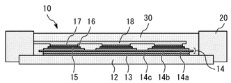
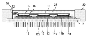
- FIG. 1 is a cross-sectional view of the semiconductor device 10 according to the first embodiment.
- the semiconductor device 10 includes a base plate 12.
- the base plate 12 is made of a metal such as Al or Cu. According to one example, the thickness of the base plate 12 is 3 mm or more.
- the insulating circuit board 14 is fixed to the central portion of the surface of the base plate 12 by the first joining material 13.
- the first joining material 13 is solder such as paste solder or plate solder.
- the joining material is one that is melted by heating and used for bonding members, and one example is solder.
- the insulating circuit board 14 has a ceramic substrate 14c, a circuit pattern 14a formed on the upper surface of the ceramic substrate 14c, and a metal layer 14b formed on the lower surface of the ceramic substrate 14c.
- the material of the ceramic substrate 14c is, for example, Al 2 O 3, Al N or Si 3 N 4 . According to one example, the thickness of the ceramic substrate 14c is 0.2 mm or more and less than 0.4 mm. According to another example, the thickness of the ceramic substrate 14c can be 0.3 mm or more and 0.35 mm or less.
- the material of the circuit pattern 14a and the metal layer 14b is, for example, Al or Cu. According to one example, the thickness of the circuit pattern 14a and the metal layer 14b can be 0.6 mm or more and less than 1.0 mm. The thicknesses of the circuit pattern 14a and the metal layer 14b may be the same or different.
- the metal layer 14b which is a component of the insulating circuit board 14, is fixed to the upper surface of the base plate 12 by the first joining material 13.
- the semiconductor element 16 is fixed to the circuit pattern 14a by the second joining material 15.
- the semiconductor element 16 has a first surface which is a lower surface and a second surface which is a surface opposite to the first surface, and the first surface is fixed to the circuit pattern 14a by the second bonding material 15.
- the semiconductor device 16 is made of, for example, Si, SiC or GaN.
- a lead frame 18 is fixed to the second surface of the semiconductor element 16 with a third joining material 17.
- the material of the lead frame 18 is, for example, Cu.
- the lead frame 18 can be bonded to a plurality of semiconductor elements 16.
- the lead frame 18 in order to fix the lead frame 18 to the three semiconductor elements 16, the lead frame 18 has a length equivalent to the width of the insulating circuit board 14.
- one lead frame can be fixed to a plurality of semiconductor elements with a third joining material.
- the lead frame 18 is supported by the case 20 by being partially embedded in the case 20 or partially attached to the case 20.
- the case 20 is fixed to the outer edge portion of the base plate 12 and surrounds a plurality of semiconductor elements 16.
- the material of the case 20 is, for example, PPS.
- the inside of the case 20 is filled with a sealing material 22.
- the encapsulant 22 is, for example, a silicone gel.
- the warp of the entire semiconductor device 10 is suppressed.
- the suppression of the warp is realized by canceling the restoring force in the upward convex warp direction in the insulating circuit board 14 and the restoring force in the downward convex warp direction in the base plate 12. That is, the insulating circuit board 14 has an upward convex shape if no force from others is applied, and the base plate 12 has a downward convex shape if no force from others is applied, but these are joined by the first bonding material 13. By doing so, the warpage of both is offset.
- the reason why the insulating circuit board 14 exhibits the restoring force in the upward convex direction is mainly due to the assembly of the semiconductor device accompanied by heating.
- the insulating circuit board 14 tends to warp in the upward convex direction with heating that melts the first joining material 13, the second joining material 15, and the third joining material 17.
- the reason why the base plate 12 exhibits the restoring force in the downward convex direction is that the base plate 12 is initially warped in the same direction.
- the warp of the assembled semiconductor device 10 is suppressed in the entire device.
- the bonding between the lead frame 18 and the semiconductor element 16 can be stabilized.
- the thickness variation of the third joining material 17 between the lead frame 18 and the semiconductor element 16 is reduced, whereby the power cycle (P / C) reliability can be improved.
- the semiconductor element 16 and the lead frame 18 are assembled in a state where the structure including the base plate 12 and the insulating circuit board 14 is almost flat. The assembly becomes easy.
- the thickness of the circuit pattern 14a and the metal layer 14b is 0.6 mm while the ceramic substrate 14c is relatively thin, 0.2 mm or more and less than 0.4 mm, or 0.3 mm or more and 0.35 mm or less.
- the coefficient of linear thermal expansion of the insulating circuit board 14 can be brought closer to the coefficient of linear thermal expansion of the circuit pattern 14a and the metal layer 14b.
- the apparent coefficient of linear expansion of the insulating circuit board 14 approaches the coefficient of linear expansion of the base plate 12, and the thermal stress applied to the first joining material 13 which is the joining layer is relaxed. As a result, cracks generated in the first joining material 13 during the temperature cycle test can be suppressed.
- the thickness of the circuit pattern 14a is 1.5 times or more the thickness of the ceramic substrate 14c, and the thickness of the metal layer 14b is also 1.5 times or more.
- the apparent linear expansion coefficient of 14 approaches the linear expansion coefficient of the circuit pattern 14a and the metal layer 14b.
- the circuit pattern 14a, the metal layer 14b, and the base plate 12 are made of the same material, the deviation of the linear expansion coefficient between the insulating circuit board 14 and the base plate 12 can be reduced. As a result, the thermal stress applied to the first joining material 13 is relaxed, and the effect of reducing the occurrence of cracks during the temperature cycle test can be enhanced.
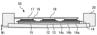
- FIG. 2 is a cross-sectional view showing an example of a semiconductor device before assembly.
- the base plate 12 is initially warped.
- the base plate 12 before assembling the semiconductor device has a downwardly convex warp.
- FIG. 2 shows that the height difference W1 is generated on the lower surface of the base plate 12 because the base plate 12 is along the downward convex direction.
- the bottom surface of the outer edge of the base plate 12 is higher than the central bottom surface of the base plate 12 by less than 1.0 mm due to the warp of the downward convex shape.
- Such a state is said to have a warp amount of less than 1.0 mm.
- this amount of warpage can be less than 0.6 mm.
- the steps for completing the configuration of FIG. 2 include the following steps. (1) Fix the outer edge portion of the base plate 12 to the case 20. (2) The insulating circuit board 14 is placed on the base plate 12 via the first joining material 13. (3) The semiconductor element 16 is placed on the circuit pattern 14a via the second joining material 15. (4) The lead frame 18 is placed on the semiconductor element 16 via the third joining material 17.
- the insulating circuit board 14 is fixed to the base plate 12, the semiconductor element 16 is fixed to the insulating circuit board 14, and the lead frame is used. 18 is fixed to the semiconductor element 16.
- the insulating circuit board 14 is fixed to the base plate 12, the semiconductor element 16 is fixed to the insulating circuit board 14, and then the lead frame 18 is fixed to the semiconductor element 16.
- the semiconductor element 16 is fixed to the insulating circuit board 14, and then the lead frame 18 is fixed to the semiconductor element 16.
- the heating for melting the bonding material generates a force that warps the insulating circuit board 14 into an upward convex shape.
- the force that causes the insulating circuit board 14 to warp in an upward convex shape is alleviated by the warping of the base plate 12.
- the warp of the insulating circuit board 14 is suppressed, and the insulating circuit board 14 has a flat shape or a shape close to it.
- the warp of the base plate 12 is also alleviated, and the base plate 12 has a flat shape or a shape close to it. In this way, the semiconductor device 10 of FIG. 1 is completed.
- the warp of the device generated in the manufacturing process and the initial warp of the base plate 12 are canceled out, and the warp at the time of assembling can be reduced.
- the warp of the configuration including the insulating circuit board 14 and the base plate 12 it is possible to improve the assembling property and reduce the thickness variation of the third bonding layer 17 to improve the P / C reliability. can.
- the modification, modification, or alternative described in the first embodiment can be applied to the semiconductor device and the method for manufacturing the semiconductor device according to the following embodiment.
- the differences between the semiconductor device and the method for manufacturing the semiconductor device according to the following embodiments will be mainly described.
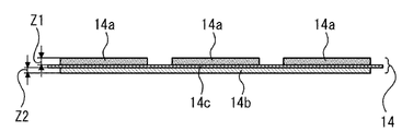
- FIG. 3 is a cross-sectional view of the insulating circuit board 14 according to the second embodiment.
- the circuit pattern 14a is thicker than the metal layer 14c.
- FIG. 3 shows that the thickness Z1 of the circuit pattern 14a is larger than the thickness Z2 of the metal layer 14c.
- the thickness of the circuit pattern 14a is 0.6 mm or more and less than 1.0 mm.
- the insulating circuit board 14 according to the second embodiment is hard to warp, the initial warp of the base plate 12 can be reduced. Further, the restoring force in the upward convex direction of the insulating circuit board 14 and the restoring force in the downward convex direction of the base plate 12 can both be set to small values.
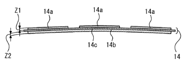
- FIG. 4 is a cross-sectional view of the insulating circuit board 14 according to the comparative example.
- the thickness of the circuit pattern 14a and the thickness of the metal layer 14c are matched. That is, the thickness Z1 and the thickness Z2 match. In this case, the insulating circuit board 14 is warped relatively large.
- FIG. 5 is a cross-sectional view of the semiconductor device according to the third embodiment.
- the inside of the case 20 is filled with the resin 30.
- the resin 30 covers all configurations enclosed by the case 20. Since the resin 30 has higher elasticity and higher adhesiveness than the gel, the use of the resin 30 alleviates the thermal stress applied to the first bonding material 13. Further, stable reliability can be obtained even if the thicknesses of the third joining material 17 and the first joining material 13 vary due to the restraint of the resin 30. Further, by restraining the resin 30, the effect of suppressing cracks in the first joining material 13 can be enhanced as compared with the first embodiment, so that the distance from the semiconductor element 16 to the end of the circuit pattern 14a can be shortened. Become. The shortening of the distance makes it possible to reduce the size of the semiconductor device.
- FIG. 6 is a cross-sectional view of the semiconductor device according to the fourth embodiment.
- This semiconductor device includes terminals 40. A part of the terminal 40 is fixed to the case 20, and another part is inside the case 20.
- the terminal 40 is fixed to the lead frame 18 by the fourth joining material 42 in the region surrounded by the case 20. In the example of FIG. 6, the upper surface of the terminal 40 and the lower surface of the lead frame 18 are fixed by the fourth joining material 42.
- the vertical position of the lead frame 18 can be changed. For example, by changing the thickness of the fourth joining material 42 or changing the shape of the lead frame 18, the position of the lead frame 18 directly above the semiconductor element 16 can be easily changed.
- the lead frame 18 By making it possible to change the position of the lead frame 18 in this way, when the position of the semiconductor element 16 varies due to the warp of the semiconductor device, the lead frame 18 can be provided at a position that follows the variation. can. Therefore, the work of fixing the lead frame 18 to the semiconductor element 16 can be performed reliably and easily.
- FIG. 7 is a cross-sectional view of the semiconductor device according to the fifth embodiment.
- the base plate 12 has pin fins 12a on the back surface side thereof.
- the semiconductor device of FIG. 7 is provided with a base plate 12 provided with pin fins 12a, which is a cooling device, on the back surface of the semiconductor device without interposing thermal grease or the like.
- Such a structure is called a direct cooling structure.
- the direct cooling structure the temperature distribution of the vertical structure appears remarkably during the power cycle test. When the temperature distribution of the vertical structure is large, the stress generated in the first joining material 13 also becomes large. Therefore, it is extremely important to suppress cracks in the first joining material 13.
- the suppression of the warp of the semiconductor device by offsetting the restoring force contributes to the suppression of cracks in the first joining material 13. Therefore, the thermal performance of the semiconductor device provided with the pin fins is improved, and the reliability can be improved and the device can be miniaturized.
- the effect may be enhanced by combining the features of the semiconductor device according to each of the above embodiments.
Landscapes
- Cooling Or The Like Of Semiconductors Or Solid State Devices (AREA)
- Chemical & Material Sciences (AREA)
- Engineering & Computer Science (AREA)
- Ceramic Engineering (AREA)
- Structures Or Materials For Encapsulating Or Coating Semiconductor Devices Or Solid State Devices (AREA)
Abstract
Description
図1は、実施の形態1に係る半導体装置10の断面図である。半導体装置10は、ベース板12を備えている。ベース板12は例えばAl又はCuなどの金属で形成されている。一例によれば、ベース板12の厚さは3mm以上である。
(1)ベース板12の外縁部分をケース20に固定すること。
(2)絶縁回路基板14を、第1接合材13を介してベース板12の上にのせること。
(3)回路パターン14aの上に第2接合材15を介して半導体素子16をのせること。
(4)半導体素子16の上に第3接合材17を介してリードフレーム18をのせること。
図3は、実施の形態2に係る絶縁回路基板14の断面図である。回路パターン14aは金属層14cより厚い。図3には、回路パターン14aの厚さZ1が、金属層14cの厚さZ2より大きいことが示されている。一例によれば、回路パターン14aの厚さは0.6mm以上1.0mm未満である。回路パターン14aを金属層14cより厚くすることで、高温時における絶縁回路基板14の反りが抑制される。したがって、第3接合層17の厚みばらつきをさらに低減させてP/C信頼性を向上させることができる。
図5は、実施の形態3に係る半導体装置の断面図である。ケース20の内部には樹脂30が充填されている。一例によれば、樹脂30は、ケース20によって囲まれたすべての構成を覆う。樹脂30は、ゲルに比べて高弾性かつ高粘着なため、樹脂30を採用することで、第1接合材13に加わる熱応力が緩和される。また、樹脂30の拘束により第3接合材17と第1接合材13の厚みにばらつきが生じても安定した信頼性を得ることができる。さらに、樹脂30の拘束により、実施の形態1よりも第1接合材13の亀裂を抑制する効果を高めることができるので、半導体素子16から回路パターン14a端部までの距離を縮めることが可能になる。当該距離の短縮は、半導体装置の小型化を可能とする。
図6は、実施の形態4に係る半導体装置の断面図である。この半導体装置は端子40を備えている。端子40は、一部がケース20に固定され、別の部分がケース20の内部にあるものである。端子40は、ケース20に囲まれた領域において、第4接合材42でリードフレーム18に固定されている。図6の例では、端子40の上面と、リードフレーム18の下面が第4接合材42で固定されている。
図7は、実施の形態5に係る半導体装置の断面図である。ベース板12は、その裏面側にピンフィン12aを有している。図7の半導体装置は、サーマルグリースなどを介在させずに、半導体装置裏面に冷却装置であるピンフィン12aを備えたベース板12を設けたものである。このような構造は、直接冷却構造と呼ばれる。直接冷却構造では、パワーサイクル試験時において、縦方向構造の温度分布が顕著に現れる。縦方向構造の温度分布が大きいと、第1接合材13に発生する応力も大きくなる。そこで、第1接合材13の亀裂を抑制することが極めて重要となる。
Claims (10)
- ベース板と、
セラミック基板と、前記セラミック基板の上面に形成された回路パターンと、前記セラミック基板の下面に形成された金属層と、を有し、前記金属層は、第1接合材で前記ベース板の上面に固定された、絶縁回路基板と、
第1面と、前記第1面と反対の面である第2面を有し、前記第1面は、第2接合材で前記回路パターンに固定された、半導体素子と、
前記第2面に第3接合材で固定されたリードフレームと、
前記ベース板の外縁部分に固定されて前記半導体素子を囲むケースと、を備え、
前記絶縁回路基板には上に凸に反る方向に復元力が働き、前記ベース板には下に凸に反る方向に復元力が働くことを特徴とする半導体装置。 - 前記半導体素子は複数提供され、1つの前記リードフレームが前記第3接合材で複数の前記半導体素子に固定されたことを特徴とする請求項1に記載の半導体装置。
- 前記回路パターンは、前記金属層より厚いことを特徴とする請求項1又は2に記載の半導体装置。
- 前記ケースの内部に充填された樹脂を備えたことを特徴とする請求項1から3のいずれか1項に記載の半導体装置。
- 前記ケースに固定され、前記ケースに囲まれた領域において第4接合材で前記リードフレームに固定された端子を備えた請求項1から4のいずれか1項に記載の半導体装置。
- 前記ベース板は、ピンフィンを有することを特徴とする請求項1から5のいずれか1項に記載の半導体装置。
- 前記回路パターンの厚さは、前記セラミック基板の厚さの1.5倍以上であり、
前記金属層の厚さは、前記セラミック基板の厚さの1.5倍以上であることを特徴とする請求項1から6のいずれか1項に記載の半導体装置。 - 前記回路パターンと、前記金属層と、前記ベース板は同じ材料であることを特徴とする請求項1から7のいずれか1項に記載の半導体装置。
- 下凸形状の反りを有するベース板の外縁部分をケースに固定することと、
セラミック基板と、前記セラミック基板の上面に形成された回路パターンと、前記セラミック基板の下面に形成された金属層と、を有する絶縁回路基板を、第1接合材を介して前記ベース板の上にのせることと、
前記回路パターンの上に、第2接合材を介して半導体素子をのせることと、
前記半導体素子の上に、第3接合材を介してリードフレームをのせることと、
前記第1接合材と、前記第2接合材と、前記第3接合材を溶融させることと、
前記溶融によって生じた前記絶縁回路基板を上凸形状に反らせる力が、前記ベース板の反りによって緩和されることで前記絶縁回路基板の反りが抑制されることと、を備えた半導体装置の製造方法。 - 前記下凸形状の反りによって、前記ベース板の外縁底面は、前記ベース板の中央底面より、1.0mm未満だけ高いことを特徴とする請求項9に記載の半導体装置の製造方法。
Priority Applications (5)
| Application Number | Priority Date | Filing Date | Title |
|---|---|---|---|
| PCT/JP2020/039959 WO2022085192A1 (ja) | 2020-10-23 | 2020-10-23 | 半導体装置、半導体装置の製造方法 |
| JP2022556359A JP7359317B2 (ja) | 2020-10-23 | 2020-10-23 | 半導体装置、半導体装置の製造方法 |
| CN202080106361.8A CN116368612A (zh) | 2020-10-23 | 2020-10-23 | 半导体装置、半导体装置的制造方法 |
| DE112020007724.1T DE112020007724T5 (de) | 2020-10-23 | 2020-10-23 | Halbleitervorrichtung und Verfahren zur Fertigung der Halbleitervorrichtung |
| US17/996,888 US12575445B2 (en) | 2020-10-23 | 2020-10-23 | Semiconductor apparatus and method for manufacturing semiconductor apparatus |
Applications Claiming Priority (1)
| Application Number | Priority Date | Filing Date | Title |
|---|---|---|---|
| PCT/JP2020/039959 WO2022085192A1 (ja) | 2020-10-23 | 2020-10-23 | 半導体装置、半導体装置の製造方法 |
Publications (1)
| Publication Number | Publication Date |
|---|---|
| WO2022085192A1 true WO2022085192A1 (ja) | 2022-04-28 |
Family
ID=81290324
Family Applications (1)
| Application Number | Title | Priority Date | Filing Date |
|---|---|---|---|
| PCT/JP2020/039959 Ceased WO2022085192A1 (ja) | 2020-10-23 | 2020-10-23 | 半導体装置、半導体装置の製造方法 |
Country Status (5)
| Country | Link |
|---|---|
| US (1) | US12575445B2 (ja) |
| JP (1) | JP7359317B2 (ja) |
| CN (1) | CN116368612A (ja) |
| DE (1) | DE112020007724T5 (ja) |
| WO (1) | WO2022085192A1 (ja) |
Citations (7)
| Publication number | Priority date | Publication date | Assignee | Title |
|---|---|---|---|---|
| JPH0982844A (ja) * | 1995-09-20 | 1997-03-28 | Mitsubishi Electric Corp | 半導体モジュール基板及びその製造方法 |
| JPH10340975A (ja) * | 1997-06-09 | 1998-12-22 | Hitachi Ltd | パワー半導体モジュール |
| JP2002084046A (ja) * | 2000-09-07 | 2002-03-22 | Toshiba Corp | セラミックス回路基板 |
| JP2008091959A (ja) * | 2007-12-28 | 2008-04-17 | Fuji Electric Device Technology Co Ltd | 半導体装置の製造方法 |
| WO2012108073A1 (ja) * | 2011-02-08 | 2012-08-16 | 富士電機株式会社 | 半導体モジュール用放熱板の製造方法、その放熱板およびその放熱板を用いた半導体モジュール |
| JP2015130430A (ja) * | 2014-01-08 | 2015-07-16 | 三菱マテリアル株式会社 | ヒートシンク付パワーモジュール用基板及びその製造方法 |
| US20190273034A1 (en) * | 2018-03-05 | 2019-09-05 | Delta Electronics (Shanghai) Co., Ltd. | Power module and production method of the same |
Family Cites Families (11)
| Publication number | Priority date | Publication date | Assignee | Title |
|---|---|---|---|---|
| JP4656126B2 (ja) | 2002-08-13 | 2011-03-23 | 富士電機システムズ株式会社 | 半導体装置 |
| US6844621B2 (en) * | 2002-08-13 | 2005-01-18 | Fuji Electric Co., Ltd. | Semiconductor device and method of relaxing thermal stress |
| JP4207896B2 (ja) | 2005-01-19 | 2009-01-14 | 富士電機デバイステクノロジー株式会社 | 半導体装置 |
| WO2008142760A1 (ja) * | 2007-05-18 | 2008-11-27 | Sansha Electric Manufacturing Co., Ltd. | 電力用半導体モジュール |
| JP5241344B2 (ja) | 2008-06-30 | 2013-07-17 | 日立オートモティブシステムズ株式会社 | パワーモジュール及び電力変換装置 |
| JP6480098B2 (ja) * | 2013-10-31 | 2019-03-06 | 三菱電機株式会社 | 半導体装置 |
| JP2015170785A (ja) | 2014-03-10 | 2015-09-28 | 三菱電機株式会社 | 絶縁基板および電力用半導体装置 |
| JP6341822B2 (ja) * | 2014-09-26 | 2018-06-13 | 三菱電機株式会社 | 半導体装置 |
| DE112014007285B4 (de) | 2014-12-26 | 2024-01-18 | Mitsubishi Electric Corporation | Halbleitermodul |
| DE112016000655B4 (de) * | 2015-09-17 | 2023-12-07 | Fuji Electric Co., Ltd. | Verfahren zum herstellen einer halbleitervorrichtung |
| JP2019207897A (ja) | 2016-09-29 | 2019-12-05 | 三菱電機株式会社 | パワーモジュール、その製造方法および電力変換装置 |
-
2020
- 2020-10-23 DE DE112020007724.1T patent/DE112020007724T5/de active Pending
- 2020-10-23 US US17/996,888 patent/US12575445B2/en active Active
- 2020-10-23 WO PCT/JP2020/039959 patent/WO2022085192A1/ja not_active Ceased
- 2020-10-23 CN CN202080106361.8A patent/CN116368612A/zh active Pending
- 2020-10-23 JP JP2022556359A patent/JP7359317B2/ja active Active
Patent Citations (7)
| Publication number | Priority date | Publication date | Assignee | Title |
|---|---|---|---|---|
| JPH0982844A (ja) * | 1995-09-20 | 1997-03-28 | Mitsubishi Electric Corp | 半導体モジュール基板及びその製造方法 |
| JPH10340975A (ja) * | 1997-06-09 | 1998-12-22 | Hitachi Ltd | パワー半導体モジュール |
| JP2002084046A (ja) * | 2000-09-07 | 2002-03-22 | Toshiba Corp | セラミックス回路基板 |
| JP2008091959A (ja) * | 2007-12-28 | 2008-04-17 | Fuji Electric Device Technology Co Ltd | 半導体装置の製造方法 |
| WO2012108073A1 (ja) * | 2011-02-08 | 2012-08-16 | 富士電機株式会社 | 半導体モジュール用放熱板の製造方法、その放熱板およびその放熱板を用いた半導体モジュール |
| JP2015130430A (ja) * | 2014-01-08 | 2015-07-16 | 三菱マテリアル株式会社 | ヒートシンク付パワーモジュール用基板及びその製造方法 |
| US20190273034A1 (en) * | 2018-03-05 | 2019-09-05 | Delta Electronics (Shanghai) Co., Ltd. | Power module and production method of the same |
Also Published As
| Publication number | Publication date |
|---|---|
| JPWO2022085192A1 (ja) | 2022-04-28 |
| JP7359317B2 (ja) | 2023-10-11 |
| DE112020007724T5 (de) | 2023-08-10 |
| US20230154808A1 (en) | 2023-05-18 |
| CN116368612A (zh) | 2023-06-30 |
| US12575445B2 (en) | 2026-03-10 |
Similar Documents
| Publication | Publication Date | Title |
|---|---|---|
| KR102864411B1 (ko) | 반도체 장치 | |
| EP3226292B1 (en) | Lead frame, semiconductor device, method for manufacturing lead frame, and method for manufacturing semiconductor device | |
| JP5665729B2 (ja) | 電力用半導体装置 | |
| KR102231769B1 (ko) | 고열전도를 위한 히트싱크 노출형 반도체 패키지 및 그 제조방법 | |
| KR100562060B1 (ko) | 수지밀봉형 반도체장치 | |
| KR20130045797A (ko) | 부재의 접합 구조체, 부재의 접합 방법, 및 패키지 | |
| JP6043049B2 (ja) | 半導体装置の実装構造及び半導体装置の実装方法 | |
| WO2022085192A1 (ja) | 半導体装置、半導体装置の製造方法 | |
| JP7229384B2 (ja) | 半導体装置および半導体装置の製造方法 | |
| KR102371636B1 (ko) | 양면 기판 반도체 제조 방법 | |
| JP6011410B2 (ja) | 半導体装置用接合体、パワーモジュール用基板及びパワーモジュール | |
| JP2014143342A (ja) | 半導体モジュール及びその製造方法 | |
| JP7329919B2 (ja) | 半導体装置、半導体装置の製造方法及びクリップリード | |
| JP4861200B2 (ja) | パワーモジュール | |
| TWI690954B (zh) | 電子模組、引線框以及電子模組的製造方法 | |
| JPH09129823A (ja) | 半導体装置 | |
| WO2017077729A1 (ja) | 半導体モジュール及びその製造方法 | |
| KR20250118258A (ko) | 양면 방열 반도체 패키지 및 이의 제조방법 | |
| JP3858857B2 (ja) | 半導体装置 | |
| JP2011108892A (ja) | パッケージ構造 | |
| US20050269689A1 (en) | Conductor device and method of manufacturing thereof | |
| CN117957649A (zh) | 半导体装置及半导体装置的制造方法 | |
| WO2025027845A1 (ja) | 半導体装置および半導体装置の製造方法 | |
| CN114914217A (zh) | 半导体装置及半导体装置的制造方法 | |
| JPH08288441A (ja) | 電力半導体装置 |
Legal Events
| Date | Code | Title | Description |
|---|---|---|---|
| 121 | Ep: the epo has been informed by wipo that ep was designated in this application |
Ref document number: 20958740 Country of ref document: EP Kind code of ref document: A1 |
|
| ENP | Entry into the national phase |
Ref document number: 2022556359 Country of ref document: JP Kind code of ref document: A |
|
| 122 | Ep: pct application non-entry in european phase |
Ref document number: 20958740 Country of ref document: EP Kind code of ref document: A1 |
|
| WWG | Wipo information: grant in national office |
Ref document number: 17996888 Country of ref document: US |