WO2022079995A1 - 窒化物半導体装置 - Google Patents
窒化物半導体装置 Download PDFInfo
- Publication number
- WO2022079995A1 WO2022079995A1 PCT/JP2021/029951 JP2021029951W WO2022079995A1 WO 2022079995 A1 WO2022079995 A1 WO 2022079995A1 JP 2021029951 W JP2021029951 W JP 2021029951W WO 2022079995 A1 WO2022079995 A1 WO 2022079995A1
- Authority
- WO
- WIPO (PCT)
- Prior art keywords
- gate electrode
- gate
- source
- electrode
- lead
- Prior art date
- Legal status (The legal status is an assumption and is not a legal conclusion. Google has not performed a legal analysis and makes no representation as to the accuracy of the status listed.)
- Ceased
Links
Images








Classifications
-
- H—ELECTRICITY
- H10—SEMICONDUCTOR DEVICES; ELECTRIC SOLID-STATE DEVICES NOT OTHERWISE PROVIDED FOR
- H10D—INORGANIC ELECTRIC SEMICONDUCTOR DEVICES
- H10D30/00—Field-effect transistors [FET]
- H10D30/40—FETs having zero-dimensional [0D], one-dimensional [1D] or two-dimensional [2D] charge carrier gas channels
- H10D30/47—FETs having zero-dimensional [0D], one-dimensional [1D] or two-dimensional [2D] charge carrier gas channels having two-dimensional [2D] charge carrier gas channels, e.g. nanoribbon FETs or high electron mobility transistors [HEMT]
- H10D30/471—High electron mobility transistors [HEMT] or high hole mobility transistors [HHMT]
- H10D30/475—High electron mobility transistors [HEMT] or high hole mobility transistors [HHMT] having wider bandgap layer formed on top of lower bandgap active layer, e.g. undoped barrier HEMTs such as i-AlGaN/GaN HEMTs
-
- H—ELECTRICITY
- H10—SEMICONDUCTOR DEVICES; ELECTRIC SOLID-STATE DEVICES NOT OTHERWISE PROVIDED FOR
- H10D—INORGANIC ELECTRIC SEMICONDUCTOR DEVICES
- H10D64/00—Electrodes of devices having potential barriers
- H10D64/20—Electrodes characterised by their shapes, relative sizes or dispositions
- H10D64/23—Electrodes carrying the current to be rectified, amplified, oscillated or switched, e.g. sources, drains, anodes or cathodes
-
- H—ELECTRICITY
- H10—SEMICONDUCTOR DEVICES; ELECTRIC SOLID-STATE DEVICES NOT OTHERWISE PROVIDED FOR
- H10D—INORGANIC ELECTRIC SEMICONDUCTOR DEVICES
- H10D64/00—Electrodes of devices having potential barriers
- H10D64/20—Electrodes characterised by their shapes, relative sizes or dispositions
- H10D64/23—Electrodes carrying the current to be rectified, amplified, oscillated or switched, e.g. sources, drains, anodes or cathodes
- H10D64/251—Source or drain electrodes for field-effect devices
- H10D64/258—Source or drain electrodes for field-effect devices characterised by the relative positions of the source or drain electrodes with respect to the gate electrode
-
- H—ELECTRICITY
- H10—SEMICONDUCTOR DEVICES; ELECTRIC SOLID-STATE DEVICES NOT OTHERWISE PROVIDED FOR
- H10D—INORGANIC ELECTRIC SEMICONDUCTOR DEVICES
- H10D64/00—Electrodes of devices having potential barriers
- H10D64/20—Electrodes characterised by their shapes, relative sizes or dispositions
- H10D64/27—Electrodes not carrying the current to be rectified, amplified, oscillated or switched, e.g. gates
- H10D64/311—Gate electrodes for field-effect devices
- H10D64/411—Gate electrodes for field-effect devices for FETs
-
- H—ELECTRICITY
- H10—SEMICONDUCTOR DEVICES; ELECTRIC SOLID-STATE DEVICES NOT OTHERWISE PROVIDED FOR
- H10D—INORGANIC ELECTRIC SEMICONDUCTOR DEVICES
- H10D8/00—Diodes
- H10D8/20—Breakdown diodes, e.g. avalanche diodes
- H10D8/25—Zener diodes
-
- H—ELECTRICITY
- H10—SEMICONDUCTOR DEVICES; ELECTRIC SOLID-STATE DEVICES NOT OTHERWISE PROVIDED FOR
- H10D—INORGANIC ELECTRIC SEMICONDUCTOR DEVICES
- H10D8/00—Diodes
- H10D8/422—PN diodes having the PN junctions in mesas
-
- H—ELECTRICITY
- H10—SEMICONDUCTOR DEVICES; ELECTRIC SOLID-STATE DEVICES NOT OTHERWISE PROVIDED FOR
- H10W—GENERIC PACKAGES, INTERCONNECTIONS, CONNECTORS OR OTHER CONSTRUCTIONAL DETAILS OF DEVICES COVERED BY CLASS H10
- H10W20/00—Interconnections in chips, wafers or substrates
- H10W20/20—Interconnections within wafers or substrates, e.g. through-silicon vias [TSV]
-
- H—ELECTRICITY
- H10—SEMICONDUCTOR DEVICES; ELECTRIC SOLID-STATE DEVICES NOT OTHERWISE PROVIDED FOR
- H10D—INORGANIC ELECTRIC SEMICONDUCTOR DEVICES
- H10D62/00—Semiconductor bodies, or regions thereof, of devices having potential barriers
- H10D62/10—Shapes, relative sizes or dispositions of the regions of the semiconductor bodies; Shapes of the semiconductor bodies
- H10D62/17—Semiconductor regions connected to electrodes not carrying current to be rectified, amplified or switched, e.g. channel regions
- H10D62/343—Gate regions of field-effect devices having PN junction gates
-
- H—ELECTRICITY
- H10—SEMICONDUCTOR DEVICES; ELECTRIC SOLID-STATE DEVICES NOT OTHERWISE PROVIDED FOR
- H10D—INORGANIC ELECTRIC SEMICONDUCTOR DEVICES
- H10D62/00—Semiconductor bodies, or regions thereof, of devices having potential barriers
- H10D62/80—Semiconductor bodies, or regions thereof, of devices having potential barriers characterised by the materials
- H10D62/85—Semiconductor bodies, or regions thereof, of devices having potential barriers characterised by the materials being Group III-V materials, e.g. GaAs
- H10D62/8503—Nitride Group III-V materials, e.g. AlN or GaN
-
- H—ELECTRICITY
- H10—SEMICONDUCTOR DEVICES; ELECTRIC SOLID-STATE DEVICES NOT OTHERWISE PROVIDED FOR
- H10D—INORGANIC ELECTRIC SEMICONDUCTOR DEVICES
- H10D64/00—Electrodes of devices having potential barriers
- H10D64/111—Field plates
-
- H—ELECTRICITY
- H10—SEMICONDUCTOR DEVICES; ELECTRIC SOLID-STATE DEVICES NOT OTHERWISE PROVIDED FOR
- H10D—INORGANIC ELECTRIC SEMICONDUCTOR DEVICES
- H10D64/00—Electrodes of devices having potential barriers
- H10D64/20—Electrodes characterised by their shapes, relative sizes or dispositions
- H10D64/23—Electrodes carrying the current to be rectified, amplified, oscillated or switched, e.g. sources, drains, anodes or cathodes
- H10D64/251—Source or drain electrodes for field-effect devices
- H10D64/257—Source or drain electrodes for field-effect devices for lateral devices wherein the source or drain electrodes are characterised by top-view geometrical layouts, e.g. interdigitated, semi-circular, annular or L-shaped electrodes
-
- H—ELECTRICITY
- H10—SEMICONDUCTOR DEVICES; ELECTRIC SOLID-STATE DEVICES NOT OTHERWISE PROVIDED FOR
- H10D—INORGANIC ELECTRIC SEMICONDUCTOR DEVICES
- H10D64/00—Electrodes of devices having potential barriers
- H10D64/20—Electrodes characterised by their shapes, relative sizes or dispositions
- H10D64/27—Electrodes not carrying the current to be rectified, amplified, oscillated or switched, e.g. gates
Definitions
- the present disclosure relates to a nitride semiconductor device using a nitride semiconductor such as gallium nitride (GaN) as a semiconductor material.
- a nitride semiconductor such as gallium nitride (GaN) as a semiconductor material.
- GaN-FETs field effect transistors
- GaN which is a nitride semiconductor
- a GaN-FET a GaN layer is formed as a channel layer and AlGaN is formed as a barrier layer on a semiconductor substrate, and a two-dimensional electron gas generated by spontaneous polarization and piezopolarization at a heterojunction interface formed by these two layers. Is generally used as a channel.
- a channel current flows in a direction parallel to the substrate.
- the source pad, drain pad, and gate pad that supply voltage or pass current from the outside through wire bonding or the like to the FET are all formed on the surface side of the substrate. Therefore, in order to reduce the cost of the GaN-FET by reducing the chip area, it is important to reduce the pad area occupying the entire chip area.
- the wiring of the gate electrode is formed in the element separation region outside the active region.
- the gate electrode 8 is bundled outside the active region and further bypassed the outer periphery of the active region and connected to the gate electrode pad layer 23.” be.
- the present disclosure shows that by wiring the gate electrode on the active region, the wiring length to the gate electrode pad is shortened, and as a result, the wiring resistance of the gate is reduced, and the nitride suitable for high-speed switching operation is used.
- the main purpose is to provide semiconductor devices.
- a substrate a semiconductor laminated structure composed of a plurality of nitride semiconductor layers on the substrate, and an upper surface side of the semiconductor laminated structure.
- a first active region surrounded by an element separation region, a source electrode on the first active region, and a first located on both sides separated from the source electrode in the first direction in a plan view.
- the gate electrode 1, the second gate electrode, and the drain electrode have a finger-shaped portion extending in a second direction perpendicular to the first direction in a plan view, and a second gate electrode is placed on the source electrode.
- the dielectric film of 1 is formed, and the first gate electrode and the second gate electrode are electrically connected by a gate electrode connecting portion formed on the first dielectric film. ing.
- a substrate, a semiconductor laminated structure composed of a plurality of nitride semiconductor layers on the substrate, and the semiconductor laminate are used.
- a first active region surrounded by an element separation region, a first source electrode on the first active region, and a plan view of the first source electrode.
- the first gate electrode, the second gate electrode, the second source electrode, and the second source electrode located on both sides separated from each other in the first direction are separated from each other in the first direction in a plan view.
- the gate electrode, the fourth gate electrode has a finger-shaped portion extending in a second direction perpendicular to the first direction in a plan view, and is above the first source electrode and the second source electrode.
- a first dielectric film is formed in the semiconductor, and the first gate electrode and the second gate electrode are formed by a first gate electrode connecting portion formed on the first dielectric film. It is electrically connected, and the third gate electrode and the fourth gate electrode are electrically connected by a second gate electrode connecting portion formed on the first dielectric film.
- the present disclosure provides a nitride semiconductor device capable of reducing gate wiring resistance.
- FIG. 1 is a plan view of the nitride semiconductor device according to the first embodiment.
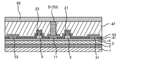
- FIG. 2A is a cross-sectional view taken along the line IIa-IIa of the nitride semiconductor device of FIG. 1 in the first embodiment.
- FIG. 2B is a cross-sectional view taken along the line IIb-IIb of the nitride semiconductor device of FIG. 1 in the first embodiment.
- FIG. 2C is a cross-sectional view taken along the line IIc-IIc of the nitride semiconductor device of FIG. 1 in the first embodiment.
- FIG. 3 is a cross-sectional view of the nitride semiconductor device according to the first modification of the first embodiment.
- FIG. 4 is a plan view of the nitride semiconductor device according to the second modification of the first embodiment.
- FIG. 5A is a cross-sectional view taken along the line Va—Va of the nitride semiconductor device of FIG. 4 in the second modification of the first embodiment.
- FIG. 5B is a cross-sectional view taken along the line Vb-Vb of the nitride semiconductor device of FIG. 4 in the second modification of the first embodiment.
- FIG. 5C is a cross-sectional view taken along the line Vc—Vc of the nitride semiconductor device of FIG. 4 in the second modification of the first embodiment.
- FIG. 6 is a plan view of the nitride semiconductor device according to the second embodiment.
- FIG. 7 is a plan view of the nitride semiconductor device in the modified example of the second embodiment.
- FIG. 8 is a cross-sectional view of a PN diode used in the nitride semiconductor device in the modified example of the second embodiment.
- FIG. 9 is a plan view of the nitride semiconductor device in the third embodiment.
- FIG. 10 is an enlarged plan view of the dotted line portion M in FIG. 9.
- FIG. 11 is an enlarged plan view of the dotted line portion N of FIG.
- FIG. 12 is a plan view of the nitride semiconductor device according to the fourth embodiment.
- FIG. 13A is a cross-sectional view taken along the line XIIIa-XIIIa of the nitride semiconductor device of FIG. 12 in the fourth embodiment.
- FIG. 13A is a cross-sectional view taken along the line XIIIa-XIIIa of the nitride semiconductor device of FIG. 12 in the fourth embodiment.
- FIG. 13B is a cross-sectional view taken along the line XIIIb-XIIIb of the nitride semiconductor device of FIG. 12 in the fourth embodiment.
- FIG. 13C is a cross-sectional view taken along the line XIIIc-XIIIc of the nitride semiconductor device of FIG. 12 in the fourth embodiment.
- FIG. 13D is a cross-sectional view taken along the line XIIId-XIIId of the nitride semiconductor device according to FIG. 12 in the fourth embodiment.
- FIG. 1 shows a plan view of the nitride semiconductor device 10 of the first embodiment
- FIGS. 2A, 2B, and 2C show cross-sectional views of the lines IIa-IIa, IIb-IIb, and IIc-IIc in FIG. ..
- a buffer layer 2 composed of an AlN layer and an AlGaN layer, a GaN channel layer 3, and an AlGaN barrier layer 4 are formed as a semiconductor laminate structure by epitaxial growth on a Si substrate 1. There is. On the AlGaN barrier layer 4, a p-type GaN layer 5 and a p-type GaN layer 6 that have been epitaxially grown on the AlGaN barrier layer 4 and then etched are formed. At the interface between the GaN channel layer 3 and the AlGaN barrier layer 4, a high-concentration two-dimensional electron gas is formed due to the effects of piezoelectric polarization and spontaneous polarization.
- the region in which the two-dimensional electron gas is formed is the first active region 8 shown in FIG. 1, and the region in which the resistance of the two-dimensional electron gas is increased by ion implantation is the device separation region 9.
- the boundary between the first active region 8 and the device separation region 9 is the boundary 8A of the ion implantation region.
- the element separation region 9 may be formed by removing the region containing the two-dimensional electron gas by mesa etching.
- a SiN film 41 is formed as a surface protective film on the surfaces of the AlGaN barrier layer 4, the p-type GaN layer 5, and the p-type GaN layer 6, and the SiN film 41 is opened.
- the source electrode 11, the drain electrode 31, and the drain electrode 33 are formed.
- a SiO film is formed on the SiN film 41 as the first dielectric film 43.
- the first gate electrode 21 and the second gate electrode 23 are formed by opening the SiN film 41 and the first dielectric film 43 on the p-type GaN layer 5 and the p-type GaN layer 6, respectively. ..
- the first gate electrode 21 and the second gate electrode 23 are formed at positions on both sides separated from the finger-shaped source electrode 11 in the first direction in a plan view.
- the first direction is the X direction in FIG.
- the finger-shaped drain electrode 31 is located in the direction opposite to the source electrode 11 with respect to the first gate electrode 21, and the finger-shaped drain electrode 33 and the source electrode 11 with respect to the second gate electrode 23.
- the first gate electrode 21 and the second gate electrode 23, together with the p-type GaN layer 5 and the p-type GaN layer 6 at the lower portions thereof, are in the second direction perpendicular to the first direction in a plan view. It is extended in a finger shape and connected in an arc shape at both ends.
- the second direction is the Y direction in FIG.
- the leakage current flowing between the source electrode 11, the drain electrode 31, and the drain electrode 33 in the off state is reduced.
- the finger-shaped gate electrode needs to exceed the boundary 8A of the ion implantation region and reach the element separation region 9. ..
- the first gate electrode 21 and the second gate electrode 23 are each coupled by a gate electrode connecting portion 25 at the central portion thereof.
- the gate electrode connecting portion 25 is formed of the same metal layer as the first gate electrode 21 and the second gate electrode 23 at the same time. Therefore, the number of manufacturing processes does not increase.
- the gate electrode connecting portion 25 is the first dielectric film 43. It is formed on the SiO film, which is electrically insulated from the source electrode 11.
- the width of the gate electrode connecting portion 25 (in the depth direction of the paper surface) is about 3 ⁇ m, and both are designed to be larger than the first gate electrode 21 and the second gate electrode 23 having a length of about 1 ⁇ m. This design enables a back end of line using vias and plugs, which is difficult on gate electrodes.
- a first gate electrode 21, a second gate electrode 23, a gate electrode connecting portion 25, a source electrode 11, a drain electrode 31 and a drain electrode 33 are placed on the first gate electrode 21 and the drain electrode 33.
- the SiO film which is the dielectric film 47 of 2 is formed.
- the second dielectric film 47 is designed to have a thickness that prevents dielectric breakdown between the source and drain in the high withstand voltage transistor. For example, in a 600V withstand voltage transistor, when the second dielectric film 47 is a SiO film, the thickness thereof is set to 2 ⁇ m to 3 ⁇ m.
- the widths of the source electrode 11, the gate electrode connecting portion 25, and the drain electrode 31 are all about 3 ⁇ m, the ordinary photo lithography technology and the second dielectric film 47 and the first dielectric film 43 are dried.
- a via 51 on the source electrode 11, a via 61 on the gate electrode connecting portion 25, and a via 71 on the drain electrode 31 and the drain electrode 33 are formed.
- plugs 53, 63, 73 for filling the respective vias are formed.
- W tungsten
- the plug 53 is connected to the first source lead wire 55
- the plug 63 is connected to the first gate lead wire 65
- the plug 73 is connected to the first drain lead wire 75.
- the first gate electrode 21 and the second gate electrode 23 are connected by a gate electrode connecting portion 25 at the central portion. Then, a via 61 is formed in the gate electrode connecting portion 25 to perform gate wiring. Therefore, the gate wiring resistance is significantly reduced as compared with the case where the gate wiring is performed from the end of the gate electrode.
- the nitride semiconductor device 10 is suitable for high-speed switching operation due to the decrease in gate wiring resistance.
- the gate wiring is formed not on the element separation region 9 but on the first active region 8. As a result, the chip area does not increase. Further, a capacitance is generated by the first dielectric film 43 between the source electrode 11 and the gate electrode connecting portion 25. This capacitance is the capacitance between the gate and source, but in order to prevent erroneous arcs in the power transistor for switching, it is desirable to increase the capacitance between the gate and source with respect to the capacitance between the gate and drain. Therefore, by using this embodiment, it is possible to realize a power transistor for switching, which has a large gate-source capacitance and can prevent an erroneous arc.
- W is used as the plug for filling the via in the nitride semiconductor device 10 in the present embodiment
- Al aluminum
- Cu copper
- the plug and the wiring connected to the plug may be formed at the same time by using the dual damascene method.
- the number of vias 61 on the gate electrode connecting portion 25 is one in FIG. 1, a plurality of vias 61 may be formed if possible from the viewpoint of manufacturing technology. Further, the number of vias 71 on the source electrodes 11 and the drain electrodes 31 and 33 should be large in order to reduce the wiring resistance, but it is appropriately designed from the viewpoint of the manufacturing technique for forming the vias and the plugs.
- the nitride semiconductor device has a substrate, a semiconductor laminated structure composed of a plurality of nitride semiconductor layers on the substrate, and an element separation region around the upper surface side of the semiconductor laminated structure.
- a first active region surrounded by, a source electrode on the first active region, a first gate electrode and a second gate electrode located on both sides separated from the source electrode in the first direction in a plan view. It has at least one drain electrode located in the direction opposite to the source electrode with respect to the gate electrode, the first gate electrode or the second gate electrode, and the source electrode, the first gate electrode, and the first gate electrode.
- the gate electrode 2 and the drain electrode have a finger-shaped portion extending in a second direction perpendicular to the first direction in a plan view, and a first dielectric film is formed on the source electrode.
- the first gate electrode and the second gate electrode are electrically connected by a gate electrode connecting portion formed on the first dielectric film.
- the wiring of the gate electrode (this wiring includes the finger-shaped portion) is formed inside the first active region instead of the outside in a plan view, thereby shortening the wiring length and wiring the gate.
- the resistance can be reduced.
- by forming the wiring of the gate electrode inside the active region in a plan view there is an effect that the area of the chip as a nitride semiconductor device can be reduced.
- the first gate electrode, the second gate electrode, and the gate electrode connecting portion may be formed of the same metal layer.
- the wiring resistance of the gate electrode can be reduced by the gate electrode connecting portion. Moreover, there is an effect that the manufacturing process is not increased in the formation of the first gate electrode, the second gate electrode and the gate electrode connecting portion.
- the width of the gate electrode connecting portion may be larger than the first gate electrode length and the second gate electrode length.
- FIG. 3 is a partial cross-sectional view of the nitride semiconductor device 110 showing a modified example of the first embodiment, and is an enlarged view of a portion corresponding to the vicinity of the source electrode 11 of FIG. 2B of the first embodiment. Drain electrodes, vias, plugs, wiring, etc. are omitted.
- a SiN film 141 is formed on the surfaces of the AlGaN barrier layer 4 and the p-type GaN layers 105 and 106 as a surface protective film, and the source electrode 111 is formed by opening the SiN film 141. Further, a SiO film is formed on the SiN film 141 as the first dielectric film 143.
- the SiN film 141 and the first dielectric film 143 are opened, and the first gate electrode 121 and the second gate electrode 123 are formed on the p-type GaN layers 105 and 106, respectively. Then, the first gate electrode 121 and the second gate electrode 123 are coupled by the gate electrode connecting portion 125.
- the cross-sectional shape of the side surface where the source electrode 111 is in contact with the first dielectric film 143 is a forward taper.
- the angle of the forward taper is preferably 45 ° or more and 75 ° or less, and more preferably 50 ° or more and 70 ° or less. This shape improves coverage of the first dielectric film 143 with respect to the side surface of the source electrode 111, and eliminates voids and seams. As a result, even when a reverse bias voltage of several tens of volts is applied between the source electrode 111 and the gate electrode connecting portion 125, there is an effect that the first dielectric film 143 is less likely to undergo dielectric breakdown.
- the forward taper cross-sectional shape in this modification can be realized by adding a forward taper to the cross-sectional shape by heat treatment of the resist that is the etching mask for dry etching.
- the portion of the side surface of the source electrode in contact with the first dielectric film has a forward taper shape.
- the coverage with respect to the side surface of the source electrode of the first dielectric film is improved, and the generation of voids (voids) and seams (seam) is suppressed.
- a reverse bias voltage for example, several tens of volts
- Modification 2 of Embodiment 1 4 is a plan view of the nitride semiconductor device 210 of the second modification of the first embodiment, and FIGS. 5A, 5B, and 5C are cross-sectional views of the Va-Va line, the Vb-Vb line, and the Vc-Vc line in FIG. Are shown respectively.
- a buffer layer 2 composed of an AlN layer and an AlGaN layer, a GaN channel layer 3, and an AlGaN barrier layer 4 are formed as a semiconductor laminate structure by epitaxial growth on a Si substrate 1. There is. On the AlGaN barrier layer 4, a p-type GaN layer 5 and a p-type GaN layer 6 that have been epitaxially grown and then etched are formed. At the interface between the GaN channel layer 3 and the AlGaN barrier layer 4, a high-concentration two-dimensional electron gas (not shown) is formed due to the effects of piezoelectric polarization and spontaneous polarization.
- the region where the two-dimensional electron gas is formed is the first active region 208 in FIG. 4, and the region where the resistance of the two-dimensional electron gas is increased by ion implantation is the device separation region 209.
- the boundary between the first active region 208 and the device separation region 209 is the boundary 208A of the ion implantation region.
- the element separation region 209 may be formed by removing the region containing the two-dimensional electron gas by mesa etching.
- a SiN film 241 is formed as a surface protective film on the surfaces of the AlGaN barrier layer 4, the p-type GaN layer 5, and the p-type GaN layer 6, and the SiN film 241 is opened.
- the source electrode 211 and the drain electrodes 231 and 233 are formed.
- a SiO film is formed as the first dielectric film 243 on the SiN film 241.
- the SiN film 241 and the first dielectric film 243 are opened, and the first gate electrode 221 and the second gate electrode 223 are formed on the p-type GaN layer 5 and the p-type GaN layer 6, respectively.
- the first gate electrode 221 and the second gate electrode 223 are formed at positions on both sides separated from each other in the X direction with respect to the finger-shaped source electrode 211.
- the finger-shaped drain electrode 231 is located in the direction opposite to the source electrode 211 with respect to the first gate electrode 221 and the finger-shaped drain electrode 233 is with respect to the source electrode 211 with respect to the second gate electrode 223. Located in the opposite direction.
- the finger-shaped gate electrode needs to exceed the boundary 208A of the ion implantation region and reach the device separation region 209. ..
- the first gate electrode 221 and the second gate electrode 223 are coupled by a gate electrode connecting portion 225 at their central portions.
- the gate electrode connecting portion 225 is formed of the same metal layer as the first gate electrode 221 and the second gate electrode 223 at the same time. Therefore, the number of manufacturing processes does not increase.
- the gate electrode connecting portion 225 is the first dielectric film 243. It is formed on the top and is electrically isolated from the source electrode 211.
- the width of the gate electrode connecting portion 225 (in the depth direction of the paper surface) is about 3 ⁇ m, and both are designed to be larger than the first gate electrode 221 and the second gate electrode 223 having a length of about 1 ⁇ m. This design enables a back end of line using vias and plugs, which is difficult on gate electrodes.
- a SiO film 245 is formed as a field plate film covering the first gate electrode 221 and the second gate electrode 223, the source electrode 211, and the drain electrodes 231 and 233.
- the SiO film 245 and the first dielectric film 243 are opened on the source electrode 211 to form a low resistance metal layer 285 to be a source field plate electrode.
- the low resistance metal layer 285 has the effect of relaxing the electric field concentration at the drain-side ends of the p-type GaN layer 5 and the p-type GaN layer 6.
- the withstand voltage is improved, and the phenomenon of current collapse, which is a problem in the nitride semiconductor device, is alleviated.
- the low resistance metal layer 285 is formed on the source electrode 211 other than the vicinity of the gate electrode connecting portion 225, it also has an effect of lowering the wiring resistance of the source electrode 211.
- the SiO film 245 and the first dielectric film 243 are opened on the drain electrode 231 and the drain electrode 233 to lower the resistance metal layer 281.
- Each of the resistance metal layers 283 is formed.
- the low resistance metal layer 281 and the low resistance metal layer 283 are formed entirely on the drain electrode 231 and the drain electrode 233, so that the wiring resistance of the drain electrode 231 and the drain electrode 233 can be reduced. It has the effect of lowering.
- a SiO film which is a second dielectric film 247, is formed on the low resistance metal layers 281, 283, 285, and 287.
- the second dielectric film 247 is designed to have a thickness that prevents dielectric breakdown between the source and drain in the high withstand voltage transistor.
- the thickness thereof is set to 2 ⁇ m to 3 ⁇ m.
- the low resistance metal is made by ordinary photolithography technology and dry etching technology for the second dielectric film 247.
- the plug 253 is connected to the first source lead wire 255, the plug 263 is connected to the first gate lead wire 265, and the plug 273 is connected to the first drain lead wire 275.
- the first gate electrode 221 and the second gate electrode 223 are connected by a gate electrode connecting portion 225 at the central portion. Then, a via 261 is formed in the gate electrode connecting portion 225 to perform gate wiring. Therefore, the gate wiring resistance is significantly reduced as compared with the case where the gate wiring is performed from the end of the gate electrode. Also, the gate wiring is formed not on the element separation region 209 but on the first active region 208. As a result, the chip area does not increase. Further, a capacitance is generated by the first dielectric film 243 between the source electrode 211 and the gate electrode connecting portion 225.
- This capacitance is the capacitance between the gate and source, but in order to prevent erroneous arcs in the power transistor for switching, it is desirable to increase the capacitance between the gate and source with respect to the capacitance between the gate and drain. Therefore, by using this embodiment, it is possible to realize a power transistor for switching, which has a large gate-source capacitance and can prevent an erroneous arc.
- W is used as the plug for filling the via in the nitride semiconductor device 210 in the present embodiment
- Al aluminum
- Cu copper
- the plug and the wiring connected to the plug may be formed at the same time by using the dual damascene method.
- the number of vias 261 on the low resistance metal layer 287 on the gate electrode connecting portion 225 is one, but a plurality of vias 261 may be formed if possible from the viewpoint of manufacturing technology. .. Further, the number of vias 271 on the source electrode 211 and the drain electrodes 231 and 233 should be large in order to reduce the wiring resistance, but it is appropriately designed from the viewpoint of the manufacturing technique for forming the via and the plug.
- a low resistance metal layer is formed on the source electrode excluding the lower part of the gate electrode connecting portion and on the drain electrode. ing.
- the low resistance metal layer is formed on the source electrode, it has the effect of lowering the wiring resistance of the source electrode. Further, since the low resistance metal layer is formed on the drain electrode, it has an effect of lowering the wiring resistance of the drain electrode.
- the low resistance metal layer formed on the source electrode is a source field plate electrode that extends above the first gate electrode and the second gate electrode in the direction of the drain electrode. There may be.
- the low resistance metal layer has the effect of relaxing the electric field concentration at the drain side end of the gate. As a result, the withstand voltage is improved and the phenomenon of current collapse is also alleviated.
- FIG. 6 shows a plan view of the nitride semiconductor device 310 according to the second embodiment.
- the nitride semiconductor devices of the first embodiment or the modified examples 1 and 2 thereof are repeatedly arranged in the X direction shown in FIG. 6 to form a power transistor.
- FIG. 6 for the sake of simplification, components that are not particularly necessary for explaining the present embodiment are omitted.
- a plurality of source electrodes 311 and drain electrodes 331 extending in a finger shape in the Y direction are alternately arranged in the X direction. Both ends in the X direction are not the drain electrode 331 to which a high voltage is applied, but the source electrode 311 which is often grounded, which has the effect of preventing moisture from entering from the outside and is excellent in terms of reliability.
- the gate electrode connecting portion 325 formed on the plurality of source electrodes 311 has a via 361 opened in a dielectric film (not shown) formed on the gate electrode connecting portion 325, and a plug 363 is used to fill the via 361. be.
- a first gate lead-out wiring 365 is formed so as to connect each plug 363.
- the first gate lead-out wiring 365 is a gate pad 393 having a large area at its end.
- the gate pad 393 has a gate pad opening 393A formed with respect to a surface protective film (not shown) of the nitride semiconductor device 310.
- the plurality of source electrodes 311 have vias 351 opened in a dielectric film (not shown) formed on the source electrodes 311 and plugs 353 so as to fill the vias 351.
- a first source lead-out wiring 355 is formed so as to connect each plug 353.
- the first source lead-out wiring 355 is a source pad 391 in the central portion thereof.
- the source pad 391 has a source pad opening 391A formed with respect to a surface protective film (not shown).
- the plurality of drain electrodes 331 have a via 371 opened in a dielectric film (not shown) formed on the drain electrode 331, and a plug 373 to fill the via 371.
- a first drain lead-out wiring 375 is formed so as to connect each plug 373.
- the first drain lead-out wiring 375 is a drain pad 395 in the central portion thereof.
- the drain pad 395 has a drain pad opening 395A formed with respect to a surface protective film (not shown).
- the first source lead-out wiring 355 and the first drain lead-out wiring 375 are formed with the first gate lead-out wiring 365 interposed therebetween. Since the first gate lead-out wiring 365 is connected to each gate electrode (not shown) via the gate electrode connecting portion 325, the gate wiring resistance is low and it is formed on the upper part of the first active region 308. , There is no increase in chip area.
- the first gate lead-out wiring 365, the first source lead-out wiring 355, and the first drain lead-out wiring 375 are formed of the same metal layer. Therefore, the manufacturing process becomes simple.
- the same metal layer are Al (aluminum), Cu (copper), and Au (gold).
- Cu copper
- Au gold
- the present embodiment has a first active region 308, an element separation region 309, and a boundary 308A of an ion implantation region which is a boundary between the two. Since the ratio of the first active region 308 to the chip area of the nitride semiconductor device 310 is high, the on-resistance is small and the chip area is small.
- the source electrode, the first gate electrode, the second gate electrode, the gate electrode connecting portion, and the drain electrode are repeated in the first direction.
- a second dielectric film is formed on the plurality of gate electrode connecting portions, and the plurality of gate electrode connecting portions are electrically connected via vias formed on the second dielectric film. It has a first gate lead-out wiring that is connected to the object and extends in the first direction.
- the second dielectric film is also formed on the source electrode, the first gate electrode, the second gate electrode, and the drain electrode, and sandwiches the first gate lead-out wiring.
- a first source drawing wire extending in the first direction by electrically connecting a plurality of the source electrodes via vias formed on the second dielectric film, and the second dielectric film.
- a plurality of the drain electrodes are electrically connected via the via formed in the above, and may have a first drain lead-out wiring extending in the first direction.
- the ratio of the first active region to the chip area of the nitride semiconductor device can be increased, there is an effect that the on-resistance is reduced and the chip area is reduced.
- the first gate lead-out wiring, the first source lead-out wiring, and the first drain lead-out wiring may be formed of the same metal wiring layer.
- POE Pad on Element
- POA Pad over Active
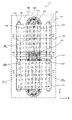
- FIG. 7 shows a plan view of the nitride semiconductor device 410 of the modified example of the second embodiment
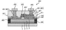
- FIG. 8 shows a cross-sectional view of the PN diode 490 which is a component thereof.
- a protection diode 492 configured by connecting a PN diode 490 in series is inserted between the gate and source of the nitride semiconductor device 310 in the second embodiment.
- the protection diode 492 is manufactured and integrated on the same chip as the FET by the same manufacturing process as the FET.
- a buffer layer 2 composed of an AlN layer and an AlGaN layer, a GaN channel layer 3, and an AlGaN barrier layer 4 are formed as a semiconductor laminate structure by epitaxial growth on a Si substrate 1.
- a p-type GaN layer 405 that has been epitaxially grown and then etched is formed.
- a high-concentration two-dimensional electron gas (not shown) is formed due to the effects of piezoelectric polarization and spontaneous polarization.
- the region in which the resistance of the two-dimensional electron gas is increased by ion implantation is the device separation region 409.
- a SiN film 441 is formed on the surfaces of the AlGaN barrier layer 4 and the p-type GaN layer 405 as a surface protective film, and the SiN film 441 is opened to form a dummy electrode 411 and a cathode electrode 413. Further, a SiO film is formed as the first dielectric film 443 on the SiN film 441.
- the anode electrode 425 is formed on the p-type GaN layer 405 by opening the SiN film 441 and the first dielectric film 443. The anode electrode 425 extends above the dummy electrode 411.
- a SiO film which is a second dielectric film 447, is formed on the anode electrode 425 and the cathode electrode 413.
- a via 451 on the cathode electrode 413 and a via 461 on the anode electrode 425 are formed by a conventional photolithography technique and a technique for dry etching the second dielectric film 447 and the first dielectric film 443.
- plugs 453 and 463 for filling the respective vias are formed. W (tungsten) is used for the portions of the plugs 453 and 463 in contact with the second dielectric film 447, with the TiN film as a barrier layer.
- the plug 453 is connected to the cathode electrode lead-out wire 455, and the plug 463 is connected to the anode lead-out wire 465.
- FIG. 7 shows a nitride semiconductor device 410 in which a protection diode 492 is electrically inserted between the source and gate.
- the protection diode 492 has five PN diodes 490 shown in FIG. 8 connected in series. Each PN diode 490 is formed in a second active region 498 surrounded by a device separation region 409 that is highly resistant by ion implantation. Further, the five PN diodes 490 are electrically connected in series by the anode-cathode wiring 483.
- the protection diode 492 is connected to the first source lead-out wire 355 by the anode-source wire 481 and is connected to the first gate lead-out wire 365 or the gate pad 393 by the cathode-gate wire 485.
- the dielectric breakdown voltage of the SiO film is about 3 MV / cm, and the dielectric breakdown voltage when the thickness of the SiO film (not shown) between the source electrode 311 and the gate electrode connecting portion 325 in FIG. 7 is 0.1 ⁇ m. Is 30V.
- the rising voltage of the GaN PN diode is about 3.5V. Since five PN diodes 490 are connected in series to the protection diode 492 of the nitride semiconductor device 310 in the present embodiment, a current flows when a reverse bias of about 17.5 V is applied between the source and the gate. That is, with a sufficient voltage margin, the dielectric breakdown between the gate electrode connecting portion 325 and the source electrode 311 is not dielectrically broken, and the source gate of the nitride semiconductor device 410 is protected.
- the area of the element separation region 409 is increased by the protection diode 492 as compared with the nitride semiconductor device 310, and as a result, the chip area is slightly increased.
- the protection diode 492 can be designed to have a smaller area than the FET which is a power transistor, the increase in the chip area is small.
- the number of PN diodes connected in series is 5, but the quantity is appropriately designed, for example, 3 to 10 depending on the required protection voltage. It is possible to do.
- the ratio of the first active region 408 to the chip area is smaller than that in the nitride semiconductor device 310 in the second embodiment, but it is sufficient as compared with the case where the POE technique is not used. Is big. As a result, the on-resistance is small and the chip area is small.
- the diode semiconductor device has a second active region surrounded by an element separation region on the substrate, and is formed in the second active region.
- a protection diode is formed in which a plurality of these diodes are connected in series, the anode of the protection diode is electrically connected to the source electrode, and the cathode of the protection diode is electrically connected to the gate electrode connection portion.
- the rising voltage of the current flowing from the anode to the cathode of the protection diode is lower than the insulation breakdown voltage of the first dielectric film.
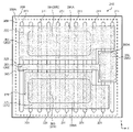
- FIG. 3 is plan views showing the nitride semiconductor device 510 according to the third embodiment of the present disclosure.
- 10 is an enlarged view of the dotted line portion M in FIG. 9, and
- FIG. 11 is an enlarged view of the dotted line portion N in FIG.
- the wiring layer is omitted in order to explain the portion of the FET under the wiring layer.
- FIG. 11 has the same configuration as that of the first embodiment.
- the first gate electrode 521 and the second gate electrode 523 are each coupled by a gate electrode connecting portion 525 at the central portion thereof.
- the gate electrode connecting portion 525 is formed of the same metal layer as the first gate electrode 521 and the second gate electrode 523 at the same time. Therefore, the number of manufacturing processes does not increase.
- the gate electrode connecting portion 525 is a SiO film which is a first dielectric film. It is formed on (not shown) and is electrically isolated from the source electrode 511.
- the width of the gate electrode connecting portion 525 is about 3 ⁇ m, and the length is designed to be larger than that of the first gate electrode 521 and the second gate electrode 523, which are about 1 ⁇ m in length. This design allows for the back end of line using vias and plugs described below, which is difficult on gate electrodes.
- a SiO film (not shown), which is a second dielectric film, is placed on the first gate electrode 521, the second gate electrode 523, the gate electrode connecting portion 525, the source electrode 511, and the drain electrodes 531 and 533. It is formed.
- the SiO film is designed to have a thickness that prevents dielectric breakdown between the source and drain. For example, in a 600V withstand voltage transistor, the thickness of the SiO film is 2 ⁇ m to 3 ⁇ m.
- the via 551 on the source electrode 511 can be obtained by ordinary photolithography technology and dry etching technology for the SiO film.
- Vias 561 on the gate electrode connecting portion 525 and vias 571 on the drain electrodes 531 and 533 are formed.
- plugs 553, 563, and 573 that fill the respective vias are formed.
- W tungsten
- the plug 555 is connected to the first source lead-out wire 555
- the plug 563 is connected to the first gate lead-out wire 565
- the plug 573 is connected to the first drain lead-out wire 575.
- a SiO film (not shown) is formed as a third dielectric film on the first source lead-out wiring 555, the first gate lead-out wiring 565, and the first drain lead-out wiring 575. Similar to the above, by the photolithography technique and the technique of dry etching the third dielectric film, the via 581 on the first source lead wire, the via 583 on the first gate lead wire, and the first drain lead wire are used. The upper via 585 is formed.
- plugs 582, 584, and 586 for filling the respective vias are formed.
- W tungsten
- the plug 582 is connected to the second source lead-out wire 587
- the plug 584 is connected to the second gate lead-out wire 588
- the plug 586 is connected to the second drain lead-out wire 589.
- the first source lead-out wiring 555 is sandwiched between the first gate lead-out wiring 565, and the drain lead-out wiring 575 is sandwiched between the first gate lead-out wiring 565.
- the gate wiring resistance is lowered, and at the same time, the drain lead-out wiring 575 to which a high voltage is applied is not arranged at the chip end, so that the reliability regarding moisture resistance is improved.
- the distance W2 between the first drain outlet wiring 575 and the first gate outlet wiring 565 is larger than the distance W1 between the first source outlet wiring 555 and the first gate outlet wiring 565.
- the second gate lead-out wiring 588 extends in the Y direction to form a gate pad 593 having a large area at its end.
- the gate pad 593 has a gate pad opening 593A formed with respect to a surface protective film (not shown) of the nitride semiconductor device 510.
- the second source lead-out wiring 587 extends in the Y direction, and the vicinity of the central portion thereof serves as a source pad 591.
- the source pad 591 has a source pad opening 591A formed with respect to a surface protective film (not shown) of the nitride semiconductor device 510.
- the second drain lead-out wiring 589 extends in the Y direction and becomes a drain pad 595 in the vicinity of the central portion thereof.
- the drain pad 595 has a drain pad opening 595A formed with respect to a surface protective film (not shown) of the nitride semiconductor device 510.
- the first active region 508, the device separation region 509, and the boundary 508A of the ion implantation region, which is the boundary between the two, are provided.
- the nitride semiconductor device 510 since the ratio of the first active region 508 to the chip area is high, the on-resistance is small and the chip area is small.
- the second gate lead-out wiring 588, the second source lead-out wiring 587, and the second drain lead-out wiring 589 are formed of the same metal layer. Therefore, the manufacturing process becomes simple.
- the same metal layer are Al (aluminum), Cu (copper), and Au (gold).
- Cu aluminum
- Cu copper
- Au gold
- each pad is formed by using only one wiring layer, but in the present embodiment, two wiring layers are used.
- each of the source / drain gates is compared with the case where only one wiring layer is used.
- Wiring resistance can be lowered.
- the wiring resistance of the gate uses two wiring layers, it is possible to significantly reduce the wiring resistance as compared with the examples of Cited Document 2 and the like. Further, since it is not necessary to form the gate wiring in the element separation region 509, the chip area is also reduced.
- the first gate lead-out wiring, the first source lead-out wiring, and the first drain lead-out wiring, and the first gate lead-out wiring is described.
- a third dielectric film is formed on the wiring, the first source lead-out wiring, and the first drain lead-out wiring, and a plurality of the said firsts are formed through vias formed on the third dielectric film.
- the second gate lead-out wiring extending in the second direction by electrically connecting the gate lead-out wiring of 1 and the plurality of the first source lead-out wirings are electrically connected in the second direction. It has a second source outlet wiring to be extended and a second drain outlet wiring to electrically connect a plurality of the first drain extraction wirings and extend in the second direction.
- the resistance of each lead-out wiring of the source / drain gate can be lowered as compared with the case where the wiring layer is one layer.
- the two wiring layers of the first gate lead-out wiring and the second gate lead-out wiring are used, there is an effect that the wiring resistance of the gate can be reduced.
- it is not necessary to form the gate lead-out wiring in the element separation region there is an effect that the chip area can be reduced.
- both sides of the first source lead-out wiring may be sandwiched by the first gate lead-out wiring, and the first drain lead-out wiring may be sandwiched by the first gate lead-out wiring.
- the drain lead-out wiring to which a high voltage is applied is not arranged at the chip end, so that the reliability regarding moisture resistance can be improved.
- the distance between the first drain withdrawal wiring and the first gate withdrawal wiring may be larger than the distance between the first source withdrawal wiring and the first gate withdrawal wiring.
- the electric field in the vicinity of the first drain lead-out wiring to which a high voltage is applied can be weakened, and the reliability regarding moisture resistance can be improved.
- the second gate lead-out wiring, the second source lead-out wiring, and the second drain lead-out wiring may be formed of the same metal wiring layer.
- the manufacturing process for forming the second gate lead-out wiring, the second source lead-out wiring, and the second drain lead-out wiring can be simplified.
- FIGS. 13A, 13B, 13C, and 13D are XIIIa-XIIIa line, XIIIb-XIIIb line, XIIIc-XIIIc line, and XIIId- in FIG. A cross-sectional view of the XIIId line is shown.
- the present embodiment is a double gate transistor having two gates.
- a buffer layer 2 composed of an AlN layer and an AlGaN layer, a GaN channel layer 3, and an AlGaN barrier layer 4 are formed as a semiconductor laminate structure on a Si substrate 1 by epitaxial growth. It is formed.
- p-type GaN layers 605, 606, 607, and 608 that have been epitaxially grown and then etched are formed.
- a high-concentration two-dimensional electron gas (not shown) is formed due to the effects of piezoelectric polarization and spontaneous polarization.
- the region where the two-dimensional electron gas is formed is the active region 609 of FIG. 12, and the region where the two-dimensional electron gas is made highly resistant by ion implantation is the device separation region 610.
- the boundary between the two is the boundary 609A of the ion implantation region.
- the element separation region 610 may be formed by removing the region containing the two-dimensional electron gas by mesa etching.
- a SiN film 641 is formed on the surfaces of the AlGaN barrier layer 4 and the p-type GaN layers 605, 606, 607, and 608 as surface protective films, and the SiN film 641 is formed.
- the first source electrode 631 and the second source electrode 633 are formed by opening.
- a SiO film is formed on the SiN film 641 as the first dielectric film 643.
- the SiN film 641 and the first dielectric film 643 are opened so that the first gate electrode 621, the second gate electrode 622, the third gate electrode 625, and the fourth gate electrode 626 are the p-type GaN layer 605. It is formed on 606, 607, and 608, respectively.
- the first gate electrode 621 and the second gate electrode 622 are formed at positions on both sides separated from each other in the X direction with respect to the finger-shaped first source electrode 631. Further, the third gate electrode 625 and the fourth gate electrode 626 are formed at positions on both sides separated from the finger-shaped second source electrode 633 in the X direction.
- first gate electrode 621 and the second gate electrode 622 are finger-shaped in the Y direction, which is a direction perpendicular to the X direction, together with the p-type GaN layer 605 and the p-type GaN layer 606 at the lower portions thereof. It is stretched and connected in an arc shape at both ends. With this configuration, the leakage current flowing between the first source electrode 631 and the second source electrode 633 in the off state is reduced.
- the finger-shaped gate electrode needs to reach the device separation region 610 beyond the boundary 609A of the ion implantation region. The same applies to the third gate electrode 625 and the fourth gate electrode 626.
- the first gate electrode 621 and the second gate electrode 622 are each coupled by the first gate electrode connecting portion 623 near the center thereof.
- the first gate electrode connecting portion 623 is formed of the same metal layer as the first gate electrode 621 and the second gate electrode 622 at the same time. Therefore, the number of manufacturing processes does not increase.
- the first gate electrode connecting portion 623 is the first dielectric. It is formed on the SiO film which is the body film 643, and is electrically insulated from the first source electrode 631.
- the width (depth direction of the paper surface) of the first gate electrode connecting portion 623 is about 3 ⁇ m, which is designed to be larger than the first gate electrode 621 and the second gate electrode 622 having a length of about 1 ⁇ m. .. This design allows for the back end of line using vias and plugs described below, which is difficult on gate electrodes.
- the third gate electrode 625 and the fourth gate electrode 626 are each coupled by a second gate electrode connecting portion 627 near the center thereof.
- SiO film which is a second dielectric film 647, is formed on the electrodes 631 and the second source electrode 633.
- the second dielectric film 647 is designed to have a thickness that prevents dielectric breakdown between the first source and the second source in the double gate transistor for high withstand voltage. For example, in the 600V withstand voltage double gate transistor, when the second dielectric film 647 is SiO, the thickness thereof is set to 2 ⁇ m to 3 ⁇ m.
- the width of the first source electrode 631, the first gate electrode connecting portion 623, the second gate electrode connecting portion 627, and the second source electrode 633 is about 3 ⁇ m
- the normal photolithography technique and the first Via 681 on the first source electrode 631, via 671 on the first gate electrode connecting portion 623, and the second source electrode by the technique of dry etching the dielectric film 647 of 2 and the first dielectric film 643.
- a via 651 on 633 and a via 661 on a second gate electrode connecting portion 627 are formed.
- plugs 683, 673, 653, and 663 that fill the respective vias are formed.
- W tungsten
- the plug 683 is connected to the lead wire 685 of the first source electrode
- the plug 673 is connected to the lead wire 675 of the first gate electrode
- the plug 653 is connected to the lead wire 655 of the second source electrode
- the plug 663 is connected. Is connected to the lead-out wiring 665 of the second gate electrode.
- the first gate electrode 621 and the second gate electrode 622 are connected by the first gate electrode connecting portion 623 at the central portion. Then, a via 671 is formed in the first gate electrode connecting portion 623 to perform gate wiring. Further, the third gate electrode 625 and the fourth gate electrode 626 are connected by a second gate electrode connecting portion 627 at the central portion. Then, a via 671 is formed in the first gate electrode connecting portion 623 and a via 661 is formed in the second gate electrode connecting portion 627 to perform gate wiring. Therefore, the gate wiring resistance is significantly reduced as compared with the case where the gate wiring is performed from the end of the gate electrode. Further, the gate wiring is formed not on the element separation region 610 but on the active region 609. As a result, the chip area does not increase.
- the side surface where the first source electrode 631 and the second source electrode 633 are in contact with the first dielectric film 643 has a cross section.
- the shape may be a forward taper. Due to the shape of the forward taper, the coverage with respect to the side surfaces of the first source electrode 631 and the second source electrode 633 of the first dielectric film 643 is improved, and voids (voids) and seams (seam) are not generated. As a result, a reverse bias voltage of several tens of volts was applied between the first source electrode 631 and the first gate electrode connecting portion 623, and between the second source electrode 633 and the second gate electrode connecting portion 627. Even in this case, there is an effect that the first dielectric film 643 is unlikely to undergo dielectric breakdown.
- a low resistance metal layer serving as a field plate electrode is placed on the first source electrode 631 and the second source electrode 633. May be provided.
- the configuration of FIG. 12 is repeatedly formed in the X direction, and the first source pad is formed in the lead-out wiring 685 of the first source electrode.
- the second source and the second are A protection diode may be inserted between the gates.
- the first source pad, the second source pad, the first gate pad, and the first source pad are used by using the wiring technique of the second layer as in the third embodiment. 2 gate pads may be formed.
- the nitride semiconductor device has a substrate, a semiconductor laminated structure composed of a plurality of nitride semiconductor layers on the substrate, and an element separation region around the upper surface side of the semiconductor laminated structure.
- a first active region surrounded by, and a first source electrode located on both sides of the first active region separated from the first source electrode in the first direction in a plan view.
- the first gate electrode, the second gate electrode, the second source electrode, the third gate electrode and the fourth gate electrode located on both sides of the second source electrode separated in the first direction in a plan view.
- the first source electrode, the first gate electrode, the second gate electrode, the second source electrode, the third gate electrode, and the fourth gate electrode have a gate electrode.
- the finger-shaped portion has a finger-shaped portion extending in a second direction perpendicular to the first direction in a plan view, and a first dielectric film is formed on the first source electrode and the second source electrode.
- the first gate electrode and the second gate electrode are electrically connected by a first gate electrode connecting portion formed on the first dielectric film, and the third gate is formed.
- the electrode and the fourth gate electrode are electrically connected by a second gate electrode connecting portion formed on the first dielectric film.
- the wiring length can be shortened and the wiring resistance of the gate can be reduced.
- the wiring resistance of the gate can be reduced.
- the first gate electrode, the second gate electrode, the first gate electrode connecting portion, the third gate electrode, the fourth gate electrode, and the second gate electrode connecting portion are the same. It may be formed of the metal layer of.
- the first gate electrode, the second gate electrode, the first gate electrode connecting portion, the third gate electrode, the fourth gate electrode, and the second gate electrode connecting portion It has the effect of not increasing the manufacturing process.
- the width of the first gate electrode connecting portion is larger than the length of the first gate electrode and the length of the second gate electrode, and the width of the second gate electrode connecting portion is the width of the third gate. It may be larger than the electrode length and the fourth gate electrode length.
- the portion in contact with the first dielectric film has a forward taper shape
- the portion in contact with the first dielectric film is formed. It may have a forward taper shape.
- the coverage of the first dielectric film with respect to the side surfaces of the first and second source electrodes is improved, and the generation of voids (voids) and seams (seam) is suppressed.
- a reverse bias voltage for example, several tens of volts
- the present disclosure is not limited to this embodiment. As long as it does not deviate from the gist of the present disclosure, various modifications that can be conceived by those skilled in the art are applied to this embodiment, and a form constructed by combining components in different embodiments is also within the scope of one or more embodiments. May be included within.
- the nitride semiconductor device in the nitride semiconductor device according to the present disclosure, it can be used as a switching transistor having a low gate wiring resistance.
Landscapes
- Junction Field-Effect Transistors (AREA)
Priority Applications (2)
| Application Number | Priority Date | Filing Date | Title |
|---|---|---|---|
| JP2022556427A JP7689297B2 (ja) | 2020-10-16 | 2021-08-16 | 窒化物半導体装置 |
| US18/246,280 US20230361179A1 (en) | 2020-10-16 | 2021-08-16 | Nitride semiconductor device |
Applications Claiming Priority (2)
| Application Number | Priority Date | Filing Date | Title |
|---|---|---|---|
| JP2020-174945 | 2020-10-16 | ||
| JP2020174945 | 2020-10-16 |
Publications (1)
| Publication Number | Publication Date |
|---|---|
| WO2022079995A1 true WO2022079995A1 (ja) | 2022-04-21 |
Family
ID=81207917
Family Applications (1)
| Application Number | Title | Priority Date | Filing Date |
|---|---|---|---|
| PCT/JP2021/029951 Ceased WO2022079995A1 (ja) | 2020-10-16 | 2021-08-16 | 窒化物半導体装置 |
Country Status (3)
| Country | Link |
|---|---|
| US (1) | US20230361179A1 (https=) |
| JP (1) | JP7689297B2 (https=) |
| WO (1) | WO2022079995A1 (https=) |
Citations (6)
| Publication number | Priority date | Publication date | Assignee | Title |
|---|---|---|---|---|
| JP2009123932A (ja) * | 2007-11-15 | 2009-06-04 | Nec Corp | 半導体装置およびその製造方法 |
| JP2013058640A (ja) * | 2011-09-08 | 2013-03-28 | Toshiba Corp | 半導体装置 |
| JP2016139718A (ja) * | 2015-01-28 | 2016-08-04 | 株式会社東芝 | 半導体装置 |
| JP2018088473A (ja) * | 2016-11-29 | 2018-06-07 | 日亜化学工業株式会社 | 電界効果トランジスタ |
| JP2019512886A (ja) * | 2016-03-17 | 2019-05-16 | クリー インコーポレイテッドCree Inc. | バイパスされたゲート構造を有するトランジスタ |
| JP2020068343A (ja) * | 2018-10-26 | 2020-04-30 | 株式会社東芝 | 半導体装置 |
Family Cites Families (6)
| Publication number | Priority date | Publication date | Assignee | Title |
|---|---|---|---|---|
| JPH04171734A (ja) * | 1990-11-02 | 1992-06-18 | Mitsubishi Electric Corp | 半導体装置 |
| JP3712111B2 (ja) | 2001-03-30 | 2005-11-02 | ユーディナデバイス株式会社 | 電力増幅用半導体装置 |
| JP2003168736A (ja) | 2001-11-30 | 2003-06-13 | Hitachi Ltd | 半導体素子及び高周波電力増幅装置並びに無線通信機 |
| JP5584090B2 (ja) | 2010-10-22 | 2014-09-03 | トランスフォーム・ジャパン株式会社 | Dc−dcコンバータ |
| US20130313653A1 (en) | 2012-05-25 | 2013-11-28 | Infineon Technologies Austria Ag | MOS Transistor with Multi-finger Gate Electrode |
| US10615273B2 (en) | 2017-06-21 | 2020-04-07 | Cree, Inc. | Semiconductor devices having a plurality of unit cell transistors that have smoothed turn-on behavior and improved linearity |
-
2021
- 2021-08-16 JP JP2022556427A patent/JP7689297B2/ja active Active
- 2021-08-16 US US18/246,280 patent/US20230361179A1/en active Pending
- 2021-08-16 WO PCT/JP2021/029951 patent/WO2022079995A1/ja not_active Ceased
Patent Citations (6)
| Publication number | Priority date | Publication date | Assignee | Title |
|---|---|---|---|---|
| JP2009123932A (ja) * | 2007-11-15 | 2009-06-04 | Nec Corp | 半導体装置およびその製造方法 |
| JP2013058640A (ja) * | 2011-09-08 | 2013-03-28 | Toshiba Corp | 半導体装置 |
| JP2016139718A (ja) * | 2015-01-28 | 2016-08-04 | 株式会社東芝 | 半導体装置 |
| JP2019512886A (ja) * | 2016-03-17 | 2019-05-16 | クリー インコーポレイテッドCree Inc. | バイパスされたゲート構造を有するトランジスタ |
| JP2018088473A (ja) * | 2016-11-29 | 2018-06-07 | 日亜化学工業株式会社 | 電界効果トランジスタ |
| JP2020068343A (ja) * | 2018-10-26 | 2020-04-30 | 株式会社東芝 | 半導体装置 |
Also Published As
| Publication number | Publication date |
|---|---|
| US20230361179A1 (en) | 2023-11-09 |
| JPWO2022079995A1 (https=) | 2022-04-21 |
| JP7689297B2 (ja) | 2025-06-06 |
Similar Documents
| Publication | Publication Date | Title |
|---|---|---|
| CN103325828B (zh) | 氮化物半导体元件 | |
| JP7539447B2 (ja) | 半導体装置 | |
| US10950524B2 (en) | Heterojunction semiconductor device for reducing parasitic capacitance | |
| US12211839B2 (en) | Nitride semiconductor device | |
| JP4645313B2 (ja) | 半導体装置 | |
| US9654001B2 (en) | Semiconductor device | |
| TW201705445A (zh) | 半導體裝置 | |
| US9035320B2 (en) | Semiconductor device | |
| JPWO2014050054A1 (ja) | 半導体装置 | |
| US20190267467A1 (en) | Semiconductor device | |
| JP6584987B2 (ja) | 半導体装置 | |
| JP2016009774A (ja) | 半導体装置 | |
| JP7313197B2 (ja) | 半導体装置 | |
| JP7476062B2 (ja) | 半導体装置 | |
| WO2022079995A1 (ja) | 窒化物半導体装置 | |
| TWI584467B (zh) | 半導體裝置 | |
| CN106373996A (zh) | 半导体装置 | |
| JP7387567B2 (ja) | 半導体装置 | |
| US12451468B1 (en) | III-N devices with improved reliability | |
| US20240313059A1 (en) | Nitride semiconductor device and nitride semiconductor module | |
| TWI660506B (zh) | 半導體裝置 | |
| WO2023157452A1 (ja) | 窒化物半導体装置 | |
| JP2026036979A (ja) | 窒化物半導体装置 | |
| CN116230703A (zh) | 半导体装置 |
Legal Events
| Date | Code | Title | Description |
|---|---|---|---|
| 121 | Ep: the epo has been informed by wipo that ep was designated in this application |
Ref document number: 21879737 Country of ref document: EP Kind code of ref document: A1 |
|
| ENP | Entry into the national phase |
Ref document number: 2022556427 Country of ref document: JP Kind code of ref document: A |
|
| NENP | Non-entry into the national phase |
Ref country code: DE |
|
| 122 | Ep: pct application non-entry in european phase |
Ref document number: 21879737 Country of ref document: EP Kind code of ref document: A1 |