WO2022079995A1 - 窒化物半導体装置 - Google Patents
窒化物半導体装置 Download PDFInfo
- Publication number
- WO2022079995A1 WO2022079995A1 PCT/JP2021/029951 JP2021029951W WO2022079995A1 WO 2022079995 A1 WO2022079995 A1 WO 2022079995A1 JP 2021029951 W JP2021029951 W JP 2021029951W WO 2022079995 A1 WO2022079995 A1 WO 2022079995A1
- Authority
- WO
- WIPO (PCT)
- Prior art keywords
- gate electrode
- gate
- source
- electrode
- lead
- Prior art date
Links
- 239000004065 semiconductor Substances 0.000 title claims abstract description 119
- 150000004767 nitrides Chemical class 0.000 title claims abstract description 98
- 238000000926 separation method Methods 0.000 claims abstract description 33
- 229910052751 metal Inorganic materials 0.000 claims description 40
- 239000002184 metal Substances 0.000 claims description 40
- 239000000758 substrate Substances 0.000 claims description 20
- 230000015556 catabolic process Effects 0.000 claims description 14
- WABPQHHGFIMREM-UHFFFAOYSA-N lead(0) Chemical compound [Pb] WABPQHHGFIMREM-UHFFFAOYSA-N 0.000 claims description 14
- 230000000630 rising effect Effects 0.000 claims description 3
- JMASRVWKEDWRBT-UHFFFAOYSA-N Gallium nitride Chemical compound [Ga]#N JMASRVWKEDWRBT-UHFFFAOYSA-N 0.000 description 50
- 229910002601 GaN Inorganic materials 0.000 description 49
- 230000000694 effects Effects 0.000 description 31
- 230000004888 barrier function Effects 0.000 description 26
- 229910002704 AlGaN Inorganic materials 0.000 description 24
- 238000000034 method Methods 0.000 description 19
- 230000004048 modification Effects 0.000 description 19
- 238000012986 modification Methods 0.000 description 19
- 238000004519 manufacturing process Methods 0.000 description 17
- 230000005533 two-dimensional electron gas Effects 0.000 description 15
- 238000005468 ion implantation Methods 0.000 description 13
- 239000010949 copper Substances 0.000 description 12
- 230000001681 protective effect Effects 0.000 description 11
- 230000010287 polarization Effects 0.000 description 9
- ATJFFYVFTNAWJD-UHFFFAOYSA-N Tin Chemical compound [Sn] ATJFFYVFTNAWJD-UHFFFAOYSA-N 0.000 description 6
- 238000001312 dry etching Methods 0.000 description 6
- 238000000206 photolithography Methods 0.000 description 6
- WFKWXMTUELFFGS-UHFFFAOYSA-N tungsten Chemical compound [W] WFKWXMTUELFFGS-UHFFFAOYSA-N 0.000 description 6
- 229910052721 tungsten Inorganic materials 0.000 description 6
- 239000010937 tungsten Substances 0.000 description 6
- 238000005530 etching Methods 0.000 description 5
- 230000002441 reversible effect Effects 0.000 description 5
- 230000002269 spontaneous effect Effects 0.000 description 5
- RYGMFSIKBFXOCR-UHFFFAOYSA-N Copper Chemical compound [Cu] RYGMFSIKBFXOCR-UHFFFAOYSA-N 0.000 description 4
- 229910052782 aluminium Inorganic materials 0.000 description 4
- XAGFODPZIPBFFR-UHFFFAOYSA-N aluminium Chemical compound [Al] XAGFODPZIPBFFR-UHFFFAOYSA-N 0.000 description 4
- 229910052802 copper Inorganic materials 0.000 description 4
- 230000009977 dual effect Effects 0.000 description 4
- 230000005684 electric field Effects 0.000 description 4
- 239000010931 gold Substances 0.000 description 4
- 230000015572 biosynthetic process Effects 0.000 description 3
- PCHJSUWPFVWCPO-UHFFFAOYSA-N gold Chemical compound [Au] PCHJSUWPFVWCPO-UHFFFAOYSA-N 0.000 description 2
- 229910052737 gold Inorganic materials 0.000 description 2
- 239000000463 material Substances 0.000 description 2
- 230000002040 relaxant effect Effects 0.000 description 2
- 238000000605 extraction Methods 0.000 description 1
- 230000005669 field effect Effects 0.000 description 1
- 238000010438 heat treatment Methods 0.000 description 1
- 238000002347 injection Methods 0.000 description 1
- 239000007924 injection Substances 0.000 description 1
- 238000009413 insulation Methods 0.000 description 1
- 230000002250 progressing effect Effects 0.000 description 1
- 238000004904 shortening Methods 0.000 description 1
Images


Classifications
-
- H—ELECTRICITY
- H01—ELECTRIC ELEMENTS
- H01L—SEMICONDUCTOR DEVICES NOT COVERED BY CLASS H10
- H01L29/00—Semiconductor devices specially adapted for rectifying, amplifying, oscillating or switching and having potential barriers; Capacitors or resistors having potential barriers, e.g. a PN-junction depletion layer or carrier concentration layer; Details of semiconductor bodies or of electrodes thereof ; Multistep manufacturing processes therefor
- H01L29/66—Types of semiconductor device ; Multistep manufacturing processes therefor
- H01L29/68—Types of semiconductor device ; Multistep manufacturing processes therefor controllable by only the electric current supplied, or only the electric potential applied, to an electrode which does not carry the current to be rectified, amplified or switched
- H01L29/76—Unipolar devices, e.g. field effect transistors
- H01L29/772—Field effect transistors
- H01L29/778—Field effect transistors with two-dimensional charge carrier gas channel, e.g. HEMT ; with two-dimensional charge-carrier layer formed at a heterojunction interface
- H01L29/7786—Field effect transistors with two-dimensional charge carrier gas channel, e.g. HEMT ; with two-dimensional charge-carrier layer formed at a heterojunction interface with direct single heterostructure, i.e. with wide bandgap layer formed on top of active layer, e.g. direct single heterostructure MIS-like HEMT
-
- H—ELECTRICITY
- H01—ELECTRIC ELEMENTS
- H01L—SEMICONDUCTOR DEVICES NOT COVERED BY CLASS H10
- H01L29/00—Semiconductor devices specially adapted for rectifying, amplifying, oscillating or switching and having potential barriers; Capacitors or resistors having potential barriers, e.g. a PN-junction depletion layer or carrier concentration layer; Details of semiconductor bodies or of electrodes thereof ; Multistep manufacturing processes therefor
- H01L29/02—Semiconductor bodies ; Multistep manufacturing processes therefor
- H01L29/12—Semiconductor bodies ; Multistep manufacturing processes therefor characterised by the materials of which they are formed
- H01L29/20—Semiconductor bodies ; Multistep manufacturing processes therefor characterised by the materials of which they are formed including, apart from doping materials or other impurities, only AIIIBV compounds
- H01L29/2003—Nitride compounds
-
- H—ELECTRICITY
- H01—ELECTRIC ELEMENTS
- H01L—SEMICONDUCTOR DEVICES NOT COVERED BY CLASS H10
- H01L23/00—Details of semiconductor or other solid state devices
- H01L23/48—Arrangements for conducting electric current to or from the solid state body in operation, e.g. leads, terminal arrangements ; Selection of materials therefor
- H01L23/481—Internal lead connections, e.g. via connections, feedthrough structures
-
- H—ELECTRICITY
- H01—ELECTRIC ELEMENTS
- H01L—SEMICONDUCTOR DEVICES NOT COVERED BY CLASS H10
- H01L29/00—Semiconductor devices specially adapted for rectifying, amplifying, oscillating or switching and having potential barriers; Capacitors or resistors having potential barriers, e.g. a PN-junction depletion layer or carrier concentration layer; Details of semiconductor bodies or of electrodes thereof ; Multistep manufacturing processes therefor
- H01L29/40—Electrodes ; Multistep manufacturing processes therefor
- H01L29/41—Electrodes ; Multistep manufacturing processes therefor characterised by their shape, relative sizes or dispositions
- H01L29/417—Electrodes ; Multistep manufacturing processes therefor characterised by their shape, relative sizes or dispositions carrying the current to be rectified, amplified or switched
- H01L29/41725—Source or drain electrodes for field effect devices
- H01L29/41775—Source or drain electrodes for field effect devices characterised by the proximity or the relative position of the source or drain electrode and the gate electrode, e.g. the source or drain electrode separated from the gate electrode by side-walls or spreading around or above the gate electrode
-
- H—ELECTRICITY
- H01—ELECTRIC ELEMENTS
- H01L—SEMICONDUCTOR DEVICES NOT COVERED BY CLASS H10
- H01L29/00—Semiconductor devices specially adapted for rectifying, amplifying, oscillating or switching and having potential barriers; Capacitors or resistors having potential barriers, e.g. a PN-junction depletion layer or carrier concentration layer; Details of semiconductor bodies or of electrodes thereof ; Multistep manufacturing processes therefor
- H01L29/40—Electrodes ; Multistep manufacturing processes therefor
- H01L29/41—Electrodes ; Multistep manufacturing processes therefor characterised by their shape, relative sizes or dispositions
- H01L29/423—Electrodes ; Multistep manufacturing processes therefor characterised by their shape, relative sizes or dispositions not carrying the current to be rectified, amplified or switched
- H01L29/42312—Gate electrodes for field effect devices
- H01L29/42316—Gate electrodes for field effect devices for field-effect transistors
-
- H—ELECTRICITY
- H01—ELECTRIC ELEMENTS
- H01L—SEMICONDUCTOR DEVICES NOT COVERED BY CLASS H10
- H01L29/00—Semiconductor devices specially adapted for rectifying, amplifying, oscillating or switching and having potential barriers; Capacitors or resistors having potential barriers, e.g. a PN-junction depletion layer or carrier concentration layer; Details of semiconductor bodies or of electrodes thereof ; Multistep manufacturing processes therefor
- H01L29/66—Types of semiconductor device ; Multistep manufacturing processes therefor
- H01L29/86—Types of semiconductor device ; Multistep manufacturing processes therefor controllable only by variation of the electric current supplied, or only the electric potential applied, to one or more of the electrodes carrying the current to be rectified, amplified, oscillated or switched
- H01L29/861—Diodes
- H01L29/8613—Mesa PN junction diodes
-
- H—ELECTRICITY
- H01—ELECTRIC ELEMENTS
- H01L—SEMICONDUCTOR DEVICES NOT COVERED BY CLASS H10
- H01L29/00—Semiconductor devices specially adapted for rectifying, amplifying, oscillating or switching and having potential barriers; Capacitors or resistors having potential barriers, e.g. a PN-junction depletion layer or carrier concentration layer; Details of semiconductor bodies or of electrodes thereof ; Multistep manufacturing processes therefor
- H01L29/66—Types of semiconductor device ; Multistep manufacturing processes therefor
- H01L29/86—Types of semiconductor device ; Multistep manufacturing processes therefor controllable only by variation of the electric current supplied, or only the electric potential applied, to one or more of the electrodes carrying the current to be rectified, amplified, oscillated or switched
- H01L29/861—Diodes
- H01L29/866—Zener diodes
-
- H—ELECTRICITY
- H01—ELECTRIC ELEMENTS
- H01L—SEMICONDUCTOR DEVICES NOT COVERED BY CLASS H10
- H01L29/00—Semiconductor devices specially adapted for rectifying, amplifying, oscillating or switching and having potential barriers; Capacitors or resistors having potential barriers, e.g. a PN-junction depletion layer or carrier concentration layer; Details of semiconductor bodies or of electrodes thereof ; Multistep manufacturing processes therefor
- H01L29/02—Semiconductor bodies ; Multistep manufacturing processes therefor
- H01L29/06—Semiconductor bodies ; Multistep manufacturing processes therefor characterised by their shape; characterised by the shapes, relative sizes, or dispositions of the semiconductor regions ; characterised by the concentration or distribution of impurities within semiconductor regions
- H01L29/10—Semiconductor bodies ; Multistep manufacturing processes therefor characterised by their shape; characterised by the shapes, relative sizes, or dispositions of the semiconductor regions ; characterised by the concentration or distribution of impurities within semiconductor regions with semiconductor regions connected to an electrode not carrying current to be rectified, amplified or switched and such electrode being part of a semiconductor device which comprises three or more electrodes
- H01L29/1066—Gate region of field-effect devices with PN junction gate
-
- H—ELECTRICITY
- H01—ELECTRIC ELEMENTS
- H01L—SEMICONDUCTOR DEVICES NOT COVERED BY CLASS H10
- H01L29/00—Semiconductor devices specially adapted for rectifying, amplifying, oscillating or switching and having potential barriers; Capacitors or resistors having potential barriers, e.g. a PN-junction depletion layer or carrier concentration layer; Details of semiconductor bodies or of electrodes thereof ; Multistep manufacturing processes therefor
- H01L29/40—Electrodes ; Multistep manufacturing processes therefor
- H01L29/402—Field plates
-
- H—ELECTRICITY
- H01—ELECTRIC ELEMENTS
- H01L—SEMICONDUCTOR DEVICES NOT COVERED BY CLASS H10
- H01L29/00—Semiconductor devices specially adapted for rectifying, amplifying, oscillating or switching and having potential barriers; Capacitors or resistors having potential barriers, e.g. a PN-junction depletion layer or carrier concentration layer; Details of semiconductor bodies or of electrodes thereof ; Multistep manufacturing processes therefor
- H01L29/40—Electrodes ; Multistep manufacturing processes therefor
- H01L29/41—Electrodes ; Multistep manufacturing processes therefor characterised by their shape, relative sizes or dispositions
- H01L29/417—Electrodes ; Multistep manufacturing processes therefor characterised by their shape, relative sizes or dispositions carrying the current to be rectified, amplified or switched
- H01L29/41725—Source or drain electrodes for field effect devices
- H01L29/41758—Source or drain electrodes for field effect devices for lateral devices with structured layout for source or drain region, i.e. the source or drain region having cellular, interdigitated or ring structure or being curved or angular
-
- H—ELECTRICITY
- H01—ELECTRIC ELEMENTS
- H01L—SEMICONDUCTOR DEVICES NOT COVERED BY CLASS H10
- H01L29/00—Semiconductor devices specially adapted for rectifying, amplifying, oscillating or switching and having potential barriers; Capacitors or resistors having potential barriers, e.g. a PN-junction depletion layer or carrier concentration layer; Details of semiconductor bodies or of electrodes thereof ; Multistep manufacturing processes therefor
- H01L29/40—Electrodes ; Multistep manufacturing processes therefor
- H01L29/41—Electrodes ; Multistep manufacturing processes therefor characterised by their shape, relative sizes or dispositions
- H01L29/423—Electrodes ; Multistep manufacturing processes therefor characterised by their shape, relative sizes or dispositions not carrying the current to be rectified, amplified or switched
Definitions
- the present disclosure relates to a nitride semiconductor device using a nitride semiconductor such as gallium nitride (GaN) as a semiconductor material.
- a nitride semiconductor such as gallium nitride (GaN) as a semiconductor material.
- GaN-FETs field effect transistors
- GaN which is a nitride semiconductor
- a GaN-FET a GaN layer is formed as a channel layer and AlGaN is formed as a barrier layer on a semiconductor substrate, and a two-dimensional electron gas generated by spontaneous polarization and piezopolarization at a heterojunction interface formed by these two layers. Is generally used as a channel.
- a channel current flows in a direction parallel to the substrate.
- the source pad, drain pad, and gate pad that supply voltage or pass current from the outside through wire bonding or the like to the FET are all formed on the surface side of the substrate. Therefore, in order to reduce the cost of the GaN-FET by reducing the chip area, it is important to reduce the pad area occupying the entire chip area.
- the wiring of the gate electrode is formed in the element separation region outside the active region.
- the gate electrode 8 is bundled outside the active region and further bypassed the outer periphery of the active region and connected to the gate electrode pad layer 23.” be.
- the present disclosure shows that by wiring the gate electrode on the active region, the wiring length to the gate electrode pad is shortened, and as a result, the wiring resistance of the gate is reduced, and the nitride suitable for high-speed switching operation is used.
- the main purpose is to provide semiconductor devices.
- a substrate a semiconductor laminated structure composed of a plurality of nitride semiconductor layers on the substrate, and an upper surface side of the semiconductor laminated structure.
- a first active region surrounded by an element separation region, a source electrode on the first active region, and a first located on both sides separated from the source electrode in the first direction in a plan view.
- the gate electrode 1, the second gate electrode, and the drain electrode have a finger-shaped portion extending in a second direction perpendicular to the first direction in a plan view, and a second gate electrode is placed on the source electrode.
- the dielectric film of 1 is formed, and the first gate electrode and the second gate electrode are electrically connected by a gate electrode connecting portion formed on the first dielectric film. ing.
- a substrate, a semiconductor laminated structure composed of a plurality of nitride semiconductor layers on the substrate, and the semiconductor laminate are used.
- a first active region surrounded by an element separation region, a first source electrode on the first active region, and a plan view of the first source electrode.
- the first gate electrode, the second gate electrode, the second source electrode, and the second source electrode located on both sides separated from each other in the first direction are separated from each other in the first direction in a plan view.
- the gate electrode, the fourth gate electrode has a finger-shaped portion extending in a second direction perpendicular to the first direction in a plan view, and is above the first source electrode and the second source electrode.
- a first dielectric film is formed in the semiconductor, and the first gate electrode and the second gate electrode are formed by a first gate electrode connecting portion formed on the first dielectric film. It is electrically connected, and the third gate electrode and the fourth gate electrode are electrically connected by a second gate electrode connecting portion formed on the first dielectric film.
- the present disclosure provides a nitride semiconductor device capable of reducing gate wiring resistance.
- FIG. 1 is a plan view of the nitride semiconductor device according to the first embodiment.
- FIG. 2A is a cross-sectional view taken along the line IIa-IIa of the nitride semiconductor device of FIG. 1 in the first embodiment.
- FIG. 2B is a cross-sectional view taken along the line IIb-IIb of the nitride semiconductor device of FIG. 1 in the first embodiment.
- FIG. 2C is a cross-sectional view taken along the line IIc-IIc of the nitride semiconductor device of FIG. 1 in the first embodiment.
- FIG. 3 is a cross-sectional view of the nitride semiconductor device according to the first modification of the first embodiment.
- FIG. 4 is a plan view of the nitride semiconductor device according to the second modification of the first embodiment.
- FIG. 5A is a cross-sectional view taken along the line Va—Va of the nitride semiconductor device of FIG. 4 in the second modification of the first embodiment.
- FIG. 5B is a cross-sectional view taken along the line Vb-Vb of the nitride semiconductor device of FIG. 4 in the second modification of the first embodiment.
- FIG. 5C is a cross-sectional view taken along the line Vc—Vc of the nitride semiconductor device of FIG. 4 in the second modification of the first embodiment.
- FIG. 6 is a plan view of the nitride semiconductor device according to the second embodiment.
- FIG. 7 is a plan view of the nitride semiconductor device in the modified example of the second embodiment.
- FIG. 8 is a cross-sectional view of a PN diode used in the nitride semiconductor device in the modified example of the second embodiment.
- FIG. 9 is a plan view of the nitride semiconductor device in the third embodiment.
- FIG. 10 is an enlarged plan view of the dotted line portion M in FIG. 9.
- FIG. 11 is an enlarged plan view of the dotted line portion N of FIG.
- FIG. 12 is a plan view of the nitride semiconductor device according to the fourth embodiment.
- FIG. 13A is a cross-sectional view taken along the line XIIIa-XIIIa of the nitride semiconductor device of FIG. 12 in the fourth embodiment.
- FIG. 13A is a cross-sectional view taken along the line XIIIa-XIIIa of the nitride semiconductor device of FIG. 12 in the fourth embodiment.
- FIG. 13B is a cross-sectional view taken along the line XIIIb-XIIIb of the nitride semiconductor device of FIG. 12 in the fourth embodiment.
- FIG. 13C is a cross-sectional view taken along the line XIIIc-XIIIc of the nitride semiconductor device of FIG. 12 in the fourth embodiment.
- FIG. 13D is a cross-sectional view taken along the line XIIId-XIIId of the nitride semiconductor device according to FIG. 12 in the fourth embodiment.
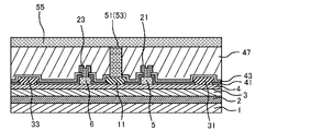
- FIG. 1 shows a plan view of the nitride semiconductor device 10 of the first embodiment
- FIGS. 2A, 2B, and 2C show cross-sectional views of the lines IIa-IIa, IIb-IIb, and IIc-IIc in FIG. ..
- a buffer layer 2 composed of an AlN layer and an AlGaN layer, a GaN channel layer 3, and an AlGaN barrier layer 4 are formed as a semiconductor laminate structure by epitaxial growth on a Si substrate 1. There is. On the AlGaN barrier layer 4, a p-type GaN layer 5 and a p-type GaN layer 6 that have been epitaxially grown on the AlGaN barrier layer 4 and then etched are formed. At the interface between the GaN channel layer 3 and the AlGaN barrier layer 4, a high-concentration two-dimensional electron gas is formed due to the effects of piezoelectric polarization and spontaneous polarization.
- the region in which the two-dimensional electron gas is formed is the first active region 8 shown in FIG. 1, and the region in which the resistance of the two-dimensional electron gas is increased by ion implantation is the device separation region 9.
- the boundary between the first active region 8 and the device separation region 9 is the boundary 8A of the ion implantation region.
- the element separation region 9 may be formed by removing the region containing the two-dimensional electron gas by mesa etching.
- a SiN film 41 is formed as a surface protective film on the surfaces of the AlGaN barrier layer 4, the p-type GaN layer 5, and the p-type GaN layer 6, and the SiN film 41 is opened.
- the source electrode 11, the drain electrode 31, and the drain electrode 33 are formed.
- a SiO film is formed on the SiN film 41 as the first dielectric film 43.
- the first gate electrode 21 and the second gate electrode 23 are formed by opening the SiN film 41 and the first dielectric film 43 on the p-type GaN layer 5 and the p-type GaN layer 6, respectively. ..
- the first gate electrode 21 and the second gate electrode 23 are formed at positions on both sides separated from the finger-shaped source electrode 11 in the first direction in a plan view.
- the first direction is the X direction in FIG.
- the finger-shaped drain electrode 31 is located in the direction opposite to the source electrode 11 with respect to the first gate electrode 21, and the finger-shaped drain electrode 33 and the source electrode 11 with respect to the second gate electrode 23.
- the first gate electrode 21 and the second gate electrode 23, together with the p-type GaN layer 5 and the p-type GaN layer 6 at the lower portions thereof, are in the second direction perpendicular to the first direction in a plan view. It is extended in a finger shape and connected in an arc shape at both ends.
- the second direction is the Y direction in FIG.
- the leakage current flowing between the source electrode 11, the drain electrode 31, and the drain electrode 33 in the off state is reduced.
- the finger-shaped gate electrode needs to exceed the boundary 8A of the ion implantation region and reach the element separation region 9. ..
- the first gate electrode 21 and the second gate electrode 23 are each coupled by a gate electrode connecting portion 25 at the central portion thereof.
- the gate electrode connecting portion 25 is formed of the same metal layer as the first gate electrode 21 and the second gate electrode 23 at the same time. Therefore, the number of manufacturing processes does not increase.
- the gate electrode connecting portion 25 is the first dielectric film 43. It is formed on the SiO film, which is electrically insulated from the source electrode 11.
- the width of the gate electrode connecting portion 25 (in the depth direction of the paper surface) is about 3 ⁇ m, and both are designed to be larger than the first gate electrode 21 and the second gate electrode 23 having a length of about 1 ⁇ m. This design enables a back end of line using vias and plugs, which is difficult on gate electrodes.
- a first gate electrode 21, a second gate electrode 23, a gate electrode connecting portion 25, a source electrode 11, a drain electrode 31 and a drain electrode 33 are placed on the first gate electrode 21 and the drain electrode 33.
- the SiO film which is the dielectric film 47 of 2 is formed.
- the second dielectric film 47 is designed to have a thickness that prevents dielectric breakdown between the source and drain in the high withstand voltage transistor. For example, in a 600V withstand voltage transistor, when the second dielectric film 47 is a SiO film, the thickness thereof is set to 2 ⁇ m to 3 ⁇ m.
- the widths of the source electrode 11, the gate electrode connecting portion 25, and the drain electrode 31 are all about 3 ⁇ m, the ordinary photo lithography technology and the second dielectric film 47 and the first dielectric film 43 are dried.
- a via 51 on the source electrode 11, a via 61 on the gate electrode connecting portion 25, and a via 71 on the drain electrode 31 and the drain electrode 33 are formed.
- plugs 53, 63, 73 for filling the respective vias are formed.
- W tungsten
- the plug 53 is connected to the first source lead wire 55
- the plug 63 is connected to the first gate lead wire 65
- the plug 73 is connected to the first drain lead wire 75.
- the first gate electrode 21 and the second gate electrode 23 are connected by a gate electrode connecting portion 25 at the central portion. Then, a via 61 is formed in the gate electrode connecting portion 25 to perform gate wiring. Therefore, the gate wiring resistance is significantly reduced as compared with the case where the gate wiring is performed from the end of the gate electrode.
- the nitride semiconductor device 10 is suitable for high-speed switching operation due to the decrease in gate wiring resistance.
- the gate wiring is formed not on the element separation region 9 but on the first active region 8. As a result, the chip area does not increase. Further, a capacitance is generated by the first dielectric film 43 between the source electrode 11 and the gate electrode connecting portion 25. This capacitance is the capacitance between the gate and source, but in order to prevent erroneous arcs in the power transistor for switching, it is desirable to increase the capacitance between the gate and source with respect to the capacitance between the gate and drain. Therefore, by using this embodiment, it is possible to realize a power transistor for switching, which has a large gate-source capacitance and can prevent an erroneous arc.
- W is used as the plug for filling the via in the nitride semiconductor device 10 in the present embodiment
- Al aluminum
- Cu copper
- the plug and the wiring connected to the plug may be formed at the same time by using the dual damascene method.
- the number of vias 61 on the gate electrode connecting portion 25 is one in FIG. 1, a plurality of vias 61 may be formed if possible from the viewpoint of manufacturing technology. Further, the number of vias 71 on the source electrodes 11 and the drain electrodes 31 and 33 should be large in order to reduce the wiring resistance, but it is appropriately designed from the viewpoint of the manufacturing technique for forming the vias and the plugs.
- the nitride semiconductor device has a substrate, a semiconductor laminated structure composed of a plurality of nitride semiconductor layers on the substrate, and an element separation region around the upper surface side of the semiconductor laminated structure.
- a first active region surrounded by, a source electrode on the first active region, a first gate electrode and a second gate electrode located on both sides separated from the source electrode in the first direction in a plan view. It has at least one drain electrode located in the direction opposite to the source electrode with respect to the gate electrode, the first gate electrode or the second gate electrode, and the source electrode, the first gate electrode, and the first gate electrode.
- the gate electrode 2 and the drain electrode have a finger-shaped portion extending in a second direction perpendicular to the first direction in a plan view, and a first dielectric film is formed on the source electrode.
- the first gate electrode and the second gate electrode are electrically connected by a gate electrode connecting portion formed on the first dielectric film.
- the wiring of the gate electrode (this wiring includes the finger-shaped portion) is formed inside the first active region instead of the outside in a plan view, thereby shortening the wiring length and wiring the gate.
- the resistance can be reduced.
- by forming the wiring of the gate electrode inside the active region in a plan view there is an effect that the area of the chip as a nitride semiconductor device can be reduced.
- the first gate electrode, the second gate electrode, and the gate electrode connecting portion may be formed of the same metal layer.
- the wiring resistance of the gate electrode can be reduced by the gate electrode connecting portion. Moreover, there is an effect that the manufacturing process is not increased in the formation of the first gate electrode, the second gate electrode and the gate electrode connecting portion.
- the width of the gate electrode connecting portion may be larger than the first gate electrode length and the second gate electrode length.
- FIG. 3 is a partial cross-sectional view of the nitride semiconductor device 110 showing a modified example of the first embodiment, and is an enlarged view of a portion corresponding to the vicinity of the source electrode 11 of FIG. 2B of the first embodiment. Drain electrodes, vias, plugs, wiring, etc. are omitted.
- a SiN film 141 is formed on the surfaces of the AlGaN barrier layer 4 and the p-type GaN layers 105 and 106 as a surface protective film, and the source electrode 111 is formed by opening the SiN film 141. Further, a SiO film is formed on the SiN film 141 as the first dielectric film 143.
- the SiN film 141 and the first dielectric film 143 are opened, and the first gate electrode 121 and the second gate electrode 123 are formed on the p-type GaN layers 105 and 106, respectively. Then, the first gate electrode 121 and the second gate electrode 123 are coupled by the gate electrode connecting portion 125.
- the cross-sectional shape of the side surface where the source electrode 111 is in contact with the first dielectric film 143 is a forward taper.
- the angle of the forward taper is preferably 45 ° or more and 75 ° or less, and more preferably 50 ° or more and 70 ° or less. This shape improves coverage of the first dielectric film 143 with respect to the side surface of the source electrode 111, and eliminates voids and seams. As a result, even when a reverse bias voltage of several tens of volts is applied between the source electrode 111 and the gate electrode connecting portion 125, there is an effect that the first dielectric film 143 is less likely to undergo dielectric breakdown.
- the forward taper cross-sectional shape in this modification can be realized by adding a forward taper to the cross-sectional shape by heat treatment of the resist that is the etching mask for dry etching.
- the portion of the side surface of the source electrode in contact with the first dielectric film has a forward taper shape.
- the coverage with respect to the side surface of the source electrode of the first dielectric film is improved, and the generation of voids (voids) and seams (seam) is suppressed.
- a reverse bias voltage for example, several tens of volts
- Modification 2 of Embodiment 1 4 is a plan view of the nitride semiconductor device 210 of the second modification of the first embodiment, and FIGS. 5A, 5B, and 5C are cross-sectional views of the Va-Va line, the Vb-Vb line, and the Vc-Vc line in FIG. Are shown respectively.
- a buffer layer 2 composed of an AlN layer and an AlGaN layer, a GaN channel layer 3, and an AlGaN barrier layer 4 are formed as a semiconductor laminate structure by epitaxial growth on a Si substrate 1. There is. On the AlGaN barrier layer 4, a p-type GaN layer 5 and a p-type GaN layer 6 that have been epitaxially grown and then etched are formed. At the interface between the GaN channel layer 3 and the AlGaN barrier layer 4, a high-concentration two-dimensional electron gas (not shown) is formed due to the effects of piezoelectric polarization and spontaneous polarization.
- the region where the two-dimensional electron gas is formed is the first active region 208 in FIG. 4, and the region where the resistance of the two-dimensional electron gas is increased by ion implantation is the device separation region 209.
- the boundary between the first active region 208 and the device separation region 209 is the boundary 208A of the ion implantation region.
- the element separation region 209 may be formed by removing the region containing the two-dimensional electron gas by mesa etching.
- a SiN film 241 is formed as a surface protective film on the surfaces of the AlGaN barrier layer 4, the p-type GaN layer 5, and the p-type GaN layer 6, and the SiN film 241 is opened.
- the source electrode 211 and the drain electrodes 231 and 233 are formed.
- a SiO film is formed as the first dielectric film 243 on the SiN film 241.
- the SiN film 241 and the first dielectric film 243 are opened, and the first gate electrode 221 and the second gate electrode 223 are formed on the p-type GaN layer 5 and the p-type GaN layer 6, respectively.
- the first gate electrode 221 and the second gate electrode 223 are formed at positions on both sides separated from each other in the X direction with respect to the finger-shaped source electrode 211.
- the finger-shaped drain electrode 231 is located in the direction opposite to the source electrode 211 with respect to the first gate electrode 221 and the finger-shaped drain electrode 233 is with respect to the source electrode 211 with respect to the second gate electrode 223. Located in the opposite direction.
- the finger-shaped gate electrode needs to exceed the boundary 208A of the ion implantation region and reach the device separation region 209. ..
- the first gate electrode 221 and the second gate electrode 223 are coupled by a gate electrode connecting portion 225 at their central portions.
- the gate electrode connecting portion 225 is formed of the same metal layer as the first gate electrode 221 and the second gate electrode 223 at the same time. Therefore, the number of manufacturing processes does not increase.
- the gate electrode connecting portion 225 is the first dielectric film 243. It is formed on the top and is electrically isolated from the source electrode 211.
- the width of the gate electrode connecting portion 225 (in the depth direction of the paper surface) is about 3 ⁇ m, and both are designed to be larger than the first gate electrode 221 and the second gate electrode 223 having a length of about 1 ⁇ m. This design enables a back end of line using vias and plugs, which is difficult on gate electrodes.
- a SiO film 245 is formed as a field plate film covering the first gate electrode 221 and the second gate electrode 223, the source electrode 211, and the drain electrodes 231 and 233.
- the SiO film 245 and the first dielectric film 243 are opened on the source electrode 211 to form a low resistance metal layer 285 to be a source field plate electrode.
- the low resistance metal layer 285 has the effect of relaxing the electric field concentration at the drain-side ends of the p-type GaN layer 5 and the p-type GaN layer 6.
- the withstand voltage is improved, and the phenomenon of current collapse, which is a problem in the nitride semiconductor device, is alleviated.
- the low resistance metal layer 285 is formed on the source electrode 211 other than the vicinity of the gate electrode connecting portion 225, it also has an effect of lowering the wiring resistance of the source electrode 211.
- the SiO film 245 and the first dielectric film 243 are opened on the drain electrode 231 and the drain electrode 233 to lower the resistance metal layer 281.
- Each of the resistance metal layers 283 is formed.
- the low resistance metal layer 281 and the low resistance metal layer 283 are formed entirely on the drain electrode 231 and the drain electrode 233, so that the wiring resistance of the drain electrode 231 and the drain electrode 233 can be reduced. It has the effect of lowering.
- a SiO film which is a second dielectric film 247, is formed on the low resistance metal layers 281, 283, 285, and 287.
- the second dielectric film 247 is designed to have a thickness that prevents dielectric breakdown between the source and drain in the high withstand voltage transistor.
- the thickness thereof is set to 2 ⁇ m to 3 ⁇ m.
- the low resistance metal is made by ordinary photolithography technology and dry etching technology for the second dielectric film 247.
- the plug 253 is connected to the first source lead wire 255, the plug 263 is connected to the first gate lead wire 265, and the plug 273 is connected to the first drain lead wire 275.
- the first gate electrode 221 and the second gate electrode 223 are connected by a gate electrode connecting portion 225 at the central portion. Then, a via 261 is formed in the gate electrode connecting portion 225 to perform gate wiring. Therefore, the gate wiring resistance is significantly reduced as compared with the case where the gate wiring is performed from the end of the gate electrode. Also, the gate wiring is formed not on the element separation region 209 but on the first active region 208. As a result, the chip area does not increase. Further, a capacitance is generated by the first dielectric film 243 between the source electrode 211 and the gate electrode connecting portion 225.
- This capacitance is the capacitance between the gate and source, but in order to prevent erroneous arcs in the power transistor for switching, it is desirable to increase the capacitance between the gate and source with respect to the capacitance between the gate and drain. Therefore, by using this embodiment, it is possible to realize a power transistor for switching, which has a large gate-source capacitance and can prevent an erroneous arc.
- W is used as the plug for filling the via in the nitride semiconductor device 210 in the present embodiment
- Al aluminum
- Cu copper
- the plug and the wiring connected to the plug may be formed at the same time by using the dual damascene method.
- the number of vias 261 on the low resistance metal layer 287 on the gate electrode connecting portion 225 is one, but a plurality of vias 261 may be formed if possible from the viewpoint of manufacturing technology. .. Further, the number of vias 271 on the source electrode 211 and the drain electrodes 231 and 233 should be large in order to reduce the wiring resistance, but it is appropriately designed from the viewpoint of the manufacturing technique for forming the via and the plug.
- a low resistance metal layer is formed on the source electrode excluding the lower part of the gate electrode connecting portion and on the drain electrode. ing.
- the low resistance metal layer is formed on the source electrode, it has the effect of lowering the wiring resistance of the source electrode. Further, since the low resistance metal layer is formed on the drain electrode, it has an effect of lowering the wiring resistance of the drain electrode.
- the low resistance metal layer formed on the source electrode is a source field plate electrode that extends above the first gate electrode and the second gate electrode in the direction of the drain electrode. There may be.
- the low resistance metal layer has the effect of relaxing the electric field concentration at the drain side end of the gate. As a result, the withstand voltage is improved and the phenomenon of current collapse is also alleviated.
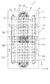
- FIG. 6 shows a plan view of the nitride semiconductor device 310 according to the second embodiment.
- the nitride semiconductor devices of the first embodiment or the modified examples 1 and 2 thereof are repeatedly arranged in the X direction shown in FIG. 6 to form a power transistor.
- FIG. 6 for the sake of simplification, components that are not particularly necessary for explaining the present embodiment are omitted.
- a plurality of source electrodes 311 and drain electrodes 331 extending in a finger shape in the Y direction are alternately arranged in the X direction. Both ends in the X direction are not the drain electrode 331 to which a high voltage is applied, but the source electrode 311 which is often grounded, which has the effect of preventing moisture from entering from the outside and is excellent in terms of reliability.
- the gate electrode connecting portion 325 formed on the plurality of source electrodes 311 has a via 361 opened in a dielectric film (not shown) formed on the gate electrode connecting portion 325, and a plug 363 is used to fill the via 361. be.
- a first gate lead-out wiring 365 is formed so as to connect each plug 363.
- the first gate lead-out wiring 365 is a gate pad 393 having a large area at its end.
- the gate pad 393 has a gate pad opening 393A formed with respect to a surface protective film (not shown) of the nitride semiconductor device 310.
- the plurality of source electrodes 311 have vias 351 opened in a dielectric film (not shown) formed on the source electrodes 311 and plugs 353 so as to fill the vias 351.
- a first source lead-out wiring 355 is formed so as to connect each plug 353.
- the first source lead-out wiring 355 is a source pad 391 in the central portion thereof.
- the source pad 391 has a source pad opening 391A formed with respect to a surface protective film (not shown).
- the plurality of drain electrodes 331 have a via 371 opened in a dielectric film (not shown) formed on the drain electrode 331, and a plug 373 to fill the via 371.
- a first drain lead-out wiring 375 is formed so as to connect each plug 373.
- the first drain lead-out wiring 375 is a drain pad 395 in the central portion thereof.
- the drain pad 395 has a drain pad opening 395A formed with respect to a surface protective film (not shown).
- the first source lead-out wiring 355 and the first drain lead-out wiring 375 are formed with the first gate lead-out wiring 365 interposed therebetween. Since the first gate lead-out wiring 365 is connected to each gate electrode (not shown) via the gate electrode connecting portion 325, the gate wiring resistance is low and it is formed on the upper part of the first active region 308. , There is no increase in chip area.
- the first gate lead-out wiring 365, the first source lead-out wiring 355, and the first drain lead-out wiring 375 are formed of the same metal layer. Therefore, the manufacturing process becomes simple.
- the same metal layer are Al (aluminum), Cu (copper), and Au (gold).
- Cu copper
- Au gold
- the present embodiment has a first active region 308, an element separation region 309, and a boundary 308A of an ion implantation region which is a boundary between the two. Since the ratio of the first active region 308 to the chip area of the nitride semiconductor device 310 is high, the on-resistance is small and the chip area is small.
- the source electrode, the first gate electrode, the second gate electrode, the gate electrode connecting portion, and the drain electrode are repeated in the first direction.
- a second dielectric film is formed on the plurality of gate electrode connecting portions, and the plurality of gate electrode connecting portions are electrically connected via vias formed on the second dielectric film. It has a first gate lead-out wiring that is connected to the object and extends in the first direction.
- the second dielectric film is also formed on the source electrode, the first gate electrode, the second gate electrode, and the drain electrode, and sandwiches the first gate lead-out wiring.
- a first source drawing wire extending in the first direction by electrically connecting a plurality of the source electrodes via vias formed on the second dielectric film, and the second dielectric film.
- a plurality of the drain electrodes are electrically connected via the via formed in the above, and may have a first drain lead-out wiring extending in the first direction.
- the ratio of the first active region to the chip area of the nitride semiconductor device can be increased, there is an effect that the on-resistance is reduced and the chip area is reduced.
- the first gate lead-out wiring, the first source lead-out wiring, and the first drain lead-out wiring may be formed of the same metal wiring layer.
- POE Pad on Element
- POA Pad over Active
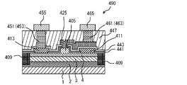
- FIG. 7 shows a plan view of the nitride semiconductor device 410 of the modified example of the second embodiment
- FIG. 8 shows a cross-sectional view of the PN diode 490 which is a component thereof.
- a protection diode 492 configured by connecting a PN diode 490 in series is inserted between the gate and source of the nitride semiconductor device 310 in the second embodiment.
- the protection diode 492 is manufactured and integrated on the same chip as the FET by the same manufacturing process as the FET.
- a buffer layer 2 composed of an AlN layer and an AlGaN layer, a GaN channel layer 3, and an AlGaN barrier layer 4 are formed as a semiconductor laminate structure by epitaxial growth on a Si substrate 1.
- a p-type GaN layer 405 that has been epitaxially grown and then etched is formed.
- a high-concentration two-dimensional electron gas (not shown) is formed due to the effects of piezoelectric polarization and spontaneous polarization.
- the region in which the resistance of the two-dimensional electron gas is increased by ion implantation is the device separation region 409.
- a SiN film 441 is formed on the surfaces of the AlGaN barrier layer 4 and the p-type GaN layer 405 as a surface protective film, and the SiN film 441 is opened to form a dummy electrode 411 and a cathode electrode 413. Further, a SiO film is formed as the first dielectric film 443 on the SiN film 441.
- the anode electrode 425 is formed on the p-type GaN layer 405 by opening the SiN film 441 and the first dielectric film 443. The anode electrode 425 extends above the dummy electrode 411.
- a SiO film which is a second dielectric film 447, is formed on the anode electrode 425 and the cathode electrode 413.
- a via 451 on the cathode electrode 413 and a via 461 on the anode electrode 425 are formed by a conventional photolithography technique and a technique for dry etching the second dielectric film 447 and the first dielectric film 443.
- plugs 453 and 463 for filling the respective vias are formed. W (tungsten) is used for the portions of the plugs 453 and 463 in contact with the second dielectric film 447, with the TiN film as a barrier layer.
- the plug 453 is connected to the cathode electrode lead-out wire 455, and the plug 463 is connected to the anode lead-out wire 465.
- FIG. 7 shows a nitride semiconductor device 410 in which a protection diode 492 is electrically inserted between the source and gate.
- the protection diode 492 has five PN diodes 490 shown in FIG. 8 connected in series. Each PN diode 490 is formed in a second active region 498 surrounded by a device separation region 409 that is highly resistant by ion implantation. Further, the five PN diodes 490 are electrically connected in series by the anode-cathode wiring 483.
- the protection diode 492 is connected to the first source lead-out wire 355 by the anode-source wire 481 and is connected to the first gate lead-out wire 365 or the gate pad 393 by the cathode-gate wire 485.
- the dielectric breakdown voltage of the SiO film is about 3 MV / cm, and the dielectric breakdown voltage when the thickness of the SiO film (not shown) between the source electrode 311 and the gate electrode connecting portion 325 in FIG. 7 is 0.1 ⁇ m. Is 30V.
- the rising voltage of the GaN PN diode is about 3.5V. Since five PN diodes 490 are connected in series to the protection diode 492 of the nitride semiconductor device 310 in the present embodiment, a current flows when a reverse bias of about 17.5 V is applied between the source and the gate. That is, with a sufficient voltage margin, the dielectric breakdown between the gate electrode connecting portion 325 and the source electrode 311 is not dielectrically broken, and the source gate of the nitride semiconductor device 410 is protected.
- the area of the element separation region 409 is increased by the protection diode 492 as compared with the nitride semiconductor device 310, and as a result, the chip area is slightly increased.
- the protection diode 492 can be designed to have a smaller area than the FET which is a power transistor, the increase in the chip area is small.
- the number of PN diodes connected in series is 5, but the quantity is appropriately designed, for example, 3 to 10 depending on the required protection voltage. It is possible to do.
- the ratio of the first active region 408 to the chip area is smaller than that in the nitride semiconductor device 310 in the second embodiment, but it is sufficient as compared with the case where the POE technique is not used. Is big. As a result, the on-resistance is small and the chip area is small.
- the diode semiconductor device has a second active region surrounded by an element separation region on the substrate, and is formed in the second active region.
- a protection diode is formed in which a plurality of these diodes are connected in series, the anode of the protection diode is electrically connected to the source electrode, and the cathode of the protection diode is electrically connected to the gate electrode connection portion.
- the rising voltage of the current flowing from the anode to the cathode of the protection diode is lower than the insulation breakdown voltage of the first dielectric film.
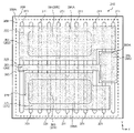
- FIG. 3 is plan views showing the nitride semiconductor device 510 according to the third embodiment of the present disclosure.
- 10 is an enlarged view of the dotted line portion M in FIG. 9, and
- FIG. 11 is an enlarged view of the dotted line portion N in FIG.
- the wiring layer is omitted in order to explain the portion of the FET under the wiring layer.
- FIG. 11 has the same configuration as that of the first embodiment.
- the first gate electrode 521 and the second gate electrode 523 are each coupled by a gate electrode connecting portion 525 at the central portion thereof.
- the gate electrode connecting portion 525 is formed of the same metal layer as the first gate electrode 521 and the second gate electrode 523 at the same time. Therefore, the number of manufacturing processes does not increase.
- the gate electrode connecting portion 525 is a SiO film which is a first dielectric film. It is formed on (not shown) and is electrically isolated from the source electrode 511.
- the width of the gate electrode connecting portion 525 is about 3 ⁇ m, and the length is designed to be larger than that of the first gate electrode 521 and the second gate electrode 523, which are about 1 ⁇ m in length. This design allows for the back end of line using vias and plugs described below, which is difficult on gate electrodes.
- a SiO film (not shown), which is a second dielectric film, is placed on the first gate electrode 521, the second gate electrode 523, the gate electrode connecting portion 525, the source electrode 511, and the drain electrodes 531 and 533. It is formed.
- the SiO film is designed to have a thickness that prevents dielectric breakdown between the source and drain. For example, in a 600V withstand voltage transistor, the thickness of the SiO film is 2 ⁇ m to 3 ⁇ m.
- the via 551 on the source electrode 511 can be obtained by ordinary photolithography technology and dry etching technology for the SiO film.
- Vias 561 on the gate electrode connecting portion 525 and vias 571 on the drain electrodes 531 and 533 are formed.
- plugs 553, 563, and 573 that fill the respective vias are formed.
- W tungsten
- the plug 555 is connected to the first source lead-out wire 555
- the plug 563 is connected to the first gate lead-out wire 565
- the plug 573 is connected to the first drain lead-out wire 575.
- a SiO film (not shown) is formed as a third dielectric film on the first source lead-out wiring 555, the first gate lead-out wiring 565, and the first drain lead-out wiring 575. Similar to the above, by the photolithography technique and the technique of dry etching the third dielectric film, the via 581 on the first source lead wire, the via 583 on the first gate lead wire, and the first drain lead wire are used. The upper via 585 is formed.
- plugs 582, 584, and 586 for filling the respective vias are formed.
- W tungsten
- the plug 582 is connected to the second source lead-out wire 587
- the plug 584 is connected to the second gate lead-out wire 588
- the plug 586 is connected to the second drain lead-out wire 589.
- the first source lead-out wiring 555 is sandwiched between the first gate lead-out wiring 565, and the drain lead-out wiring 575 is sandwiched between the first gate lead-out wiring 565.
- the gate wiring resistance is lowered, and at the same time, the drain lead-out wiring 575 to which a high voltage is applied is not arranged at the chip end, so that the reliability regarding moisture resistance is improved.
- the distance W2 between the first drain outlet wiring 575 and the first gate outlet wiring 565 is larger than the distance W1 between the first source outlet wiring 555 and the first gate outlet wiring 565.
- the second gate lead-out wiring 588 extends in the Y direction to form a gate pad 593 having a large area at its end.
- the gate pad 593 has a gate pad opening 593A formed with respect to a surface protective film (not shown) of the nitride semiconductor device 510.
- the second source lead-out wiring 587 extends in the Y direction, and the vicinity of the central portion thereof serves as a source pad 591.
- the source pad 591 has a source pad opening 591A formed with respect to a surface protective film (not shown) of the nitride semiconductor device 510.
- the second drain lead-out wiring 589 extends in the Y direction and becomes a drain pad 595 in the vicinity of the central portion thereof.
- the drain pad 595 has a drain pad opening 595A formed with respect to a surface protective film (not shown) of the nitride semiconductor device 510.
- the first active region 508, the device separation region 509, and the boundary 508A of the ion implantation region, which is the boundary between the two, are provided.
- the nitride semiconductor device 510 since the ratio of the first active region 508 to the chip area is high, the on-resistance is small and the chip area is small.
- the second gate lead-out wiring 588, the second source lead-out wiring 587, and the second drain lead-out wiring 589 are formed of the same metal layer. Therefore, the manufacturing process becomes simple.
- the same metal layer are Al (aluminum), Cu (copper), and Au (gold).
- Cu aluminum
- Cu copper
- Au gold
- each pad is formed by using only one wiring layer, but in the present embodiment, two wiring layers are used.
- each of the source / drain gates is compared with the case where only one wiring layer is used.
- Wiring resistance can be lowered.
- the wiring resistance of the gate uses two wiring layers, it is possible to significantly reduce the wiring resistance as compared with the examples of Cited Document 2 and the like. Further, since it is not necessary to form the gate wiring in the element separation region 509, the chip area is also reduced.
- the first gate lead-out wiring, the first source lead-out wiring, and the first drain lead-out wiring, and the first gate lead-out wiring is described.
- a third dielectric film is formed on the wiring, the first source lead-out wiring, and the first drain lead-out wiring, and a plurality of the said firsts are formed through vias formed on the third dielectric film.
- the second gate lead-out wiring extending in the second direction by electrically connecting the gate lead-out wiring of 1 and the plurality of the first source lead-out wirings are electrically connected in the second direction. It has a second source outlet wiring to be extended and a second drain outlet wiring to electrically connect a plurality of the first drain extraction wirings and extend in the second direction.
- the resistance of each lead-out wiring of the source / drain gate can be lowered as compared with the case where the wiring layer is one layer.
- the two wiring layers of the first gate lead-out wiring and the second gate lead-out wiring are used, there is an effect that the wiring resistance of the gate can be reduced.
- it is not necessary to form the gate lead-out wiring in the element separation region there is an effect that the chip area can be reduced.
- both sides of the first source lead-out wiring may be sandwiched by the first gate lead-out wiring, and the first drain lead-out wiring may be sandwiched by the first gate lead-out wiring.
- the drain lead-out wiring to which a high voltage is applied is not arranged at the chip end, so that the reliability regarding moisture resistance can be improved.
- the distance between the first drain withdrawal wiring and the first gate withdrawal wiring may be larger than the distance between the first source withdrawal wiring and the first gate withdrawal wiring.
- the electric field in the vicinity of the first drain lead-out wiring to which a high voltage is applied can be weakened, and the reliability regarding moisture resistance can be improved.
- the second gate lead-out wiring, the second source lead-out wiring, and the second drain lead-out wiring may be formed of the same metal wiring layer.
- the manufacturing process for forming the second gate lead-out wiring, the second source lead-out wiring, and the second drain lead-out wiring can be simplified.
- FIGS. 13A, 13B, 13C, and 13D are XIIIa-XIIIa line, XIIIb-XIIIb line, XIIIc-XIIIc line, and XIIId- in FIG. A cross-sectional view of the XIIId line is shown.
- the present embodiment is a double gate transistor having two gates.
- a buffer layer 2 composed of an AlN layer and an AlGaN layer, a GaN channel layer 3, and an AlGaN barrier layer 4 are formed as a semiconductor laminate structure on a Si substrate 1 by epitaxial growth. It is formed.
- p-type GaN layers 605, 606, 607, and 608 that have been epitaxially grown and then etched are formed.
- a high-concentration two-dimensional electron gas (not shown) is formed due to the effects of piezoelectric polarization and spontaneous polarization.
- the region where the two-dimensional electron gas is formed is the active region 609 of FIG. 12, and the region where the two-dimensional electron gas is made highly resistant by ion implantation is the device separation region 610.
- the boundary between the two is the boundary 609A of the ion implantation region.
- the element separation region 610 may be formed by removing the region containing the two-dimensional electron gas by mesa etching.
- a SiN film 641 is formed on the surfaces of the AlGaN barrier layer 4 and the p-type GaN layers 605, 606, 607, and 608 as surface protective films, and the SiN film 641 is formed.
- the first source electrode 631 and the second source electrode 633 are formed by opening.
- a SiO film is formed on the SiN film 641 as the first dielectric film 643.
- the SiN film 641 and the first dielectric film 643 are opened so that the first gate electrode 621, the second gate electrode 622, the third gate electrode 625, and the fourth gate electrode 626 are the p-type GaN layer 605. It is formed on 606, 607, and 608, respectively.
- the first gate electrode 621 and the second gate electrode 622 are formed at positions on both sides separated from each other in the X direction with respect to the finger-shaped first source electrode 631. Further, the third gate electrode 625 and the fourth gate electrode 626 are formed at positions on both sides separated from the finger-shaped second source electrode 633 in the X direction.
- first gate electrode 621 and the second gate electrode 622 are finger-shaped in the Y direction, which is a direction perpendicular to the X direction, together with the p-type GaN layer 605 and the p-type GaN layer 606 at the lower portions thereof. It is stretched and connected in an arc shape at both ends. With this configuration, the leakage current flowing between the first source electrode 631 and the second source electrode 633 in the off state is reduced.
- the finger-shaped gate electrode needs to reach the device separation region 610 beyond the boundary 609A of the ion implantation region. The same applies to the third gate electrode 625 and the fourth gate electrode 626.
- the first gate electrode 621 and the second gate electrode 622 are each coupled by the first gate electrode connecting portion 623 near the center thereof.
- the first gate electrode connecting portion 623 is formed of the same metal layer as the first gate electrode 621 and the second gate electrode 622 at the same time. Therefore, the number of manufacturing processes does not increase.
- the first gate electrode connecting portion 623 is the first dielectric. It is formed on the SiO film which is the body film 643, and is electrically insulated from the first source electrode 631.
- the width (depth direction of the paper surface) of the first gate electrode connecting portion 623 is about 3 ⁇ m, which is designed to be larger than the first gate electrode 621 and the second gate electrode 622 having a length of about 1 ⁇ m. .. This design allows for the back end of line using vias and plugs described below, which is difficult on gate electrodes.
- the third gate electrode 625 and the fourth gate electrode 626 are each coupled by a second gate electrode connecting portion 627 near the center thereof.
- SiO film which is a second dielectric film 647, is formed on the electrodes 631 and the second source electrode 633.
- the second dielectric film 647 is designed to have a thickness that prevents dielectric breakdown between the first source and the second source in the double gate transistor for high withstand voltage. For example, in the 600V withstand voltage double gate transistor, when the second dielectric film 647 is SiO, the thickness thereof is set to 2 ⁇ m to 3 ⁇ m.
- the width of the first source electrode 631, the first gate electrode connecting portion 623, the second gate electrode connecting portion 627, and the second source electrode 633 is about 3 ⁇ m
- the normal photolithography technique and the first Via 681 on the first source electrode 631, via 671 on the first gate electrode connecting portion 623, and the second source electrode by the technique of dry etching the dielectric film 647 of 2 and the first dielectric film 643.
- a via 651 on 633 and a via 661 on a second gate electrode connecting portion 627 are formed.
- plugs 683, 673, 653, and 663 that fill the respective vias are formed.
- W tungsten
- the plug 683 is connected to the lead wire 685 of the first source electrode
- the plug 673 is connected to the lead wire 675 of the first gate electrode
- the plug 653 is connected to the lead wire 655 of the second source electrode
- the plug 663 is connected. Is connected to the lead-out wiring 665 of the second gate electrode.
- the first gate electrode 621 and the second gate electrode 622 are connected by the first gate electrode connecting portion 623 at the central portion. Then, a via 671 is formed in the first gate electrode connecting portion 623 to perform gate wiring. Further, the third gate electrode 625 and the fourth gate electrode 626 are connected by a second gate electrode connecting portion 627 at the central portion. Then, a via 671 is formed in the first gate electrode connecting portion 623 and a via 661 is formed in the second gate electrode connecting portion 627 to perform gate wiring. Therefore, the gate wiring resistance is significantly reduced as compared with the case where the gate wiring is performed from the end of the gate electrode. Further, the gate wiring is formed not on the element separation region 610 but on the active region 609. As a result, the chip area does not increase.
- the side surface where the first source electrode 631 and the second source electrode 633 are in contact with the first dielectric film 643 has a cross section.
- the shape may be a forward taper. Due to the shape of the forward taper, the coverage with respect to the side surfaces of the first source electrode 631 and the second source electrode 633 of the first dielectric film 643 is improved, and voids (voids) and seams (seam) are not generated. As a result, a reverse bias voltage of several tens of volts was applied between the first source electrode 631 and the first gate electrode connecting portion 623, and between the second source electrode 633 and the second gate electrode connecting portion 627. Even in this case, there is an effect that the first dielectric film 643 is unlikely to undergo dielectric breakdown.
- a low resistance metal layer serving as a field plate electrode is placed on the first source electrode 631 and the second source electrode 633. May be provided.
- the configuration of FIG. 12 is repeatedly formed in the X direction, and the first source pad is formed in the lead-out wiring 685 of the first source electrode.
- the second source and the second are A protection diode may be inserted between the gates.
- the first source pad, the second source pad, the first gate pad, and the first source pad are used by using the wiring technique of the second layer as in the third embodiment. 2 gate pads may be formed.
- the nitride semiconductor device has a substrate, a semiconductor laminated structure composed of a plurality of nitride semiconductor layers on the substrate, and an element separation region around the upper surface side of the semiconductor laminated structure.
- a first active region surrounded by, and a first source electrode located on both sides of the first active region separated from the first source electrode in the first direction in a plan view.
- the first gate electrode, the second gate electrode, the second source electrode, the third gate electrode and the fourth gate electrode located on both sides of the second source electrode separated in the first direction in a plan view.
- the first source electrode, the first gate electrode, the second gate electrode, the second source electrode, the third gate electrode, and the fourth gate electrode have a gate electrode.
- the finger-shaped portion has a finger-shaped portion extending in a second direction perpendicular to the first direction in a plan view, and a first dielectric film is formed on the first source electrode and the second source electrode.
- the first gate electrode and the second gate electrode are electrically connected by a first gate electrode connecting portion formed on the first dielectric film, and the third gate is formed.
- the electrode and the fourth gate electrode are electrically connected by a second gate electrode connecting portion formed on the first dielectric film.
- the wiring length can be shortened and the wiring resistance of the gate can be reduced.
- the wiring resistance of the gate can be reduced.
- the first gate electrode, the second gate electrode, the first gate electrode connecting portion, the third gate electrode, the fourth gate electrode, and the second gate electrode connecting portion are the same. It may be formed of the metal layer of.
- the first gate electrode, the second gate electrode, the first gate electrode connecting portion, the third gate electrode, the fourth gate electrode, and the second gate electrode connecting portion It has the effect of not increasing the manufacturing process.
- the width of the first gate electrode connecting portion is larger than the length of the first gate electrode and the length of the second gate electrode, and the width of the second gate electrode connecting portion is the width of the third gate. It may be larger than the electrode length and the fourth gate electrode length.
- the portion in contact with the first dielectric film has a forward taper shape
- the portion in contact with the first dielectric film is formed. It may have a forward taper shape.
- the coverage of the first dielectric film with respect to the side surfaces of the first and second source electrodes is improved, and the generation of voids (voids) and seams (seam) is suppressed.
- a reverse bias voltage for example, several tens of volts
- the present disclosure is not limited to this embodiment. As long as it does not deviate from the gist of the present disclosure, various modifications that can be conceived by those skilled in the art are applied to this embodiment, and a form constructed by combining components in different embodiments is also within the scope of one or more embodiments. May be included within.
- the nitride semiconductor device in the nitride semiconductor device according to the present disclosure, it can be used as a switching transistor having a low gate wiring resistance.
Landscapes
- Engineering & Computer Science (AREA)
- Microelectronics & Electronic Packaging (AREA)
- Power Engineering (AREA)
- Physics & Mathematics (AREA)
- Condensed Matter Physics & Semiconductors (AREA)
- General Physics & Mathematics (AREA)
- Computer Hardware Design (AREA)
- Ceramic Engineering (AREA)
- Junction Field-Effect Transistors (AREA)
Abstract
窒化物半導体装置は、素子分離領域(9)で囲まれる第1の活性領域(8)と、第1の活性領域(8)の上にソース電極(11)、ソース電極(11)に対して平面視で第1方向に離間した両側に位置する第1のゲート電極(21)と第2のゲート電極(23)、第1のゲート電極(21)または第2のゲート電極(23)に対してソース電極(11)と反対方向に位置する少なくとも1つのドレイン電極(31/33)を有し、ソース電極(11)、第1のゲート電極(21)、第2のゲート電極(23)、及びドレイン電極(31/33)は、平面視で第1方向と垂直な第2方向に延伸するフィンガー状の部分を有し、ソース電極(11)の上には第1の誘電体膜(43)が形成されており、第1のゲート電極(21)と第2のゲート電極(23)は、第1の誘電体膜(43)の上に形成されたゲート電極連結部(25)によって、電気的に接続している。
Description
本開示は、半導体材料として窒化ガリウム(GaN)等の窒化物半導体を用いた窒化物半導体装置に関する。
近年、スイッチング用のパワートランジスタとして窒化物半導体であるGaNを用いた電界効果トランジスタ(GaN-FET)の商品化が進んでいる。GaN-FETとしては、半導体基板上にGaN層をチャネル層、AlGaNをバリア層として形成して、これらの2つの層で形成されるヘテロ接合界面に自発分極とピエゾ分極で発生する2次元電子ガスをチャネルとして用いる構造が一般的である。
このような構造のGaN-FETにおいては、基板と平行方向にチャネル電流が流れることになる。その結果、FETにワイヤボンディング等を通して外部から電圧を供給したり電流を流したりする、ソースパッド、ドレインパッド、ゲートパッドは、いずれも基板の表面側に形成される。従って、チップ面積削減によってGaN-FETのコストを下げるためには、チップ面積全体に占めるパッド面積を削減することが重要となってくる。
このようなパッド面積の削減のために、FETが実際にトランジスタ動作をしている領域(活性領域)の上に各パッドを形成するPOE(Pad on Element)またはPOA(Pad over Active)と呼ばれる技術が開発されている(特許文献1、特許文献2)。この技術を用いることで、パッドによるチップ面積の増大は発生しないため、チップ面積削減には極めて有効である。
しかしながら、従来の窒化物半導体装置におけるPOEを実現する配線技術においては、ゲート電極の配線は、活性領域の外側の素子分離領域に形成されていた。特許文献2の段落0038においても、「ゲート電極8は活性領域の外側で束ねられ、さらに活性領域の外周を迂回してゲート電極パッド層23と接続されている。」と記載されている通りである。その結果、大出力化のためにパワートランジスタに含まれる単位トランジスタの数量を多くするにつれ、ゲートパッドに到達するまでのゲート電極の配線長が長くなるという課題がある。その場合は、ゲート配線抵抗が大きくなることにより、高速のスイッチングが行えなくなる。すなわち、ゲート電極の配線技術に関して改善の余地がある。
本開示は上記課題に鑑み、ゲート電極の配線を活性領域の上で行うことにより、ゲート電極パッドまでの配線長が短くなる結果、ゲートの配線抵抗が低くなり、高速スイッチング動作に適した窒化物半導体装置を提供することを主な目的とする。
その他の課題と新規な特徴は、本明細書の記述および添付図面から明らかにする。
上記課題を解決するために、本開示の一態様に係る窒化物半導体装置においては、基板と、前記基板の上に複数の窒化物半導体層からなる半導体積層構造と、前記半導体積層構造の上面側に、周囲を素子分離領域で囲まれる第1の活性領域と、前記第1の活性領域の上にソース電極、前記ソース電極に対して平面視で第1方向に離間した両側に位置する第1のゲート電極と第2のゲート電極、前記第1のゲート電極または前記第2のゲート電極に対して前記ソース電極と反対方向に位置する少なくとも1つのドレイン電極を有し、前記ソース電極、前記第1のゲート電極、前記第2のゲート電極、及び前記ドレイン電極は、平面視で前記第1方向と垂直な第2方向に延伸するフィンガー状の部分を有し、前記ソース電極の上には第1の誘電体膜が形成されており、前記第1のゲート電極と前記第2のゲート電極は、前記第1の誘電体膜の上に形成されたゲート電極連結部によって、電気的に接続している。
また、上記課題を解決するために、本開示の他の一形態に係る窒化物半導体装置においては、基板と、前記基板の上に複数の窒化物半導体層からなる半導体積層構造と、前記半導体積層構造の上面側に、周囲を素子分離領域で囲まれる第1の活性領域と、前記第1の活性領域の上に、第1のソース電極と、前記第1のソース電極に対して平面視で第1方向に離間した両側に位置する第1のゲート電極と第2のゲート電極と、第2のソース電極と、前記第2のソース電極に対して平面視で第1方向に離間した両側に位置する第3のゲート電極と第4のゲート電極とを有し、前記第1のソース電極、前記第1のゲート電極、前記第2のゲート電極、前記第2のソース電極、前記第3のゲート電極、前記第4のゲート電極は、平面視で前記第1方向と垂直な第2方向に延伸するフィンガー状の部分を有し、前記第1のソース電極と前記第2のソース電極の上には第1の誘電体膜が形成されており、前記第1のゲート電極と前記第2のゲート電極は、前記第1の誘電体膜の上に形成された第1のゲート電極連結部によって電気的に接続し、前記第3のゲート電極と前記第4のゲート電極は、前記第1の誘電体膜の上に形成された第2のゲート電極連結部によって電気的に接続している。
本開示により、ゲート配線抵抗を低くできる窒化物半導体装置を提供する。
以下、実施の形態について、図面を参照して詳細に説明する。なお、以下で説明する実施の形態は、いずれも包括的または具体的な例を示すものである。以下の実施の形態で示される数値、形状、材料、構成要素、構成要素の配置位置及び接続形態などは、一例であり、本開示を限定する主旨ではない。また、本開示の実現形態は、現行の独立請求項に限定されるものではなく、他の独立請求項によっても表現され得る。
(実施形態1)
図1は実施形態1の窒化物半導体装置10の平面図を、図2A、図2B、図2Cは図1における、IIa-IIa線、IIb-IIb線、IIc-IIc線の断面図をそれぞれ示す。
図1は実施形態1の窒化物半導体装置10の平面図を、図2A、図2B、図2Cは図1における、IIa-IIa線、IIb-IIb線、IIc-IIc線の断面図をそれぞれ示す。
図2A、図2B、図2Cに示すように、Si基板1上にAlN層やAlGaN層からなるバッファー層2、GaNチャネル層3、AlGaNバリア層4が半導体積層体構造として、エピタキシャル成長により形成されている。AlGaNバリア層4の上には、AlGaNバリア層4にエピタキシャル成長された後にエッチング加工されたp型GaN層5とp型GaN層6とが形成されている。GaNチャネル層3、AlGaNバリア層4の界面においては、ピエゾ分極と自発分極の効果により高濃度の2次元電子ガスが形成されている。この2次元電子ガスが形成されている領域が図1に示す第1の活性領域8であり、2次元電子ガスがイオン注入により高抵抗化された領域が素子分離領域9である。そして、第1の活性領域8と素子分離領域9の境界が、イオン注入領域の境界8Aである。なお素子分離領域9は、メサエッチングにより、2次元電子ガスを含む領域を除去して形成しても良い。
図2A、図2B、図2Cに示すように、AlGaNバリア層4とp型GaN層5とp型GaN層6の表面は表面保護膜としてSiN膜41が形成され、SiN膜41を開口してソース電極11、ドレイン電極31とドレイン電極33が形成されている。さらに、SiN膜41の上には第1の誘電体膜43としてSiO膜が形成されている。p型GaN層5とp型GaN層6の上のSiN膜41と第1の誘電体膜43を開口して、第1のゲート電極21と第2のゲート電極23が、それぞれ形成されている。
図1に示すように、第1のゲート電極21と第2のゲート電極23は、フィンガー状のソース電極11に対して平面視で第1方向に離間した両側の位置に形成されている。ここで、第1方向は、図1ではX方向である。さらに、フィンガー状のドレイン電極31は、第1のゲート電極21に対してソース電極11と反対方向に位置し、フィンガー状のドレイン電極33は、第2のゲート電極23に対してソース電極11と反対方向に位置する。また、第1のゲート電極21と第2のゲート電極23は、それぞれの下部にあるp型GaN層5とp型GaN層6とともに、平面視で第1方向に垂直な方向である第2方向にフィンガー状となって延伸し、両端部で円弧状となって繋がっている。ここで、第2方向は、図1ではY方向である。この構成により、オフ状態においてソース電極11とドレイン電極31とドレイン電極33の間に流れるリーク電流が低減する。なお、第1のゲート電極21と第2のゲート電極23を端部で繋がない場合は、フィンガー状のゲート電極はイオン注入領域の境界8Aを超えて、素子分離領域9に到達する必要がある。
図2Bに示すように、第1のゲート電極21と第2のゲート電極23はそれぞれ、その中央部においてゲート電極連結部25によって結合している。このゲート電極連結部25は、第1のゲート電極21と第2のゲート電極23と同一の金属層で、同時に形成される。そのため、製造工程数の増加は発生しない。ただし、第1のゲート電極21と第2のゲート電極23はp型GaN層5とp型GaN層6にそれぞれ接触しているのに対し、ゲート電極連結部25は第1の誘電体膜43であるSiO膜の上に形成され、ソース電極11とは電気的に絶縁している。また、ゲート電極連結部25の幅(紙面の奥行方向)は3μm程度で、いずれも長さが1μm程度である第1のゲート電極21と第2のゲート電極23よりも大きく設計されている。この設計により、ゲート電極上では困難である、この後に説明するビアとプラグを用いる配線工程が可能となる。
図2A、図2B、図2Cに示すように、第1のゲート電極21、第2のゲート電極23、ゲート電極連結部25、ソース電極11、ドレイン電極31とドレイン電極33の上には、第2の誘電体膜47であるSiO膜が形成される。第2の誘電体膜47は高耐圧用トランジスタにおいては、ソース・ドレイン間の絶縁破壊を防ぐ厚さに設計する。例えば600V耐圧用トランジスタにおいては、第2の誘電体膜47をSiO膜とした場合には、その厚さを2μmから3μmとする。この場合、ソース電極11、ゲート電極連結部25、ドレイン電極31の幅をいずれも3μm程度とすれば、通常のフォトリソグラフィー技術と第2の誘電体膜47及び第1の誘電体膜43をドライエッチングする技術により、ソース電極11上のビア51、ゲート電極連結部25上のビア61、ドレイン電極31とドレイン電極33上のビア71が形成される。そして、それぞれのビアを充填するプラグ53、63、73が形成されている。プラグ53、63、73は第2の誘電体膜47と接する部分はTiN膜をバリア層として、W(タングステン)が用いられる。プラグ53は第1のソース引き出し配線55と接続し、プラグ63は第1のゲート引き出し配線65に接続し、プラグ73は第1のドレイン引き出し配線75に接続している。
本実施形態においては、第1のゲート電極21と第2のゲート電極23の中央部においてゲート電極連結部25で接続されている。そして、ゲート電極連結部25にビア61を形成してゲート配線が行われている。従って、ゲート電極の端部からゲート配線を行う場合に比べて、ゲート配線抵抗が大幅に減少する。ゲート配線抵抗の低下によって窒化物半導体装置10は、高速スイッチング動作に適している。
また、ゲート配線は素子分離領域9の上ではなく、第1の活性領域8の上で形成される。その結果、チップ面積の増大も発生しない。さらに、ソース電極11とゲート電極連結部25との間には、第1の誘電体膜43による容量が発生する。この容量はゲート・ソース間容量となるが、スイッチング用のパワートランジスタにおいて誤点弧を防ぐためには、ゲート・ドレイン間容量に対して、ゲート・ソース間容量を増やすことが望ましい。従って、本実施形態を用いることで、ゲート・ソース間容量が大きく誤点弧を防ぐことが可能なスイッチング用のパワートランジスタを実現することができる。
なお、本実施形態における窒化物半導体装置10ではビアを充填するプラグとしてWを用いたが、Al(アルミニウム)やCu(銅)を用いても良い。Cuを用いる場合は、デュアルダマシン法を使って、プラグとそれに接続する配線を同時に形成しても良い。
なお、図1においては、ゲート電極連結部25の上のビア61は1個としているが、製造技術の点から可能であれば複数個形成しても構わない。また、ソース電極11やドレイン電極31と33の上のビア71の数は、配線抵抗を減らすために多い方が良いが、ビアとプラグを形成する製造技術の点から適宜設計される。
以上のように実施形態1に係る窒化物半導体装置は、基板と、前記基板の上に複数の窒化物半導体層からなる半導体積層構造と、前記半導体積層構造の上面側に、周囲を素子分離領域で囲まれる第1の活性領域と、前記第1の活性領域の上にソース電極、前記ソース電極に対して平面視で第1方向に離間した両側に位置する第1のゲート電極と第2のゲート電極、前記第1のゲート電極または前記第2のゲート電極に対して前記ソース電極と反対方向に位置する少なくとも1つのドレイン電極を有し、前記ソース電極、前記第1のゲート電極、前記第2のゲート電極、及び前記ドレイン電極は、平面視で前記第1方向と垂直な第2方向に延伸するフィンガー状の部分を有し、前記ソース電極の上には第1の誘電体膜が形成されており、前記第1のゲート電極と前記第2のゲート電極は、前記第1の誘電体膜の上に形成されたゲート電極連結部によって、電気的に接続している。
これによれば、ゲート電極の配線(この配線はフィンガー状の部分を含む)を、平面視において第1の活性領域の外側ではなく内側に形成することにより、配線長を短くし、ゲートの配線抵抗を低減することができる。その結果、スイッチング動作の高速化に適しているという効果がある。また、ゲート電極の配線を、平面視において活性領域の内側に形成することにより、窒化物半導体装置としてのチップの面積を縮小できるという効果がある。
例えば、前記第1のゲート電極、前記第2のゲート電極、および前記ゲート電極連結部は、同一の金属層で形成されもよい。
これによれば、ゲート電極連結部によりゲート電極の配線抵抗を低下させることができる。しかも第1のゲート電極、第2のゲート電極およびゲート電極連結部の形成において、製造工程を増加させないという効果がある。
例えば、前記ゲート電極連結部の幅は、前記第1のゲート電極長及び前記第2のゲート電極長よりも大きくてもよい。
これによれば、ゲート電極連結部に対してビアとプラグを用いる配線が可能にし、チップ面積を縮小することができる。
(実施形態1の変形例1)
図3は実施形態1の変形例を示す窒化物半導体装置110の部分的な断面図であり、実施形態1の図2Bのソース電極11近傍に対応する部分を拡大した図である。ドレイン電極、ビア、プラグ、配線等は省略している。図3に示すように、AlGaNバリア層4とp型GaN層105と106の表面は表面保護膜としてSiN膜141が形成され、SiN膜141を開口してソース電極111が形成されている。さらに、SiN膜141の上には第1の誘電体膜143としてSiO膜が形成されている。SiN膜141と第1の誘電体膜143を開口して第1のゲート電極121と第2のゲート電極123が、p型GaN層105と106の上にそれぞれ形成されている。そして、第1のゲート電極121と第2のゲート電極123がゲート電極連結部125により結合している。
図3は実施形態1の変形例を示す窒化物半導体装置110の部分的な断面図であり、実施形態1の図2Bのソース電極11近傍に対応する部分を拡大した図である。ドレイン電極、ビア、プラグ、配線等は省略している。図3に示すように、AlGaNバリア層4とp型GaN層105と106の表面は表面保護膜としてSiN膜141が形成され、SiN膜141を開口してソース電極111が形成されている。さらに、SiN膜141の上には第1の誘電体膜143としてSiO膜が形成されている。SiN膜141と第1の誘電体膜143を開口して第1のゲート電極121と第2のゲート電極123が、p型GaN層105と106の上にそれぞれ形成されている。そして、第1のゲート電極121と第2のゲート電極123がゲート電極連結部125により結合している。
本変形例においては、ソース電極111が第1の誘電体膜143と接する側面は断面形状が順テーパーとなっている。順テーパーの角度としては、45°以上で75°以下が好ましく、50°以上で70°以下が更に好ましい。この形状により、第1の誘電体膜143のソース電極111の側面に対するカバレージが良くなり、ボイド(空隙)やシーム(継ぎ目)が発生しなくなる。その結果、ソース電極111とゲート電極連結部125の間に数10Vの逆バイアス電圧が印加された場合においても、第1の誘電体膜143が絶縁破壊することが起きにくいという効果がある。
本変形例のける順テーパーの断面形状を実現するには、ドライエッチングのエッチングマスクとなるレジストを熱処理により断面形状に順テーパーをつけること等により実現できる。
以上のように実施形態1の変形例1に係る窒化物半導体装置は、前記ソース電極の側面において、前記第1の誘電体膜と接する部分は順テーパー形状である。
これによれば、第1の誘電体膜のソース電極の側面に対するカバレージが良くなり、ボイド(空隙)やシーム(継ぎ目)が発生を抑制する。その結果、ソース電極とゲート電極連結部の間に逆バイアス電圧(例えば数10V)が印加された場合においても、第1の誘電体膜が絶縁破壊することが起きにくいという効果がある。
(実施形態1の変形例2)
図4は実施形態1の変形例2の窒化物半導体装置210の平面図を、図5A、図5B、図5Cは図4におけるVa-Va線、Vb-Vb線、Vc-Vc線の断面図をそれぞれ示す。
図4は実施形態1の変形例2の窒化物半導体装置210の平面図を、図5A、図5B、図5Cは図4におけるVa-Va線、Vb-Vb線、Vc-Vc線の断面図をそれぞれ示す。
図5A、図5B、図5Cに示すように、Si基板1上にAlN層やAlGaN層からなるバッファー層2、GaNチャネル層3、AlGaNバリア層4が半導体積層体構造として、エピタキシャル成長により形成されている。AlGaNバリア層4の上には、エピタキシャル成長された後にエッチング加工されたp型GaN層5とp型GaN層6が形成されている。GaNチャネル層3、AlGaNバリア層4の界面においては、ピエゾ分極と自発分極の効果により高濃度の2次元電子ガス(図示せず)が形成されている。この2次元電子ガスが形成されている領域が図4の第1の活性領域208であり、2次元電子ガスがイオン注入により高抵抗化された領域が素子分離領域209である。そして、第1の活性領域208と素子分離領域209の境界が、イオン注入領域の境界208Aである。なお素子分離領域209は、メサエッチングにより、2次元電子ガスを含む領域を除去して形成しても良い。
図5A、図5B、図5Cに示すように、AlGaNバリア層4とp型GaN層5とp型GaN層6の表面は表面保護膜としてSiN膜241が形成され、SiN膜241を開口してソース電極211、ドレイン電極231と233が形成されている。さらに、SiN膜241の上には第1の誘電体膜243としてSiO膜が形成されている。SiN膜241と第1の誘電体膜243を開口して第1のゲート電極221と第2のゲート電極223が、p型GaN層5とp型GaN層6の上にそれぞれ形成されている。
図4に示すように、第1のゲート電極221と第2のゲート電極223は、フィンガー状のソース電極211に対してX方向に離間した両側の位置に形成されている。さらに、フィンガー状のドレイン電極231は、第1のゲート電極221に対してソース電極211と反対方向に位置し、フィンガー状のドレイン電極233は、第2のゲート電極223に対してソース電極211と反対方向に位置する。
また、第1のゲート電極221と第2のゲート電極223は、それぞれの下部にあるp型GaN層5とp型GaN層6とともに、X方向に垂直な方向であるY方向にフィンガー状となって延伸し、両端部で円弧状となって繋がっている。この構成により、オフ状態においてソース電極211とドレイン電極231、233の間に流れるリーク電流が低減する。なお、第1のゲート電極221と第2のゲート電極223を端部で繋がない場合は、フィンガー状のゲート電極はイオン注入領域の境界208Aを超えて、素子分離領域209に到達する必要がある。
図5Bに示すように、第1のゲート電極221と第2のゲート電極223は、それぞれの中央部においてゲート電極連結部225によって結合している。このゲート電極連結部225は、第1のゲート電極221と第2のゲート電極223と同一の金属層で、同時に形成されている。そのため、製造工程数の増加は発生しない。ただし、第1のゲート電極221と第2のゲート電極223はp型GaN層5とp型GaN層6にそれぞれ接触しているのに対し、ゲート電極連結部225は第1の誘電体膜243の上に形成され、ソース電極211とは電気的に絶縁している。また、ゲート電極連結部225の幅(紙面の奥行方向)は3μm程度で、いずれも長さが1μm程度である第1のゲート電極221と第2のゲート電極223よりも大きく設計されている。この設計により、ゲート電極上では困難である、この後に説明するビアとプラグを用いる配線工程が可能となる。
図5A、図5B、図5Cに示すように、第1のゲート電極221、第2のゲート電極223、ソース電極211、ドレイン電極231、233を覆うフィールドプレート膜としてSiO膜245を形成する。図5Aと図5Cに示すように、ソース電極211上に、SiO膜245と第1の誘電体膜243を開口して、ソースフィールドプレート電極となる低抵抗金属層285を形成する。低抵抗金属層285はp型GaN層5とp型GaN層6のドレイン側の端部での電界集中を緩和させる効果をもたらす。その結果、耐圧が向上するとともに、窒化物半導体装置で課題となる電流コラプスという現象も緩和する。さらに、この低抵抗金属層285はゲート電極連結部225の近傍以外のソース電極211の上に形成されるので、ソース電極211の配線抵抗を下げる効果もある。
同様に、図5A、図5B、図5Cに示すように、ドレイン電極231とドレイン電極233の上に、SiO膜245と第1の誘電体膜243を開口して、低抵抗金属層281と低抵抗金属層283をそれぞれ形成する。この低抵抗金属層281と低抵抗金属層283は、図4に示すように、ドレイン電極231とドレイン電極233の上に全面的に形成されるので、ドレイン電極231とドレイン電極233の配線抵抗を下げる効果がある。
また、図5Bに示すように、ゲート電極連結部225の上に、SiO膜245を開口して、低抵抗金属層287を形成することで、ゲートの配線抵抗も下がるという効果がある。
低抵抗金属層281、283、285、287の上には、第2の誘電体膜247であるSiO膜が形成される。第2の誘電体膜247は高耐圧用トランジスタにおいては、ソース・ドレイン間の絶縁破壊を防ぐ厚さに設計する。例えば600V耐圧用トランジスタにおいては、第2の誘電体膜247をSiO膜とした場合には、そのの厚さを2μmから3μmとする。この場合、低抵抗金属層281、283、285、287における最も短い寸法においても3μm程度以上とすれば、通常のフォトリソグラフィー技術と第2の誘電体膜247をドライエッチングする技術により、低抵抗金属層285上のビア251、低抵抗金属層287上のビア261、低抵抗金属層281と283上のビア271が形成される。そして、それぞれのビアを充填するプラグ253、263、273が形成されている。プラグ253、263、273は第2の誘電体膜247と接する部分はTiN膜をバリア層として、W(タングステン)が用いられる。プラグ253は第1のソース引き出し配線255と接続し、プラグ263は第1のゲート引き出し配線265に接続し、プラグ273は第1のドレイン引き出し配線275に接続している。
本実施形態においては、第1のゲート電極221と第2のゲート電極223の中央部においてゲート電極連結部225で接続されている。そして、ゲート電極連結部225にビア261を形成してゲート配線が行われている。従って、ゲート電極の端部からゲート配線を行う場合に比べて、ゲート配線抵抗が大幅に減少する。また、ゲート配線は素子分離領域209の上ではなく、第1の活性領域208の上で形成される。その結果、チップ面積の増大も発生しない。さらに、ソース電極211とゲート電極連結部225との間には、第1の誘電体膜243による容量が発生する。この容量はゲート・ソース間容量となるが、スイッチング用のパワートランジスタにおいて誤点弧を防ぐためには、ゲート・ドレイン間容量に対して、ゲート・ソース間容量を増やすことが望ましい。従って、本実施形態を用いることで、ゲート・ソース間容量が大きく誤点弧を防ぐことが可能なスイッチング用のパワートランジスタを実現することができる。
なお、本実施形態における窒化物半導体装置210ではビアを充填するプラグとしてWを用いたが、Al(アルミニウム)やCu(銅)を用いても良い。Cuを用いる場合は、デュアルダマシン法を使って、プラグとそれに接続する配線を同時に形成しても良い。
なお、図4においては、ゲート電極連結部225の上の低抵抗金属層287の上にあるビア261は1個としているが、製造技術の点から可能であれば複数個形成しても構わない。また、ソース電極211やドレイン電極231と233の上のビア271の数は、配線抵抗を減らすために多い方が良いが、ビアとプラグを形成する製造技術の点から適宜設計される。
以上のように実施形態1の変形例2に係る窒化物半導体装置は、前記ゲート電極連結部の下部を除いた前記ソース電極の上と、前記ドレイン電極の上には低抵抗金属層が形成されている。
これによれば、低抵抗金属層はソース電極の上に形成されるのでソース電極の配線抵抗を下げる効果がある。また、低抵抗金属層はドレイン電極の上に形成されるので、ドレイン電極の配線抵抗を下げる効果がある。
例えば、前記ソース電極の上に形成された前記低抵抗金属層は、前記第1のゲート電極および前記第2のゲート電極の上方を超えて、前記ドレイン電極の方向に延伸するソースフィールドプレート電極であってもよい。
これによれば、低抵抗金属層はゲートのドレイン側端部での電界集中を緩和させる効果がある。その結果、耐圧が向上するとともに、電流コラプスという現象も緩和する効果がある。
(実施形態2)
実施形態2の窒化物半導体装置310の平面図を図6に示す。
実施形態2の窒化物半導体装置310の平面図を図6に示す。
本実施形態は、実施形態1またはその変形例1、変形例2の窒化物半導体装置を図6に示すX方向に繰り返して配置して、パワートランジスタを構成するものである。図6においては、簡略化のために本実施形態を説明する上で特に必要のない構成要素は省略している。
図6に示すように、いずれもY方向にフィンガー状となって延伸するソース電極311とドレイン電極331が、X方向に交互に複数個配置されている。X方向の両端は、高電圧が印加されるドレイン電極331ではなく、グランド接地される場合が多いソース電極311であることにより、外部からの水分浸入を防ぐ効果があり信頼性の点で優れている。複数のソース電極311の上に形成されたゲート電極連結部325はその上に形成された誘電体膜(図示せず)に開口されたビア361があり、ビア361を充填するようにプラグ363がある。各プラグ363を繋ぐように第1のゲート引き出し配線365が形成されている。第1のゲート引き出し配線365はその端部において面積が広いゲートパッド393となっている。ゲートパッド393は窒化物半導体装置310の表面保護膜(図示せず)に対してゲートパッド開口部393Aが形成されている。
複数のソース電極311はその上に形成された誘電体膜(図示せず)に開口されたビア351があり、ビア351を充填するようにプラグ353がある。各プラグ353を繋ぐように第1のソース引き出し配線355が形成されている。第1のソース引き出し配線355はその中央部においてソースパッド391となっている。ソースパッド391は表面保護膜(図示せず)に対してソースパッド開口部391Aが形成されている。
複数のドレイン電極331はその上に形成された誘電体膜(図示せず)に開口されたビア371があり、ビア371を充填するようにプラグ373がある。各プラグ373を繋ぐように第1のドレイン引き出し配線375が形成されている。第1のドレイン引き出し配線375はその中央部においてドレインパッド395となっている。ドレインパッド395は表面保護膜(図示せず)に対してドレインパッド開口部395Aが形成されている。
本実施形態においては、第1のソース引き出し配線355と第1のドレイン引き出し配線375は、第1のゲート引き出し配線365を挟んで形成されている。第1のゲート引き出し配線365がゲート電極連結部325を介して各ゲート電極(図示せず)に接続しているのでゲート配線抵抗が低く、第1の活性領域308の上部に形成されているので、チップ面積の増加もない。
本実施形態においては、第1のゲート引き出し配線365、第1のソース引き出し配線355、第1のドレイン引き出し配線375は、同一の金属層で形成される。そのために製造工程は簡略なものになる。同一の金属層の例としてはAl(アルミニウム)、Cu(銅)、Au(金)である。特にCuを用いた場合、デュアルダマシン法を用いればプラグ363、353、373と同時に形成することが可能となり、さらに製造工程は簡略なものとなる。
本実施形態においては、第1の活性領域308と素子分離領域309、そして、両者の境界であるイオン注入領域の境界308Aを有す。窒化物半導体装置310はチップ面積に対する第1の活性領域308の割合が高くなるために、オン抵抗が小さくチップ面積が小さくなる。
以上のように実施形態2に係る窒化物半導体装置において、前記第1方向に、前記ソース電極、前記第1のゲート電極、前記第2のゲート電極、前記ゲート電極連結部、前記ドレイン電極が繰り返して形成され、複数の前記ゲート電極連結部の上には第2の誘電体膜が形成され、前記第2の誘電体膜に形成されたビアを介して、複数の前記ゲート電極連結部を電気的に接続して、前記第1方向に延伸する第1のゲート引き出し配線を有する。
これによれば、高速スイッチング動作において電力供給用の大電流を制御できるという効果がある。また、第1のソース引き出し配線と第1のドレイン引き出し配線は、第1のゲート引き出し配線365を挟んで形成されるので、チップ面積の縮小できるという効果がある。
例えば、前記第2の誘電体膜は、前記ソース電極、前記第1のゲート電極、前記第2のゲート電極、前記ドレイン電極の上にも形成され、前記第1のゲート引き出し配線を挟んで、前記第2の誘電体膜に形成されたビアを介して複数の前記ソース電極を電気的に接続して、前記第1方向に延伸する第1のソース引き出し配線と、前記第2の誘電体膜に形成されたビアを介して複数の前記ドレイン電極を電気的に接続して、前記第1方向に延伸する第1のドレイン引き出し配線とを有してもよい。
これによれば、窒化物半導体装置のチップ面積に対する第1の活性領域の割合を高くできるために、オン抵抗を小さくし、かつ、チップ面積を小さくすることという効果がある。
例えば、前記第1のゲート引き出し配線、前記第1のソース引き出し配線、前記第1のドレイン引き出し配線は同一の金属配線層で形成されてもよい。
これによれば、第1のゲート引き出し配線、第1のソース引き出し配線、第1のドレイン引き出し配線の形成において製造工程を簡略にできるという効果がある。
例えば、前記第1のゲート引き出し配線の一部に形成されたゲートパッドと、前記第1のソース引き出し配線の一部に形成されたソースパッドと、前記第1のドレイン引き出し配線の一部に形成されたドレインパッドとを有していてもよい。
これによれば、第1の活性領域の上にゲートパッド、ソースパッド、ドレインパッドを形成するPOE(Pad on Element)またはPOA(Pad over Active)を実現するので、パッドによるチップ面積の増大は抑制し、または、チップ面積を削減するという効果がある。
(実施形態2の変形例)
実施形態2の変形例の窒化物半導体装置410の平面図を図7に、その構成要素であるPNダイオード490の断面図を図8に示す。本変形例は、実施形態2における窒化物半導体装置310のゲート・ソース間に、PNダイオード490の直列接続により構成される保護ダイオード492が、挿入された構成である。この保護ダイオード492はFETと同じチップ上に、FETと同じ製造工程により作られて集積化される。
実施形態2の変形例の窒化物半導体装置410の平面図を図7に、その構成要素であるPNダイオード490の断面図を図8に示す。本変形例は、実施形態2における窒化物半導体装置310のゲート・ソース間に、PNダイオード490の直列接続により構成される保護ダイオード492が、挿入された構成である。この保護ダイオード492はFETと同じチップ上に、FETと同じ製造工程により作られて集積化される。
図8に示すように、Si基板1上にAlN層やAlGaN層からなるバッファー層2、GaNチャネル層3、AlGaNバリア層4が半導体積層体構造として、エピタキシャル成長により形成されている。AlGaNバリア層4の上には、エピタキシャル成長された後にエッチング加工されたp型GaN層405が形成されている。GaNチャネル層3、AlGaNバリア層4の界面においては、ピエゾ分極と自発分極の効果により高濃度の2次元電子ガス(図示せず)が形成されている。2次元電子ガスがイオン注入により高抵抗化された領域が素子分離領域409である。
AlGaNバリア層4とp型GaN層405の表面は表面保護膜としてSiN膜441が形成され、SiN膜441を開口してダミー電極411、カソード電極413が形成されている。さらに、SiN膜441の上には第1の誘電体膜443としてSiO膜が形成されている。SiN膜441と第1の誘電体膜443を開口してアノード電極425が、p型GaN層405の上に形成されている。てアノード電極425はダミー電極411の上にまで延長されている。
アノード電極425、カソード電極413の上には、第2の誘電体膜447であるSiO膜が形成される。通常のフォトリソグラフィー技術と第2の誘電体膜447及び第1の誘電体膜443をドライエッチングする技術により、カソード電極413の上のビア451、アノード電極425上のビア461が形成される。そして、それぞれのビアを充填するプラグ453、463が形成されている。プラグ453、463は第2の誘電体膜447と接する部分はTiN膜をバリア層として、W(タングステン)が用いられる。プラグ453はカソード電極引き出し配線455と接続し、プラグ463はアノード引き出し配線465に接続している。
図7は、保護ダイオード492を、電気的にソース・ゲート間に入れた窒化物半導体装置410を示している。保護ダイオード492は、図8で示したPNダイオード490が5個、直列に接続されている。各PNダイオード490は、周囲をイオン注入で高抵抗された素子分離領域409に囲まれた第2の活性領域498の中に形成されている。また、5個のPNダイオード490は、アノード・カソード間配線483により、電気的に直列に接続されている。保護ダイオード492はアノード・ソース間配線481により第1のソース引き出し配線355に接続して、カソード・ゲート間配線485により、第1のゲート引き出し配線365、またはゲートパッド393に接続する。
SiO膜の絶縁破壊電圧は3MV/cm程度であり、図7におけるソース電極311とゲート電極連結部325の間のSiO膜(図示せず)の厚さを0.1μmとした場合に絶縁破壊電圧は30Vとなる。一方、GaNのPNダイオードの立ち上がり電圧は約3.5Vである。本実施形態における窒化物半導体装置310の保護ダイオード492には、PNダイオード490を5個直列にしているので、ソース・ゲート間に約17.5Vの逆バイアスが印加された場合に電流が流れる。すなわち、十分な電圧マージンを持って、ゲート電極連結部325とソース電極311の間の誘電体膜が絶縁破壊することなく、窒化物半導体装置410のソース・ゲート間が保護される。
また図7に示すように、窒化物半導体装置410では、保護ダイオード492により素子分離領域409の面積が、窒化物半導体装置310に比べて増える結果、チップ面積がやや増える。しかしながら、保護ダイオード492はパワートランジスタであるFETに比べて面積を小さく設計できるために、チップ面積の増大はわずかである。
なお、本実施形態における窒化物半導体装置410では、直列に接続するPNダイオードの数を5個としたが、必要な保護電圧に応じて、例えば3個から10個のように数量は適宜、設計することが可能である。
本実施形態における窒化物半導体装置410においては、チップ面積に対する第1の活性領域408の割合は、実施形態2における窒化物半導体装置310よりは小さくなるが、POE技術を使わない場合に比べると十分に大きい。その結果、オン抵抗が小さくチップ面積が小さくなる。
以上のように実施形態2の変形例1に係る窒化物半導体装置は、前記基板の上に、周囲を素子分離領域で囲まれる第2の活性領域を有し、前記第2の活性領域に形成されたダイオードが複数個、直列接続された保護ダイオードが形成され、前記保護ダイオードのアノードは前記ソース電極に電気的に接続され、前記保護ダイオードのカソードは前記ゲート電極連結部に電気的に接続され、前記保護ダイオードの前記アノードから前記カソードへ流れる電流の立ち上がり電圧は、前記第1の誘電体膜の絶縁破壊電圧よりも低い。
これによれば、ゲート電極連結部とソース電極の間の誘電体膜が絶縁破壊することを抑制し、窒化物半導体装置の信頼性を向上させるという効果がある。
(実施形態3)
図9、図10、図11は本開示における第3の実施形態を窒化物半導体装置510示す平面図である。図9の点線部Mの拡大図が図10、図10の点線部Nの拡大図が図11である。図11においては、配線層の下層にあるFETの部分を説明するために、配線層は省略してある。
図9、図10、図11は本開示における第3の実施形態を窒化物半導体装置510示す平面図である。図9の点線部Mの拡大図が図10、図10の点線部Nの拡大図が図11である。図11においては、配線層の下層にあるFETの部分を説明するために、配線層は省略してある。
図11は、実施形態1と同様な構成である。第1のゲート電極521と第2のゲート電極523はそれぞれ、その中央部においてゲート電極連結部525によって結合している。このゲート電極連結部525は、第1のゲート電極521と第2のゲート電極523と同一の金属層で、同時に形成される。そのため、製造工程数の増加は発生しない。ただし、第1のゲート電極521と第2のゲート電極523はp型GaN層(図示せず)に接触しているのに対し、ゲート電極連結部525は第1の誘電体膜であるSiO膜(図示せず)の上に形成され、ソース電極511とは電気的に絶縁している。また、ゲート電極連結部525の幅は3μm程度で、長さが1μm程度である第1のゲート電極521と第2のゲート電極523よりも大きく設計されている。この設計により、ゲート電極上では困難である、以下に説明するビアとプラグを用いる配線工程が可能となる。
第1のゲート電極521、第2のゲート電極523、ゲート電極連結部525、ソース電極511、ドレイン電極531と533の上には、第2の誘電体膜であるSiO膜(図示せず)が形成される。SiO膜は高耐圧用トランジスタにおいては、ソース・ドレイン間の絶縁破壊を防ぐ厚さに設計する。例えば600V耐圧用トランジスタにおいては、SiO膜の厚さを2μmから3μmとする。この場合、ソース電極511、ゲート電極連結部525、ドレイン電極531と533の幅を3μm程度とすれば、通常のフォトリソグラフィー技術とSiO膜をドライエッチングする技術により、ソース電極511上のビア551、ゲート電極連結部525上のビア561、ドレイン電極531と533上のビア571が形成される。そして、それぞれのビアを充填するプラグ553、563、573が形成されている。プラグ553、563、573はSiO膜と接する部分はTiN膜をバリア層として、W(タングステン)が用いられる。
図10に示すように、プラグ553は第1のソース引き出し配線555と接続し、プラグ563は第1のゲート引き出し配線565に接続し、プラグ573は第1のドレイン引き出し配線575に接続している。第1のソース引き出し配線555、第1のゲート引き出し配線565、第1のドレイン引き出し配線575の上には、第3の誘電体膜としてSiO膜(図示せず)が形成される。上記と同様に、フォトリソグラフィー技術と第3の誘電体膜をドライエッチングする技術により、第1のソース引き出し配線上のビア581、第1のゲート引き出し配線上のビア583、第1のドレイン引き出し配線上のビア585が形成される。そして、それぞれのビアを充填するプラグ582、584、586が形成されている。プラグ582、584、586はSiO膜と接する部分はTiN膜をバリア層として、W(タングステン)が用いられる。プラグ582は第2のソース引き出し配線587と接続し、プラグ584は第2のゲート引き出し配線588に接続し、プラグ586は第2のドレイン引き出し配線589に接続している。
図10において、第1のソース引き出し配線555は、第1のゲート引き出し配線565に挟まれ、ドレイン引き出し配線575は、第1のゲート引き出し配線565に挟まれている。この結果、ゲート配線抵抗が下がると同時に、高電圧が印加されるドレイン引き出し配線575がチップ端に配置されないために、耐湿性に関する信頼性が向上する。
さらに図10において、第1のドレイン引き出し配線575と第1のゲート引き出し配線565の間隔W2は、第1のソース引き出し配線555と第1のゲート引き出し配線565の間隔W1よりも大きい。この結果、高電圧が印加される第1のドレイン引き出し配線575の近傍における電界が弱くなり、耐湿性に関する信頼性が向上する。
図9に示すように、第2のゲート引き出し配線588はY方向に延伸して、その端部において面積が広いゲートパッド593となっている。ゲートパッド593は窒化物半導体装置510の表面保護膜(図示せず)に対してゲートパッド開口部593Aが形成されている。また、第2のソース引き出し配線587はY方向に延伸して、その中央部付近がソースパッド591となっている。ソースパッド591は窒化物半導体装置510の表面保護膜(図示せず)に対してソースパッド開口部591Aが形成されている。同様に、第2のドレイン引き出し配線589はY方向に延伸して、その中央部付近においてドレインパッド595となっている。ドレインパッド595は窒化物半導体装置510の表面保護膜(図示せず)に対してドレインパッド開口部595Aが形成されている。
本実施形態においては、第1の活性領域508と素子分離領域509、そして、両者の境界であるイオン注入領域の境界508Aを有す。窒化物半導体装置510はチップ面積に対する第1の活性領域508の割合が高くなるために、オン抵抗が小さくチップ面積が小さくなる。
本実施形態においては、第2のゲート引き出し配線588、第2のソース引き出し配線587、第2のドレイン引き出し配線589は、同一の金属層で形成される。そのために製造工程は簡略なものになる。同一の金属層の例としてはAl(アルミニウム)、Cu(銅)、Au(金)である。特にCuを用いた場合、デュアルダマシン法を用いればプラグ582、584、586と同時に形成することが可能となり、さらに製造工程は簡略なものとなる。
実施形態2や実施形態2の変形例においては、配線層が1層のみで各パッドが形成されているが、本実施形態においては、配線層を2層用いている。この結果、ソース・ドレインのフィンガー長が長くなった場合や、ソース・ドレインのフィンガー本数が多くなった場合においても、配線層を1層しか用いない場合に比べて、ソース・ドレイン・ゲートの各配線抵抗を低くすることができる。特にゲートの配線抵抗は2層の配線層を用いるので、引用文献2等の実施例に比べて大幅に下げることが可能となる。さらに、ゲート配線を素子分離領域509に形成する必要が無いので、チップ面積も小さくなる。
なお、本実施形態においても、実施形態2の変形例のように、ソース・ゲート間に保護ダイオードを入れることも可能である。
以上のように実施形態3に係る窒化物半導体装置において、前記第1のゲート引き出し配線、前記第1のソース引き出し配線、前記第1のドレイン引き出し配線はいずれも複数あり、前記第1のゲート引き出し配線、前記第1のソース引き出し配線、前記第1のドレイン引き出し配線の上に第3の誘電体膜が形成され、前記第3の誘電体膜に形成されたビアを介して、複数の前記第1のゲート引き出し配線を電気的に接続して、前記第2方向に延伸する第2のゲート引き出し配線と、複数の前記第1のソース引き出し配線を電気的に接続して、前記第2方向に延伸する第2のソース引き出し配線と、複数の前記第1のドレイン引き出し配線を電気的に接続して、前記第2方向に延伸する第2のドレイン引き出し配線とを有する。
これによれば、ビアを介して接続される配線層を2層用いるので、配線層を1層である場合に比べて、ソース・ドレイン・ゲートの各引き出し配線の抵抗を低くすることができる。特に、第1のゲート引き出し配線および第2のゲート引き出し配線による2層の配線層を用いるので、ゲートの配線抵抗を小さくできるという効果がある。さらに、ゲート引き出し配線を素子分離領域に形成する必要が無いので、チップ面積の縮小できるという効果がある。
例えば、前記第1のソース引き出し配線の両側は前記第1のゲート引き出し配線で挟まれ、前記第1のドレイン引き出し配線は前記第1のゲート引き出し配線で挟まれていてもよい。
これによれば、ゲート配線抵抗が低下すると同時に、高電圧が印加されるドレイン引き出し配線がチップ端に配置されないために、耐湿性に関する信頼性を向上させることができる。
例えば、前記第1のドレイン引き出し配線と前記第1のゲート引き出し配線の間隔は、前記第1のソース引き出し配線と前記第1のゲート引き出し配線の間隔よりも大きくてもよい。
これによれば、高電圧が印加される第1のドレイン引き出し配線の近傍における電界を弱くし、耐湿性に関する信頼性を向上させることができる。
例えば、前記第2のゲート引き出し配線、前記第2のソース引き出し配線、前記第2のドレイン引き出し配線は同一の金属配線層で形成されてもよい。
これによれば、第2のゲート引き出し配線、第2のソース引き出し配線、および第2のドレイン引き出し配線を形成するための製造工程を簡略にすることができる。
例えば、前記第2のゲート引き出し配線の一部に形成されたゲートパッドと、前記第2のソース引き出し配線の一部に形成されたソースパッドと、前記第2のドレイン引き出し配線の一部に形成されたドレインパッドとを有していてもよい。
これによれば、2層のPOEを実現するのでチップ面積を大きく縮小できるという効果がある。
(実施形態4)
図12は実施形態4の窒化物半導体装置620の平面図を、図13A、図13B、図13C、図13Dは、図12におけるXIIIa-XIIIa線、XIIIb-XIIIb線、XIIIc-XIIIc線、XIIId-XIIId線、の断面図をそれぞれ示す。本実施形態はゲートを2つ有するダブルゲートトランジスタである。
図12は実施形態4の窒化物半導体装置620の平面図を、図13A、図13B、図13C、図13Dは、図12におけるXIIIa-XIIIa線、XIIIb-XIIIb線、XIIIc-XIIIc線、XIIId-XIIId線、の断面図をそれぞれ示す。本実施形態はゲートを2つ有するダブルゲートトランジスタである。
図13A、図13B、図13C、図13Dに示すように、Si基板1上にAlN層やAlGaN層からなるバッファー層2、GaNチャネル層3、AlGaNバリア層4が半導体積層体構造として、エピタキシャル成長により形成されている。AlGaNバリア層4の上には、エピタキシャル成長された後にエッチング加工されたp型GaN層605、606、607、608が形成されている。GaNチャネル層3、AlGaNバリア層4の界面においては、ピエゾ分極と自発分極の効果により高濃度の2次元電子ガス(図示せず)が形成されている。この2次元電子ガスが形成されている領域が図12の活性領域609であり、2次元電子ガスがイオン注入により高抵抗化された領域が素子分離領域610である。両者の境界がイオン注入領域の境界609Aである。なお素子分離領域610は、メサエッチングにより、2次元電子ガスを含む領域を除去して形成しても良い。
図13A、図13B、図13C、図13Dに示すように、AlGaNバリア層4とp型GaN層605、606、607、608の表面は表面保護膜としてSiN膜641が形成され、SiN膜641を開口して第1のソース電極631、第2のソース電極633が形成されている。さらに、SiN膜641の上には第1の誘電体膜643としてSiO膜が形成されている。SiN膜641と第1の誘電体膜643を開口して第1のゲート電極621、第2のゲート電極622、第3のゲート電極625、第4のゲート電極626が、p型GaN層605、606、607、608の上にそれぞれ形成されている。
図12に示すように、第1のゲート電極621と第2のゲート電極622は、フィンガー状の第1のソース電極631に対してX方向に離間した両側の位置に形成されている。また、第3のゲート電極625と第4のゲート電極626は、フィンガー状の第2のソース電極633とX方向に対して離間した両側の位置に形成されている。
また、第1のゲート電極621と第2のゲート電極622は、それぞれの下部にあるp型GaN層605とp型GaN層606とともに、X方向に垂直な方向であるY方向にフィンガー状となって延伸し、両端部で円弧状となって繋がっている。この構成により、オフ状態において第1のソース電極631と第2のソース電極633の間に流れるリーク電流が低減する。第1のゲート電極621と第2のゲート電極622を端部で繋がない場合は、フィンガー状のゲート電極はイオン注入領域の境界609Aを超えて素子分離領域610に到達する必要がある。第3のゲート電極625と第4のゲート電極626に関しても同様である。
図13Cに示すように、第1のゲート電極621と第2のゲート電極622はそれぞれ、その中央付近において第1のゲート電極連結部623によって結合している。この第1のゲート電極連結部623は、第1のゲート電極621と第2のゲート電極622と同一の金属層で、同時に形成される。そのため、製造工程数の増加は発生しない。ただし、第1のゲート電極621と第2のゲート電極622はp型GaN層605とp型GaN層606にそれぞれ接触しているのに対し、第1のゲート電極連結部623は第1の誘電体膜643であるSiO膜の上に形成され、第1のソース電極631とは電気的に絶縁している。また、第1のゲート電極連結部623の幅(紙面の奥行方向)は3μm程度で、長さが1μm程度である第1のゲート電極621と第2のゲート電極622よりも大きく設計されている。この設計により、ゲート電極上では困難である、以下に説明するビアとプラグを用いる配線工程が可能となる。同様に、図13Bに示すように、第3のゲート電極625と第4のゲート電極626はそれぞれ、その中央付近において第2のゲート電極連結部627によって結合している。
第1のゲート電極621、第2のゲート電極622、第1のゲート電極連結部623、第3のゲート電極625、第4のゲート電極626、第2のゲート電極連結部627、第1のソース電極631、第2のソース電極633の上には、第2の誘電体膜647であるSiO膜が形成される。第2の誘電体膜647は高耐圧用のダブルゲートトランジスタにおいては、第1ソース・第2ソース間の絶縁破壊を防ぐ厚さに設計する。例えば600V耐圧用ダブルゲートトランジスタにおいては、第2の誘電体膜647をSiOとした場合に、その厚さを2μmから3μmとする。この場合、第1のソース電極631、第1のゲート電極連結部623、第2のゲート電極連結部627、第2のソース電極633の幅を3μm程度とすれば、通常のフォトリソグラフィー技術と第2の誘電体膜647及び第1の誘電体膜643をドライエッチングする技術により、第1のソース電極631上のビア681、第1のゲート電極連結部623上のビア671、第2のソース電極633上のビア651、第2のゲート電極連結部627上のビア661が形成される。そして、それぞれのビアを充填するプラグ683、673、653、663が形成されている。プラグ683、673、653、663は第2の誘電体膜647と接する部分はTiN膜をバリア層として、W(タングステン)が用いられる。プラグ683は第1のソース電極の引き出し配線685と接続し、プラグ673は第1のゲート電極の引き出し配線675と接続し、プラグ653は第2のソース電極の引き出し配線655と接続し、プラグ663は第2のゲート電極の引き出し配線665と接続している。
本実施形態においては、第1のゲート電極621と第2のゲート電極622の中央部において第1のゲート電極連結部623で接続されている。そして、第1のゲート電極連結部623にビア671を形成してゲート配線を行う。また、第3のゲート電極625と第4のゲート電極626の中央部において第2のゲート電極連結部627で接続されている。そして、第1のゲート電極連結部623にビア671を、第2のゲート電極連結部627にビア661を形成してゲート配線が行われている。従って、ゲート電極の端部からゲート配線を行う場合に比べて、ゲート配線抵抗が大幅に減少する。また、ゲート配線は素子分離領域610の上ではなく、活性領域609の上で形成される。その結果、チップ面積の増大も発生しない。
なお本実施形態の窒化物半導体装置620においては、実施形態1の変形例1のように、第1のソース電極631と第2のソース電極633が第1の誘電体膜643と接する側面は断面形状が順テーパーとなっていても良い。順テーパーの形状により、第1の誘電体膜643の第1のソース電極631と第2のソース電極633の側面に対するカバレージが良くなり、ボイド(空隙)やシーム(継ぎ目)が発生しなくなる。その結果、第1のソース電極631と第1のゲート電極連結部623の間や、第2のソース電極633と第2のゲート電極連結部627の間に数10Vの逆バイアス電圧が印加された場合においても、第1の誘電体膜643が絶縁破壊することが起きにくいという効果がある。
なお本実施形態の窒化物半導体装置620においては、実施形態1の変形例2のように、第1のソース電極631と第2のソース電極633の上に、フィールドプレート電極となる低抵抗金属層が設けられていても良い。
なお本実施形態の窒化物半導体装置620においては、実施形態2のように、図12の構成がX方向に繰り返し形成され、第1のソース電極の引き出し配線685の中に第1のソースパッド、第2のソース電極の引き出し配線655の中に第2のソースパッド、第1のゲート電極の引き出し配線675の中に第1のゲートパッド、第2のゲート電極の引き出し配線665の中に第2のゲートパッドが形成されても良い。
なお本実施形態の窒化物半導体装置620においては、実施形態2の変形例のように、第1のソースと第1のゲートの間に保護ダイオードを入れても、第2のソースと第2にゲートの間に保護ダイオードを入れても良い。
なお本実施形態の窒化物半導体装置620においては、実施形態3のように、2層目の配線技術を用いることにより、第1のソースパッド、第2のソースパッド、第1のゲートパッド、第2のゲートパッドを形成しても良い。
以上のように実施形態4に係る窒化物半導体装置は、基板と、前記基板の上に複数の窒化物半導体層からなる半導体積層構造と、前記半導体積層構造の上面側に、周囲を素子分離領域で囲まれる第1の活性領域と、前記第1の活性領域の上に、第1のソース電極と、前記第1のソース電極に対して平面視で第1方向に離間した両側に位置する第1のゲート電極と第2のゲート電極と、第2のソース電極と、前記第2のソース電極に対して平面視で第1方向に離間した両側に位置する第3のゲート電極と第4のゲート電極とを有し、前記第1のソース電極、前記第1のゲート電極、前記第2のゲート電極、前記第2のソース電極、前記第3のゲート電極、前記第4のゲート電極は、平面視で前記第1方向と垂直な第2方向に延伸するフィンガー状の部分を有し、前記第1のソース電極と前記第2のソース電極の上には第1の誘電体膜が形成されており、前記第1のゲート電極と前記第2のゲート電極は、前記第1の誘電体膜の上に形成された第1のゲート電極連結部によって電気的に接続し、前記第3のゲート電極と前記第4のゲート電極は、前記第1の誘電体膜の上に形成された第2のゲート電極連結部によって電気的に接続している。
これによれば、ゲート電極の配線を、平面視において第1の活性領域の内側に形成することにより、配線長を短くし、ゲートの配線抵抗を低減することができえる。その結果、スイッチング動作の高速化に適しているという効果がある。また、ゲート電極の配線を、平面視において活性領域の内側に形成することにより、窒化物半導体装置としてのチップの面積を縮小できるという効果がある。
例えば、前記第1のゲート電極、前記第2のゲート電極、前記第1のゲート電極連結部、前記第3のゲート電極、前記第4のゲート電極、前記第2のゲート電極連結部は、同一の金属層で形成されてもよい。
これによれば、第1のゲート電極、第2のゲート電極、第1のゲート電極連結部、第3のゲート電極、第4のゲート電極、および前記第2のゲート電極連結部の形成において、製造工程を増加させないという効果がある。
例えば、前記第1のゲート電極連結部の幅は、前記第1のゲート電極長と前記第2のゲート電極長よりも大きく、前記第2のゲート電極連結部の幅は、前記第3のゲート電極長と前記第4のゲート電極長よりも大きくてもよい。
これによれば、ゲート電極連結部に対してビアとプラグを用いる配線が可能にし、チップ面積を縮小することができる。
例えば、前記第1のソース電極の側面において、前記第1の誘電体膜と接する部分は順テーパー形状であり、前記第2のソース電極の側面において、前記第1の誘電体膜と接する部分は順テーパー形状であってもよい。
これによれば、第1の誘電体膜の第1および第2のソース電極の側面に対するカバレージが良くなり、ボイド(空隙)やシーム(継ぎ目)が発生を抑制する。その結果、ソース電極とゲート電極連結部の間に逆バイアス電圧(例えば数10V)が印加された場合においても、第1の誘電体膜が絶縁破壊することが起きにくいという効果がある。
以上、一つまたは複数の態様に係る窒化物半導体装置について、実施の形態に基づいて説明したが、本開示は、この実施の形態に限定されるものではない。本開示の趣旨を逸脱しない限り、当業者が思いつく各種変形を本実施の形態に施したものや、異なる実施の形態における構成要素を組み合わせて構築される形態も、一つまたは複数の態様の範囲内に含まれてもよい。
本開示にかかる窒化物半導体装置においては、ゲートの配線抵抗が低いスイッチング用トランジスタとして利用可能である。
1 Si基板
2 バッファー層
3 GaNチャネル層
4 AlGaNバリア層
5、6、105、106、405 p型GaN層
8、208、308、408、508 第1の活性領域
8A、208A、308A、408A、508A、609A イオン注入領域の境界
9、209、309、409、509 素子分離領域
10、110、210、310、410、510、620 半導体装置
11、111、211、311、511 ソース電極
21、121、221、521 第1のゲート電極
23、123、223、523 第2のゲート電極
25、125、225、325、525 ゲート電極連結部
31、33、231、233、331、531、533 ドレイン電極
41、141、241、441 SiN膜
43、143、243 443 第1の誘電体膜(SiO膜)
47、247、447 第2の誘電体膜(SiO膜)
51、251、351、551 ソース電極上のビア
53、253 プラグ
55、255、355、555 第1のソース引き出し配線
61、261、361、561 ゲート電極連結部上のビア
63、263 プラグ
65、265、365、565 第1のゲート引き出し配線
71、271、371、571 ドレイン電極上のビア
73、273 プラグ
75、275、375、575 第1のドレイン引き出し配線
245 SiO膜(フィールドプレート膜)
281、283、287 低抵抗金属層
285 低抵抗金属層(ソースフィールドプレート電極)
391 ソースパッド
391A ソースパッド開口部
393 ゲートパッド
393A ゲートパッド開口部
395 ドレインパッド
395A ドレインパッド開口部
405 p型層
411 ダミー電極
413 カソード電極
425 アノード電極
451 ビア
453 プラグ
455 カソード電極引き出し配線
461 ビア
463 プラグ
465 アノード電極引き出し配線
481 アノード・ソース間配線
483 アノード・カソード間配線
485 カソード・ゲート間配線
490 PNダイオード
492 保護ダイオード
498 第2の活性領域
581 第1のソース引き出し配線上のビア
582 584、586 プラグ
583 第1のゲート引き出し配線上のビア
585 第1のドレイン引き出し配線上のビア
587 第2のソース引き出し配線
588 第2のゲート引き出し配線
589 第2のドレイン引き出し配線
591 ソースパッド
591A ソースパッド開口部
593 ゲートパッド
593A ゲートパッド開口部
595 ドレインパッド
595A ドレインパッド開口
605、606、607、608 p型GaN層
609 活性領域
610 素子分離領域
621 第1のゲート電極
622 第2のゲート電極
623 第1のゲート電極連結部
625 第3のゲート電極
626 第4のゲート電極
627 第2のゲート電極連結部
631 第1のソース電極
633 第2のソース電極
641 SiN膜
643 第1の誘電体膜(SiO膜)
647 第2の誘電体膜(SiO膜)
651 第2のソース電極上のビア
653 プラグ
655 第2のソース電極の引き出し配線
661 第2のゲート電極連結部上のビア
663 プラグ
665 第2のゲート電極の引き出し配線
671 第1のゲート電極連結部上のビア
673 プラグ
675 第1のゲート電極の引き出し配線
681 第1のソース電極上のビア
683 プラグ
685 第1のソース電極の引き出し配線
Claims (20)
- 基板と、
前記基板の上に複数の窒化物半導体層からなる半導体積層構造と、
前記半導体積層構造の上面側に、周囲を素子分離領域で囲まれる第1の活性領域と、
前記第1の活性領域の上にソース電極、前記ソース電極に対して平面視で第1方向に離間した両側に位置する第1のゲート電極と第2のゲート電極、前記第1のゲート電極または前記第2のゲート電極に対して前記ソース電極と反対方向に位置する少なくとも1つのドレイン電極を有し、
前記ソース電極、前記第1のゲート電極、前記第2のゲート電極、及び前記ドレイン電極は、平面視で前記第1方向と垂直な第2方向に延伸するフィンガー状の部分を有し、
前記ソース電極の上には第1の誘電体膜が形成されており、
前記第1のゲート電極と前記第2のゲート電極は、前記第1の誘電体膜の上に形成されたゲート電極連結部によって、電気的に接続している
窒化物半導体装置。 - 前記第1のゲート電極、前記第2のゲート電極、および前記ゲート電極連結部は、同一の金属層で形成されている、
請求項1に記載の窒化物半導体装置。 - 前記ゲート電極連結部の幅は、前記第1のゲート電極長及び前記第2のゲート電極長よりも大きい、
請求項1または2に記載の窒化物半導体装置。 - 前記ソース電極の側面において、前記第1の誘電体膜と接する部分は順テーパー形状である、
請求項1から3のいずれか1項に記載の窒化物半導体装置。 - 前記基板の上に、周囲を素子分離領域で囲まれる第2の活性領域を有し、
前記第2の活性領域に形成されたダイオードが複数個、直列接続された保護ダイオードが形成され、
前記保護ダイオードのアノードは前記ソース電極に電気的に接続され、
前記保護ダイオードのカソードは前記ゲート電極連結部に電気的に接続され、
前記保護ダイオードの前記アノードから前記カソードへ流れる電流の立ち上がり電圧は、前記第1の誘電体膜の絶縁破壊電圧よりも低い、
請求項1から4のいずれか1項に記載の窒化物半導体装置。 - 前記ゲート電極連結部の下部を除いた前記ソース電極の上と、前記ドレイン電極の上には低抵抗金属層が形成されている、
請求項1から5のいずれか1項に記載の窒化物半導体装置。 - 前記ソース電極の上に形成された前記低抵抗金属層は、前記第1のゲート電極および前記第2のゲート電極の上方を超えて、前記ドレイン電極の方向に延伸するソースフィールドプレート電極である、
請求項6に記載の窒化物半導体装置。 - 前記第1方向に、前記ソース電極、前記第1のゲート電極、前記第2のゲート電極、前記ゲート電極連結部、前記ドレイン電極が繰り返して形成され、
複数の前記ゲート電極連結部の上には第2の誘電体膜が形成され、
前記第2の誘電体膜に形成されたビアを介して、複数の前記ゲート電極連結部を電気的に接続して、前記第1方向に延伸する第1のゲート引き出し配線を有する、
請求項1から7のいずれか1項に記載の窒化物半導体装置。 - 前記第2の誘電体膜は、前記ソース電極、前記第1のゲート電極、前記第2のゲート電極、前記ドレイン電極の上にも形成され、
前記第1のゲート引き出し配線を挟んで、
前記第2の誘電体膜に形成されたビアを介して複数の前記ソース電極を電気的に接続して、前記第1方向に延伸する第1のソース引き出し配線と、
前記第2の誘電体膜に形成されたビアを介して複数の前記ドレイン電極を電気的に接続して、前記第1方向に延伸する第1のドレイン引き出し配線とを有する、
請求項8に記載の窒化物半導体装置。 - 前記第1のゲート引き出し配線、前記第1のソース引き出し配線、前記第1のドレイン引き出し配線は同一の金属配線層で形成されている、
請求項9に記載の窒化物半導体装置。 - 前記第1のゲート引き出し配線の一部に形成されたゲートパッドと、
前記第1のソース引き出し配線の一部に形成されたソースパッドと、
前記第1のドレイン引き出し配線の一部に形成されたドレインパッドとを有する、
請求項9または10に記載の窒化物半導体装置。 - 前記第1のゲート引き出し配線、前記第1のソース引き出し配線、前記第1のドレイン引き出し配線はいずれも複数あり、
前記第1のゲート引き出し配線、前記第1のソース引き出し配線、前記第1のドレイン引き出し配線の上に第3の誘電体膜が形成され、
前記第3の誘電体膜に形成されたビアを介して、
複数の前記第1のゲート引き出し配線を電気的に接続して、前記第2方向に延伸する第2のゲート引き出し配線と、
複数の前記第1のソース引き出し配線を電気的に接続して、前記第2方向に延伸する第2のソース引き出し配線と、
複数の前記第1のドレイン引き出し配線を電気的に接続して、前記第2方向に延伸する第2のドレイン引き出し配線とを有する、
請求項10に記載の窒化物半導体装置。 - 前記第1のソース引き出し配線の両側は前記第1のゲート引き出し配線で挟まれ、
前記第1のドレイン引き出し配線は前記第1のゲート引き出し配線で挟まれている、
請求項12に記載の窒化物半導体装置。 - 前記第1のドレイン引き出し配線と前記第1のゲート引き出し配線の間隔は、
前記第1のソース引き出し配線と前記第1のゲート引き出し配線の間隔よりも大きい、
請求項12または13に記載の窒化物半導体装置。 - 前記第2のゲート引き出し配線、前記第2のソース引き出し配線、前記第2のドレイン引き出し配線は同一の金属配線層で形成されている、
請求項12から14のいずれか1項に記載の窒化物半導体装置。 - 前記第2のゲート引き出し配線の一部に形成されたゲートパッドと、
前記第2のソース引き出し配線の一部に形成されたソースパッドと、
前記第2のドレイン引き出し配線の一部に形成されたドレインパッドとを有する、
請求項12から15のいずれか1項に記載の窒化物半導体装置。 - 基板と、
前記基板の上に複数の窒化物半導体層からなる半導体積層構造と、
前記半導体積層構造の上面側に、周囲を素子分離領域で囲まれる第1の活性領域と、
前記第1の活性領域の上に、
第1のソース電極と、前記第1のソース電極に対して平面視で第1方向に離間した両側に位置する第1のゲート電極と第2のゲート電極と、
第2のソース電極と、前記第2のソース電極に対して平面視で第1方向に離間した両側に位置する第3のゲート電極と第4のゲート電極とを有し、
前記第1のソース電極、前記第1のゲート電極、前記第2のゲート電極、前記第2のソース電極、前記第3のゲート電極、前記第4のゲート電極は、平面視で前記第1方向と垂直な第2方向に延伸するフィンガー状の部分を有し、
前記第1のソース電極と前記第2のソース電極の上には第1の誘電体膜が形成されており、
前記第1のゲート電極と前記第2のゲート電極は、前記第1の誘電体膜の上に形成された第1のゲート電極連結部によって電気的に接続し、
前記第3のゲート電極と前記第4のゲート電極は、前記第1の誘電体膜の上に形成された第2のゲート電極連結部によって電気的に接続している
窒化物半導体装置。 - 前記第1のゲート電極、前記第2のゲート電極、前記第1のゲート電極連結部、前記第3のゲート電極、前記第4のゲート電極、および、前記第2のゲート電極連結部は、同一の金属層で形成されている、
請求項17に記載の窒化物半導体装置。 - 前記第1のゲート電極連結部の幅は、前記第1のゲート電極長と前記第2のゲート電極長よりも大きく、
前記第2のゲート電極連結部の幅は、前記第3のゲート電極長と前記第4のゲート電極長よりも大きい、
請求項17または18に記載の窒化物半導体装置。 - 前記第1のソース電極の側面において、前記第1の誘電体膜と接する部分は順テーパー形状であり、
前記第2のソース電極の側面において、前記第1の誘電体膜と接する部分は順テーパー形状である、
請求項17から19のいずれか1項に記載の窒化物半導体装置。
Priority Applications (2)
| Application Number | Priority Date | Filing Date | Title |
|---|---|---|---|
| US18/246,280 US20230361179A1 (en) | 2020-10-16 | 2021-08-16 | Nitride semiconductor device |
| JP2022556427A JPWO2022079995A1 (ja) | 2020-10-16 | 2021-08-16 |
Applications Claiming Priority (2)
| Application Number | Priority Date | Filing Date | Title |
|---|---|---|---|
| JP2020174945 | 2020-10-16 | ||
| JP2020-174945 | 2020-10-16 |
Publications (1)
| Publication Number | Publication Date |
|---|---|
| WO2022079995A1 true WO2022079995A1 (ja) | 2022-04-21 |
Family
ID=81207917
Family Applications (1)
| Application Number | Title | Priority Date | Filing Date |
|---|---|---|---|
| PCT/JP2021/029951 WO2022079995A1 (ja) | 2020-10-16 | 2021-08-16 | 窒化物半導体装置 |
Country Status (3)
| Country | Link |
|---|---|
| US (1) | US20230361179A1 (ja) |
| JP (1) | JPWO2022079995A1 (ja) |
| WO (1) | WO2022079995A1 (ja) |
Citations (6)
| Publication number | Priority date | Publication date | Assignee | Title |
|---|---|---|---|---|
| JP2009123932A (ja) * | 2007-11-15 | 2009-06-04 | Nec Corp | 半導体装置およびその製造方法 |
| JP2013058640A (ja) * | 2011-09-08 | 2013-03-28 | Toshiba Corp | 半導体装置 |
| JP2016139718A (ja) * | 2015-01-28 | 2016-08-04 | 株式会社東芝 | 半導体装置 |
| JP2018088473A (ja) * | 2016-11-29 | 2018-06-07 | 日亜化学工業株式会社 | 電界効果トランジスタ |
| JP2019512886A (ja) * | 2016-03-17 | 2019-05-16 | クリー インコーポレイテッドCree Inc. | バイパスされたゲート構造を有するトランジスタ |
| JP2020068343A (ja) * | 2018-10-26 | 2020-04-30 | 株式会社東芝 | 半導体装置 |
-
2021
- 2021-08-16 JP JP2022556427A patent/JPWO2022079995A1/ja active Pending
- 2021-08-16 WO PCT/JP2021/029951 patent/WO2022079995A1/ja active Application Filing
- 2021-08-16 US US18/246,280 patent/US20230361179A1/en active Pending
Patent Citations (6)
| Publication number | Priority date | Publication date | Assignee | Title |
|---|---|---|---|---|
| JP2009123932A (ja) * | 2007-11-15 | 2009-06-04 | Nec Corp | 半導体装置およびその製造方法 |
| JP2013058640A (ja) * | 2011-09-08 | 2013-03-28 | Toshiba Corp | 半導体装置 |
| JP2016139718A (ja) * | 2015-01-28 | 2016-08-04 | 株式会社東芝 | 半導体装置 |
| JP2019512886A (ja) * | 2016-03-17 | 2019-05-16 | クリー インコーポレイテッドCree Inc. | バイパスされたゲート構造を有するトランジスタ |
| JP2018088473A (ja) * | 2016-11-29 | 2018-06-07 | 日亜化学工業株式会社 | 電界効果トランジスタ |
| JP2020068343A (ja) * | 2018-10-26 | 2020-04-30 | 株式会社東芝 | 半導体装置 |
Also Published As
| Publication number | Publication date |
|---|---|
| US20230361179A1 (en) | 2023-11-09 |
| JPWO2022079995A1 (ja) | 2022-04-21 |
Similar Documents
| Publication | Publication Date | Title |
|---|---|---|
| US10950524B2 (en) | Heterojunction semiconductor device for reducing parasitic capacitance | |
| US8928039B2 (en) | Semiconductor device including heterojunction field effect transistor and Schottky barrier diode | |
| JP6277429B2 (ja) | 半導体装置 | |
| JP4645313B2 (ja) | 半導体装置 | |
| US11257938B2 (en) | Group III nitride semiconductor device with first and second conductive layers | |
| JP2006513580A (ja) | パワー半導体素子 | |
| JP2007150282A (ja) | 電界効果トランジスタ | |
| JP2012517699A (ja) | Iii族窒化物デバイスおよび回路 | |
| WO2016098390A1 (ja) | 電界効果トランジスタ | |
| US20240128263A1 (en) | Nitride semiconductor device | |
| US11133399B2 (en) | Semiconductor device | |
| WO2014050054A1 (ja) | 半導体装置 | |
| TW201705445A (zh) | 半導體裝置 | |
| JP6584987B2 (ja) | 半導体装置 | |
| US9035320B2 (en) | Semiconductor device | |
| JP7097708B2 (ja) | 窒化物半導体装置 | |
| CN106373996B (zh) | 半导体装置 | |
| WO2022079995A1 (ja) | 窒化物半導体装置 | |
| JP2016009774A (ja) | 半導体装置 | |
| TWI584467B (zh) | 半導體裝置 | |
| JP7476062B2 (ja) | 半導体装置 | |
| US11538779B2 (en) | Semiconductor device with electrode pad having different bonding surface heights | |
| TWI660506B (zh) | 半導體裝置 | |
| WO2023157452A1 (ja) | 窒化物半導体装置 | |
| JP7313197B2 (ja) | 半導体装置 |
Legal Events
| Date | Code | Title | Description |
|---|---|---|---|
| 121 | Ep: the epo has been informed by wipo that ep was designated in this application |
Ref document number: 21879737 Country of ref document: EP Kind code of ref document: A1 |
|
| ENP | Entry into the national phase |
Ref document number: 2022556427 Country of ref document: JP Kind code of ref document: A |
|
| NENP | Non-entry into the national phase |
Ref country code: DE |
|
| 122 | Ep: pct application non-entry in european phase |
Ref document number: 21879737 Country of ref document: EP Kind code of ref document: A1 |