WO2022058838A1 - 半導体装置、および電子機器 - Google Patents
半導体装置、および電子機器 Download PDFInfo
- Publication number
- WO2022058838A1 WO2022058838A1 PCT/IB2021/058112 IB2021058112W WO2022058838A1 WO 2022058838 A1 WO2022058838 A1 WO 2022058838A1 IB 2021058112 W IB2021058112 W IB 2021058112W WO 2022058838 A1 WO2022058838 A1 WO 2022058838A1
- Authority
- WO
- WIPO (PCT)
- Prior art keywords
- transistor
- potential
- wiring
- insulator
- gate
- Prior art date
- Legal status (The legal status is an assumption and is not a legal conclusion. Google has not performed a legal analysis and makes no representation as to the accuracy of the status listed.)
- Ceased
Links
Images


Classifications
-
- G—PHYSICS
- G11—INFORMATION STORAGE
- G11C—STATIC STORES
- G11C11/00—Digital stores characterised by the use of particular electric or magnetic storage elements; Storage elements therefor
- G11C11/54—Digital stores characterised by the use of particular electric or magnetic storage elements; Storage elements therefor using elements simulating biological cells, e.g. neuron
-
- G—PHYSICS
- G11—INFORMATION STORAGE
- G11C—STATIC STORES
- G11C11/00—Digital stores characterised by the use of particular electric or magnetic storage elements; Storage elements therefor
- G11C11/21—Digital stores characterised by the use of particular electric or magnetic storage elements; Storage elements therefor using electric elements
- G11C11/22—Digital stores characterised by the use of particular electric or magnetic storage elements; Storage elements therefor using electric elements using ferroelectric elements
- G11C11/223—Digital stores characterised by the use of particular electric or magnetic storage elements; Storage elements therefor using electric elements using ferroelectric elements using MOS with ferroelectric gate insulating film
-
- H—ELECTRICITY
- H10—SEMICONDUCTOR DEVICES; ELECTRIC SOLID-STATE DEVICES NOT OTHERWISE PROVIDED FOR
- H10B—ELECTRONIC MEMORY DEVICES
- H10B51/00—Ferroelectric RAM [FeRAM] devices comprising ferroelectric memory transistors
- H10B51/30—Ferroelectric RAM [FeRAM] devices comprising ferroelectric memory transistors characterised by the memory core region
-
- G—PHYSICS
- G06—COMPUTING OR CALCULATING; COUNTING
- G06G—ANALOGUE COMPUTERS
- G06G7/00—Devices in which the computing operation is performed by varying electric or magnetic quantities
- G06G7/48—Analogue computers for specific processes, systems or devices, e.g. simulators
- G06G7/60—Analogue computers for specific processes, systems or devices, e.g. simulators for living beings, e.g. their nervous systems ; for problems in the medical field
-
- G—PHYSICS
- G06—COMPUTING OR CALCULATING; COUNTING
- G06N—COMPUTING ARRANGEMENTS BASED ON SPECIFIC COMPUTATIONAL MODELS
- G06N3/00—Computing arrangements based on biological models
- G06N3/02—Neural networks
- G06N3/06—Physical realisation, i.e. hardware implementation of neural networks, neurons or parts of neurons
- G06N3/063—Physical realisation, i.e. hardware implementation of neural networks, neurons or parts of neurons using electronic means
-
- G—PHYSICS
- G11—INFORMATION STORAGE
- G11C—STATIC STORES
- G11C11/00—Digital stores characterised by the use of particular electric or magnetic storage elements; Storage elements therefor
- G11C11/21—Digital stores characterised by the use of particular electric or magnetic storage elements; Storage elements therefor using electric elements
- G11C11/22—Digital stores characterised by the use of particular electric or magnetic storage elements; Storage elements therefor using electric elements using ferroelectric elements
- G11C11/221—Digital stores characterised by the use of particular electric or magnetic storage elements; Storage elements therefor using electric elements using ferroelectric elements using ferroelectric capacitors
-
- G—PHYSICS
- G11—INFORMATION STORAGE
- G11C—STATIC STORES
- G11C11/00—Digital stores characterised by the use of particular electric or magnetic storage elements; Storage elements therefor
- G11C11/21—Digital stores characterised by the use of particular electric or magnetic storage elements; Storage elements therefor using electric elements
- G11C11/22—Digital stores characterised by the use of particular electric or magnetic storage elements; Storage elements therefor using electric elements using ferroelectric elements
- G11C11/225—Auxiliary circuits
- G11C11/2273—Reading or sensing circuits or methods
-
- G—PHYSICS
- G11—INFORMATION STORAGE
- G11C—STATIC STORES
- G11C11/00—Digital stores characterised by the use of particular electric or magnetic storage elements; Storage elements therefor
- G11C11/21—Digital stores characterised by the use of particular electric or magnetic storage elements; Storage elements therefor using electric elements
- G11C11/22—Digital stores characterised by the use of particular electric or magnetic storage elements; Storage elements therefor using electric elements using ferroelectric elements
- G11C11/225—Auxiliary circuits
- G11C11/2275—Writing or programming circuits or methods
-
- G—PHYSICS
- G11—INFORMATION STORAGE
- G11C—STATIC STORES
- G11C11/00—Digital stores characterised by the use of particular electric or magnetic storage elements; Storage elements therefor
- G11C11/21—Digital stores characterised by the use of particular electric or magnetic storage elements; Storage elements therefor using electric elements
- G11C11/22—Digital stores characterised by the use of particular electric or magnetic storage elements; Storage elements therefor using electric elements using ferroelectric elements
- G11C11/225—Auxiliary circuits
- G11C11/2297—Power supply circuits
-
- G—PHYSICS
- G11—INFORMATION STORAGE
- G11C—STATIC STORES
- G11C11/00—Digital stores characterised by the use of particular electric or magnetic storage elements; Storage elements therefor
- G11C11/21—Digital stores characterised by the use of particular electric or magnetic storage elements; Storage elements therefor using electric elements
- G11C11/34—Digital stores characterised by the use of particular electric or magnetic storage elements; Storage elements therefor using electric elements using semiconductor devices
- G11C11/40—Digital stores characterised by the use of particular electric or magnetic storage elements; Storage elements therefor using electric elements using semiconductor devices using transistors
- G11C11/401—Digital stores characterised by the use of particular electric or magnetic storage elements; Storage elements therefor using electric elements using semiconductor devices using transistors forming cells needing refreshing or charge regeneration, i.e. dynamic cells
- G11C11/403—Digital stores characterised by the use of particular electric or magnetic storage elements; Storage elements therefor using electric elements using semiconductor devices using transistors forming cells needing refreshing or charge regeneration, i.e. dynamic cells with charge regeneration common to a multiplicity of memory cells, i.e. external refresh
- G11C11/405—Digital stores characterised by the use of particular electric or magnetic storage elements; Storage elements therefor using electric elements using semiconductor devices using transistors forming cells needing refreshing or charge regeneration, i.e. dynamic cells with charge regeneration common to a multiplicity of memory cells, i.e. external refresh with three charge-transfer gates, e.g. MOS transistors, per cell
-
- H—ELECTRICITY
- H10—SEMICONDUCTOR DEVICES; ELECTRIC SOLID-STATE DEVICES NOT OTHERWISE PROVIDED FOR
- H10B—ELECTRONIC MEMORY DEVICES
- H10B53/00—Ferroelectric RAM [FeRAM] devices comprising ferroelectric memory capacitors
- H10B53/30—Ferroelectric RAM [FeRAM] devices comprising ferroelectric memory capacitors characterised by the memory core region
-
- H—ELECTRICITY
- H10—SEMICONDUCTOR DEVICES; ELECTRIC SOLID-STATE DEVICES NOT OTHERWISE PROVIDED FOR
- H10D—INORGANIC ELECTRIC SEMICONDUCTOR DEVICES
- H10D30/00—Field-effect transistors [FET]
- H10D30/60—Insulated-gate field-effect transistors [IGFET]
- H10D30/67—Thin-film transistors [TFT]
-
- H—ELECTRICITY
- H10—SEMICONDUCTOR DEVICES; ELECTRIC SOLID-STATE DEVICES NOT OTHERWISE PROVIDED FOR
- H10D—INORGANIC ELECTRIC SEMICONDUCTOR DEVICES
- H10D64/00—Electrodes of devices having potential barriers
- H10D64/01—Manufacture or treatment
- H10D64/031—Manufacture or treatment of data-storage electrodes
- H10D64/033—Manufacture or treatment of data-storage electrodes comprising ferroelectric layers
-
- H—ELECTRICITY
- H10—SEMICONDUCTOR DEVICES; ELECTRIC SOLID-STATE DEVICES NOT OTHERWISE PROVIDED FOR
- H10D—INORGANIC ELECTRIC SEMICONDUCTOR DEVICES
- H10D30/00—Field-effect transistors [FET]
- H10D30/60—Insulated-gate field-effect transistors [IGFET]
- H10D30/701—IGFETs having ferroelectric gate insulators, e.g. ferroelectric FETs
Definitions
- one aspect of the present invention is not limited to the above technical fields.
- the technical fields of one aspect of the present invention disclosed in the present specification and the like include semiconductor devices, image pickup devices, display devices, light emitting devices, power storage devices, storage devices, display systems, electronic devices, lighting devices, input devices, and input / output devices.
- Devices, their driving methods, or their manufacturing methods can be mentioned as an example.
- the mechanism of the brain is incorporated as an electronic circuit, and it has a circuit corresponding to "neurons” and "synapses" of the human brain. Therefore, such integrated circuits are sometimes referred to as “neuromorphic,” “brainmorphic,” or “brain-inspired.”
- the integrated circuit has a non-Von Neumann architecture, and is expected to be able to perform parallel processing with extremely low power consumption as compared with the Von Neumann architecture in which the power consumption increases as the processing speed increases.
- a model of information processing that imitates a neural network with "neurons” and “synapses” is called an artificial neural network (ANN).
- ANN artificial neural network
- the operation of the weighted sum of the neuron outputs, that is, the product-sum operation is the main operation.
- Non-Patent Document 1 proposes a product-sum calculation circuit using a non-volatile memory cell.
- the product-sum calculation circuit in each memory cell, the operation in the sub-threshold region of the transistor having silicon in the channel formation region is used, and the data corresponding to the multiplier and the input data corresponding to the multiplicand stored in each memory cell are used. Outputs the current corresponding to the multiplication with.
- the data corresponding to the product-sum operation is acquired by the sum of the currents output from the memory cells in each column. Since the product-sum calculation circuit has a memory cell inside, it is not necessary to read and write data from an external memory in multiplication and addition. Therefore, it is expected that the number of times of data transfer due to reading and writing can be reduced, and the power consumption can be reduced.
- One aspect of the present invention is to provide a semiconductor device having low power consumption. Alternatively, one aspect of the present invention is to provide a semiconductor device capable of holding data for a long time. Alternatively, one aspect of the present invention is to provide a highly reliable semiconductor device. Alternatively, one aspect of the present invention is to provide a new semiconductor device or the like.
- one aspect of the present invention does not necessarily have to solve all of the above problems, as long as it can solve at least one problem. Moreover, the description of the above-mentioned problem does not prevent the existence of other problems. Issues other than these are self-evident from the description of the description, claims, drawings, etc., and the issues other than these should be extracted from the description of the specification, claims, drawings, etc. Is possible.
- One aspect of the present invention includes a first transistor, a second transistor, and a capacitance
- the first transistor has a first gate and a first back gate
- the second transistor is a first transistor. It has two gates and a second back gate, the gate insulating layer with respect to the first back gate has strong dielectric properties, and the first transistor has a second transistor through the first transistor when it is in the off state. It has a function of holding the first potential according to the first data given to the back gate, and the capacitance is the second back gate according to the change of the potential according to the second data given to one electrode of the capacitance.
- the second transistor has a function of changing the first potential held in the second potential to the second potential, and the second transistor has a function of passing an output current corresponding to the potential of the second back gate between the source and drain of the second transistor.
- the output current is a current that flows when the second transistor operates in the sub-threshold region, and the second gate is a semiconductor device to which a constant potential is given.
- one aspect of the present invention includes a first transistor, a second transistor, and a capacitance, the first transistor has a first gate and a first back gate, and the second transistor has a first gate and a first back gate.
- a second gate and a second backgate, the gate insulating layer with respect to the first backgate has strong dielectric properties, and one electrode of the capacitance is electrically connected to the second gate.
- a constant current is given to the other electrode of the capacitance, and when the first transistor is in the off state, the function of holding the first potential corresponding to the first data given to the second gate via the first transistor.
- the second transistor has a function of passing an output current corresponding to the potential of the second gate between the source and the drain of the second transistor, and the output current is such that the second transistor operates in the sub-threshold region. It is a semiconductor device that is a current that sometimes flows.
- one aspect of the present invention includes a first transistor, a second transistor, and a capacitance, the first transistor has a first gate and a first back gate, and the second transistor has a first gate and a first back gate.
- a second gate and a second backgate, the gate insulating layer with respect to the first backgate has strong dielectric properties, and one electrode of the capacitance is electrically connected to the second backgate.
- the other electrode of the capacitance is given a constant current, and when in the off state, the first transistor holds the first potential according to the first data given to the second backgate via the first transistor.
- the second transistor has a function of allowing an output current corresponding to the potential of the second back gate to flow between the source and drain of the second transistor, and the output current is in the sub-threshold region of the second transistor. It is a semiconductor device that is a current that flows when operating in.
- the semiconductor device has a circuit, the circuit is electrically connected to the first gate, and the circuit has a function of generating a signal for controlling on or off of the first transistor. May be good.
- the gate insulating layer for the first backgate may have an oxide containing one or both of hafnium and zirconium.
- one aspect of the present invention includes a first transistor, a second transistor, a third transistor, a fourth transistor, a first capacitance, a second capacitance, and a strong dielectric capacitor, and the first aspect thereof.
- the third transistor has a gate and a back gate, respectively, and one of the source or drain of the first transistor is electrically with one of the source or drain of the second transistor and one of the electrodes of the first capacitance.
- the other of the source or drain of the first transistor is electrically connected to the backgate of the second transistor and the other electrode of the first capacitance, and the backgate of the first transistor is the source of the third transistor.
- one of the drains, the back gate of the third transistor, and one of the source or drain of the fourth transistor is electrically connected, and the gate of the third transistor is electrically connected to one electrode of the strong dielectric capacitor.
- the other of the source or drain of the fourth transistor is a semiconductor device that is electrically connected to the other electrode of the strong dielectric capacitor and one electrode of the second capacitance.
- a constant potential may be applied to the gate of the second transistor.
- one aspect of the present invention includes a first transistor, a second transistor, a third transistor, a fourth transistor, a first capacitance, a second capacitance, and a strong dielectric capacitor, and the first aspect thereof.
- the third transistor has a gate and a back gate, respectively, and one of the source or drain of the first transistor is electrically connected to one of the source or drain of the second transistor, and the source of the first transistor is connected.
- the other of the drains is electrically connected to the gate of the second transistor and one electrode of the first capacitance, and the back gate of the first transistor is one of the source or drain of the third transistor, the back of the third transistor.
- the gate and one of the source or drain of the fourth transistor are electrically connected, the gate of the third transistor is electrically connected to one electrode of the strong dielectric capacitor, and the other of the source or drain of the fourth transistor is.
- a semiconductor device that is electrically connected to the other electrode of a strong dielectric capacitor and one electrode of a second capacitance.
- one aspect of the present invention includes a first transistor, a second transistor, a third transistor, a fourth transistor, a first capacitance, a second capacitance, and a strong dielectric capacitor, and the first aspect thereof.
- the third transistor has a gate and a back gate, respectively, and one of the source or drain of the first transistor is electrically connected to one of the source or drain of the second transistor, and the source of the first transistor is connected.
- the other of the drains is electrically connected to the backgate of the second transistor and one electrode of the first capacitance, and the backgate of the first transistor is one of the source or drain of the third transistor, that of the third transistor.
- the gate of the third transistor is electrically connected to one electrode of the strong dielectric capacitor and the other of the source or drain of the fourth transistor.
- a constant potential may be applied to the other electrode of the first capacitance.
- the semiconductor device has a circuit, the circuit is electrically connected to the gate of the first transistor, and the circuit has a function of generating a signal for controlling on or off of the first transistor. You may.
- the ferroelectric capacitor may have a dielectric layer, and the dielectric layer may have an oxide containing one or both of hafnium and zirconium.
- the first transistor may have a semiconductor layer having a metal oxide in the channel forming region.
- the metal oxide may contain In, Ga, and Zn.
- the second transistor may have a semiconductor layer having silicon in the channel forming region.
- An electronic device having a semiconductor device and a housing according to an aspect of the present invention and performing a neural network calculation by the semiconductor device is also an aspect of the present invention.
- a semiconductor device having low power consumption can be provided.
- one aspect of the present invention can provide a highly reliable semiconductor device.
- a novel semiconductor device or the like can be provided.
- 1A and 1B are diagrams illustrating a configuration example of a semiconductor device.
- 2A and 2B are diagrams illustrating a configuration example of a semiconductor device.
- 3A and 3B are diagrams illustrating a configuration example of a semiconductor device.
- 4A and 4B are diagrams illustrating a configuration example of a semiconductor device.
- 5A and 5B are diagrams illustrating a configuration example of a semiconductor device.
- 6A and 6B are diagrams illustrating a configuration example of a semiconductor device.
- 7A and 7B are diagrams illustrating a configuration example of a semiconductor device.
- 8A and 8B are diagrams illustrating an example of an operation method of the semiconductor device.
- 9A and 9B are diagrams illustrating an example of an operation method of the semiconductor device.
- 10A and 10B are diagrams illustrating an example of an operation method of a semiconductor device.
- 11A and 11B are diagrams illustrating an example of an operation method of the semiconductor device.
- 12A and 12B are diagrams illustrating an example of an operation method of the semiconductor device.
- FIG. 13 is a diagram illustrating a configuration example of a semiconductor device.
- FIG. 14 is a diagram illustrating a configuration example of a semiconductor device.
- FIG. 15 is a diagram illustrating a configuration example of a semiconductor device.
- FIG. 16 is a diagram illustrating a configuration example of an arithmetic circuit.
- 17A, 17B and 17C are diagrams illustrating a configuration example of an arithmetic circuit.
- 18A, 18B, 18C and 18D are diagrams illustrating a configuration example of an arithmetic circuit.
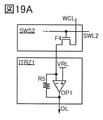
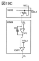
- 19A, 19B, and 19C are diagrams illustrating a configuration example of an arithmetic circuit.
- FIG. 20 is a diagram illustrating a configuration example of an arithmetic circuit.
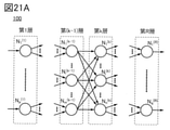
- 21, 21A and 21B are diagrams illustrating a neural network.
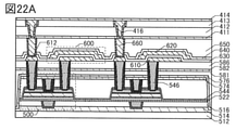
- FIG. 22A is a diagram illustrating a configuration example of the semiconductor device.
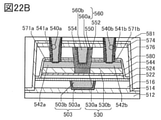
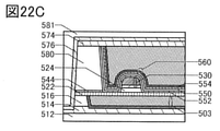
- 22B and 22C are diagrams illustrating a configuration example of a transistor.
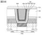
- 23A and 23B are diagrams illustrating a configuration example of a transistor.
- FIG. 24 is a diagram illustrating a configuration example of the transistor.
- 25A to 25C are diagrams for explaining a configuration example of a transistor.
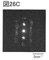
- 26A is a diagram illustrating the classification of the crystal structure of IGZO.
- FIG. 26B is a diagram illustrating an XRD spectrum of crystalline IGZO.
- FIG. 26C is a diagram illustrating a microelectron diffraction pattern of crystalline IGZO.
- FIG. 27 is a diagram illustrating a configuration example of an integrated circuit.
- 28A and 28B are diagrams illustrating application examples of integrated circuits.
- 29A and 29B are diagrams illustrating application examples of integrated circuits.
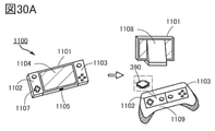
- 30A, 30B and 30C are diagrams illustrating application examples of integrated circuits.
- FIG. 31 is a diagram illustrating an application example of an integrated circuit.
- the ordinal numbers "1st”, “2nd”, and “3rd” are added to avoid confusion of the components. Therefore, the number of components is not limited. Moreover, the order of the components is not limited. Further, for example, the component referred to in “first” in one of the embodiments of the present specification or the like is the other embodiment or the component referred to in “second” in the scope of claims. It is possible. Further, for example, the component referred to in “first” in one of the embodiments of the present specification and the like may be omitted in another embodiment or in the scope of claims.
- the power supply potential VDD may be abbreviated as potential VDD, VDD, etc. This also applies to other components (eg, signals, voltages, circuits, elements, electrodes, wiring, etc.).
- the semiconductor device refers to all devices that can function by utilizing the semiconductor characteristics.
- a semiconductor circuit, an arithmetic unit, and a storage device, including a semiconductor element such as a transistor, are one aspect of a semiconductor device. It may be said that a display device (liquid crystal display device, light emission display device, etc.), projection device, lighting device, electro-optic device, power storage device, storage device, semiconductor circuit, image pickup device, electronic device, or the like has a semiconductor device.
- FIG. 1A is a diagram for explaining the semiconductor device 10A1 which is one aspect of the present invention.
- the semiconductor device 10A1 has a reference cell 21 (1) and an arithmetic cell 31 (1).
- Reference cell 21 (1) has a transistor 22, a transistor 24, and a capacitance 25.
- the arithmetic cell 31 (1) has a transistor 32, a transistor 34, and a capacitance 35.
- the transistor 22, the transistor 24, the transistor 32, and the transistor 34 have a gate and a back gate, respectively.
- a transistor having a function as a switch has a gate and a back gate
- the threshold voltage of the transistor can be controlled.
- the transistor and capacitance included in the reference cell 21 (1) and the arithmetic cell 31 (1) are connected to at least one of the wiring WSL, the wiring XCL, the wiring WCL, and the wiring that gives the ground potential.
- the reference cell 21 (1) has a function of executing a calculation operation in the calculation cell 31 (1) by passing a set current at the time of writing data and at the time of reading data. Specifically, the reference potential is held in the reference cell 21 (1) by passing a reference current at the time of data writing, and then the input data (X) given to the calculation cell 31 (1) at the time of data reading. ) Is passed through the reference cell 21 (1), and has a function of controlling the current flowing through the calculation cell 31 (1).
- the reference cell 21 (1) may be simply referred to as a cell.
- the gate of the transistor 22 is electrically connected to the wiring WSL.
- One of the source or drain of the transistor 22 is electrically connected to one of the source or drain of the transistor 24 and is also electrically connected to one electrode of the capacitance 25 via the wiring XCL.
- the other of the source or drain of the transistor 22 is electrically connected to the back gate of the transistor 24 and the other electrode of the capacitance 25.
- the transistor 22 writes the reference potential to the holding node (back gate of the transistor 24) in the reference cell 21 (1) as an on state at the time of data writing, and turns the reference potential into the reference cell 21 (1) by turning it off. Can be retained.
- the node to which the back gate of the transistor 24, the other of the source or drain of the transistor 22 and the other electrode of the capacitance 25 are connected is also referred to as a holding node.
- the holding node can be set to a potential corresponding to the current flowing through the transistor 24.
- the threshold voltage of the transistor 22 can be controlled by controlling the potential of the back gate of the transistor 22. Specifically, the threshold voltage of the transistor 22 can be lowered by increasing the potential of the back gate of the transistor 22. On the other hand, the threshold voltage of the transistor 22 can be increased by lowering the potential of the back gate of the transistor 22. Therefore, if the potential of the back gate of the transistor 22 is increased when the transistor 22 is in the on state, the on current of the transistor 22 can be increased, and the potential of the back gate of the transistor 22 is increased when the transistor 22 is in the off state. When is lowered, the off-current of the transistor 22 can be lowered.
- the gate of the transistor 24 and the other of the source or drain of the transistor 24 are connected to a wiring that gives a constant potential such as a low power supply potential (for example, a ground potential).
- the wiring that gives the ground potential functions as a wiring for passing a current between the source and the drain of the transistor 24.
- the capacity 25 changes the potential of the other electrode according to the change of the potential given to the one electrode when the other electrode is electrically suspended.
- the calculation cell 31 (1) has a function of internally holding a voltage corresponding to the current by passing a current corresponding to the weight data (W) held in the calculation cell 31 (1) at the time of data writing. .. Further, the calculation cell 31 (1) responds to the calculation of the weight data and the input data by boosting the voltage held at the time of writing the data according to the current flowing through the reference cell 21 (1) at the time of data reading. It has a function to pass a current.
- the weight data may be referred to as first data, and the input data may be referred to as second data.
- the arithmetic cell 31 (1) may be simply referred to as a cell.
- the weight data is, for example, data (weight data) corresponding to the weight parameter used in the product-sum operation of the artificial neural network.
- the gate of the transistor 32 is electrically connected to the wiring WSL.
- One of the source or drain of the transistor 32 is electrically connected to one of the source or drain of the transistor 34 and the wiring WCL.
- One electrode of the capacitance 35 is electrically connected to the wiring XCL.
- the other of the source or drain of the transistor 32 is electrically connected to the back gate of the transistor 34 and the other electrode of the capacitance 35.
- the transistor 32 writes the voltage corresponding to the weight data in the calculation cell 31 (1) by turning it on when writing data, and writes the voltage corresponding to the weight data in the calculation cell 31 (1) by turning it off. Can be held in.
- the node to which the back gate of the transistor 34, the other of the source or drain of the transistor 32, and the other electrode of the capacitance 35 are connected is also referred to as a holding node.
- the threshold voltage of the transistor 32 can be controlled by controlling the potential of the back gate of the transistor 32. Specifically, the threshold voltage of the transistor 32 can be lowered by increasing the potential of the back gate of the transistor 32. On the other hand, the threshold voltage of the transistor 32 can be increased by lowering the potential of the back gate of the transistor 32. Therefore, if the potential of the back gate of the transistor 32 is increased when the transistor 32 is in the on state, the on current of the transistor 32 can be increased, and the potential of the back gate of the transistor 32 is increased when the transistor 32 is in the off state. When is lowered, the off-current of the transistor 32 can be lowered.
- the gate of the transistor 34 and the other of the source or drain of the transistor 34 are connected to a wiring that gives a constant potential such as a low power supply potential (for example, a ground potential).
- the wiring that gives the ground potential functions as a wiring for passing a current between the source and the drain of the transistor 34.
- the capacity 35 changes the potential of the other electrode according to the change of the potential given to the one electrode when the other electrode is electrically suspended.
- the transistor 24 and the transistor 34 operate in the subthreshold region unless otherwise specified.
- the drain current Id of the transistor operating in the subthreshold region can be expressed by the equation (1).
- q is the elementary charge
- V g is the gate voltage
- V th is the threshold voltage
- ⁇ is a coefficient determined by the device structure or the like.
- k B is the Boltzmann constant
- T is the temperature.
- the drain current Id of the transistor operating in the subthreshold region does not depend on the drain voltage.
- the current flowing through the transistor 24 and the transistor 34 is the amount of current flowing when operating in the subthreshold region.
- the current in the subthreshold region of the transistor 24 and the transistor 34 can reduce the influence of the variation of the drain voltage. Therefore, the accuracy of the data obtained by the calculation can be improved.
- the subthreshold region refers to a region in which the gate voltage is lower than the threshold voltage in the graph showing the gate voltage (Vg) -drain current (Id) characteristics of the transistor.
- the subthreshold region refers to a region in which a current flows due to carrier diffusion, which deviates from the gradual channel approximation (a model that considers only drift current).
- the subthreshold region is a region in which the drain current increases exponentially with an increase in the gate voltage.
- the subthreshold region shall include a region that can be regarded as the region described above.
- the drain current when the transistor operates in the subthreshold region is called the subthreshold current.
- the subthreshold current increases exponentially with respect to the gate voltage, regardless of the drain voltage. In the circuit operation using the subthreshold current, the influence of the variation of the drain voltage can be reduced.
- the transistor 22 and the transistor 32 have a function of holding the potentials of the back gate of the transistor 24 and the back gate of the transistor 34 by turning them off. Specifically, it has a function of holding a reference potential given to the back gate of the transistor 24 via the transistor 22. Further, it has a function of holding a potential according to the data given to the back gate of the transistor 34 via the transistor 32.
- the transistor 22 and the transistor 32 are preferably transistors having a metal oxide in the channel forming region (also referred to as an OS transistor).
- the channel forming region of the transistor 22 and the transistor 32 is more preferably an oxide containing at least one of indium, gallium, and zinc.
- indium and element M includes, for example, aluminum, gallium, yttrium, copper, vanadium, beryllium, boron, titanium, iron, nickel, germanium, zirconium, molybdenum, lanthanum, lantern, etc.
- element M includes, for example, aluminum, gallium, yttrium, copper, vanadium, beryllium, boron, titanium, iron, nickel, germanium, zirconium, molybdenum, lanthanum, lantern, etc.
- cerium, neodymium, hafnium, tantalum, tungsten, gallium and the like can be mentioned), and oxides containing at least one of zinc may be used.
- the OS transistor has an extremely small leakage current, that is, the current flowing between the source and drain in the off state. Therefore, by using the OS transistor as the transistor 22 and / or the transistor 32, the leakage current of the transistor 22 and / or the transistor 32 can be suppressed, so that the power consumption of the semiconductor device 10A1 can be reduced. Specifically, since the fluctuation of the potential held in each of the back gate of the transistor 24 and the back gate of the transistor 34 can be made very small, the refreshing operation of the potential can be reduced. Further, by reducing the refresh operation, the power consumption of the semiconductor device 10A1 can be reduced. Further, by making the leakage current from the holding node to the wiring WCL or the wiring XCL very small, the cell can hold the potential of the holding node for a long time.
- the drain current per 1 ⁇ m of channel width such as less than 1 ⁇ 10 -20 A, less than 1 ⁇ 10 -22 A, or less than 1 ⁇ 10 -24 A. It is possible to pass an extremely small current.
- the OS transistor has a channel such as 1.0 ⁇ 10 -8 A or less, 1.0 ⁇ 10 -12 A or less, or 1.0 ⁇ 10 -15 A or less when the gate voltage is the threshold voltage of the transistor. A drain current per 1 ⁇ m in width can be passed. Therefore, the OS transistor can pass subthreshold currents of different sizes in the range of the gate voltage operating in the subthreshold region.
- the OS transistor can take a large range of the gate voltage operating in the subthreshold region. Specifically, when the threshold voltage of the OS transistor is Vth , in the subthreshold region, ( Vth -1.0V) or more and Vth or less, or ( Vth -0.5V) or more and Vth or less. It is possible to perform circuit operation using the gate voltage in the voltage range of.
- the OS transistor Since the bandgap of the metal oxide that functions as an oxide semiconductor is 2.5 eV or more, the OS transistor has a minimum off current. As an example, when the voltage between the source and drain is 3.5 V and the room temperature (25 ° C) is normal, the off current per 1 ⁇ m of channel width is less than 1 ⁇ 10 -20 A, 1 ⁇ 10 -22 A, or 1 ⁇ 10. It can be less than -24A . Therefore, the OS memory has an extremely small amount of charge leaked from the holding node via the OS transistor.
- the metal oxides applied to the OS transistor are Zn oxide, Zn-Sn oxide, Ga-Sn oxide, In-Ga oxide, In-Zn oxide, and In-M-Zn oxide (M is: Ti, Ga, Y, Zr, La, Ce, Nd, Sn or Hf) and the like.
- M is: Ti, Ga, Y, Zr, La, Ce, Nd, Sn or Hf
- oxides containing indium and zinc include aluminum, gallium, ittrium, copper, vanadium, beryllium, boron, silicon, titanium, iron, nickel, germanium, zirconium, molybdenum, lanthanum, cerium, neodymium, hafnium, tantalum, and tungsten. , Magnesium, etc., or a plurality of types may be contained.
- the metal oxide applied to the semiconductor layer is preferably a metal oxide having a crystal portion such as CAAC-OS, CAC-OS, and nc-OS.
- CAAC-OS is an abbreviation for c-axis-aligned crystalline oxide semiconductor ductor.
- CAC-OS is an abbreviation for Cloud-Aligned Complex Oxide semiconductor ductor.
- nc-OS is an abbreviation for nanocrystalline oxide semiconductor ductor.
- CAAC-OS has a c-axis orientation and has a crystal structure in which a plurality of nanocrystals are connected in the ab plane direction and have strain.
- the strain refers to a region where the orientation of the lattice arrangement changes between a region in which the lattice arrangement is aligned and a region in which another lattice arrangement is aligned in the region where a plurality of nanocrystals are connected.
- the CAC-OS has a function of flowing electrons (or holes) as carriers and a function of not flowing electrons as carriers. By separating the function of flowing electrons and the function of not flowing electrons, both functions can be maximized. That is, by using CAC-OS in the channel formation region of the OS transistor, both a high on current and an extremely low off current can be realized.
- the OS transistor is a storage type transistor that has a large number of electrons as carriers. Therefore, the influence of drain-induced barrier lowering (DIBL), which is one of the short-channel effects, is smaller than that of an inverting transistor having a pn junction. That is, the OS transistor has a higher resistance to the short channel effect than the Si transistor.
- DIBL drain-induced barrier lowering
- the OS transistor for the transistor 24 and the transistor 34 it is possible to operate in a wide current range in the subthreshold region, so that the current consumption can be reduced. Further, by using the OS transistor for the transistor 24 and the transistor 34, the transistor 22 and the transistor 32 can be manufactured at the same time, so that the manufacturing process of the arithmetic circuit may be shortened.
- the transistor 22, the transistor 24, the transistor 32, and the transistor 34 do not have to be OS transistors.
- the transistor 22, the transistor 24, the transistor 32, and the transistor 34 can be a Si transistor.
- the silicon for example, amorphous silicon (sometimes referred to as hydrided amorphous silicon), microcrystalline silicon, polycrystalline silicon, single crystal silicon and the like can be used.
- the transistor 22, the transistor 24, the transistor 32, and the transistor 34 shown in FIG. 1 are n-channel transistors, but the semiconductor device according to one aspect of the present invention is not limited thereto.
- the transistor 22, the transistor 24, the transistor 32, and a part or all of the transistor 34 may be replaced with a p-channel type transistor.
- the transistor 22, the transistor 24, the transistor 32, and a part or all of the transistor 34 are replaced with a p-channel type transistor, the transistor 22, the transistor 24, the transistor 32, and the transistor 34 operate as desired.
- the voltage given by the wiring may be changed as necessary.
- the above-mentioned examples of changes regarding the structure and polarity of the transistor are not limited to the transistor 22, the transistor 24, the transistor 32, and the transistor 34.
- the structure, polarity, etc. of the transistors described in other parts of the specification or the transistors shown in other drawings may be changed in the same manner.
- the wiring WSL is given a signal that controls the on or off of the transistor 22 and the transistor 32 that function as switches.
- the wiring WSL functions as a writing word line when writing data to the reference cell 21 (1) and the calculation cell 31 (1).
- the data is written in the reference cell 21 (1) or the calculation cell 31 (1) by passing a current corresponding to the desired data through the wiring XCL or the wiring WCL.
- the data is written in the reference cell 21 (1) or the calculation cell 31 (1).
- the data is written in the reference cell 21 (1) by turning on the transistor 22, and is written in the calculation cell 31 (1) by turning on the transistor 32.
- the transistor 22 and the transistor 32 can be turned on by setting the wiring WSL to H level (high level potential). Further, by turning off the transistor 22, data is held in the reference cell 21 (1), and by turning off the transistor 32, data is held in the calculation cell 31 (1). The transistor 22 and the transistor 32 can be turned off by setting the wiring WSL to L level (low level potential).
- the wiring WCL has a function of flowing an amount of current (weight current or current I Wut ) corresponding to the weight data (also referred to as first data and first input data) to the calculation cell 31 (1), or the calculation cell 31. It has a function of giving a constant potential for passing a current according to the potential held in (1).
- the wiring XCL has a current amount (reference current or current I Xut ) or input data (both second data and second input data) corresponding to the reference data for the reference cell 21 (1) and the calculation cell 31 (1). It has a function of passing a current amount (input current or current IX ) according to the current amount (referred to as).
- FIG. 1B is a diagram for explaining the semiconductor device 10B1 which is one aspect of the present invention.
- the semiconductor device 10B1 states that the gate insulating layer for the back gate of the transistor 22 and the gate insulating layer for the back gate of the transistor 32 of the semiconductor device 10A1 have a material capable of having ferroelectricity.
- the gate insulating layer with respect to the back gate of the transistor has a material capable of having ferroelectricity.
- ferroelectricity indicates a property of maintaining a polarized state even when the application of a voltage is stopped after the application of a voltage is applied to the polarization.
- the normal dielectric property indicates a property that when the application of the voltage is stopped after the polarization is applied by applying the voltage, the state of polarization is not maintained and disappears.
- Materials that can have strong dielectric properties include hafnium oxide, zirconium oxide, HfZrOX ( X is a real number larger than 0), hafnium oxide and element J1 (here, element J1 is zirconium (Zr), silicon.
- element J1 is zirconium (Zr), silicon.
- Si aluminum (Al), gadrinium (Gd), yttrium (Y), lanthanum (La), strontium (Sr), etc.
- element J2 element J2 here is hafnium) to zirconium oxide.
- Hf silicon
- Si aluminum (Al), gadrinium (Gd), yttrium (Y), lanthanum (La), strontium (Sr), etc.
- PbTIO X barium titanate strontium (BST), barium titanate, lead zirconate titanate (PZT), strontium bismuthate tantanate (SBT), bismuth ferrite (BFO).
- BST barium titanate strontium
- PZT barium titanate
- SBT strontium bismuthate tantanate
- BFO bismuth ferrite
- Barium titanate, etc. may be used as a piezoelectric ceramic having a perovskite structure.
- a laminated structure composed of a plurality of materials selected from the materials listed above or a plurality of materials selected from the materials listed above may be used. can.
- the crystal structure (characteristics) of hafnium oxide, zirconium oxide, HfZrOX , and materials obtained by adding the element J1 to hafnium oxide may change not only depending on the film forming conditions but also depending on various processes. In the present specification and the like, it is called a material that can have ferroelectricity.
- hafnium oxide, or a material having hafnium oxide and zirconium oxide as a material capable of having ferroelectricity is preferable because it can have ferroelectricity even when processed into a thin film of several nm.
- the film thickness of the material having a ferroelectricity may be 100 nm or less, preferably 50 nm or less, more preferably 20 nm or less, still more preferably 10 nm or less (typically 2 nm or more and 9 nm or less).
- HfZrOX is used as a material capable of having ferroelectricity
- a material capable of having ferroelectricity is formed by using the thermal ALD method
- a material containing no hydrocarbon also referred to as Hydrogen Carbon or HC
- HC Hydrogen Carbon
- one or both of hydrogen and carbon are contained in the material which may have a ferroelectricity
- the crystallization of the material which may have a ferroelectricity may be hindered. Therefore, as described above, it is preferable to reduce the concentration of either one or both of hydrogen and carbon in the material which may have ferroelectricity by using a precursor containing no hydrocarbon.
- a precursor containing no hydrocarbon a chlorine-based material can be mentioned.
- HfZrO x hafnium oxide and zirconium oxide
- HfCl 4 and / or ZrCl 4 may be used as the precursor.
- the oxidizing agent of the thermal ALD method is not limited to this.
- the oxidizing agent in the thermal ALD method may contain one or more selected from O 2 , O 3 , N 2 O, NO 2 , H 2 O, and H 2 O 2 .
- the crystal structure of the material that can have ferroelectricity is not particularly limited.
- the crystal structure of the material that may have strong dielectric property may be one or more selected from cubic, tetragonal, orthorhombic, and monoclinic.
- a material that can have ferroelectricity it is preferable to have an orthorhombic crystal structure because ferroelectricity is exhibited.
- a composite structure having an amorphous structure and a crystal structure may be used as a material that can have ferroelectricity.
- Materials that can have isoelectricity include silicon oxide, silicon oxide, silicon nitride, silicon nitride, silicon oxide with fluorine added, silicon oxide with carbon added, silicon oxide with carbon and nitrogen added, and vacancies. Silicon oxide having the above can be used. In particular, silicon oxide and silicon nitride nitride are preferable because they are heat-stable.
- the polarization state of the gate insulating layer with respect to the back gate can be controlled by controlling the potential of the back gate of the transistor 22. Thereby, the threshold voltage of the transistor 22 can be controlled. Similarly, by controlling the potential of the back gate of the transistor 32, the polarization state of the gate insulating layer with respect to the back gate can be controlled, whereby the threshold voltage of the transistor 32 can be controlled.
- the semiconductor device 10B1 even if the gate insulating layer with respect to the back gate of the transistor 22 or the transistor 32 is polarized and then the supply of the potential to the back gate is stopped, the gate insulating layer maintains the polarized state. Can be done. Therefore, it is not necessary to continue to supply the potential to the back gates of the transistor 22 and the transistor 32. Therefore, the semiconductor device 10B1 can be a semiconductor device having low power consumption.
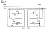
- FIG. 2A is a diagram for explaining the semiconductor device 10A2 which is one aspect of the present invention.
- the description of the same configuration as that of the semiconductor device 10A1 may be omitted.
- the semiconductor device 10A2 has a reference cell 21 (2) and an arithmetic cell 31 (2).
- the reference cell 21 (2) has a transistor 22, a transistor 24, and a capacity 25, similarly to the reference cell 21 (1).
- the calculation cell 31 (2) has a transistor 32, a transistor 34, and a capacity 35, similarly to the calculation cell 31 (1).
- the gate of the transistor 22 is electrically connected to the wiring WSL.
- One of the source or drain of the transistor 22 is electrically connected to one of the source or drain of the transistor 24 and the wiring XCL.
- the other of the source or drain of the transistor 22 is electrically connected to the gate of the transistor 24 and one electrode of the capacitance 25.
- the transistor 22 writes the reference potential to the holding node (gate of the transistor 24) in the reference cell 21 (2) as an on state at the time of data writing, and holds the reference potential in the reference cell 21 (2) by turning it off. can do.
- a node to which the gate of the transistor 24, the other of the source or drain of the transistor 22 and one of the electrodes of the capacitance 25 are connected is also referred to as a holding node.
- the holding node can be set to a potential corresponding to the current flowing through the transistor 24.
- the other electrode of the source or drain of the transistor 24 and the other electrode of the capacitance 25 are connected to a wiring that gives a constant potential such as a low power supply potential (for example, a ground potential).
- the wiring that gives the ground potential functions as a wiring for passing a current between the source and the drain of the transistor 24.
- the back gate of the transistor 24 is electrically connected to the wiring XCL.
- the gate of the transistor 32 is electrically connected to the wiring WSL.
- One of the source or drain of the transistor 32 is electrically connected to one of the source or drain of the transistor 34 and the wiring WCL.
- the other of the source or drain of the transistor 32 is electrically connected to one electrode of the gate and capacitance 35 of the transistor 34.
- the transistor 32 writes the voltage corresponding to the weight data in the calculation cell 31 (2) by turning it on when writing data, and writes the voltage corresponding to the weight data in the calculation cell 31 (2) by turning it off. Can be held in.
- a node to which the gate of the transistor 34, the other of the source or drain of the transistor 32, and one of the electrodes of the capacitance 35 are connected is also referred to as a holding node.
- the other of the source or drain of the transistor 34 is connected to a wiring that gives a constant potential such as a low power supply potential (for example, a ground potential).
- the wiring that gives the ground potential functions as a wiring for passing a current between the source and the drain of the transistor 34.
- the back gate of the transistor 34 is electrically connected to the wiring XCL.
- the transistor 22 and the transistor 32 have a function of holding the potentials of the gate of the transistor 24 and the gate of the transistor 34 by turning them off. Specifically, it has a function of holding a reference potential given to the gate of the transistor 24 via the transistor 22. Further, it has a function of holding a potential according to the data given to the gate of the transistor 34 via the transistor 32.
- the OS transistor has an extremely small leakage current, that is, the current flowing between the source and drain in the off state. Therefore, by using the OS transistor as the transistor 22 and / or the transistor 32, the leakage current of the transistor 22 and / or the transistor 32 can be suppressed, so that the power consumption of the semiconductor device 10A2 can be reduced. Specifically, since the fluctuation of the potential held in each of the gate of the transistor 24 and the gate of the transistor 34 can be made very small, the refreshing operation of the potential can be reduced. Further, by reducing the refresh operation, the power consumption of the semiconductor device 10A2 can be reduced. Further, by making the leakage current from the holding node to the wiring WCL or the wiring XCL very small, the cell can hold the potential of the holding node for a long time.
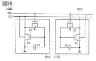
- FIG. 2B is a diagram for explaining the semiconductor device 10B2 which is one aspect of the present invention.
- the semiconductor device 10B2 states that the gate insulating layer for the back gate of the transistor 22 and the gate insulating layer for the back gate of the transistor 32 of the semiconductor device 10A2 have a material capable of having ferroelectricity.
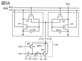
- FIG. 3A is a diagram for explaining the semiconductor device 10A3 which is one aspect of the present invention.
- the description of the same configuration as that of the semiconductor device 10A1 may be omitted.
- the semiconductor device 10A3 has a reference cell 21 (3) and an arithmetic cell 31 (3).
- the reference cell 21 (3) has a transistor 22, a transistor 24, and a capacity 25, similarly to the reference cell 21 (1).
- the calculation cell 31 (3) has a transistor 32, a transistor 34, and a capacity 35, similarly to the calculation cell 31 (1).
- the transistor 22, the transistor 24, the transistor 32, and the transistor 34 have a gate and a back gate, respectively.
- the gate of the transistor 22 is electrically connected to the wiring WSL.
- One of the source or drain of the transistor 22 is electrically connected to one of the source or drain of the transistor 24 and the wiring XCL.
- the other of the source or drain of the transistor 22 is electrically connected to the back gate of the transistor 24 and one electrode of the capacitance 25.
- the transistor 22 writes the reference potential to the holding node (back gate of the transistor 24) in the reference cell 21 (3) as an on state at the time of data writing, and turns the reference potential into the reference cell 21 (3) by turning it off. Can be retained.
- a node to which the back gate of the transistor 24, the other of the source or drain of the transistor 22, and one of the electrodes of the capacitance 25 are connected is also referred to as a holding node.
- the holding node can be set to a potential corresponding to the current flowing through the transistor 24.
- the other electrode of the source or drain of the transistor 24 and the other electrode of the capacitance 25 are connected to a wiring that gives a constant potential such as a low power supply potential (for example, a ground potential).
- the wiring that gives the ground potential functions as a wiring for passing a current between the source and the drain of the transistor 24.
- the gate of the transistor 24 is electrically connected to the wiring XCL.
- the gate of the transistor 32 is electrically connected to the wiring WSL.
- One of the source or drain of the transistor 32 is electrically connected to one of the source or drain of the transistor 34 and the wiring WCL.
- the other of the source or drain of the transistor 32 is electrically connected to the back gate of the transistor 34 and one electrode of the capacitance 35.
- the transistor 32 writes the voltage corresponding to the weight data in the calculation cell 31 (3) by turning it on when writing data, and writes the voltage corresponding to the weight data in the calculation cell 31 (3) by turning it off. Can be held in.
- a node to which the back gate of the transistor 34, the other of the source or drain of the transistor 32, and one of the electrodes of the capacitance 35 are connected is also referred to as a holding node.
- the other of the source or drain of the transistor 34 is connected to a wiring that gives a constant potential such as a low power supply potential (for example, a ground potential).
- the wiring that gives the ground potential functions as a wiring for passing a current between the source and the drain of the transistor 34.
- the gate of the transistor 34 is electrically connected to the wiring XCL.
- the transistor 22 and the transistor 32 have a function of holding the potentials of the back gate of the transistor 24 and the back gate of the transistor 34 by turning them off. Specifically, it has a function of holding a reference potential given to the back gate of the transistor 24 via the transistor 22. Further, it has a function of holding a potential according to the data given to the back gate of the transistor 34 via the transistor 32.
- the OS transistor has an extremely small leakage current, that is, the current flowing between the source and drain in the off state. Therefore, by using the OS transistor as the transistor 22 and / or the transistor 32, the leakage current of the transistor 22 and / or the transistor 32 can be suppressed, so that the power consumption of the semiconductor device 10A3 can be reduced. Specifically, since the fluctuation of the potential held in each of the back gate of the transistor 24 and the back gate of the transistor 34 can be made very small, the refreshing operation of the potential can be reduced. Further, by reducing the refresh operation, the power consumption of the semiconductor device 10A3 can be reduced. Further, by making the leakage current from the holding node to the wiring WCL or the wiring XCL very small, the cell can hold the potential of the holding node for a long time.
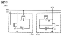
- FIG. 3B is a diagram for explaining the semiconductor device 10B3 which is one aspect of the present invention.
- the semiconductor device 10B3 states that the gate insulating layer for the back gate of the transistor 22 and the gate insulating layer for the back gate of the transistor 32 of the semiconductor device 10A3 have a material capable of having ferroelectricity.
- FIG. 4A is a diagram for explaining the semiconductor device 10C1 which is an aspect of the present invention
- FIG. 5A is a diagram for explaining the semiconductor device 10C2 which is an aspect of the present invention
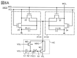
- FIG. 6A is a diagram for explaining the semiconductor device 10C2. It is a figure for demonstrating the semiconductor device 10C3 which is one aspect of this invention.
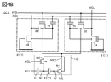
- the semiconductor device 10C1 states that the back gate of the transistor 22 and the back gate of the transistor 32 included in the semiconductor device 10A1 are electrically connected to the circuit HC.
- the semiconductor device 10C2 states that the back gate of the transistor 22 and the back gate of the transistor 32 included in the semiconductor device 10A2 are electrically connected to the circuit HC.
- the semiconductor device 10C3 states that the back gate of the transistor 22 and the back gate of the transistor 32 included in the semiconductor device 10A3 are electrically connected to the circuit HC.
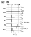
- the circuit HC has a function as a holding circuit for holding the potential of the back gate of the transistor 22 and the potential of the back gate of the transistor 32.
- the circuit HC has a transistor M1, a transistor M2, a capacitance C1, and a capacitance FEC1.
- the transistor M1 and the transistor M2 have a gate and a back gate, respectively.
- each of the transistor M1 and the transistor M2 is an OS transistor.
- the OS transistor has an extremely small off current. Therefore, by using the OS transistor as the transistor M1 and the transistor M2, the potential of the back gate of the transistor 22 and the potential of the back gate of the transistor 32 can be held for a long time.
- Capacity FEC1 is a capacity having a material that can have ferroelectricity as a dielectric.
- a capacitance using a material capable of having ferroelectricity as a dielectric is referred to as a ferroelectric capacitor.
- the circuit symbol of the ferroelectric capacitor (for example, the capacitance FEC1) is the circuit symbol of the capacitance with diagonal lines added as shown in FIGS. 4A, 5A, and 6A. Further, as another circuit symbol, as shown in FIGS. 4B, 5B, and 6B, a plurality of diagonal lines may be added between two lines parallel to each other in the capacity circuit symbol.
- the circuit HC is electrically connected to the reference cell 21 and the calculation cell 31.
- the back gate of the transistor 22 and the back gate of the transistor 32 are electrically connected to one of the source or drain of the transistor M1, the back gate of the transistor M1, and the source or drain of the transistor M2. ..
- the other of the source or drain of the transistor M1 is electrically connected to the wiring VIL.
- the gate of the transistor M1 is electrically connected to one electrode of the capacitance FEC1.
- the other of the source or drain of the transistor M2 is electrically connected to the other electrode of the capacitance FEC1 and one electrode of the capacitance C1.
- the gate of the transistor M2 is electrically connected to the wiring VGL.
- the other electrode of capacitance C1 is electrically connected to the wiring VCL.
- the electrical connection point between the gate of the transistor M1 and one electrode of the capacitance FEC1 is referred to as a node N1.
- the electrical connection point between the other electrode of the capacitance FEC1, one electrode of the capacitance C1, and the other of the source or drain of the transistor M2 is referred to as a node N2.
- the electrical connection point between one of the source or drain of the transistor M1, the back gate of the transistor M1, and one of the source or drain of the transistor M2 is referred to as a node NBG. That is, the potential of the node NBG can be the potential given to the back gate of the transistor 22 and the back gate of the transistor 32.
- the node N1 Since the node N1 is not electrically connected to circuit elements, terminals, wirings, etc. other than the gate of the transistor M1 and one electrode of the capacitance FEC1, the voltage is directly input to the node N1 from the voltage source or the like. There is no. Therefore, the node N1 is in a floating state.
- the initial potential of the node N1 can be determined at the time of manufacturing the semiconductor device (specifically, for example, at the time of forming the circuit HC).
- Wiring VIL functions as wiring that gives a constant potential.
- the constant potential may be, for example, a low level potential, a ground potential, a negative potential, or the like when the threshold voltage of the transistor 22 and the transistor 32 is shifted to the positive side. Further, for example, when the threshold voltage of the transistor 22 and the transistor 32 is shifted to the negative side, it can be set to a high level potential, a positive potential, or the like.
- the wiring VCL functions as a wiring for giving a potential for polarizing the material having a ferroelectricity contained in the capacitance FEC1.
- the potential may be a positive potential or the like.
- the wiring VCL may be supplied with a potential that does not polarize the material contained in the capacitance FEC1 that may have ferroelectricity.
- the wiring VGL functions as wiring that supplies a signal potential for controlling switching between the on state and the off state of the transistor M2. For example, by setting the potential of the wiring VGL to a high level potential, the transistor M2 can be turned on, and by setting the potential of the wiring VGL to a low level potential, the transistor M2 can be turned off.
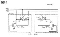
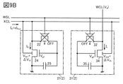
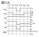
- FIG. 7A shows an outline of an operation at the time of writing data
- FIG. 7B shows an outline of an operation at the time of reading data.
- a reference cell unit 20 having a plurality of reference cells 21_1 to 21_m (corresponding to the reference cell 21 in FIG. 1A and the like), and a plurality of calculation cells 31_1, 1 to 31_m, n (calculations in FIG. 1A and the like).
- a calculation cell unit 30 including (corresponding to cell 31) is provided.
- a plurality of wiring XCLs are illustrated as wirings XCL_1 to XCL_m.
- a plurality of wiring WCLs are illustrated as wirings WCL_1 to WCL_n. Both m and n are integers of 1 or more.
- the cells included in the reference cell unit 20 and the calculation cell unit 30 are arranged in a matrix of n + 1 in the row direction and m in the column direction.
- the reference cell unit 20 and the calculation cell unit 30 may have two or more cells in the row direction and one or more cells in the column direction, as long as they are arranged in a matrix.
- the terminal CP of the reference cell 21 in the reference cell unit 20 corresponds to one electrode of the capacitance 25 as shown in FIG. 1A, the back gate of the transistor 24 as shown in FIG. 2A, or the gate of the transistor 24 as shown in FIG. 3A.
- the terminal TW of the reference cell 21 in the reference cell unit 20 corresponds to a terminal to which one of the source or drain of the transistor 22 of FIGS. 1A, 2A, and 3A and one of the source or drain of the transistor 24 are connected. do.
- the terminal CP of the arithmetic cell 31 in the arithmetic cell unit 30 corresponds to one electrode of the capacitance 35 of FIG. 1A or the like, the back gate of the transistor 34 of FIG. 2A or the like, or the gate of the transistor 34 of FIG. 3A or the like.
- the terminal TX of the arithmetic cell 31 in the arithmetic cell unit 30 corresponds to a terminal to which one of the source or drain of the transistor 32 and one of the source or drain of the transistor 34 in FIGS. 1A, 2A, and 3A are connected. ..
- a current I Xut is passed through the reference cell 21 in each row.
- the current given to each row is the normalized current I Xut , which is equal.
- the current I Xut corresponds to the amount of current (reference current) according to the reference data. Since it is connected to the calculation cell 31 in each row via a capacitance, no current flows.
- the reference cell 21 operates so as to maintain a voltage corresponding to the flowing current.
- currents I W1 to I Wn are passed through the arithmetic cells in each column.
- the currents I W1 to I Wn may be different for each column.
- currents IX1 to IXm are passed through the reference cell 21 in each row.
- the currents IX1 to IXm may be different for each row.
- the current I Xut is preferably equal to the current I Wut .
- the voltage held in the reference cell 21 is boosted by the currents IX1 to IXm . Since the wirings XCL_1 to XCL_m are also boosted in response to this boosting, the voltage held by the capacitive coupling of the capacitance 35 in the arithmetic cell 31 is boosted. Then, the potentials of the wirings WCL_1 to WCL_n are set to the voltage Vd. At this time, the current Ir flowing through the transistor 34 corresponds to the product of the current value (I w ) held in the calculation cell 31 at the time of writing the data and the current value (I x ) flowing through the reference cell 21 at the time of reading the data. (Currents Ir11 to Irmn ). By estimating the sum of the currents Ir11 to Irm flowing in each column, it is possible to output data corresponding to the calculation result of the sum of products of the input data and the weight data.
- the size of the transistor 22 and the transistor 24 (for example, channel length, channel width, transistor configuration, etc.) included in each of the cells included in the reference cell portion 20 are equal to each other. Further, it is preferable that the size of the transistor 32 and the transistor 34 included in each of the cells included in the arithmetic cell unit 30 are equal to each other. Further, it is preferable that the size of the transistor 22 and the size of the transistor 32 are equal to each other. Further, it is preferable that the size of the transistor 24 and the size of the transistor 34 are equal to each other.
- the sizes of the transistors 22 included in the reference cells 21_1, 1 to the reference cells 21_m, n are made equal to each other, and the sizes of the transistors 24 included in the reference cells 21_1, 1 to the reference cells 21_m, n are equalized.
- each of the reference cells 21_1, 1 to the reference cells 21_m, n can perform substantially the same operation when the conditions are the same.
- the conditions are the same, for example, the input potential of the transistor 22 to the source, drain, gate, etc., the input potential of the transistor 24 to the source, drain, gate, etc., reference cells 21_1 to 1 to reference cell 21_m, It means that the voltage and the like held in each of n are equal. Further, for example, by equalizing the sizes of the transistors 32 included in each of the arithmetic cells 31_1 to 31_m and equalizing the sizes of the transistors 34 included in each of the arithmetic cells 31_1 to the arithm, for example. In the calculation cell 31_1 to the calculation cell 31_m, the operation and the result of the operation can be substantially the same.
- the conditions are the same, almost the same operation can be performed.
- the conditions are the same, for example, the input potentials of the transistor 32 to the source, drain, gate, etc., the input potentials of the transistor 34 to the source, drain, gate, etc., and each of the calculation cells 31_1 to the calculation cell 31_m. It means that the held voltage etc. are equal.
- the wiring WSL is set to H level, and the transistor 22 and the transistor 32 are set to the ON state (ON).
- a current I Xut which corresponds to a reference current, is passed through the wiring XCL. Further, a current I W is passed through the wiring WCL.
- the transistor 22 is turned on.
- the potential of the holding node to which the back gate of the transistor 24 is electrically connected is such that the threshold voltage of the transistor 24 becomes V th1 .
- the transistor 24 can pass the current of the current I Xut between the source and the drain of the transistor 24.
- the threshold voltage of the transistor 24 can be set so that the current flowing between the source and the drain of the transistor 24 is IXut . In the present specification and the like, such an operation may be referred to as "setting (programming) the current flowing between the source and drain of the transistor 24 of the reference cell 21 (1) in IXut " and the like.
- the transistor 32 is turned on.
- the potential of the holding node to which the back gate of the transistor 34 is electrically connected is such that the threshold voltage of the transistor 34 becomes V th2 .
- the current flowing between the source and drain of the transistor 34 of the arithmetic cell 31 (1) is set to I w .
- the threshold voltage of the transistor 34 is set so that the current flowing between the source and the drain of the transistor 34 is I w .
- the current I Xut applied to the reference cell 21 (1) via the wiring XCL at the time of writing data can be expressed by the equation (2).
- a ground potential is applied to the gate of the transistor 24 and the source or drain of the transistor 24.
- the current IW given to the calculation cell 31 (1) via the wiring WCL at the time of data writing can be expressed by the equation (3).
- a ground potential is applied to the gate of the transistor 34 and the source or drain of the transistor 34.
- the current I w can be expressed by the product of the weight data w and the normalized current I Wut .
- a period for holding the set current can be provided in the period between the time of writing the data and the time of reading the data.
- the transistor 22 and the transistor 32 are turned off.
- the transistor 22 and the transistor 32 can continue to hold the potential of the holding node corresponding to the set current by using the OS transistor.
- the wiring WSL is set to the L level, and the transistor 22 is set to the OFF state (OFF).
- a current I x corresponding to an input current is passed through the wiring XCL.
- the potential of the holding node to which the back gate of the transistor 24 is electrically connected fluctuates due to capacitive coupling via the capacitance 25 due to the current IX flowing through the transistor 24, whereby the threshold voltage of the transistor 24 changes. It fluctuates with V th1 + ⁇ V th .
- the potential of the wiring XCL also fluctuates.
- the wiring WSL is set to the L level, and the transistor 32 is set to the OFF state (OFF). Therefore, the holding node of the arithmetic cell 31 (1) is electrically in a floating state (floating).
- the potential of the holding node of the arithmetic cell 31 (1) fluctuates due to the capacitive coupling of the capacitance 35 due to the fluctuation of the potential of the wiring XCL due to the operation of the reference cell 21 (1), and the threshold voltage of the transistor 34 becomes V th2 + ⁇ V. It fluctuates with th . As a result, a current Ir flows between the source and drain of the transistor 34.
- the current IX applied to the reference cell 21 (1) via the wiring XCL at the time of data reading can be expressed by the equation (4).
- a ground potential is applied to the gate of the transistor 24 and the source or drain of the transistor 24.
- the input data x can be represented by the formula (5).
- the current IX can be represented by the product of the input data x and the normalized current IXut .
- the wiring WCL is set to a voltage V d so that a current flows through the calculation cell 31 (1) in each row. Then, the threshold voltage of the transistor 34 of the arithmetic cell 31 (1) changes to V th2 + ⁇ V th , so that the current Ir flowing through the transistor 34 can be expressed by the equation (6).
- a ground potential is applied to the gate of the transistor 34 and the source or drain of the transistor 34.
- Ir in equations (3), (5) to (6) can be estimated as a current corresponding to the product of the weight data w and the input data x. Since the current flowing in the calculation cell 31 (1) of each row can be added up, by outputting the current flowing in the wiring WCL to the outside, the calculation result of the product-sum calculation process according to the weight data w and the input data x. It is possible to output a signal according to the above.
- the wiring WSL is set to H level, and the transistor 22 and the transistor 32 are set to the ON state (ON).
- the transistor 22 is turned on.
- the potential of the holding node to which the gate of the transistor 24 is electrically connected is V g1 .
- the potential of the back gate of the transistor 24 is such that the threshold voltage of the transistor 24 becomes V th1 .
- the transistor 24 can pass the current of the current I Xut between the source and the drain of the transistor 24.
- the transistor 32 is turned on.
- the potential of the holding node to which the gate of the transistor 34 is electrically connected is V g 2 .
- the potential of the back gate of the transistor 34 is such that the threshold voltage of the transistor 34 becomes V th2 .
- the current flowing between the source and drain of the transistor 34 of the arithmetic cell 31 (2) is set to I w .
- the current I Xut applied to the reference cell 21 (2) via the wiring XCL at the time of writing data can be expressed by the equation (7).
- a ground potential is applied to the other of the source or drain of the transistor 24.
- the current IW applied to the calculation cell 31 (2) via the wiring WCL at the time of data writing can be expressed by the equation (8).
- a ground potential is applied to the other of the source and drain of the transistor 34.
- the current I w can be expressed by the product of the weight data w and the normalized current I Wut .
- the wiring WSL is set to the L level, and the transistor 22 is set to the OFF state (OFF).
- a current I x corresponding to an input current is passed through the wiring XCL.
- the potential of the back gate of the transistor 24 fluctuates to a potential such that the threshold voltage of the transistor 24 becomes V th1 + ⁇ V th when the current IX flows through the transistor 24.
- the potential of the wiring XCL also fluctuates.
- the wiring WSL is set to the L level, and the transistor 32 is set to the OFF state (OFF).
- the potential of the back gate of the transistor 34 also fluctuates, and the threshold voltage of the transistor 34 fluctuates as V th2 + ⁇ V th .
- a current Ir flows between the source and drain of the transistor 34.
- the current IX applied to the reference cell 21 (2) via the wiring XCL when reading data can be expressed by the equation (9).
- a ground potential is applied to the other of the source or drain of the transistor 24.
- the input data x can be represented by the formula (10).
- the current IX can be represented by the product of the input data x and the normalized current I Xut .
- the wiring WCL is set to a voltage V d so that a current flows through the calculation cell 31 (2) in each row. Then, the threshold voltage of the transistor 34 of the arithmetic cell 31 (2) changes to V th2 + ⁇ V th , so that the current Ir flowing through the transistor 34 of the arithmetic cell 31 (2) is expressed by the equation (11). Can be done.
- a ground potential is applied to the other of the source and drain of the transistor 34.
- Ir in equations (8) and (10) to (11) can be estimated to be a current corresponding to the product of the weight data w and the input data x. Since the current flowing in the calculation cell 31 (2) of each row can be added up, by outputting the current flowing in the wiring WCL to the outside, the calculation result of the product-sum calculation process according to the weight data w and the input data x. It is possible to output a signal according to the above.
- the wiring WSL is set to H level, and the transistor 22 and the transistor 32 are set to the ON state (ON).
- the transistor 22 is turned on.
- the potential of the holding node to which the back gate of the transistor 24 is electrically connected is such that the threshold voltage of the transistor 24 becomes V th1 .
- the potential of the gate of the transistor 24 is V g .
- the transistor 24 can pass the current of the current I Xut between the source and the drain of the transistor 24.
- the threshold voltage of the transistor 24 can be set so that the current flowing between the source and the drain of the transistor 24 becomes IXut when the potential of the gate of the transistor 24 is V g .
- the transistor 32 is turned on.
- the potential of the holding node to which the back gate of the transistor 34 is electrically connected is such that the threshold voltage of the transistor 24 becomes V th2 .
- the potential of the gate of the transistor 34 is V g .
- the current flowing between the source and drain of the transistor 34 of the arithmetic cell 31 (3) is set to I w .
- the threshold voltage of the transistor 34 is set so that the current flowing between the source and drain of the transistor 34 becomes I w when the potential of the gate of the transistor 34 is V g .
- the current I Xut applied to the reference cell 21 (3) via the wiring XCL at the time of writing data can be expressed by the equation (12).
- a ground potential is applied to the other of the source or drain of the transistor 24.
- the current IW given to the calculation cell 31 (3) via the wiring WCL at the time of data writing can be expressed by the equation (13).
- a ground potential is applied to the other of the source and drain of the transistor 34.
- the current I w can be expressed by the product of the weight data w and the normalized current I Wut .
- the wiring WSL is set to the L level, and the transistor 22 is set to the OFF state (OFF).
- a current I x corresponding to an input current is passed through the wiring XCL.
- the potential of the gate of the transistor 24 fluctuates as V g + ⁇ V g due to the current I x flowing through the transistor 24, and the potential of the wiring XCL also fluctuates.
- the wiring WSL is set to the L level, and the transistor 32 is set to the OFF state (OFF).
- the potential of the gate of the transistor 34 With the fluctuation of the potential of the wiring XCL due to the operation of the reference cell 21 (3), the potential of the gate of the transistor 34 also fluctuates, and becomes V g + ⁇ V g .
- the potential of the gate of the transistor 34 fluctuates as V g + ⁇ V g , a current Ir flows between the source and the drain of the transistor 34 of the arithmetic cell 31 (3).
- the current IX applied to the reference cell 21 (3) via the wiring XCL at the time of data reading can be expressed by the equation (14).
- a ground potential is applied to the other of the source or drain of the transistor 24.
- the input data x can be represented by the formula (15).
- the current IX can be represented by the product of the input data x and the normalized current I Xut .
- the wiring WCL is set to a voltage V d so that a current flows through the calculation cell 31 (3) in each row. Then, the potential of the gate of the transistor 34 of the arithmetic cell 31 (3) changes to V g + ⁇ V g , so that the current Ir flowing through the transistor 34 of the arithmetic cell 31 (3) is expressed by the equation (16). Can be done. Here, it is assumed that a ground potential is applied to the other of the source and drain of the transistor 34.
- Ir in equations (13) and (15) to (16) can be estimated to be a current corresponding to the product of the weight data w and the input data x. Since the current flowing in the calculation cell 31 (3) of each row can be added up, by outputting the current flowing in the wiring WCL to the outside, the calculation result of the product-sum calculation process according to the weight data w and the input data x. It is possible to output a signal according to the above.
- FIG. 11A is a timing chart showing an operation example of the circuit HC, and is a wiring VCL, a wiring VGL, a wiring VIL, a node N1, a node N2, and a node NBG at a time between and near the time T11 and the time T16. It shows the change of each potential of.
- FIG. 11A shows an operation example of writing the potential to the capacitance FEC1. Further, in FIG. 11A, the high level potential is described as “High” and the low level potential is described as “Low”.
- VCL is given the potential V FC1
- the wiring VGL is given the high level potential
- the wiring VIL is given the potential V IN1 .
- the V FC1 can be, for example, a positive potential, a high level potential, a ground potential, or the like
- the V IN 1 can be, for example, a positive potential, a high level potential, a ground potential, or the like.
- the potential V 11 of the node N1 is lower than the potential V 21 of the node N2.
- the voltage between the first terminal and the second terminal of the capacitance FEC1 is V 11 ⁇ V 12 , but at this voltage, the dielectric contained in the capacitance FEC1 which can have ferroelectricity does not cause polarization. It shall be.
- the potential V 11 of the node N1 is the potential V 21 of the node N2 as long as the dielectric contained in the capacitance FEC1 and which can have strong dielectric property does not cause polarization. It may be a potential equal to or higher than the potential V 21 instead of a lower potential.
- the transistor M2 Since the gate of the transistor M2 is given a high level potential from the wiring VGL, the transistor M2 is turned on. Therefore, a conduction state is established between the node N2 and the node NBG, and the potential VBG1 of the node NBG becomes substantially equal to the potential V21 of the node N2.
- a low level potential is applied to the wiring VGL between the time T12 and the time T13.
- the gate of the transistor M2 is given a low level potential from the wiring VGL, so that the transistor M2 is turned off.
- the node N2 is in a floating state.
- the potential V FC1 given by the wiring VCL changes to the potential V FC2 .
- the potential V FC2 has a potential lower than that of V FC1 and has a potential at which polarization occurs in a dielectric contained in the capacitance FEC1 which can have ferroelectricity.
- the potential given by the wiring VCL changes from V FC1 to V FC2 , and the potential of the node N2 also changes according to the voltage change due to the capacitive coupling in the capacitance C1.
- the potential of the node N2 changes from V 21 to V 22 between the time T13 and the time T14. Since the potential V FC2 has a lower potential than V FC1 , the potential V 22 has a lower potential than V 21 .
- the potential of the node N1 changes from V21 to V22, and the potential of the node N1 also changes according to the voltage change due to the capacitive coupling in the capacitive FEC1 .
- the voltage between the first terminal and the second terminal of the capacitance FEC1 becomes V 12 ⁇ V 22 , and the polarization is caused by the dielectric material contained in the capacitance FEC1 which can have ferroelectricity in the capacitance FEC1. It shall happen. That is, it is assumed that the write operation to the capacitance FEC1 is performed at this timing.
- the potential V IN1 given by the wiring VIL is set as a positive potential, a high level potential, etc., and the potential V IN1 is given to the transistor M1 from the wiring VIL, so that the potential of the node N1 is passed between the gate of the transistor M1 and the first terminal. May be able to be boosted.
- the voltage V 12 ⁇ V 22 between the first terminal and the second terminal of the capacitance FEC1 can be increased, and the dielectric material which can easily have the ferroelectricity contained in the capacitance FEC1 can be obtained. It may be possible to cause polarization.
- the potential V FC2 given by the wiring VCL changes to V FC1 . That is, the potential given by the wiring VCL between the time T14 and the time T15 is assumed to be equal to the potential given by the wiring VCL at the time before the time T13.
- the potential V FC2 given by the wiring VCL changes to V FC1 , and the potential of the node N2 returns from V 22 to V 21 .
- the potential V 12 of the node N1 also changes due to the capacitive coupling of the capacitance FEC1. Since the operation between the time T13 and the time T14 causes polarization in the dielectric contained in the capacitance FEC1 that can have strong dielectric property, the potential of the node N1 does not return to the original potential V11. , The potential is higher than the potential V 12 and lower than the potential V 11 . In this operation example, it is assumed that the potential of the node N1 changes from the potential V 12 to the potential V 13 between the time T14 and the time T15.
- the potential V 13 is lower than the potential V 21 and the potential V IN 1.
- the gate-source voltage V 13 -V IN1 of the transistor M1 is lower than the threshold voltage of the transistor M1, and the transistor M1 is turned off.
- a high level potential is given to the wiring VGL between the time T15 and the time T16.
- the gate of the transistor M2 is given a high level potential from the wiring VGL, so that the transistor M2 is turned on.
- FIG. 11B is a timing chart showing an operation example of the circuit HC, and is a wiring VCL, a wiring VGL, a wiring VIL, a node N1, a node N2, and a node NBG at a time between the time T21 and the time T24 and in the vicinity thereof. It shows the change of each potential of.
- FIG. 11B shows an operation example of writing the potential to the back gate of the transistor 22 and the transistor 32. Further, in FIG. 11B, the high level potential is described as “High” and the low level potential is described as “Low”.
- the potential V IN1 given by the wiring VIL changes to the potential V IN2 .
- the potential V IN 2 is lower than the potential V IN 1. Further, the potential V IN 2 can be, for example, a negative potential, a low level potential, or the like.
- V IN2 Since the potential V IN2 is given to the first terminal of the transistor M1 from the wiring VIL, the gate-source voltage of the transistor M1 becomes V 13 -V IN 2 .
- V 13 ⁇ V IN2 is a voltage higher than the threshold voltage of the transistor M1.
- V 13 ⁇ V IN2 By setting V 13 ⁇ V IN2 to a voltage higher than the threshold voltage of the transistor M1, the transistor M1 is turned on. Further, since the wiring VGL is given a high level potential and the transistor M2 is also in the ON state, the wiring VIL is connected to the node N2 from the wiring VIL via the transistor M1, the node NBG, and the transistor M2. A potential is supplied.
- the potentials of the node N2 and the node NBG each decrease from V21.
- the potentials of the node N2 and the node NBG decrease from V 21 by the voltage ⁇ V BG between the time T22 and the time T23.
- the potentials of the node N2 and the node NBG are lowered by ⁇ VBG to become VBG2 .
- the potential of the node N2 decreases from V21 to VBG2
- the potential V13 of the node N1 also decreases due to the capacitive coupling of the capacitance FEC1 .
- the potential of the node N1 is assumed to be V 13 ⁇ ⁇ V BG between the time T22 and the time T23.
- ⁇ is a capacity coupling coefficient in the capacity FEC1.
- the potential V IN 2 given by the wiring VIL changes to V IN 1. That is, the potential given by the wiring VIL between the time T23 and the time T24 is assumed to be equal to the potential given by the wiring VIL at the time before the time T22.
- V 13 ⁇ V BG has a lower potential than V 13
- V 13 has a lower potential than V IN 1.
- V 13 ⁇ V IN1 is lower than the threshold voltage of the transistor M1
- V 13 ⁇ V BG ⁇ V IN1 is also lower than the threshold voltage of the transistor M1. As a result, the transistor M1 is turned off between the time T23 and the time T24.
- the voltage VBG2 can be written to the node NBG of the circuit HC.
- VBG2 can be set to a negative potential, and VBG2 can be written to the node NBG of the circuit HC as a negative potential.
- the gate-source voltage of the transistor M1 can be made lower than the threshold voltage to turn off the transistor M1
- the negative potential VBG2 of the node NBG can be held for a long time.
- the negative potential VBG2 can be applied to the back gates of the transistor 22 and the transistor 32 for a long time. Further, depending on the situation, the same operation may be performed to refresh the negative potential held in the node NBG.
- the circuit HC When it is desired to lower the potential of the node NBG, for example, the circuit HC may be operated as shown in the timing chart shown in FIG. 12A.
- the timing chart of FIG. 12A shows changes in the potentials of the wiring VCL, the wiring VGL, the wiring VIL, the node N1, the node N2, and the node NBG during and near the time T31 to the time T34. There is. Further, in FIG. 12A, the high level potential is described as “High” and the low level potential is described as “Low”.
- the time T31 is a time after the time T24 in the timing chart of FIG. 11B. Therefore, between the time T31 and the time T32, the wiring VCL is given the potential V FC1 , the wiring VGL is given the high level potential, and the wiring VIL is given the potential VIN1 . Further, the potential of the node N1 is V 13 ⁇ ⁇ V BG , the potential of the node N2 is V BG2 , and the potential of the node NBG is V BG2 .
- the potential V IN1 given by the wiring VIL changes to the potential V IN3 .
- the potential V IN 3 is lower than the potential V IN 2 .
- the potential V IN3 can be, for example, a negative potential lower than V IN2 , a lower level potential, or the like.
- V 13 -V IN 3 Since the potential V IN3 is given to the first terminal of the transistor M1 from the wiring VIL, the gate-source voltage of the transistor M1 becomes V 13 -V IN 3 .
- V 13 -V IN 2 has a voltage higher than the threshold voltage of transistor M1 and V IN 3 has a lower potential than V IN 2
- V 13 -V IN 3 also has a threshold of transistor M1. The voltage is higher than the value voltage.
- V 13 ⁇ V IN3 has a voltage higher than the threshold voltage of the transistor M1, the transistor M1 is turned on. Further, since the wiring VGL is given a high level potential and the transistor M2 is also in the ON state, the wiring VIL is connected to the node N2 from the wiring VIL via the transistor M1, the node NBG, and the transistor M2. A potential is supplied.
- the potentials of the node N2 and the node NBG each decrease from VBG2 .
- the potentials of the node N2 and the node NBG decrease from VBG2 by the voltage ⁇ VBGN between the time T32 and the time T33.
- the potentials of the node N2 and the node NBG are lowered by ⁇ V BGN to reach the potential V BG3 .
- the potential of the node N2 decreases from VBG2 to VBG3
- the potential V13 ⁇ V BG of the node N1 also decreases due to the capacitive coupling of the capacitance FEC1.
- the potential of the node N1 is assumed to be V 13 ⁇ ( ⁇ V BG + ⁇ V BGN ) between the time T32 and the time T33.
- the potential V IN3 given by the wiring VIL changes to V IN1 . That is, the potential given by the wiring VCL between the time T33 and the time T34 is assumed to be equal to the potential given by the wiring VIL at the time before the time T32.
- the gate-source voltage of the transistor M1 is V 13 ⁇ ( ⁇ V BG + ⁇ V BGN ) ⁇ V IN1 .
- V 13 ⁇ ⁇ ( ⁇ V BG + ⁇ V BGN ) has a lower potential than V 13
- V 13 has a lower potential than V IN 1.
- V 13 ⁇ V IN1 is lower than the threshold voltage of the transistor M1
- V 13 ⁇ ( ⁇ V BG + ⁇ V BGN ) ⁇ V IN1 is also lower than the threshold voltage of the transistor M1.
- the transistor M1 is turned off between the time T33 and the time T34.
- the voltage written in the node NBG in the operation example of FIG. 11B can be rewritten to a smaller voltage.
- the circuit HC When raising the potential of the node NBG, for example, the circuit HC may be operated as shown in the timing chart shown in FIG. 12B.
- the timing chart of FIG. 12B shows changes in the potentials of the wiring VCL, the wiring VGL, the wiring VIL, the node N1, the node N2, and the node NBG during and near the time T41 to the time T45. There is. Further, in FIG. 12B, the high level potential is described as “High” and the low level potential is described as “Low”.
- the time T41 is a time after the time T24 in the timing chart of FIG. 11B. Therefore, between the time T41 and the time T42, the wiring VCL is given the potential V FC1 , the wiring VGL is given the high level potential, and the wiring VIL is given the potential VIN1 . Further, the potential of the node N1 is V 13 ⁇ ⁇ V BG , the potential of the node N2 is V BG2 , and the potential of the node NBG is V BG2 .
- the potential V FC1 given by the wiring VCL changes to the potential V FC3 .
- the potential V FC3 has a higher potential than V FC1 .
- the potential given by the wiring VCL changes from V FC1 to V FC3 , and the capacitance coupling in the capacitance C1 causes the node N2 and the node NBG to respond to the voltage change.
- the potential also changes.
- the potentials of the node N2 and the node NBG increase by the voltage ⁇ V BGP from VBG2 between the time T42 and the time T43. Further, it is assumed that the potentials of the node N2 and the node NBG each decrease by ⁇ V BGP to reach the potential V BG 4 .
- the potential of the node N2 changes from VBG2 to VBG4 , and the potential of the node N1 also changes according to the voltage change due to the capacitive coupling in the capacitive FEC1.
- the potential of the node N1 changes from V 13 ⁇ ⁇ ⁇ V BG to V 13 ⁇ ⁇ ( ⁇ V BG ⁇ ⁇ V BGP ).
- the polarization reversal does not occur in the dielectric contained in the capacitance FEC1 which can have ferroelectricity. ..
- the voltage changed from the potential V FC1 to the potential V FC3 given from the wiring VCL is set to such a voltage that the polarization inversion does not occur in the dielectric.
- the gate-source voltage of the transistor M1 becomes V 13 ⁇ ⁇ ( ⁇ V BG ⁇ ⁇ V BGP ) ⁇ V IN1 . Since the gate-source voltage of the transistor M1 between the time T41 and the time T42 is V 13 - ⁇ V BG -V IN1 , the operation from the time T42 to the time T43 (the potential given by the wiring VCL is from V FC1 to V FC3 ). The gate-source voltage of the transistor M1 has increased by ⁇ V BGP .
- V 13 ⁇ ( ⁇ V BG ⁇ ⁇ V BGP ) ⁇ V IN1 is assumed to be smaller than the threshold voltage of the transistor M1, and the transistor M1 is turned off.
- the potential V IN1 given by the wiring VIL changes to the potential V IN4 .
- the potential V IN 4 is lower than V IN 1 and higher than the potential V IN 2 .
- the potential V IN 4 can be, for example, a negative potential lower than V IN 1 and higher than V IN 2 , a low level potential, or the like.
- V 13 ⁇ ( ⁇ V BG ⁇ ⁇ V BGP ) ⁇ V IN4 is a voltage higher than the threshold voltage of the transistor M1.
- V 13 ⁇ ( ⁇ V BG ⁇ V BGP ) ⁇ V IN4 By setting V 13 ⁇ ( ⁇ V BG ⁇ V BGP ) ⁇ V IN4 to a voltage higher than the threshold voltage of the transistor M1, the transistor M1 is turned on. Further, since the wiring VGL is given a high level potential and the transistor M2 is also in the ON state, the wiring VIL is connected to the node N2 from the wiring VIL via the transistor M1, the node NBG, and the transistor M2. A potential is supplied.
- the potentials of the node N2 and the node NBG each decrease from VBG4 .
- the potentials of the node N2 and the node NBG decrease from VBG4 by the voltage ⁇ VBGQ between the time T43 and the time T44.
- the potentials of the node N2 and the node NBG each decrease by ⁇ V BGQ to reach the potential V BG 5 .
- the potential of the node N1 decreases from VBG4 to VBG5 .
- the potential V 13 ⁇ ( ⁇ V BGN ⁇ V BGP ) of the node N1 also decreases due to the capacitive coupling of the capacitive FEC1.
- the potential of the node N1 is V 13 ⁇ ( ⁇ V BGN ⁇ ⁇ V BGP + ⁇ V BGQ ) between the time T43 and the time T44.
- the potential V IN4 given by the wiring VIL changes to V IN1 . That is, the potential given by the wiring VIL between the time T44 and the time T45 is assumed to be equal to the potential given by the wiring VIL at the time before the time T43.
- the gate-source voltage of the transistor M1 is V 13 ⁇ ( ⁇ V BGN ⁇ V BGP + ⁇ V BGQ ) ⁇ . It becomes V IN1 .
- V 13 ⁇ ⁇ ( ⁇ V BGN ⁇ ⁇ V BGP + ⁇ V BGQ ) has a lower potential than V 13
- V 13 has a lower potential than V IN 1.
- V 13 ⁇ V IN1 is lower than the threshold voltage of the transistor M1
- V 13 ⁇ ( ⁇ V BGN ⁇ V BGP + ⁇ V BGQ ) ⁇ V IN1 is also lower than the threshold voltage of the transistor M1. As a result, the transistor M1 is turned off between the time T44 and the time T45.
- the voltage VBG5 higher than the voltage VBG2 can be written to the node NBG of the circuit HC. Further, since the transistor M1 is in the off state, the negative potential VBG5 of the node NBG can be held for a long time, whereby the negative potential VBG5 can be given to the back gates of the transistor 22 and the transistor 32 for a long time.
- the voltage VBG2 written in the node NBG of the circuit HC can be rewritten to another potential.
- FIG. 13 is a diagram for explaining the semiconductor device 10D1 having the reference cell 21 (1) and the calculation cell 31 (1)
- FIG. 14 shows the reference cell 21 (2) and the calculation cell 31 (2)
- FIG. 15 is a diagram for explaining the semiconductor device 10D2 having the reference cell 21 (3)
- FIG. 15 is a diagram for explaining the semiconductor device 10D3 having the reference cell 21 (3) and the calculation cell 31 (3).
- the reference cell 21 (1) of the semiconductor device 10D1, the reference cell 21 (2) of the semiconductor device 10D2, and the reference cell 21 (3) of the semiconductor device 10D3 include the transistor 22, the transistor 24, the capacitance 25, and the transistor 23. Have.
- the arithmetic cell 31 (1) of the semiconductor device 10D1, the arithmetic cell 31 (2) of the semiconductor device 10D2, and the arithmetic cell 31 (3) of the semiconductor device 10D3 are a transistor 32, a transistor 34, a capacitance 35, and a transistor. Has 33.
- One of the source or drain of the transistor 23 is electrically connected to one of the source or drain of the transistor 22 and the wiring XCL.
- the other of the source or drain of the transistor 23 is electrically connected to one of the source or drain of the transistor 24.
- One of the source or drain of the transistor 33 is electrically connected to one of the source or drain of the transistor 32 and the wiring WCL.
- the other of the source or drain of the transistor 33 is electrically connected to one of the source or drain of the transistor 34.
- the gate of the transistor 23 and the gate of the transistor 33 are electrically connected to the wiring VBL.
- a constant potential such as a low power supply potential (for example, a ground potential) can be applied to the back gate of the transistor 23 and the back gate of the transistor 33.
- the potential of the back gate of the transistor 23 and the potential of the back gate of the transistor 33 may be changed.
- a bias potential is given to the wiring VBL.
- the wiring VBL is given a potential for operating the transistor 23 and the transistor 33 in the saturation region.
- the transistor 23 and the transistor 33 can have a function as a constant current source, and thus can have a function as a bias transistor. From the above, by applying a bias potential to the gates of the transistor 23 and the transistor 33, it is possible to reduce the fluctuation of the potential of one of the source or drain of the transistor 24 and the potential of one of the source or drain of the transistor 34. As a result, it is possible to prevent the threshold voltage of the transistor 24 and the threshold voltage of the transistor 34 from fluctuating due to DIBL. As described above, the accuracy of the data obtained by the calculation can be improved.
- the arithmetic unit has a circuit capable of multiply-accumulate operation.
- the arithmetic unit may be referred to as an arithmetic circuit.
- FIG. 16 shows a configuration example of an arithmetic unit that performs a product-sum operation of the first data and the second data.
- the arithmetic unit MAC1 shown in FIG. 16 performs a product-sum calculation of the first data (weight data) corresponding to the potential held in each cell and the input second data (input data), and the product-sum operation. It is a circuit that calculates the activation function using the result of the calculation.
- the first data and the second data can be, for example, analog data or multi-valued data (discrete data).
- the arithmetic unit MAC1 has a circuit WCS, a circuit XCS, a circuit WSD, a circuit SWS1, a circuit SWS2, a cell array CA, and a conversion circuit ITRZ_1 to a conversion circuit ITRZ_n.
- the cell array CA has arithmetic cells 31_1, 1 to arithmetic cells 31_m, n, and reference cells 21_1 to reference cells 21_m.
- each of the arithmetic cells 31_1 and 1 to the arithmetic cells 31_m, n has a transistor 32, a transistor 34, and a capacity 35, as in the arithmetic cell 31 described in the above embodiment.
- Each of the reference cell 21_1 to the reference cell 21_m has, as an example, a transistor 22, a transistor 24, and a capacity 25, as in the reference cell 21 described in the above embodiment.
- one of the source or drain described in the first embodiment may be described as a “first terminal”, and “the other of the source or drain” may be described as a “second terminal”. Further, in the following description, the capacitance "one electrode” may be referred to as a “first terminal”, and the “other electrode” may be referred to as a "second terminal”.
- the connection point between the first terminal of the transistor 32, the back gate of the transistor 34, and the first terminal of the capacity 35 is a node NN_1.
- the same connection points are the node NN_1n, the node NN_m1, and the node NN_mn.
- the same connection points are the node NN_ref1 and the node NNref_m. Note that the nodes NN_1 to node NN_mn and the nodes NNref_1 to node NNref_m function as holding nodes for their respective cells.
- the circuit SWS1 has a transistor F3_1 to a transistor F3_n as an example.
- the first terminal of the transistor F3_1 is electrically connected to the wiring WCL_1, the second terminal of the transistor F3_1 is electrically connected to the circuit WCS, and the gate of the transistor F3_1 is electrically connected to the wiring SWL1. ..
- the first terminal of the transistor F3_n is electrically connected to the wiring WCL_n, the second terminal of the transistor F3_n is electrically connected to the circuit WCS, and the gate of the transistor F3_n is electrically connected to the wiring SWL1. ..
- each of the transistors F3_1 to F3_n for example, a transistor applicable to the transistor of the cell array CA can be used.
- the circuit SWS1 functions as a circuit for making a conduction state or a non-conduction state between the circuit WCS and each of the wiring WCL_1 to the wiring WCL_n.
- the circuit SWS2 has a transistor F4_1 to a transistor F4_n as an example.
- the first terminal of the transistor F4_1 is electrically connected to the wiring WCL_1, the second terminal of the transistor F4_1 is electrically connected to the input terminal of the conversion circuit ITRZ_1, and the gate of the transistor F4_1 is electrically connected to the wiring SWL2. It is connected.
- the first terminal of the transistor F4_n is electrically connected to the wiring WCL_n, the second terminal of the transistor F4_n is electrically connected to the input terminal of the conversion circuit ITRZ_n, and the gate of the transistor F4_n is electrically connected to the wiring SWL2. It is connected.
- each of the transistors F4_1 to F4_n for example, a transistor applicable to the transistor of the cell array CA can be used.
- the circuit SWS2 has a function of setting a conduction state or a non-conduction state between the wiring WCL_1 and the conversion circuit ITRZ_1 and between the wiring WCL_n and the conversion circuit ITRZ_n.
- the circuit WCS has a function of supplying data to be stored in each cell of the cell array CA.
- the circuit XCS is electrically connected to the wiring XCL_1 to the wiring XCL_m.
- the circuit XCS has a function of passing a current of a current amount according to the reference data described later or a current of a current amount according to the second data to each of the reference cell 21_1 and the reference cell 21_m included in the cell array CA.
- the circuit WSD is electrically connected to the wiring WSL_1 to the wiring WSL_m.
- the circuit WSD writes the first data to the calculation cells 31_1, 1 to the calculation cells 31_m, n
- the circuit WSD supplies a predetermined signal to the wiring WSL_1 to the wiring WSL_m, so that the cell array CA to which the first data is written is written. It has a function to select a row.
- the circuit WSD has a function of generating a signal for controlling the on or off of the transistor 22 and the transistor 32, and giving the signal to the gate of the transistor 22 and the gate of the transistor 32. That is, the wiring WSL_1 to the wiring WSL_m function as a writing word line.
- the circuit WSD is electrically connected to the wiring SWL1 and the wiring SWL2 as an example.
- the circuit WSD has a function of making a predetermined signal between the circuit WCS and the cell array CA in a conductive state or a non-conducting state by supplying a predetermined signal to the wiring SWL1, and a conversion circuit by supplying a predetermined signal to the wiring SWL2. It has a function of making the ITRZ_1 to the conversion circuit ITRZ_n conductive or non-conducting between the cell array CA.
- Each of the conversion circuit ITRZ_1 to the conversion circuit ITRZ_n has an input terminal and an output terminal as an example.
- the output terminal of the conversion circuit ITRZ_1 is electrically connected to the wiring OL_1
- the output terminal of the conversion circuit ITRZ_n is electrically connected to the wiring OL_n.
- Each of the conversion circuit ITRZ_1 to the conversion circuit ITRZ_n has a function of converting a voltage according to the amount of the current by inputting a current to the input terminal and outputting the voltage from the output terminal.
- the voltage may be, for example, an analog voltage, a digital voltage, or the like.
- each of the conversion circuit ITRZ_1 to the conversion circuit ITRZ_n may have a function-based arithmetic circuit. In this case, for example, the converted voltage may be used to perform a function calculation by the calculation circuit, and the result of the calculation may be output to the wiring OL_1 to the wiring OL_n.
- a sigmoid function for example, a tanh function, a softmax function, a ReLU function, a threshold function, or the like can be used as the above-mentioned functions.
- Circuit WCS Circuit XCS
- circuit WCS Circuit XCS
- FIG. 17A is a block diagram showing an example of the circuit WCS. Note that FIG. 17A also shows the circuit SWS1, the transistor F3, the wiring SWL1, and the wiring WCL in order to show the electrical connection with the circuits around the circuit WCS. Further, the transistor F3 is any one of the transistor F3_1 to the transistor F3_n included in the arithmetic unit MAC1 of FIG. 16, and the wiring WCL is the wiring WCL_1 to the wiring WCL_n included in the arithmetic unit MAC1 of FIG. Either one.
- the circuit WCS shown in FIG. 17A has a switch SWW as an example.
- the first terminal of the switch SWW is electrically connected to the second terminal of the transistor F3, and the second terminal of the switch SWW is electrically connected to the wiring VINIL1.
- the wiring VINIL1 functions as a wiring that gives a potential for initialization to the wiring WCL, and the potential for initialization can be a ground potential (GND), a low level potential, a high level potential, or the like.
- the switch SWW is turned on only when a potential for initialization is applied to the wiring WCL, and is turned off at other times.
- the switch SWW for example, an analog switch, an electric switch such as a transistor, or the like can be applied.
- a transistor for example, a transistor applicable to the transistor included in the cell array CA can be used as the transistor.
- a mechanical switch may be applied.
- the circuit WCS of FIG. 17A has a plurality of current source CSs as an example.
- the circuit WCS has a function of outputting the first data of K bits (2 K value) (K is an integer of 1 or more) as a current, and in this case, the circuit WCS has 2K -1 pieces. It has a current source CS.
- the circuit WCS has one current source CS that outputs information corresponding to the value of the first bit as a current, and has two current source CSs that output information corresponding to the value of the second bit as a current. It also has 2K-1 current sources CS that output information corresponding to the value of the K-bit as a current.
- each current source CS has a terminal T1 and a terminal T2.
- the terminal T1 of each current source CS is electrically connected to the second terminal of the transistor F3 included in the circuit SWS1.
- the terminal T2 of one current source CS is electrically connected to the wiring DW_1
- each of the terminals T2 of the two current source CSs is electrically connected to the wiring DW_1, and two K-1 current sources.
- Each of the terminals T2 of the CS is electrically connected to the wiring DW_K.
- the plurality of current sources CS included in the circuit WCS each have a function of outputting the same constant current I Wut from the terminal T1.
- the constant current I Wut corresponds to the normalized current I Wut described in the first embodiment.
- the error of the constant current I Wut output from each of the terminals T1 of the plurality of current sources CS is preferably 10% or less, more preferably 5% or less, and even more preferably 1% or less. In this embodiment, it is assumed that there is no error in the constant current I Wut output from the terminals T1 of the plurality of current sources CS included in the circuit WCS.
- the wiring DW_1 to the wiring DW_K function as wiring for transmitting a control signal for outputting a constant current I Wut from the electrically connected current source CS.
- the current source CS electrically connected to the wiring DW_1 causes I Wut to flow through the second terminal of the transistor F3 as a constant current.
- the current source CS electrically connected to the wiring DW_1 does not output I Wut.
- the current flowing by one current source CS electrically connected to the wiring DW_1 corresponds to the value of the first bit
- the current flowing by the two current source CS electrically connected to the wiring DW_1 corresponds to the value of the first bit.
- the current flowing through the K current sources CS electrically connected to the wiring DW_K, which corresponds to the value of the second bit, corresponds to the value of the K bit.
- FIG. 17A illustrates the circuit WCS when K is an integer of 3 or more, but when K is 1, the circuit WCS of FIG. 17A is electrically connected to the wiring DW_2 to the wiring DW_K.
- the configuration may be such that the current source CS is not provided.
- the circuit WCS of FIG. 17A may be configured so as not to provide the current source CS electrically connected to the wiring DW_3 to the wiring DW_K.
- the current source CS1 shown in FIG. 18A is a circuit applicable to the current source CS included in the circuit WCS of FIG. 17A, and the current source CS1 has a transistor Tr1 and a transistor Tr2.
- the first terminal of the transistor Tr1 is electrically connected to the wiring VDDL, and the second terminal of the transistor Tr1 is electrically connected to the gate of the transistor Tr1, the back gate of the transistor Tr1, and the first terminal of the transistor Tr2. It is connected.
- the second terminal of the transistor Tr2 is electrically connected to the terminal T1, and the gate of the transistor Tr2 is electrically connected to the terminal T2. Further, the terminal T2 is electrically connected to the wiring DW.
- the wiring DW is any one of the wiring DW_1 to the wiring DW_K in FIG. 17A.
- Wiring VDDL functions as wiring that gives a constant potential.
- the constant potential may be, for example, a high level potential.
- the constant potential given by the wiring VDDL is set to a high level potential
- a high level potential is input to the first terminal of the transistor Tr1.
- the potential of the second terminal of the transistor Tr1 is set to a potential lower than the high level potential.
- the first terminal of the transistor Tr1 functions as a drain
- the second terminal of the transistor Tr1 functions as a source.
- the gate-source voltage of the transistor Tr1 is 0V. Therefore, when the threshold voltage of the transistor Tr1 is within an appropriate range, a current (drain current) in the current range of the subthreshold region flows between the first terminal and the second terminal of the transistor Tr1.
- the amount of the current is preferably 1.0 ⁇ 10 -8 A or less, and more preferably 1.0 ⁇ 10 -12 A or less. Further, it is more preferably 1.0 ⁇ 10 -15 A or less. Further, for example, it is more preferable that the current is within a range in which the current increases exponentially with respect to the gate-source voltage. That is, the transistor Tr1 functions as a current source for passing a current in the current range when operating in the subthreshold region.
- the current corresponds to the above-mentioned I Wut or the later-mentioned I Xut .
- the transistor Tr2 functions as a switching element.
- the first terminal of the transistor Tr2 functions as a drain and the second terminal of the transistor Tr2 functions as a source.
- the back gate of the transistor Tr2 and the second terminal of the transistor Tr2 are electrically connected, the voltage between the back gate and the source is 0 V. Therefore, when the threshold voltage of the transistor Tr2 is within an appropriate range, the transistor Tr2 is turned on by inputting a high level potential to the gate of the transistor Tr2, and the gate of the transistor Tr2 is low. When the level potential is input, the transistor Tr2 is turned off.
- the current in the current range of the subthreshold region described above flows from the second terminal of the transistor Tr1 to the terminal T1, and when the transistor Tr2 is in the off state, the current is the transistor Tr1. It is assumed that the current does not flow from the second terminal to the terminal T1.
- the circuit applicable to the current source CS included in the circuit WCS of FIG. 17A is not limited to the current source CS1 of FIG. 18A.
- the current source CS1 has a configuration in which the back gate of the transistor Tr2 and the second terminal of the transistor Tr2 are electrically connected, but the back gate of the transistor Tr2 is electrically connected to another wiring. It may be configured as such.
- An example of such a configuration is shown in FIG. 18B.
- the current source CS2 shown in FIG. 18B has a configuration in which the back gate of the transistor Tr2 is electrically connected to the wiring VTHL.
- the threshold voltage of the transistor Tr2 can be changed. In particular, by increasing the threshold voltage of the transistor Tr2, the off-current of the transistor Tr2 can be reduced.
- the current source CS1 has a configuration in which the back gate of the transistor Tr1 and the second terminal of the transistor Tr1 are electrically connected, but the back gate of the transistor Tr2 and the second terminal are connected to each other. It may be configured to hold the voltage depending on the capacity.
- FIG. 18C An example of such a configuration is shown in FIG. 18C.
- the current source CS3 shown in FIG. 18C has a transistor Tr3 and a capacitance C6 in addition to the transistor Tr1 and the transistor Tr2.
- the second terminal of the transistor Tr1 and the back gate of the transistor Tr1 are electrically connected via the capacitance C6, and the back gate of the transistor Tr1 and the first terminal of the transistor Tr3 are electrically connected.
- the current source CS3 has a configuration in which the second terminal of the transistor Tr3 is electrically connected to the wiring VTL, and the gate of the transistor Tr3 is electrically connected to the wiring VWL.
- the current source CS3 can make the wiring VTL and the back gate of the transistor Tr1 conductive by applying a high level potential to the wiring VWL to turn on the transistor Tr3.
- a predetermined potential can be input from the wiring VTL to the back gate of the transistor Tr1.
- the voltage between the second terminal of the transistor Tr1 and the back gate of the transistor Tr1 can be maintained by the capacitance C6. That is, the threshold voltage of the transistor Tr1 can be changed by determining the voltage applied to the back gate of the transistor Tr1 by the wiring VTL, and the threshold voltage of the transistor Tr1 is fixed by the transistor Tr3 and the capacitance C6. can do.
- the circuit applicable to the current source CS included in the circuit WCS of FIG. 17A may be the current source CS4 shown in FIG. 18D.
- the current source CS4 has a configuration in which the back gate of the transistor Tr2 is electrically connected to the wiring VTHL instead of the second terminal of the transistor Tr2 in the current source CS3 of FIG. 18C. That is, the current source CS4 can change the threshold voltage of the transistor Tr2 according to the potential given by the wiring VTHL, similarly to the current source CS2 of FIG. 18B.
- the current source CS4 when a large current flows between the first terminal and the second terminal of the transistor Tr1, it is necessary to increase the on-current of the transistor Tr2 in order to allow the current to flow from the terminal T1 to the outside of the current source CS4. ..
- the current source CS4 applies a high level potential to the wiring VTHL, lowers the threshold voltage of the transistor Tr2, and raises the on-current of the transistor Tr2, so that the first terminal of the transistor Tr1 ⁇ 2nd. A large current flowing between the terminals can be passed from the terminal T1 to the outside of the current source CS4.
- the circuit WCS outputs a current corresponding to the first data of the K bit. can do.
- the amount of the current can be, for example, a current flowing between the first terminal and the second terminal within the range in which the transistor 34 operates in the subthreshold region.
- the circuit WCS of FIG. 17B has a configuration in which one current source CS of FIG. 18A is connected to each of the wiring DW_1 to the wiring DW_K.
- the channel width of the transistor Tr1_1 is w_1
- the channel width of the transistor Tr1_2 is w_2
- the channel width of the transistor Tr1_K is w_K
- the circuit WCS shown in FIG. 17B corresponds to the first data of the K bit, similarly to the circuit WCS of FIG. 17A. It can output current.
- the transistor Tr1 including the transistor Tr1_1 to the transistor Tr2_K
- the transistor Tr2 including the transistor Tr2_1 to the transistor Tr2_K
- the transistor Tr3 for example, a transistor applicable to the transistor of the cell array CA can be used.
- an OS transistor it is preferable to use an OS transistor as the transistor Tr1 (including the transistor Tr1_1 to the transistor Tr2_K), the transistor Tr2 (including the transistor Tr2_1 to the transistor Tr2_K), and the transistor Tr3.
- FIG. 17C is a block diagram showing an example of the circuit XCS. Note that FIG. 17C also shows the wiring XCL in order to show the electrical connection with the circuits around the circuit WCS. Further, the wiring XCL is any one of the wiring XCL_1 and the wiring XCL_m included in the arithmetic unit MAC1 of FIG.
- the circuit XCS shown in FIG. 17C has a switch SWX as an example.
- the first terminal of the switch SWX is electrically connected to the wiring XCL and the plurality of current sources CS, and the second terminal of the switch SWX is electrically connected to the wiring VINIL 2.
- the wiring VINIL 2 functions as a wiring that gives a potential for initialization to the wiring XCL, and the potential for initialization can be a ground potential (GND), a low level potential, a high level potential, or the like. Further, the potential for initialization given by the wiring VINIL2 may be equal to the potential given by the wiring VINIL1.
- the switch SWX is turned on only when a potential for initialization is applied to the wiring XCL, and is turned off at other times.
- the switch SWX can be, for example, a switch applicable to the switch SWW.
- the circuit configuration of the circuit XCS of FIG. 17C can be substantially the same as that of the circuit WCS of FIG. 17A.
- the circuit XCS has a function of outputting reference data as a current and a function of outputting second data of L bits (2 L value) (L is an integer of 1 or more) as a current.
- the circuit XCS has 2 L -1 current source CS.
- the circuit XCS has one current source CS that outputs information corresponding to the value of the first bit as a current, and has two current source CSs that output information corresponding to the value of the second bit as a current. It has 2 L-1 current sources CS that output information corresponding to the value of the L-th bit as a current.
- the value of the first bit can be "1" and the value of the second and subsequent bits can be "0".
- the terminal T2 of one current source CS is electrically connected to the wiring DX_1, and each of the terminals T2 of the two current source CSs is electrically connected to the wiring DX_1 .
- Each of the terminals T2 of the current source CS is electrically connected to the wiring DX_K.
- the plurality of current source CSs included in the circuit XCS each have a function of outputting IXut from the terminal T1 as the same constant current.
- the wiring DX_1 to the wiring DX_K function as wiring for transmitting a control signal for outputting the IXut from the electrically connected current source CS. That is, the circuit XCS has a function of passing a current corresponding to the information of the L bits sent from the wiring DX_1 to the wiring DX_K to the wiring XCL.
- the constant current I Xut output from each of the terminals T1 of the plurality of current source CSs is preferably within 10%, more preferably within 5%, and even more preferably within 1%. In this embodiment, it is assumed that there is no error in the constant current I Xut output from the terminals T1 of the plurality of current sources CS included in the circuit XCS.
- any one of the current source CS1 to the current source CS4 of FIGS. 18A to 18D can be applied as in the current source CS of the circuit WCS.
- the wiring DW shown in FIGS. 18A to 18D may be replaced with the wiring DX.
- the circuit XCS can pass a current in the current range of the subthreshold region to the wiring XCL as reference data or the second data of the L bit.
- the same circuit configuration as the circuit WCS shown in FIG. 17B can be applied.
- the circuit WCS shown in FIG. 17B is replaced with the circuit XCS
- the wiring DW_1 is replaced with the wiring DX_1
- the wiring DW_1 is replaced with the wiring DX_1
- the wiring DW_K is replaced with the wiring DX_K
- the switch SWW is replaced with the switch SWX
- the wiring VINIL1 is replaced. It may be considered by replacing it with the wiring VINIL2.
- Conversion circuit ITRZ_1 to conversion circuit ITRZ_n >>
- a specific example of a circuit applicable to the conversion circuit ITRZ_1 to the conversion circuit ITRZ_n included in the arithmetic unit MAC1 of FIG. 16 will be described.
- the conversion circuit ITRZ1 shown in FIG. 19A is an example of a circuit applicable to the conversion circuit ITRZ_1 to the conversion circuit ITRZ_n of FIG. Note that FIG. 19A also shows the circuit SWS2, the wiring WCL, the wiring SWL2, and the transistor F4 in order to show the electrical connection with the circuits around the conversion circuit ITRZ1. Further, the wiring WCL is any one of the wiring WCL_1 to the wiring WCL_n included in the arithmetic unit MAC1 of FIG. 16, and the transistor F4 is the transistor F4_1 to the transistor F4_n included in the arithmetic unit MAC1 of FIG. Either one.
- the conversion circuit ITRZ1 of FIG. 19A is electrically connected to the wiring WCL via the transistor F4. Further, the conversion circuit ITRZ1 is electrically connected to the wiring OL.
- the conversion circuit ITRZ1 has a function of converting the current flowing from the conversion circuit ITRZ1 to the wiring WCL or the current flowing from the wiring WCL to the conversion circuit ITRZ1 into an analog voltage and outputting the analog voltage to the wiring OL. That is, the conversion circuit ITRZ1 has a current-voltage conversion circuit.
- the conversion circuit ITRZ1 of FIG. 19A has a resistor R5 and an operational amplifier OP1 as an example.
- the inverting input terminal of the operational amplifier OP1 is electrically connected to the first terminal of the resistor R5 and the second terminal of the transistor F4.
- the non-inverting input terminal of the operational amplifier OP1 is electrically connected to the wiring VRL.
- the output terminal of the operational amplifier OP1 is electrically connected to the second terminal of the resistor R5 and the wiring OL.
- Wiring VRL functions as wiring that gives a constant potential.
- the constant potential may be, for example, a ground potential (GND), a low level potential, or the like.
- the conversion circuit ITRZ1 has the configuration shown in FIG. 19A, so that the current flowing from the wiring WCL to the conversion circuit ITRZ1 via the transistor F4, or the current flowing from the conversion circuit ITRZ1 to the wiring WCL via the transistor F4. , It can be converted into an analog voltage and output to the wiring OL.
- the inverting input terminal of the operational amplifier OP1 becomes a virtual ground, so that the analog voltage output to the wiring OL is based on the ground potential (GND). It can be a voltage.
- the conversion circuit ITRZ1 of FIG. 19A is configured to output an analog voltage, but the circuit configuration applicable to the conversion circuit ITRZ_1 to the conversion circuit ITRZ_n of FIG. 16 is not limited to this.
- the conversion circuit ITRZ1 may be configured to have an analog-digital conversion circuit ADC as shown in FIG. 19B.
- the input terminal of the analog-digital conversion circuit ADC is electrically connected to the output terminal of the operational amplifier OP1 and the second terminal of the resistor R5, and the analog-to-digital conversion circuit ADC has.
- the output terminal is electrically connected to the wiring OL.
- the conversion circuit ITRZ2 of FIG. 19B can output a digital signal to the wiring OL.
- the conversion circuit ITRZ2 when the digital signal output to the wiring OL is 1 bit (binary value), the conversion circuit ITRZ2 may be replaced with the conversion circuit ITRZ3 shown in FIG. 19C.
- the conversion circuit ITRZ3 of FIG. 19C has a configuration in which a comparator CMP1 is provided in the conversion circuit ITRZ1 of FIG. 19A. Specifically, in the conversion circuit ITRZ3, the first input terminal of the comparator CMP1 is electrically connected to the output terminal of the operational amplifier OP1 and the second terminal of the resistor R5, and the second input terminal of the comparator CMP1 is wired VRL2. The output terminal of the comparator CMP1 is electrically connected to the wiring OL.
- the wiring VRL2 functions as a wiring that gives a potential for comparison with the potential of the first terminal of the comparator CMP1.
- the conversion circuit ITRZ3 of FIG. 19C has a magnitude of the voltage converted from the current flowing between the source and the drain of the transistor F4 by the current-voltage conversion circuit and the voltage given by the wiring VRL2.
- a low level potential or a high level potential can be output.
- the conversion circuit ITRZ_1 to the conversion circuit ITRZ_n applicable to the arithmetic unit MAC1 of FIG. 16 is not limited to the conversion circuit ITRZ1 to the conversion circuit ITRZ3 shown in FIGS. 19A to 19C, respectively.
- the conversion circuit ITRZ1 to the conversion circuit ITRZ3 have a functional arithmetic unit.
- the arithmetic unit of the function system can be an arithmetic unit such as a sigmoid function, a tanh function, a softmax function, a ReLU function, and a threshold value function.
- FIG. 20 shows a timing chart of an operation example of the arithmetic unit MAC1.
- the timing chart of FIG. 20 shows wiring SWL1, wiring SWL2, wiring WSL_i (i is an integer of 1 or more and m-1 or less), wiring WSL_i + 1, and wiring in the period from time T51 to time T63 and in the vicinity thereof. It shows the fluctuation of the potentials of XCL_i, wiring XCL_i + 1, node NN_i, j (j is an integer of 1 or more and n-1 or less), node NN_i + 1, j, node NNref_i, and node NNref_i + 1. Further, in the timing chart of FIG.
- the currents I 34_i, j flowing between the first terminal and the second terminal of the transistor 34 included in the calculation cell 31_i, j and the transistor included in the reference cell 21_i are shown.
- the fluctuations of the current I 24_i + 1 flowing between the first terminal and the second terminal of the transistor 24 included in the cell 21_i + 1 are also shown.
- the circuit WCS of FIG. 17A is applied as the circuit WCS of the arithmetic unit MAC1, and the circuit XCS of FIG. 17C is applied as the circuit XCS of the arithmetic unit MAC1.
- the source potentials of the transistor 24 and the transistor 34 are set to the ground potential GND.
- the potentials of the node NN_i, j, the node NN_i + 1, j, the node NNref_i, and the node NNref_i + 1 are set to the ground potential GND as the initial setting.
- the potential for initialization of the wiring VINIL1 in FIG. 17A is set to the ground potential GND, and the switch SWW, the transistor F3, and the respective transistors included in the calculation cell 31_i, j and the calculation cell 31_i + 1, j.
- the potentials of the nodes NN_i, j and the nodes NN_i + 1, j can be set to the ground potential GND. Further, for example, the potential for initialization of the wiring VINIL2 in FIG. 17C is set to the ground potential GND, and the switch SWX and the respective transistors 22 included in the calculation cells 31_i, j and the calculation cells 31_i + 1, j are turned on. Thereby, the potentials of the nodes NNref_i, j and the nodes NNref_i + 1, j can be set to the ground potential GND.
- ⁇ From time T51 to time T52 a high level potential (denoted as High in FIG. 20) is applied to the wiring SWL1 and a low level potential (denoted as Low in FIG. 20) is applied to the wiring SWL2.
- a high level potential is applied to each gate of the transistor F3_1 to the transistor F3_n, each of the transistor F3_1 to the transistor F3_n is turned on, and a low level potential is applied to each gate of the transistor F4_1 to the transistor F4_n.
- Transistor F4_1 to transistor F4_n are each turned off.
- a low level potential is applied to the wiring WSL_i and the wiring WSL_i + 1.
- the gate of the transistor 32 included in the arithmetic cells 31_i, 1 to the arithmetic cells 31_i, n in the i-th row of the cell array CA and the gate of the transistor 22 included in the reference cell 21_i have low level potentials. Is applied, and each transistor 32 and the transistor 22 are turned off.
- low-level potentials are present in the gate of the transistor 32 included in the arithmetic cells 31_i + 1,1 to the arithmetic cells 31_i + 1, n in the i + 1th row of the cell array CA and the gate of the transistor 22 included in the reference cell 21_i + 1. When applied, the respective transistors 32 and the transistors 22 are turned off.
- the ground potential GND is applied to the wiring XCL_i and the wiring XCL_i + 1.
- the wiring XCL shown in FIG. 17C is the wiring XCL_i and the wiring XCL_i + 1
- the potential for initializing the wiring VINIL2 is set to the ground potential GND, and the switch SWX is turned on.
- Wiring XCL_i, and wiring XCL_i + 1 can be set to the ground potential GND.
- the first data is not input to the wiring DW_1 to the wiring DW_K.
- the wiring XCL shown in FIG. 17C is each of the wiring XCL_1 to the wiring XCL_K, the second data is not input to the wiring DX_1 to the wiring DX_K.
- a low level potential is input to each of the wiring DW_1 to the wiring DW_K in the circuit WCS of FIG. 17A, and a low level is input to each of the wiring DX_1 to the wiring DX_K in the circuit XCS of FIG. 17C. It is assumed that the electric potential is input.
- a low level potential is applied to the wiring WSL_1 to the wiring WSL_m excluding the wiring WSL_i, and the arithmetic cells 31_1 to 1 to the arithmetic cells 31_m other than the i-th row of the cell array CA, It is assumed that the transistor 32 included in n and the transistor 22 included in the reference cell 21_1 to the reference cell 21_m other than the i-th row are in the off state.
- ground potential GND is continuously applied to the wiring XCL_1 to the wiring XCL_m from before the time T52.
- the first terminal of the transistor 32 and the wiring WCL_j included in the calculation cells 31_i, j in the i-th row of the cell array CA are in a conductive state, and the cell array CA is in a conductive state. Since the wiring WCL_j and the first terminal of the transistor 32 included in the calculation cells 31_1, j to the calculation cells 31_m, j other than the i-th row are in a non-conducting state, the wiring WCL_j to the calculation cell 31_i Currents I 0 _i, j flow through, j.
- the transistor 32 included in the arithmetic cells 31_i and j is turned on.
- the gate-source voltage becomes V g _i, j-GND, and the current I 0 _i, j is set as the current flowing between the first terminal and the second terminal of the transistor 34.
- the current I ref 0 flows from the circuit XCS to the wiring XCL_i as reference data.
- the wiring XCL shown in FIG. 17C is the wiring XCL_i
- a high level potential is input to the wiring DX_1 and a low level potential is input to each of the wiring DX_1 to the wiring DX_K, and a current is input from the circuit XCS to the wiring XCL_i.
- the current I ref 0 is transmitted from the wiring XCL_i to the reference cell 21_i. It flows.
- the transistor 22 included in the reference cell 21_i is turned on.
- the gate-source voltage becomes V gm_i -GND
- the current I ref 0 is set as the current flowing between the first terminal and the second terminal of the transistor 24.
- the capacitance 35 has V, which is the difference between the potential of the gate (node NN_i, j) of the transistor 34 and the potential of the wiring XCL_i. g_i and j-V gm_i are retained. Further, when the transistor 32 included in the reference cell 21_i is turned off, the capacitance 25 holds 0, which is the difference between the potential of the gate (node NNref_i) of the transistor 24 and the potential of the wiring XCL_i. Will be done.
- GND is applied to the wiring XCL_i between the time T55 and the time T56.
- the potential for initialization of the wiring VINIL2 is set to the ground potential GND, and the potential of the wiring XCL_i is turned on by turning on the switch SWX. Can be grounded potential GND.
- the potentials of the nodes NN_i, 1 to NN_i, n change due to the capacitive coupling by the capacitance 35 included in each of the arithmetic cells 31_i, 1 to the arithmetic cells 31_i, n in the i-th row, and the reference cell 21_i is used.
- the potential of the node NNref_i changes due to the capacitive coupling due to the contained capacitance 25.
- the amount of change in the potential of the nodes NN_i, 1 to node NN_i, n is the amount of change in the potential of the wiring XCL_i, and the capacity determined by the configuration of each calculation cell 31_i, 1 to calculation cell 31_i, n included in the cell array CA.
- the potential is multiplied by the coupling coefficient.
- the capacitive coupling coefficient is calculated by the capacitance of the capacitance 35, the gate capacitance of the transistor 34, the parasitic capacitance, and the like.
- the potential of the node NNref_i also changes due to the capacitive coupling by the capacitance 25 included in the reference cell 21_i.
- the capacitive coupling coefficient by the capacitance 25 is p as in the capacitance 35
- the potential of the node NNref_i of the reference cell 21_i decreases by p (V gm_i -GND) from the potential between the time T54 and the time T55. ..
- p 1 is set as an example. Therefore, the potential of the node NNref_i between the time T55 and the time T56 becomes GND.
- a low level potential is applied to the wiring WSL_1 to the wiring WSL_m excluding the wiring WSL_i + 1, and the arithmetic cells 31_1 to 1 to the arithmetic cells 31_m other than the i + 1th row of the cell array CA, It is assumed that the transistor 32 included in n and the transistor 22 included in the reference cell 21_1 to the reference cell 21_m other than the i + 1th row are in the off state.
- ground potential GND is continuously applied to the wiring XCL_1 to the wiring XCL_m from before the time T56.
- the first terminal of the transistor 32 included in the calculation cell 31_i + 1, j of the i + 1th row of the cell array CA and the wiring WCL_j are in a conductive state, and the calculation other than the i + 1th row of the cell array CA is performed. Since the first terminal of the transistor 32 included in the cells 31_1, j to the arithmetic cells 31_m, j and the wiring WCL_j are in a non-conducting state, the current I 0_i + 1 from the wiring WCL_j to the arithmetic cells 31_i + 1, j. , J flows.
- the transistor 32 included in the calculation cell 31_i + 1, j is turned on.
- the gate-source voltage becomes V g _i + 1, j-GND, and the current I 0 _i + 1, j is set as the current flowing between the first terminal and the second terminal of the transistor 34.
- the current I ref 0 flows from the circuit XCS to the wiring XCL_i + 1 as reference data.
- the wiring XCL shown in FIG. 17C is the wiring XCL_i + 1
- the wiring DX_1 has a high level potential
- the wiring DX_1 to the wiring DX_K have a low level potential.
- Is input, and the current I ref0 I Xut flows from the circuit XCS to the wiring XCL_i + 1.
- the first terminal of the transistor 22 included in the reference cell 21_i + 1 and the wiring XCL_i + 1 are in a conductive state, so that the current I ref0 flows from the wiring XCL_i + 1 to the reference cell 21_i + 1.
- the transistor 22 included in the reference cell 21_i + 1 is turned on.
- the gate-source voltage becomes V gm _i + 1-GND
- the current I ref 0 is set as the current flowing between the first terminal and the second terminal of the transistor 24.
- the capacitance 35 has V, which is the difference between the potential of the gate (node NN_i + 1, j) of the transistor 34 and the potential of the wiring XCL_i + 1. g _i + 1, j-V gm _i + 1 is retained. Further, when the transistor 32 included in the reference cell 21_i + 1 is turned off, the capacitance 25 holds 0, which is the difference between the potential of the gate of the transistor 24 (node NNref_i + 1) and the potential of the wiring XCL_i + 1. Will be done.
- the voltage held by the capacitance 25 may be a voltage that is not 0 (here, for example, V ds ) depending on the transistor characteristics of the transistor 22 and the transistor 24 in the operation from the time T58 to the time T59. be.
- the potential of the node NNref_i + 1 may be considered as the potential obtained by adding V ds to the potential of the wiring XCL_i + 1.
- the ground potential GND is applied to the wiring XCL_i + 1.
- the wiring XCL shown in FIG. 17C is the wiring XCL_i + 1
- the potential for initialization of the wiring VINIL2 is set to the ground potential GND
- the potential of the wiring XCL_i + 1 is set by turning on the switch SWX. Can be grounded potential GND.
- the potentials of the nodes NN_i, 1 to NN_i + 1, n change due to the capacitive coupling by the capacitance 35 included in each of the arithmetic cells 31_i + 1,1 to the arithmetic cells 31_i + 1, n in the i + 1 row, and the reference cell 21_i + 1 is used.
- the potential of the node NNref_i + 1 changes due to the capacitive coupling due to the contained capacitance 25.
- the amount of change in the potential of the nodes NN_i + 1,1 to the node NN_i + 1, n is the amount of change in the potential of the wiring XCL_i + 1, and the capacity determined by the configuration of each calculation cell 31_i + 1,1 to calculation cell 31_i + 1, n included in the cell array CA.
- the potential is multiplied by the coupling coefficient.
- the capacitive coupling coefficient is calculated by the capacitance of the capacitance 35, the gate capacitance of the transistor 34, the parasitic capacitance, and the like.
- the capacitance coupling coefficient due to the capacity 35 is set to p, which is the same as the capacitance coupling coefficient due to the capacity 35 in each of the calculation cells 31_i, 1 to the calculation cells 31_i, n.
- the potential of the node NN_i + 1, j of the arithmetic cell 31_i + 1, j decreases by p (V gm_i + 1-GND) from the potential at the time point between the time T58 and the time T59.
- the potential of the node NNref_i + 1 also changes due to the capacitive coupling by the capacitance 25 included in the reference cell 21_i + 1.
- the capacitance coupling coefficient by the capacitance 25 is p as in the capacitance 35
- the potential of the node NNref_i + 1 of the reference cell 21_i + 1 decreases by p (V gm_i + 1-GND) from the potential between the time T58 and the time T59. ..
- p 1 is set as an example. Therefore, the potential of the node NNref_i + 1 between the time T60 and the time T61 becomes GND.
- a current of x_iI ref0 which is x_i times the current I ref0 , flows from the circuit XCS to the wiring XCL_i as the second data.
- a high level potential or a low level potential is input to each of the wiring DX_1 to the wiring DX_K according to the value of x_i.
- X_iI ref0 x_iI Xut flows from the circuit XCS to the wiring XCL_i as a current.
- x_i corresponds to the value of the second data.
- the potential of the wiring XCL_i is assumed to change from 0 to V gm_i + ⁇ V_i.
- the potential of the wiring XCL_i By changing the potential of the wiring XCL_i, the nodes NN_i, 1 to the node NN_i, The potential of n also changes. Therefore, the potentials of the nodes NN_i, j of the calculation cells 31_i , j are V g_i, j + p ⁇ V_i.
- the potential of the node NNref_i in the reference cell 21_i is V gm_i + p ⁇ V_i.
- the currents flowing between the first terminal and the second terminal of the transistor 34 included in the calculation cells 31_i, j are the first data w_i, j and the second data x_i, as described in the first embodiment. Is proportional to the product of.
- a current of x_i + 1I ref0 flows from the circuit XCS to the wiring XCL_i + 1 as the second data.
- the wiring XCL shown in FIG. 17C is the wiring XCL_i + 1
- a high level potential or a low level potential is input to each of the wiring DX_1 to the wiring DX_K according to the value of x_i + 1.
- X_i + 1I ref0 x_i + 1I Xut flows from the circuit XCS to the wiring XCL_i + 1 as a current.
- x_i + 1 corresponds to the value of the second data.
- the potential of the wiring XCL_i + 1 changes from 0 to V gm_i + 1 + ⁇ V_i + 1.
- the capacity coupling by the capacitance 35 included in each of the arithmetic cells 31_i + 1,1 to the arithmetic cells 31_i + 1, n in the i + 1th row of the cell array CA causes the nodes NN_i + 1,1 to the node NN_i + 1, The potential of n also changes. Therefore, the potential of the node NN_i + 1, j of the calculation cell 31_i + 1, j becomes V g_i + 1, j + p ⁇ V_i + 1.
- the potential of the node NNref_i + 1 of the reference cell 21_i + 1 is V gm_i + 1 + p ⁇ V_i + 1.
- the currents flowing between the first terminal and the second terminal of the transistor 34 included in the calculation cell 31_i + 1, j are the first data w_i + 1, j and the second data as described in the first embodiment. Is proportional to the product of x_i + 1.
- the current output from the conversion circuit ITRZ_j is a current proportional to the sum of the products of the weighting coefficients w_i, j and w_i + 1, j which are the first data and the signal values x_i and x_i + 1 of the neuron which are the second data. It becomes.
- the product-sum operation can be performed as described above.
- the arithmetic unit MAC1 simultaneously executes the product-sum operation process for the number of the remaining columns among the plurality of columns by using one of the plurality of columns as a cell holding I ref0 and xI ref0 as currents. can do. That is, by increasing the number of columns in the memory cell array, it is possible to provide a semiconductor device that realizes high-speed multiply-accumulate processing. Therefore, it is possible to provide an arithmetic unit having excellent arithmetic processing capacity per unit electric power.
- the transistor included in the arithmetic unit MAC1 is an OS transistor or a Si transistor has been described, but one aspect of the present invention is not limited to this.
- the transistor included in the arithmetic unit MAC1 is, for example, a transistor in which Ge or the like is included in the channel forming region, a transistor in which a compound semiconductor such as ZnSe, CdS, GaAs, InP, GaN, or SiGe is contained in the channel forming region, or a carbon nanotube. Can be used as a transistor included in the channel forming region, a transistor in which an organic semiconductor is included in the channel forming region, or the like can be used.
- a hierarchical artificial neural network (hereinafter referred to as a neural network) will be described.
- the operation of the hierarchical neural network can be performed by using the semiconductor device and the arithmetic unit described in the above-described embodiment.
- the synaptic coupling strength can be changed by giving existing information to the neural network.
- the process of giving existing information to the neural network and determining the bond strength may be called "learning".
- the process of outputting new information based on given information and connection strength may be called “inference” or “cognition”.
- the synaptic connection strength hereinafter referred to as a weighting coefficient
- Examples of the neural network model include a Hopfield type and a hierarchical type.
- a neural network having a multi-layer structure may be referred to as a “deep neural network” (DNN), and machine learning by a deep neural network may be referred to as “deep learning”.
- DNN deep neural network
- a hierarchical neural network has one input layer, one or more intermediate layers (hidden layers), and one output layer, and is composed of a total of three or more layers.
- the hierarchical neural network 100 shown in FIG. 21A shows an example thereof, and the neural network 100 has a first layer to an R layer (R here can be an integer of 4 or more). ing.
- R can be an integer of 4 or more
- the first layer corresponds to the input layer
- the R layer corresponds to the output layer
- the other layers correspond to the intermediate layer.
- FIG. 21A illustrates the (k-1) th layer and the kth layer (here, k is an integer of 3 or more and R-1 or less) as the intermediate layer, and the other intermediate layers. Is not shown.
- Each layer of the neural network 100 has one or more neurons.
- the first layer has neurons N 1 (1) to neurons N p (1) (where p is an integer of 1 or more), and the layer (k-1) has neurons N 1 .
- the kth layer is neuron N 1 (k) to neuron N n (k) (
- n is an integer of 1 or more
- the layer R has neurons N 1 (R) to neurons N q (R) (where q is an integer of 1 or more).
- FIG. 21B shows the neuron N j (k) in the k-th layer, the signal input to the neuron N j ( k) , and the signal output from the neuron N j (k).
- the degree of signal transmission is determined by the strength of synaptic connections (hereinafter referred to as weighting factors) that connect these neurons.
- weighting factors the strength of synaptic connections that connect these neurons.
- the signal output from the neurons in the previous layer is multiplied by the corresponding weighting factor and input to the neurons in the next layer.
- i be an integer of 1 or more and m or less, and set the weight coefficient of the synapse between the neuron N i (k-1) in the (k-1) layer and the neuron N j (k) in the kth layer as wi ( k ).
- j (k) When j (k) is set, the signal input to the neuron Nj (k) in the kth layer can be expressed by the equation (17).
- the result of the sum of products may be biased as a bias.
- the bias is b, the equation (18) can be rewritten into the following equation (19).
- the neuron N j (k) produces an output signal z j (k ) in response to u j (k) .
- the output signal z j ( k) from the neuron N j (k) is defined by the following equation (20).
- the function f (u j (k) ) is an activation function in a hierarchical neural network, and a step function, a linear ramp function, a sigmoid function, or the like can be used.
- the activation function may be the same or different in all neurons.
- the activation function of neurons may be the same or different in each layer.
- the signal output by the neurons in each layer, the weighting factor w, or the bias b may be an analog value or a digital value.
- the digital value may be, for example, a binary value or a ternary value. A value with a larger number of bits may be used.
- an analog value for example, a linear ramp function, a sigmoid function, or the like may be used as the activation function.
- binary digital values for example, a step function with an output of -1 or 1 or 0 or 1 may be used.
- the signal output by the neurons in each layer may have three or more values.
- the activation function has three values, for example, a step function in which the output is -1, 0, or 1, or 0, 1, or 2.
- a step function or the like may be used.
- a step function of -2, -1, 0, 1, or 2 may be used.
- the neural network 100 When the input signal is input to the first layer (input layer), the neural network 100 is sequentially input from the front layer in each layer from the first layer (input layer) to the last layer (output layer). Based on the signal, an output signal is generated using the equation (17), the equation (18) (or the equation (19)), and the equation (20), and the output signal is output to the next layer.
- the signal output from the last layer (output layer) corresponds to the result calculated by the neural network 100.
- the weighting coefficient w s [k-1] (k-1) s_K (k) (s [k-1] is 1 or more m.
- the following integers and s_K are integers of 1 or more and n or less) as the first data, and the currents corresponding to the first data are sequentially stored in each cell in the same column, and the neurons in the (k-1) layer are stored.
- the output signal z s [k-1 ] (k-1) from N s [k-1] ( k-1) is used as the second data, and the current corresponding to the second data is transmitted from the circuit XCS to the wiring XCL of each line.
- the sum of products of the first data and the second data can be obtained from the current IS input to the conversion circuit ITRZ .
- the value of the activation function is used as a signal to be the output signal z s_K (k) of the neuron N s_K (k) in the kth layer. Can be done.
- the weighting coefficients w s [R-1] (R-1) s [R] (R) (s [R-1]. ] Is an integer of 1 or more, and s [R] is an integer of 1 or more and q or less) as the first data.
- the output signal z s [R-1] (R-1) from the layer neurons N s [R-1] ( R-1) is used as the second data, and the current corresponding to the second data is used as the circuit XCS.
- the sum of products of the first data and the second data can be obtained from the current IS input to the conversion circuit ITRZ by flowing the current from the current to the wiring XCL of each line.
- the output signal z s [R] of the neurons N s [R] (R) in the R layer uses the value of the activation function as a signal. It can be (R) .
- the input layer described in the present embodiment may function as a buffer circuit that outputs an input signal to the second layer.
- FIG. 22A is, as an example, the semiconductor device described in the above embodiment, and the semiconductor device has a transistor 500 and a capacity 600.
- 22B shows a cross-sectional view of the transistor 500 in the channel length direction
- FIG. 22C shows a cross-sectional view of the transistor 500 in the channel width direction.
- the transistor 500 can be an OS transistor.
- the transistor 500 can be applied to, for example, the transistor 22 or the transistor 32 described in the above embodiment.
- the transistor 500 may be a Si transistor, and as silicon, for example, amorphous silicon (sometimes referred to as hydride amorphous silicon), microcrystalline silicon, polycrystalline silicon, single crystal silicon, or the like is used. Can be done.
- the transistor 500 is provided above, for example, an insulator 512 provided above a substrate (not shown).
- the capacity 600 is provided above, for example, the transistor 500.
- the capacity 600 can be applied to the capacity 25 and the like described in the above embodiment.
- Insulator 514 and insulator 516 are laminated on the insulator 512 in order.
- any of the insulator 512, the insulator 514, and the insulator 516 it is preferable to use a substance having a barrier property against oxygen and hydrogen.
- the insulator 514 it is preferable to use a film having a barrier property so that hydrogen and impurities do not diffuse in the region where the transistor 500 is provided from the region where the substrate is provided.
- Silicon nitride formed by the CVD method can be used as an example of a film having a barrier property against hydrogen.
- hydrogen may diffuse into a semiconductor element having an oxide semiconductor such as a transistor 500, which may deteriorate the characteristics of the semiconductor element. Therefore, by using a film that suppresses the diffusion of hydrogen as the insulator 514, it is possible to suppress deterioration of the characteristics of the semiconductor element such as the transistor 500.
- the membrane that suppresses the diffusion of hydrogen is specifically a membrane in which the amount of hydrogen desorbed is small.
- a metal oxide such as aluminum oxide, hafnium oxide, and tantalum oxide for the insulator 514.
- aluminum oxide has a high blocking effect that does not allow the membrane to permeate both oxygen and impurities such as hydrogen and moisture that cause fluctuations in the electrical characteristics of the transistor. Therefore, aluminum oxide can prevent impurities such as hydrogen and moisture from being mixed into the transistor 500 during and after the manufacturing process of the transistor. In addition, it is possible to suppress the release of oxygen from the oxides constituting the transistor 500. Therefore, it is suitable for use as a protective film for the transistor 500.
- the insulator 512 and the insulator 516 for example, silicon oxide, silicon nitride nitride, silicon nitride oxide, silicon nitride, aluminum oxide, aluminum nitride, aluminum nitride, aluminum nitride and the like can be used. Further, by applying a material having a relatively low dielectric constant to these insulators, it is possible to reduce the parasitic capacitance generated between the wirings.
- silicon oxynitride refers to a material having a higher oxygen content than nitrogen as its composition
- silicon nitride refers to a material having a higher nitrogen content than oxygen as its composition.
- aluminum nitride refers to a material whose composition has a higher oxygen content than nitrogen
- aluminum nitride refers to a material whose composition has a higher nitrogen content than oxygen. Is shown.
- the insulator 512, the insulator 514, and the insulator 516 are embedded with a conductor (for example, the conductor 503 shown in FIGS. 22B and 22C) constituting the transistor 500.
- a transistor 500 is provided above the insulator 516.
- the transistor 500 has an insulator 516 on the insulator 514 and a conductor 503 (conductor 503a, and conductivity) arranged to be embedded in the insulator 514 or the insulator 516.
- Body 503b insulator 522 on insulator 516, and insulator 503, insulator 524 on insulator 522, oxide 530a on insulator 524, and oxide 530b on oxide 530a.
- the insulator 552 includes an upper surface of the insulator 522, a side surface of the insulator 524, a side surface of the oxide 530a, a side surface and an upper surface of the oxide 530b, and a side surface of the conductor 542.
- the upper surface of the conductor 560 is arranged so as to substantially coincide in height with the upper part of the insulator 554, the upper part of the insulator 550, the upper part of the insulator 552, and the upper surface of the insulator 580.
- the insulator 574 is in contact with at least a part of the upper surface of the conductor 560, the upper part of the insulator 552, the upper part of the insulator 550, the upper part of the insulator 554, and the upper surface of the insulator 580.
- the conductor 542a and the conductor 542b may be collectively referred to as a conductor 542, and the insulator 571a and the insulator 571b may be collectively referred to as an insulator 571.
- Other elements may have similar expressions.
- the insulator 580 and the insulator 544 are provided with an opening reaching the oxide 530b.
- Insulator 552, insulator 550, insulator 554, and conductor 560 are arranged in the opening. Further, in the channel length direction of the transistor 500, the conductor 560, the insulator 552, the insulator 550, and the insulator 554 are placed between the insulator 571a and the conductor 542a and the insulator 571b and the conductor 542b. It is provided.
- the insulator 554 has a region in contact with the side surface of the conductor 560 and a region in contact with the bottom surface of the conductor 560.
- the oxide 530 preferably has an oxide 530a arranged on the insulator 524 and an oxide 530b arranged on the oxide 530a.
- the oxide 530a By having the oxide 530a under the oxide 530b, it is possible to suppress the diffusion of impurities from the structure formed below the oxide 530a to the oxide 530b.
- the transistor 500 shows a configuration in which the oxide 530 is laminated with two layers of the oxide 530a and the oxide 530b
- the present invention is not limited to this.
- the transistor 500 can be configured to have a single layer of oxide 530b or a laminated structure of three or more layers.
- each of the oxide 530a and the oxide 530b may have a laminated structure.
- the conductor 560 functions as a gate electrode, and the conductor 503 functions as a back gate electrode.
- the conductor 503 may function as a gate electrode, and the conductor 560 may function as a back gate electrode.
- the insulator 552, the insulator 550, and the insulator 554 function as a gate insulator for the conductor 560, and the insulator 522 and the insulator 524 function as a gate insulator for the conductor 503.
- the gate insulator may be referred to as a gate insulating layer or a gate insulating film.
- the conductor 542a functions as one of the source or the drain, and the conductor 542b functions as the other of the source or the drain. Further, at least a part of the region overlapping with the conductor 560 of the oxide 530 functions as a channel forming region.
- FIG. 23A an enlarged view of the vicinity of the channel formation region in FIG. 22B is shown in FIG. 23A.
- the oxide 530b is provided with a region 530 bc that functions as a channel forming region of the transistor 500, and a region 530 ba and a region 530 bb that are provided so as to sandwich the region 530 bc and function as a source region or a drain region.
- Have At least a part of the region 530bc overlaps with the conductor 560.
- the region 530bc is provided in the region between the conductor 542a and the conductor 542b.
- the region 530ba is provided so as to be superimposed on the conductor 542a
- the region 530bb is provided so as to be superimposed on the conductor 542b.
- the region 530bc that functions as a channel forming region has more oxygen deficiency than the regions 530ba and 530bb (in the present specification and the like, the oxygen deficiency in the metal oxide may be referred to as VO (oxygen vacancy)). It is a high resistance region with a low carrier concentration because it is low or the impurity concentration is low. Therefore, it can be said that the region 530bc is i-type (intrinsic) or substantially i-type.
- Transistors using metal oxides are likely to fluctuate in electrical characteristics and may be unreliable if impurities or oxygen deficiencies (VOs) are present in the regions where channels are formed in the metal oxides. Further, hydrogen in the vicinity of oxygen deficiency (VO) forms a defect in which hydrogen is contained in oxygen deficiency (VO) (hereinafter, may be referred to as VOH ) to generate electrons as carriers. In some cases. Therefore, if oxygen deficiency is contained in the region where the channel is formed in the oxide semiconductor, the transistor has normal-on characteristics (the channel exists even if no voltage is applied to the gate electrode, and the current is applied to the transistor. Flowing characteristics). Therefore, it is preferable that impurities, oxygen deficiency, and VOH are reduced as much as possible in the region where channels are formed in the oxide semiconductor.
- the region 530ba and the region 530bab that function as a source region or a drain region have a large amount of oxygen deficiency (VO) or a high concentration of impurities such as hydrogen, nitrogen, and metal elements, so that the carrier concentration increases and the resistance is low. It is an area that has become. That is, the region 530ba and the region 530bb are n-type regions having a high carrier concentration and low resistance as compared with the region 530bc.
- VO oxygen deficiency
- impurities such as hydrogen, nitrogen, and metal elements
- the carrier concentration of the region 530 bc that functions as a channel forming region is preferably 1 ⁇ 10 18 cm -3 or less, more preferably less than 1 ⁇ 10 17 cm -3 , and 1 ⁇ 10 16 cm. It is more preferably less than -3 , still more preferably less than 1 ⁇ 10 13 cm -3 , and even more preferably less than 1 ⁇ 10 12 cm -3 .
- the lower limit of the carrier concentration of the region 530 bc that functions as the channel forming region is not particularly limited, but may be, for example, 1 ⁇ 10 -9 cm -3 .
- the carrier concentration is equal to or lower than the carrier concentration of the region 530ba and the region 530bb, and equal to or higher than the carrier concentration of the region 530bc.
- Regions may be formed. That is, the region functions as a junction region between the region 530 bc and the region 530 ba or the region 530 bb.
- the hydrogen concentration may be equal to or lower than the hydrogen concentration in the regions 530ba and 530bb, and may be equal to or higher than the hydrogen concentration in the region 530bc.
- the junction region may have an oxygen deficiency equal to or less than that of the regions 530ba and 530bb, and may be equal to or greater than that of the region 530bc.
- FIG. 23A shows an example in which the region 530ba, the region 530bb, and the region 530bc are formed on the oxide 530b, but the present invention is not limited thereto.
- each of the above regions may be formed not only with the oxide 530b but also with the oxide 530a.
- the concentrations of the metal elements detected in each region and the impurity elements such as hydrogen and nitrogen are not limited to the stepwise changes in each region, but may be continuously changed in each region. That is, it suffices that the concentration of the metal element and the concentration of the impurity element such as hydrogen and nitrogen decreases as the region is closer to the channel formation region.
- a metal oxide hereinafter, also referred to as an oxide semiconductor that functions as a semiconductor for the oxide 530 (oxide 530a and oxide 530b) containing a channel forming region.
- the metal oxide that functions as a semiconductor it is preferable to use a metal oxide having a band gap of 2 eV or more, preferably 2.5 eV or more. As described above, by using a metal oxide having a large bandgap, the off-current of the transistor can be reduced.
- an In-M-Zn oxide having indium, element M and zinc (element M is aluminum, gallium, yttrium, tin, copper, vanadium, beryllium, boron, titanium, iron, nickel, germanium).
- Zinc, molybdenum, lanthanum, cerium, neodymium, hafnium, tantalum, tungsten, magnesium, etc. (one or more) and the like may be used.
- an In-Ga oxide, an In-Zn oxide, or an indium oxide may be used as the oxide 530.
- the atomic number ratio of In to the element M in the metal oxide used for the oxide 530b is larger than the atomic number ratio of In to the element M in the metal oxide used for the oxide 530a.
- the oxide 530a under the oxide 530b By arranging the oxide 530a under the oxide 530b in this way, it is possible to suppress the diffusion of impurities and oxygen from the structure formed below the oxide 530a to the oxide 530b. ..
- the oxide 530a and the oxide 530b have a common element (main component) other than oxygen, the defect level density at the interface between the oxide 530a and the oxide 530b can be lowered. Since the defect level density at the interface between the oxide 530a and the oxide 530b can be lowered, the influence of the interfacial scattering on the carrier conduction is small, and a high on-current can be obtained.
- the oxide 530b preferably has crystallinity.
- CAAC-OS c-axis aligned crystalline semiconductor semiconductor
- CAAC-OS is a metal oxide having a highly crystalline and dense structure and having few impurities and defects (for example, oxygen deficiency (VO etc.). Especially after the formation of the metal oxide.
- VO etc. oxygen deficiency
- CAAC-OS By heat-treating at a temperature such that the metal oxide does not polycrystallize (for example, 400 ° C. or higher and 600 ° C. or lower), CAAC-OS can be made into a more crystalline and dense structure. Therefore, by increasing the density of CAAC-OS, the diffusion of impurities or oxygen in the CAAC-OS can be further reduced.
- the metal oxide having CAAC-OS has stable physical properties. Therefore, the metal oxide having CAAC-OS is resistant to heat and has high reliability.
- a transistor using an oxide semiconductor if impurities and oxygen deficiencies are present in the region where a channel is formed in the oxide semiconductor, the electrical characteristics are liable to fluctuate and the reliability may be deteriorated. Further, hydrogen in the vicinity of the oxygen deficiency may form a defect in which hydrogen is contained in the oxygen deficiency (hereinafter, may be referred to as VOH) to generate an electron as a carrier. Therefore, if oxygen deficiency is contained in the region where the channel is formed in the oxide semiconductor, the transistor has normal-on characteristics (the channel exists even if no voltage is applied to the gate electrode, and the current is applied to the transistor. Flowing characteristics).
- the region in which the channel is formed in the oxide semiconductor is preferably i-type (intrinsic) or substantially i-type with a reduced carrier concentration.
- excess oxygen an insulator containing oxygen desorbed by heating
- the oxide semiconductor is removed from the insulator.
- the on-current of the transistor 500 may decrease or the field effect mobility may decrease.
- the amount of oxygen supplied to the source region or the drain region varies in the surface of the substrate, so that the characteristics of the semiconductor device having the transistor vary.
- the region 530bc that functions as a channel forming region is preferably i-type or substantially i-type because the carrier concentration is reduced, but the region 530ba that functions as a source region or a drain region and
- the region 530bb has a high carrier concentration and is preferably n-type. That is, it is preferable to reduce oxygen deficiency and VOH in the region 530 bc of the oxide semiconductor so that an excessive amount of oxygen is not supplied to the region 530 ba and the region 530 bb.
- microwave treatment is performed in an atmosphere containing oxygen to reduce oxygen deficiency and VOH in the region 530bc .
- the microwave processing refers to processing using, for example, a device having a power source for generating high-density plasma using microwaves.
- oxygen gas By performing microwave treatment in an atmosphere containing oxygen, oxygen gas can be turned into plasma by using a high frequency such as microwave or RF, and the oxygen plasma can be allowed to act. At this time, it is also possible to irradiate the region 530bc with a high frequency such as microwave or RF.
- a high frequency such as microwave or RF.
- the VO H in the region 530 bc can be divided, the hydrogen H can be removed from the region 530 bc, and the oxygen -deficient VO can be supplemented with oxygen. That is, in the region 530 bc, the reaction “VO H ⁇ H + VO” occurs, and the hydrogen concentration in the region 530 bc can be reduced. Therefore, oxygen deficiency and VOH in the region 530bc can be reduced, and the carrier concentration can be lowered.
- the action of microwaves, high frequencies such as RF, oxygen plasma, etc. is shielded by the conductors 542a and 542b and does not reach the regions 530ba and 530bb. .. Further, the action of the oxygen plasma can be reduced by the insulator 571 and the insulator 580 provided overlying the oxide 530b and the conductor 542. As a result, during microwave treatment, the reduction of VOH and the supply of an excessive amount of oxygen do not occur in the regions 530ba and 530bab , so that the reduction of the carrier concentration can be prevented.
- microwave treatment in an atmosphere containing oxygen after the film formation of the insulating film to be the insulator 552 or the film formation of the insulating film to be the insulator 550.
- microwave treatment in an atmosphere containing oxygen through the insulator 552 or the insulator 550 in this way, oxygen can be efficiently injected into the region 530 bc.
- the insulator 552 so as to be in contact with the side surface of the conductor 542 and the surface of the region 530bc, the injection of more oxygen than necessary into the region 530bc is suppressed, and the oxidation of the side surface of the conductor 542 is suppressed. be able to. Further, it is possible to suppress the oxidation of the side surface of the conductor 542 when the insulating film to be the insulator 550 is formed.
- the oxygen injected into the region 530bc has various forms such as an oxygen atom, an oxygen molecule, and an oxygen radical (also called an O radical, an atom or molecule having an unpaired electron, or an ion).
- the oxygen injected into the region 530bc is preferably one or more of the above-mentioned forms, and is particularly preferable to be an oxygen radical. Further, since the film quality of the insulator 552 and the insulator 550 can be improved, the reliability of the transistor 500 is improved.
- oxygen deficiency and VOH can be selectively removed in the region 530bc of the oxide semiconductor to make the region 530bc i-type or substantially i-type. Further, it is possible to suppress the supply of excess oxygen to the region 530ba and the region 530bb that function as the source region or the drain region, and maintain the n-type electrical characteristics. As a result, it is possible to suppress fluctuations in the electrical characteristics of the transistor 500 and reduce variations in the electrical characteristics of the transistor 500 within the substrate surface.
- a curved surface may be provided between the side surface of the oxide 530b and the upper surface of the oxide 530b in a cross-sectional view of the transistor 500 in the channel width direction. That is, the end portion of the side surface and the end portion of the upper surface may be curved (hereinafter, also referred to as a round shape).
- the radius of curvature on the curved surface is preferably larger than 0 nm, smaller than the film thickness of the oxide 530b in the region overlapping the conductor 542, or smaller than half the length of the region having no curved surface.
- the radius of curvature on the curved surface is larger than 0 nm and 20 nm or less, preferably 1 nm or more and 15 nm or less, and more preferably 2 nm or more and 10 nm or less.
- the oxide 530 preferably has a laminated structure of a plurality of oxide layers having different chemical compositions.
- the atomic number ratio of the element M to the metal element as the main component is the ratio of the element M to the metal element as the main component in the metal oxide used for the oxide 530b. It is preferably larger than the atomic number ratio.
- the atomic number ratio of the element M to In is preferably larger than the atomic number ratio of the element M to In in the metal oxide used for the oxide 530b.
- the atomic number ratio of In to the element M is preferably larger than the atomic number ratio of In to the element M in the metal oxide used for the oxide 530a.
- the oxide 530b is preferably an oxide having crystallinity such as CAAC-OS.
- Crystalline oxides such as CAAC-OS have a dense structure with high crystallinity with few impurities and defects (oxygen deficiency, etc.). Therefore, it is possible to suppress the extraction of oxygen from the oxide 530b by the source electrode or the drain electrode. As a result, oxygen can be reduced from being extracted from the oxide 530b even if heat treatment is performed, so that the transistor 500 is stable against a high temperature (so-called thermal budget) in the manufacturing process.
- the lower end of the conduction band changes gently.
- the lower end of the conduction band at the junction between the oxide 530a and the oxide 530b is continuously changed or continuously bonded. In order to do so, it is preferable to reduce the defect level density of the mixed layer formed at the interface between the oxide 530a and the oxide 530b.
- the oxide 530a and the oxide 530b have a common element other than oxygen as a main component, so that a mixed layer having a low defect level density can be formed.
- the oxide 530b is an In-M-Zn oxide
- the oxide 530a is an In-M-Zn oxide, an M-Zn oxide, an element M oxide, an In-Zn oxide, or an indium oxide. Etc. may be used.
- a metal oxide having a composition in the vicinity thereof may be used.
- a metal oxide having a composition may be used.
- the composition in the vicinity includes a range of ⁇ 30% of the desired atomic number ratio. Further, it is preferable to use gallium as the element M.
- the above-mentioned atomic number ratio is not limited to the atomic number ratio of the formed metal oxide, but is the atomic number ratio of the sputtering target used for forming the metal oxide. May be.
- the interface between the oxide 530 and the insulator 552 and its vicinity thereof can be provided.
- Indium contained in the oxide 530 may be unevenly distributed.
- the vicinity of the surface of the oxide 530 has an atomic number ratio close to that of indium oxide or an atomic number ratio close to that of In—Zn oxide.
- the atomic number ratio of indium in the vicinity of the surface of the oxide 530, particularly the oxide 530b, is increased, so that the field effect mobility of the transistor 500 can be improved.
- the defect level density at the interface between the oxide 530a and the oxide 530b can be lowered. Therefore, the influence of interfacial scattering on carrier conduction is reduced, and the transistor 500 can obtain a large on-current and high frequency characteristics.
- At least one of the insulator 512, the insulator 514, the insulator 544, the insulator 571, the insulator 574, the insulator 576, and the insulator 581 has impurities such as water and hydrogen from the substrate side or the transistor 500. It is preferable to function as a barrier insulating film that suppresses diffusion from above to the transistor 500.
- At least one of insulator 512, insulator 514, insulator 544, insulator 571, insulator 574, insulator 576, and insulator 581 is a hydrogen atom, a hydrogen molecule, a water molecule, a nitrogen atom, a nitrogen molecule, It is preferable to use an insulating material having a function of suppressing the diffusion of impurities such as nitrogen oxide molecules ( N2O, NO, NO2, etc.) and copper atoms (the above impurities are difficult to permeate). Alternatively, it is preferable to use an insulating material having a function of suppressing the diffusion of oxygen (for example, at least one of oxygen atoms, oxygen molecules, etc.) (the above oxygen is difficult to permeate).
- the barrier insulating film refers to an insulating film having a barrier property.
- the barrier property is a function of suppressing the diffusion of the corresponding substance (also referred to as low permeability).
- the corresponding substance has a function of capturing and fixing (also referred to as gettering).
- the insulator 512, the insulator 514, the insulator 544, the insulator 571, the insulator 574, the insulator 576, and the insulator 581 are insulators having a function of suppressing impurities such as water and hydrogen, and diffusion of oxygen.
- insulators having a function of suppressing impurities such as water and hydrogen, and diffusion of oxygen.
- aluminum oxide, magnesium oxide, hafnium oxide, gallium oxide, indium gallium zinc oxide, silicon nitride, silicon nitride or the like can be used.
- silicon nitride or the like it is preferable to use silicon nitride or the like having a higher hydrogen barrier property.
- the insulator 514, the insulator 571, the insulator 574, and the insulator 581 it is preferable to use aluminum oxide, magnesium oxide, or the like having a high function of capturing hydrogen and fixing hydrogen.
- the transistor 500 has an insulator 512, an insulator 514, an insulator 571, an insulator 544, an insulator 574, an insulator 576, and an insulator 512 having a function of suppressing the diffusion of impurities such as water and hydrogen, and oxygen. It is preferable to have a structure surrounded by an insulator 581.
- an oxide having an amorphous structure as the insulator 512, the insulator 514, the insulator 544, the insulator 571, the insulator 574, the insulator 576, and the insulator 581.
- a metal oxide such as AlO x (x is an arbitrary number larger than 0) or MgO y (y is an arbitrary number larger than 0).
- an oxygen atom has a dangling bond, and the dangling bond may have a property of capturing or fixing hydrogen.
- a metal oxide having such an amorphous structure as a component of the transistor 500 or providing it around the transistor 500, hydrogen contained in the transistor 500 or hydrogen existing around the transistor 500 is captured or fixed. be able to. In particular, it is preferable to capture or fix hydrogen contained in the channel forming region of the transistor 500.
- a metal oxide having an amorphous structure as a component of the transistor 500 or providing it around the transistor 500, it is possible to manufacture the transistor 500 having good characteristics and high reliability, and a semiconductor device.
- the insulator 512, the insulator 514, the insulator 544, the insulator 571, the insulator 574, the insulator 576, and the insulator 581 preferably have an amorphous structure, but a region of a polycrystal structure is partially formed. It may be formed. Further, the insulator 512, the insulator 514, the insulator 544, the insulator 571, the insulator 574, the insulator 576, and the insulator 581 are multi-layered in which a layer having an amorphous structure and a layer having a polycrystal structure are laminated. It may be a structure. For example, a laminated structure in which a layer having a polycrystalline structure is formed on a layer having an amorphous structure may be used.
- the film formation of the insulator 512, the insulator 514, the insulator 544, the insulator 571, the insulator 574, the insulator 576, and the insulator 581 may be performed by using, for example, a sputtering method. Since the sputtering method does not require the use of molecules containing hydrogen in the film forming gas, the hydrogen concentrations of the insulator 512, the insulator 514, the insulator 544, the insulator 571, the insulator 574, the insulator 576, and the insulator 581. Can be reduced.
- the film forming method is not limited to the sputtering method, but is limited to a chemical vapor deposition (CVD) method, a molecular beam epitaxy (MBE) method, and a pulsed laser deposition (PLD) method.
- CVD chemical vapor deposition
- MBE molecular beam epitaxy
- PLD pulsed laser deposition
- Method, ALD method and the like may be appropriately used.
- the resistivity of the insulator 512, the insulator 544, and the insulator 576 it may be preferable to reduce the resistivity of the insulator 512, the insulator 544, and the insulator 576.
- the insulator 512, the insulator 544, and the insulator 576 are used in the process of manufacturing the semiconductor device using plasma or the like.
- the insulator 576 can alleviate the charge-up of the conductor 503, the conductor 542, the conductor 560, and the like.
- the resistivity of the insulator 512, the insulator 544, and the insulator 576 is preferably 1 ⁇ 10 10 ⁇ cm or more and 1 ⁇ 10 15 ⁇ cm or less.
- the insulator 516, the insulator 574, the insulator 580, and the insulator 581 have a lower dielectric constant than the insulator 514.
- the insulator 516, the insulator 580, and the insulator 581 include silicon oxide, silicon oxide nitride, silicon oxide to which fluorine is added, silicon oxide to which carbon is added, silicon oxide to which carbon and nitrogen are added, and holes. Silicon oxide or the like may be used as appropriate.
- the insulator 581 is preferably an insulator that functions as an interlayer film, a flattening film, or the like.
- the conductor 503 is arranged so as to overlap the oxide 530 and the conductor 560.
- the conductor 503 is embedded in the opening formed in the insulator 516.
- a part of the conductor 503 may be embedded in the insulator 514.
- the conductor 503 has a conductor 503a and a conductor 503b.
- the conductor 503a is provided in contact with the bottom surface and the side wall of the opening.
- the conductor 503b is provided so as to be embedded in the recess formed in the conductor 503a.
- the height of the upper part of the conductor 503b roughly coincides with the height of the upper part of the conductor 503a and the height of the upper part of the insulator 516.
- the conductor 503a has a function of suppressing the diffusion of impurities such as hydrogen atom, hydrogen molecule, water molecule, nitrogen atom, nitrogen molecule, nitrogen oxide molecule ( N2O, NO, NO2 , etc.) and copper atom. It is preferable to use a conductive material having. Alternatively, it is preferable to use a conductive material having a function of suppressing the diffusion of oxygen (for example, at least one such as an oxygen atom and an oxygen molecule).
- the conductor 503a By using a conductive material having a function of reducing the diffusion of hydrogen in the conductor 503a, impurities such as hydrogen contained in the conductor 503b are prevented from diffusing into the oxide 530 via the insulator 524 and the like. Can be prevented. Further, by using a conductive material having a function of suppressing the diffusion of oxygen for the conductor 503a, it is possible to prevent the conductor 503b from being oxidized and the conductivity from being lowered.
- the conductive material having a function of suppressing the diffusion of oxygen for example, titanium, titanium nitride, tantalum, tantalum nitride, ruthenium, ruthenium oxide and the like are preferably used. Therefore, as the conductor 503a, the above-mentioned conductive material may be a single layer or a laminated material. For example, titanium nitride may be used for the conductor 503a.
- the conductor 503b it is preferable to use a conductive material containing tungsten, copper, or aluminum as a main component.
- tungsten may be used for the conductor 503b.
- the electrical resistivity of the conductor 503 is designed in consideration of the potential applied to the conductor 503, and the film thickness of the conductor 503 is set according to the electrical resistivity.
- the film thickness of the insulator 516 is substantially the same as that of the conductor 503.
- the absolute amount of impurities such as hydrogen contained in the insulator 516 can be reduced, so that the impurities can be reduced from diffusing into the oxide 530. ..
- the conductor 503 is provided larger than the size of the region that does not overlap with the conductor 542a and the conductor 542b of the oxide 530 when viewed from the upper surface.
- the conductor 503 is also stretched in a region outside the ends of the oxides 530a and 530b in the channel width direction. That is, it is preferable that the conductor 503 and the conductor 560 are superimposed on each other via an insulator on the outside of the side surface of the oxide 530 in the channel width direction.
- the channel formation region of the oxide 530 can be electrically surrounded by the electric field of the conductor 560 that functions as a gate electrode and the electric field of the conductor 503 that functions as a back gate electrode.
- the structure of the transistor that electrically surrounds the channel forming region by the electric fields of the first gate and the second gate is called a curved channel (S-channel) structure.
- the transistor having an S-channel structure represents the structure of a transistor that electrically surrounds the channel formation region by the electric fields of one and the other of the pair of gate electrodes.
- the S-channel structure disclosed in the present specification and the like is different from the Fin type structure and the planar type structure.
- the conductor 503 is stretched to function as wiring.
- the present invention is not limited to this, and a conductor that functions as wiring may be provided under the conductor 503. Further, it is not always necessary to provide one conductor 503 for each transistor. For example, the conductor 503 may be shared by a plurality of transistors.
- the conductor 503 shows a configuration in which the conductor 503a and the conductor 503b are laminated, but the present invention is not limited to this.
- the conductor 503 may be provided as a single layer or a laminated structure having three or more layers.
- the insulator 522 preferably has a function of suppressing the diffusion of hydrogen (for example, at least one hydrogen atom, hydrogen molecule, etc.). Further, the insulator 522 preferably has a function of suppressing the diffusion of oxygen (for example, at least one oxygen atom, oxygen molecule, etc.). For example, the insulator 522 preferably has a function of suppressing the diffusion of one or both of hydrogen and oxygen more than the insulator 524.
- the insulator 522 it is preferable to use an insulator containing oxides of one or both of aluminum and hafnium, which are insulating materials.
- the insulator it is preferable to use aluminum oxide, hafnium oxide, an oxide containing aluminum and hafnium (hafnium aluminate) and the like.
- the insulator 522 releases oxygen from the oxide 530 to the substrate side and diffuses impurities such as hydrogen from the peripheral portion of the transistor 500 to the oxide 530. And, it functions as a layer to suppress.
- the insulator 522 impurities such as hydrogen can be suppressed from diffusing into the inside of the transistor 500, and the generation of oxygen deficiency in the oxide 530 can be suppressed. Further, it is possible to suppress the conductor 503 from reacting with the oxygen contained in the insulator 524 or the oxide 530.
- aluminum oxide, bismuth oxide, germanium oxide, niobium oxide, silicon oxide, titanium oxide, tungsten oxide, yttrium oxide, and zirconium oxide may be added to the insulator.
- these insulators may be nitrided.
- the insulator 522 may be used by laminating silicon oxide, silicon oxide or silicon nitride on these insulators.
- an insulator containing a so-called high-k material such as aluminum oxide, hafnium oxide, tantalum oxide, zirconium oxide and the like may be used in a single layer or in a laminated state.
- a so-called high-k material such as aluminum oxide, hafnium oxide, tantalum oxide, zirconium oxide and the like
- problems such as leakage current may occur due to the thinning of the gate insulator.
- a high-k material for an insulator that functions as a gate insulator it is possible to reduce the gate potential during transistor operation while maintaining the physical film thickness.
- insulator 522 a substance having a high dielectric constant such as lead zirconate titanate (PZT), strontium titanate (SrTiO 3 ), (Ba, Sr) TiO 3 (BST) may be used.
- PZT lead zirconate titanate
- strontium titanate SrTiO 3
- Ba, Sr Ba TiO 3
- silicon oxide, silicon nitride nitride, or the like may be appropriately used.
- the heat treatment may be performed, for example, at 100 ° C. or higher and 600 ° C. or lower, more preferably 350 ° C. or higher and 550 ° C. or lower.
- the heat treatment is performed in an atmosphere of nitrogen gas or an inert gas, or an atmosphere containing 10 ppm or more of an oxidizing gas, 1% or more, or 10% or more.
- the heat treatment is preferably performed in an oxygen atmosphere.
- oxygen can be supplied to the oxide 530 to reduce oxygen deficiency (VO).
- the heat treatment may be performed in a reduced pressure state.
- the heat treatment may be performed in an atmosphere containing 10 ppm or more, 1% or more, or 10% or more of an oxidizing gas in order to supplement the desorbed oxygen after the heat treatment in an atmosphere of nitrogen gas or an inert gas. good.
- the heat treatment may be performed in an atmosphere containing 10 ppm or more of an oxidizing gas, 1% or more, or 10% or more, and then continuously heat-treated in an atmosphere of nitrogen gas or an inert gas.
- the oxygen deficiency in the oxide 530 can be repaired by the supplied oxygen, in other words, the reaction "VO + O ⁇ null" can be promoted. .. Further, the oxygen supplied to the hydrogen remaining in the oxide 530 reacts with the hydrogen, so that the hydrogen can be removed (dehydrated) as H2O . As a result, it is possible to suppress the hydrogen remaining in the oxide 530 from being recombined with the oxygen deficiency to form VOH.
- the insulator 522 and the insulator 524 may have a laminated structure of two or more layers.
- the laminated structure is not limited to the same material, and may be a laminated structure made of different materials.
- the insulator 524 may be formed in an island shape by superimposing on the oxide 530a. In this case, the insulator 544 is in contact with the side surface of the insulator 524 and the upper surface of the insulator 522.
- the conductor 542a and the conductor 542b are provided in contact with the upper surface of the oxide 530b.
- the conductor 542a and the conductor 542b each function as a source electrode or a drain electrode of the transistor 500.
- Examples of the conductor 542 include a nitride containing tantalum, a nitride containing titanium, a nitride containing molybdenum, a nitride containing tungsten, a nitride containing tantalum and aluminum, and the like. It is preferable to use a nitride or the like containing titanium and aluminum. In one aspect of the invention, a nitride containing tantalum is particularly preferred. Further, for example, ruthenium oxide, ruthenium nitride, an oxide containing strontium and ruthenium, an oxide containing lanthanum and nickel, and the like may be used. These materials are preferable because they are conductive materials that are difficult to oxidize or materials that maintain conductivity even when oxygen is absorbed.
- hydrogen contained in the oxide 530b or the like may diffuse into the conductor 542a or the conductor 542b.
- hydrogen contained in the oxide 530b or the like is likely to diffuse into the conductor 542a or the conductor 542b, and the diffused hydrogen is the conductor. It may bind to the nitrogen contained in the 542a or the conductor 542b. That is, hydrogen contained in the oxide 530b or the like may be absorbed by the conductor 542a or the conductor 542b.
- the conductor 542 it is preferable that no curved surface is formed between the side surface of the conductor 542 and the upper surface of the conductor 542.
- the conductor 542 on which the curved surface is not formed the cross-sectional area of the conductor 542 in the cross section in the channel width direction can be increased.
- the conductivity of the conductor 542 can be increased and the on-current of the transistor 500 can be increased.
- the insulator 571a is provided in contact with the upper surface of the conductor 542a, and the insulator 571b is provided in contact with the upper surface of the conductor 542b.
- the insulator 571 preferably functions as a barrier insulating film against at least oxygen. Therefore, it is preferable that the insulator 571 has a function of suppressing the diffusion of oxygen.
- the insulator 571 preferably has a function of suppressing the diffusion of oxygen more than the insulator 580.
- a nitride containing silicon such as silicon nitride may be used.
- the insulator 571 preferably has a function of capturing impurities such as hydrogen.
- a metal oxide having an amorphous structure for example, an insulator such as aluminum oxide or magnesium oxide may be used.
- an insulator such as aluminum oxide or magnesium oxide
- the insulator 544 is provided so as to cover the insulator 524, the oxide 530a, the oxide 530b, the conductor 542, and the insulator 571. It is preferable that the insulator 544 has a function of capturing hydrogen and fixing hydrogen. In that case, the insulator 544 preferably contains an insulator such as silicon nitride or a metal oxide having an amorphous structure, for example, aluminum oxide or magnesium oxide. Further, for example, as the insulator 544, a laminated film of aluminum oxide and silicon nitride on the aluminum oxide may be used.
- the conductor 542 can be wrapped with the insulator having a barrier property against oxygen. That is, it is possible to prevent oxygen contained in the insulator 524 and the insulator 580 from diffusing into the conductor 542. As a result, the conductor 542 is directly oxidized by the oxygen contained in the insulator 524 and the insulator 580 to increase the resistivity and suppress the decrease in the on-current.
- the insulator 552 functions as a part of the gate insulator.
- an insulator that can be used for the above-mentioned insulator 574 may be used.
- an insulator containing an oxide of one or both of aluminum and hafnium may be used.
- aluminum oxide, hafnium oxide, an oxide containing aluminum and hafnium (hafnium aluminate), an oxide containing hafnium and silicon (hafnium silicate) and the like can be used.
- aluminum oxide is used as the insulator 552.
- the insulator 552 is an insulator having at least oxygen and aluminum.
- the insulator 552 is provided in contact with the upper surface and the side surface of the oxide 530b, the side surface of the oxide 530a, the side surface of the insulator 524, and the upper surface of the insulator 522. That is, the region of the oxide 530a, the oxide 530b, and the insulator 524 overlapping with the conductor 560 is covered with the insulator 552 in the cross section in the channel width direction. Thereby, when the heat treatment or the like is performed, the desorption of oxygen by the oxides 530a and 530b can be blocked by the insulator 552 having a barrier property against oxygen.
- the insulator 580 and the insulator 550 contain an excessive amount of oxygen, it is possible to suppress the excessive supply of the oxygen to the oxide 530a and the oxide 530b. Therefore, it is possible to prevent the region 530ba and the region 530bb from being excessively oxidized via the region 530bc to cause a decrease in the on-current of the transistor 500 or a decrease in the field effect mobility.
- the insulator 552 is provided in contact with the side surfaces of the conductor 542, the insulator 544, the insulator 571, and the insulator 580, respectively. Therefore, it is possible to reduce the oxidation of the side surface of the conductor 542 and the formation of an oxide film on the side surface. As a result, it is possible to suppress a decrease in the on-current of the transistor 500 or a decrease in the field effect mobility.
- the insulator 552 needs to be provided in the opening formed in the insulator 580 or the like together with the insulator 554, the insulator 550, and the conductor 560. In order to miniaturize the transistor 500, it is preferable that the thickness of the insulator 552 is thin.
- the film thickness of the insulator 552 is preferably 0.1 nm or more, 0.5 nm or more, or 1.0 nm or more, and preferably 1.0 nm or less, 3.0 nm or less, or 5.0 nm or less. ..
- the above-mentioned lower limit value and upper limit value can be combined.
- the insulator 552 may have a region having the above-mentioned film thickness at least in a part thereof. Further, the film thickness of the insulator 552 is preferably thinner than the film thickness of the insulator 550. In this case, the insulator 552 may have a region having a film thickness thinner than that of the insulator 550, at least in part.
- the insulator 552 In order to form the insulator 552 with a thin film thickness as described above, it is preferable to form the insulator by using the ALD method.
- the ALD method include a thermal ALD (Thermal ALD) method in which the reaction of the precursor and the reactor is performed only by thermal energy, and a PEALD (Plasma Enhanced ALD) method using a plasma-excited reactor.
- a thermal ALD Thermal ALD
- PEALD Laser ALD
- the ALD method utilizes the characteristics of atoms, which are self-regulating properties, and can deposit atoms layer by layer, so ultra-thin film formation is possible, film formation into structures with a high aspect ratio is possible, pinholes, etc. It has the effects of being able to form a film with few defects, being able to form a film with excellent coverage, and being able to form a film at a low temperature. Therefore, the insulator 552 can be formed on the side surface of the opening formed in the insulator 580 or the like with good coverage and with a thin film thickness as described above.
- the film provided by the ALD method may contain a large amount of impurities such as carbon as compared with the film provided by other film forming methods.
- the quantification of impurities can be performed by using secondary ion mass spectrometry (SIMS: Secondary Ion Mass Spectrometry) or X-ray photoelectron spectroscopy (XPS: X-ray Photoelectron Spectroscopy).
- the insulator 550 functions as a part of the gate insulator.
- the insulator 550 is preferably arranged in contact with the upper surface of the insulator 552.
- the insulator 550 includes silicon oxide, silicon nitriding, silicon nitride, silicon nitride, silicon oxide to which fluorine is added, silicon oxide to which carbon is added, silicon oxide to which carbon and nitrogen are added, silicon oxide having holes, and the like. Can be used.
- silicon oxide and silicon nitride nitride are preferable because they are heat-stable.
- the insulator 550 is an insulator having at least oxygen and silicon.
- the insulator 550 has a reduced concentration of impurities such as water and hydrogen in the insulator 550.
- the film thickness of the insulator 550 is preferably 1 nm or more, or 0.5 nm or more, and preferably 15 nm or less, or 20 nm or less.
- the above-mentioned lower limit value and upper limit value can be combined.
- the insulator 550 may have a region having the above-mentioned film thickness at least in a part thereof.
- FIGS. 22B and 22C show a configuration in which the insulator 550 is a single layer
- the present invention is not limited to this, and a laminated structure of two or more layers may be used.
- the insulator 550 may have a two-layer laminated structure of the insulator 550a and the insulator 550b on the insulator 550a.
- the lower insulator 550a is formed by using an insulator that easily permeates oxygen
- the upper insulator 550b is a diffusion of oxygen. It is preferable to use an insulator having a function of suppressing the above. With such a configuration, oxygen contained in the insulator 550a can be suppressed from diffusing into the conductor 560. That is, it is possible to suppress a decrease in the amount of oxygen supplied to the oxide 530. Further, it is possible to suppress the oxidation of the conductor 560 by the oxygen contained in the insulator 550a.
- the insulator 550a may be provided by using a material that can be used for the above-mentioned insulator 550, and the insulator 550b may be an insulator containing an oxide of one or both of aluminum and hafnium.
- the insulator aluminum oxide, hafnium oxide, an oxide containing aluminum and hafnium (hafnium aluminate), an oxide containing hafnium and silicon (hafnium silicate) and the like can be used.
- hafnium oxide is used as the insulator 550b.
- the insulator 550b is an insulator having at least oxygen and hafnium.
- the film thickness of the insulator 550b is preferably 0.5 nm or more, or 1.0 nm or more, and preferably 3.0 nm or less, or 5.0 nm or less.
- the above-mentioned lower limit value and upper limit value can be combined.
- the insulator 550b may have, at least in part, a region having the above-mentioned film thickness.
- an insulating material which is a high-k material having a high relative permittivity may be used for the insulator 550b.
- the gate insulator By forming the gate insulator into a laminated structure of the insulator 550a and the insulator 550b, it is possible to obtain a laminated structure that is stable against heat and has a high relative permittivity. Therefore, it is possible to reduce the gate potential applied during transistor operation while maintaining the physical film thickness of the gate insulator. Further, it is possible to reduce the equivalent oxide film thickness (EOT) of the insulator that functions as a gate insulator. Therefore, the withstand voltage of the insulator 550 can be increased.
- EOT equivalent oxide film thickness
- the insulator 554 functions as a part of the gate insulator.
- silicon nitride formed by the PEALD method may be used as the insulator 554.
- the insulator 554 is an insulator having at least nitrogen and silicon.
- the insulator 554 may further have a barrier property against oxygen. As a result, oxygen contained in the insulator 550 can be suppressed from diffusing into the conductor 560.
- the insulator 554 needs to be provided in the opening formed in the insulator 580 or the like together with the insulator 552, the insulator 550, and the conductor 560. In order to miniaturize the transistor 500, it is preferable that the thickness of the insulator 554 is thin.
- the film thickness of the insulator 554 is preferably 0.1 nm or more, 0.5 nm or more, or 1.0 nm or more, and preferably 3.0 nm or less, or 5.0 nm or less.
- the above-mentioned lower limit value and upper limit value can be combined.
- the insulator 554 may have a region having the above-mentioned film thickness at least in a part thereof.
- the film thickness of the insulator 554 is preferably thinner than the film thickness of the insulator 550.
- the insulator 554 may have a region having a film thickness thinner than that of the insulator 550, at least in part.
- the conductor 560 functions as a gate electrode of the transistor 500.
- the conductor 560 preferably has a conductor 560a and a conductor 560b arranged on the conductor 560a.
- the conductor 560a is preferably arranged so as to wrap the bottom surface and the side surface of the conductor 560b.
- the position of the upper part of the conductor 560 substantially coincides with the position of the upper part of the insulator 550.
- the conductor 560 is shown as a two-layer structure of the conductor 560a and the conductor 560b, but the conductor 560 has a single-layer structure or 3 except for the two-layer structure. It can be a laminated structure with more than one layer.
- a conductive material having a function of suppressing the diffusion of impurities such as hydrogen atom, hydrogen molecule, water molecule, nitrogen atom, nitrogen molecule, nitrogen oxide molecule and copper atom.
- a conductive material having a function of suppressing the diffusion of oxygen for example, at least one such as an oxygen atom and an oxygen molecule.
- the conductor 560a has a function of suppressing the diffusion of oxygen, it is possible to prevent the conductor 560b from being oxidized by the oxygen contained in the insulator 550 and the conductivity from being lowered.
- the conductive material having a function of suppressing the diffusion of oxygen for example, titanium, titanium nitride, tantalum, tantalum nitride, ruthenium, ruthenium oxide and the like are preferably used.
- the conductor 560 also functions as wiring, it is preferable to use a conductor having high conductivity.
- a conductor having high conductivity for example, as the conductor 560b, a conductive material containing tungsten, copper, or aluminum as a main component can be used.
- the conductor 560b can have a laminated structure. Specifically, for example, the conductor 560b may have a laminated structure of titanium or titanium nitride and the conductive material.
- the conductor 560 is self-aligned so as to fill the opening formed in the insulator 580 or the like.
- the conductor 560 can be reliably arranged in the region between the conductor 542a and the conductor 542b without aligning the conductor 560.
- the height is preferably lower than the height of the bottom surface of the oxide 530b.
- the conductor 560 functioning as a gate electrode covers the side surface and the upper surface of the channel forming region of the oxide 530b via an insulator 550 or the like, so that the electric field of the conductor 560 can be applied to the channel forming region of the oxide 530b. It becomes easier to act on the whole. Therefore, the on-current of the transistor 500 can be increased and the frequency characteristics can be improved.
- the difference is preferably 0 nm or more, 3 nm or more, or 5 nm or more, and preferably 20 nm or less, 50 nm or less, or 100 nm or less.
- the above-mentioned lower limit value and upper limit value can be combined.
- the insulator 580 is provided on the insulator 544, and an opening is formed in the region where the insulator 550 and the conductor 560 are provided. Further, the upper surface of the insulator 580 may be flattened.
- the insulator 580 that functions as an interlayer film preferably has a low dielectric constant.
- a material having a low dielectric constant As an interlayer film, it is possible to reduce the parasitic capacitance generated between the wirings.
- the insulator 580 is provided, for example, by using the same material as the insulator 516.
- silicon oxide and silicon oxynitride are preferable because they are thermally stable.
- materials such as silicon oxide, silicon oxynitride, and silicon oxide having pores are preferable because they can easily form a region containing oxygen desorbed by heating.
- the insulator 580 has a reduced concentration of impurities such as water and hydrogen in the insulator 580.
- the insulator 580 may appropriately use an oxide containing silicon such as silicon oxide and silicon nitride nitride.
- the insulator 574 preferably functions as a barrier insulating film that suppresses impurities such as water and hydrogen from diffusing into the insulator 580 from above, and preferably has a function of capturing impurities such as hydrogen. Further, the insulator 574 preferably functions as a barrier insulating film that suppresses the permeation of oxygen.
- a metal oxide having an amorphous structure for example, an insulator such as aluminum oxide may be used. In this case, the insulator 574 is an insulator having at least oxygen and aluminum.
- the insulator 574 which has a function of capturing impurities such as hydrogen in contact with the insulator 580, hydrogen and the like contained in the insulator 580 and the like are provided. Impurities can be captured and the amount of hydrogen in the region can be kept constant. In particular, it is preferable to use aluminum oxide having an amorphous structure as the insulator 574 because hydrogen may be captured or fixed more effectively. This makes it possible to manufacture a transistor 500 having good characteristics and high reliability, and a semiconductor device.
- the insulator 576 functions as a barrier insulating film that suppresses impurities such as water and hydrogen from diffusing into the insulator 580 from above. Insulator 576 is placed on top of insulator 574.
- a nitride containing silicon such as silicon nitride or silicon oxide.
- silicon nitride formed by a sputtering method may be used as the insulator 576.
- a silicon nitride film having a high density can be formed.
- silicon nitride formed by the PEALD method or the CVD method may be further laminated on the silicon nitride formed by the sputtering method.
- one of the first terminal or the second terminal of the transistor 500 is electrically connected to the conductor 540a functioning as a plug, and the other of the first terminal or the second terminal of the transistor 500 is connected to the conductor 540b. It is electrically connected.
- the conductor 540a and the conductor 540b are collectively referred to as a conductor 540.
- a conductor that functions as a plug or wiring may collectively give the same code to multiple structures. Further, in the present specification and the like, the wiring and the plug connected to the wiring may be integrated. That is, a part of the conductor may function as a wiring, and a part of the conductor may function as a plug.
- a conductive material such as a metal material, an alloy material, a metal nitride material, or a metal oxide material can be used as a single layer or laminated. It is preferable to use a refractory material such as tungsten or molybdenum that has both heat resistance and conductivity, and it is preferable to use tungsten. Alternatively, it is preferably formed of a low resistance conductive material such as aluminum or copper. Wiring resistance can be reduced by using a low resistance conductive material.
- the conductor 540a is provided in a region overlapping with the conductor 542a. Specifically, in the region overlapping with the conductor 542a, the insulator 571, the insulator 544, the insulator 580, the insulator 574, the insulator 576, and the insulator 581 shown in FIG. 22B, and the insulator further shown in FIG. 22A. An opening is formed in the 582 and the insulator 586, and the conductor 540a is provided inside the opening. Further, the conductor 540b is provided, for example, in a region overlapping with the conductor 542b.
- An opening is formed in the 582 and the insulator 586, and the conductor 540b is provided inside the opening.
- the insulator 582 and the insulator 586 will be described later.
- an insulator 541a may be provided as an insulator having a barrier property against impurities between the side surface of the opening of the region overlapping with the conductor 542a and the conductor 540a. ..
- an insulator 541b may be provided as an insulator having a barrier property against impurities between the side surface of the opening of the region overlapping with the conductor 542b and the conductor 540b.
- the insulator 541a and the insulator 541b are collectively referred to as an insulator 541.
- the conductor 540a and the conductor 540b it is preferable to use a conductive material containing tungsten, copper, or aluminum as a main component. Further, the conductor 540a and the conductor 540b may have a laminated structure.
- the conductor 540 has a laminated structure
- the insulator 574, the insulator 576, the insulator 581, the insulator 580, the insulator 544, and the first conductor arranged in the vicinity of the insulator 571 are included in the first conductor.
- a conductive material having a function of suppressing the permeation of impurities such as water and hydrogen For example, tantalum, tantalum nitride, titanium, titanium nitride, ruthenium, ruthenium oxide and the like are preferably used.
- the conductive material having a function of suppressing the permeation of impurities such as water and hydrogen may be used in a single layer or in a laminated manner. Further, it is possible to prevent impurities such as water and hydrogen contained in the layer above the insulator 576 from being mixed into the oxide 530 through the conductor 540a and the conductor 540b.
- a barrier insulating film that can be used for the insulator 544 or the like may be used.
- an insulator such as silicon nitride, aluminum oxide, or silicon nitride may be used. Since the insulator 541a and the insulator 541b are provided in contact with the insulator 574, the insulator 576, and the insulator 571, impurities such as water and hydrogen contained in the insulator 580 and the like are contained in the conductor 540a and the conductor 540b. It is possible to prevent the oxide from being mixed with the oxide 530. In particular, silicon nitride is suitable because it has a high blocking property against hydrogen. Further, it is possible to prevent oxygen contained in the insulator 580 from being absorbed by the conductor 540a and the conductor 540b.
- the first insulator in contact with the inner wall of the opening such as the insulator 580 and the second insulator inside the insulator are against oxygen. It is preferable to use a barrier insulating film in combination with a barrier insulating film against hydrogen.
- aluminum oxide formed by the ALD method may be used as the first insulator, and silicon nitride formed by the PEALD method may be used as the second insulator.
- silicon nitride formed by the PEALD method may be used as the second insulator.
- the transistor 500 shows a configuration in which the first insulator of the insulator 541 and the second conductor of the insulator 541 are laminated
- the present invention is not limited to this.
- the insulator 541 may be provided as a single layer or a laminated structure having three or more layers.
- the configuration in which the first conductor of the conductor 540 and the second conductor of the conductor 540 are laminated is shown, but the present invention is not limited to this.
- the conductor 540 may be provided as a single layer or a laminated structure having three or more layers.
- the conductor 610, the conductor 612, and the like which are in contact with the upper part of the conductor 540a and the upper part of the conductor 540b and function as wiring may be arranged.
- the conductor 610 and the conductor 612 it is preferable to use a conductive material containing tungsten, copper, or aluminum as a main component.
- the conductor may also have a laminated structure.
- the conductor may be titanium or a laminate of titanium nitride and the conductive material.
- the conductor may be formed so as to be embedded in an opening provided in the insulator.
- the structure of the transistor included in the semiconductor device of the present invention is not limited to the transistor 500 shown in FIGS. 22A to 22C.
- the structure of the transistor included in the semiconductor device of one aspect of the present invention may be changed depending on the situation.
- the transistor 500 shown in FIGS. 22A to 22C may have the configuration shown in FIG. 24.
- the transistor of FIG. 24 differs from the transistor 500 shown in FIGS. 22A to 22C in that it has an oxide of 543a and an oxide of 543b.
- the oxide 543a and the oxide 543b are collectively referred to as an oxide 543.
- the cross section of the transistor in FIG. 24 in the channel width direction can be the same as the cross section of the transistor 500 shown in FIG. 22C.
- the oxide 543a is provided between the oxide 530b and the conductor 542a, and the oxide 543b is provided between the oxide 530b and the conductor 542b.
- the oxide 543a is preferably in contact with the upper surface of the oxide 530b and the lower surface of the conductor 542a.
- the oxide 543b is preferably in contact with the upper surface of the oxide 530b and the lower surface of the conductor 542b.
- the oxide 543 preferably has a function of suppressing the permeation of oxygen.
- the oxide 543 is placed between the conductor 542 and the oxide 530b. It is preferable because the electric resistance is reduced. With such a configuration, the electrical characteristics, field effect mobility, and reliability of the transistor 500 may be improved.
- a metal oxide having an element M may be used.
- the element M aluminum, gallium, yttrium, or tin may be used.
- the oxide 543 preferably has a higher concentration of the element M than the oxide 530b.
- gallium oxide may be used as the oxide 543.
- a metal oxide such as In—M—Zn oxide may be used.
- the atomic number ratio of the element M to In is preferably larger than the atomic number ratio of the element M to In in the metal oxide used for the oxide 530b.
- the film thickness of the oxide 543 is preferably 0.5 nm or more, or 1 nm or more, and preferably 2 nm or less, 3 nm or less, or 5 nm or less.
- the above-mentioned lower limit value and upper limit value can be combined.
- the oxide 543 preferably has crystallinity. When the oxide 543 has crystallinity, the release of oxygen in the oxide 530 can be suitably suppressed. For example, as the oxide 543, if it has a crystal structure such as a hexagonal crystal, it may be possible to suppress the release of oxygen in the oxide 530.
- An insulator 582 is provided on the insulator 581, and an insulator 586 is provided on the insulator 582.
- the insulator 582 it is preferable to use a substance having a barrier property against oxygen and hydrogen. Therefore, the same material as the insulator 514 can be used for the insulator 582. For example, it is preferable to use a metal oxide such as aluminum oxide, hafnium oxide, and tantalum oxide for the insulator 582.
- the same material as the insulator 512 can be used. Further, by applying a material having a relatively low dielectric constant to these insulators, it is possible to reduce the parasitic capacitance generated between the wirings.
- a silicon oxide film, a silicon nitride film, or the like can be used as the insulator 586.
- FIG. 22A The capacity 600 and its peripheral wiring or plug will be described. Above the transistor 500 shown in FIG. 22A, a capacitance 600, wiring, and / or a plug are provided.
- the capacity 600 has, for example, a conductor 610, a conductor 620, and an insulator 630.
- a conductor 610 is provided on one of the conductors 540a and 540b, the conductor 546, and the insulator 586.
- the conductor 610 functions as one of a pair of electrodes having a capacity of 600.
- the conductor 612 is provided on the other of the conductor 540a or the conductor 540b and on the insulator 586.
- the conductor 612 has a function as a plug, wiring, terminal, or the like for electrically connecting the transistor 500 and a circuit element, wiring, or the like arranged above.
- the conductor 612 and the conductor 610 may be formed at the same time.
- the conductor 612 and the conductor 610 include a metal film containing an element selected from molybdenum, titanium, tantalum, tungsten, aluminum, copper, chromium, neodymium, and scandium, or a metal nitride film containing the above-mentioned elements as components.
- a metal nitride film, titanium nitride film, molybdenum nitride film, tungsten nitride film can be used.
- the conductor 612 and the conductor 610 have a single-layer structure, but the structure is not limited to this, and a laminated structure of two or more layers may be used.
- a conductor having a barrier property and a conductor having a high adhesion to the conductor having a high conductivity may be formed between the conductor having the barrier property and the conductor having a high conductivity.
- An insulator 630 is provided on the insulator 586 and the conductor 610.
- the insulator 630 functions as a dielectric sandwiched between a pair of electrodes having a capacity of 600.
- Examples of the insulator 630 include silicon oxide, silicon oxide, silicon nitride, silicon nitride, aluminum oxide, aluminum oxide, aluminum nitride, aluminum nitride, hafnium oxide, hafnium oxide, hafnium nitride, and hafnium nitride.
- Aluminum oxide or the like can be used.
- the insulator 630 can be provided as a laminated or a single layer by using the above-mentioned material.
- the insulator 630 a laminated structure of a material having a large dielectric strength such as silicon oxide and a material having a high dielectric constant (high-k) may be used.
- the capacity 600 can secure a sufficient capacity by having an insulator having a high dielectric constant (high-k), and by having an insulator having a large dielectric strength, the dielectric strength is improved and the capacity is 600. Can suppress electrostatic breakdown.
- the insulator of the high dielectric constant (high-k) material material having a high specific dielectric constant
- the insulator 630 may be, for example, aluminum oxide, hafnium oxide, tantalum oxide, zirconate oxide, lead zirconate titanate (PZT), strontium titanate (SrTiO 3 ) or (Ba, Sr) TiO 3 (BST) or the like. Insulators containing high-k material may be used in single layers or in layers. Further, as the insulator 630, a compound containing hafnium and zirconium may be used. As semiconductor devices become finer and more integrated, problems such as leakage currents in transistors and capacitive elements may occur due to the thinning of the gate insulator and the dielectric used in the capacitive element.
- the gate insulator and the insulator that functions as a dielectric used for the capacitive element By using a high-k material for the gate insulator and the insulator that functions as a dielectric used for the capacitive element, it is possible to reduce the gate potential during transistor operation and secure the capacitance of the capacitive element while maintaining the physical film thickness. It will be possible.
- the conductor 620 is provided so as to be superimposed on the conductor 610 via the insulator 630.
- the conductor 610 functions as one of a pair of electrodes having a capacity of 600.
- a conductive material such as a metal material, an alloy material, or a metal oxide material can be used. It is preferable to use a refractory material such as tungsten or molybdenum that has both heat resistance and conductivity, and it is particularly preferable to use tungsten. Further, when it is formed at the same time as another structure such as a conductor, Cu (copper), Al (aluminum) or the like, which are low resistance metal materials, may be used. Further, for example, as the conductor 620, a material applicable to the conductor 610 can be used. Further, the conductor 620 may have a laminated structure of two or more layers instead of a single layer structure.
- An insulator 640 is provided on the conductor 620 and the insulator 630.
- the insulator 640 for example, it is preferable to use a film having a barrier property so that hydrogen, impurities and the like do not diffuse in the region where the transistor 500 is provided. Therefore, the same material as the insulator 514 can be used.
- An insulator 650 is provided on the insulator 640.
- the insulator 650 can be provided by using the same material as the insulator 512. Further, the insulator 650 may function as a flattening film that covers the uneven shape below the insulator 650. Therefore, the insulator 650 can be, for example, a material applicable to the insulator 514.
- the capacity 600 shown in FIG. 22A is a planar type, but the shape of the capacity element is not limited to this.
- the capacity 600 may be, for example, a cylinder type instead of the planar type.
- a wiring layer may be provided above the capacity 600.
- the insulator 411, the insulator 412, the insulator 413, and the insulator 414 are provided in order above the insulator 650.
- the insulator 411, the insulator 412, and the insulator 413 are provided with a conductor 416 that functions as a plug or wiring.
- the conductor 416 can be provided in a region superposed on the conductor 660, which will be described later.
- the insulator 630, the insulator 640, and the insulator 650 are provided with an opening in a region overlapping with the conductor 612, and the conductor 660 is provided so as to fill the opening.
- the conductor 660 functions as a plug and wiring that are electrically connected to the conductor 416 included in the wiring layer described above.
- the insulator 411 and the insulator 414 for example, it is preferable to use an insulator having a barrier property against impurities such as water and hydrogen, similarly to the insulator 514 and the like. Therefore, as the insulator 411 and the insulator 414, for example, a material applicable to the insulator 514 and the like can be used.
- the insulator 412 and the insulator 413 for example, like the insulator 512, it is preferable to use an insulator having a relatively low relative permittivity in order to reduce the parasitic capacitance generated between the wirings.
- FIG. 25A shows an example of a transistor configuration in which a dielectric capable of having ferroelectricity is provided in the configuration of the transistor 500 shown in FIGS. 22A and 22B.
- the transistor shown in FIG. 25A has a configuration in which the insulator 522 that functions as a gate insulator for the conductor 503 is replaced with the insulator 520.
- the insulator 520 as an example, a dielectric material capable of having ferroelectricity can be used.
- Materials that can have strong dielectric properties include hafnium oxide, zirconium oxide, HfZrOX ( X is a real number larger than 0), and element J1 to hafnium oxide (the element J1 here is zirconium (Zr)).
- PbTIO X barium titanate strontium (BST), barium titanate, lead zirconate titanate (PZT), strontium bismuthate tantanate (SBT), bismuth ferrite (BFO).
- BST barium titanate strontium
- PZT barium titanate
- SBT strontium bismuthate tantanate
- BFO bismuth ferrite
- Barium titanate, etc. may be used as a piezoelectric ceramic having a perovskite structure.
- the material that can have ferroelectricity can be, for example, a mixture or a compound selected from the materials listed above.
- the material that may have ferroelectricity may be a laminated structure composed of a plurality of materials selected from the materials listed above.
- the crystal structure (characteristics) of hafnium oxide, zirconium oxide, HfZrOX , and materials obtained by adding the element J1 to hafnium oxide may change not only depending on the film forming conditions but also depending on various processes.
- a material exhibiting ferroelectricity is not referred to as a ferroelectric substance, but is referred to as a material capable of having ferroelectricity.
- hafnium oxide, or a material having hafnium oxide and zirconium oxide as a material capable of having ferroelectricity is preferable because it can have ferroelectricity even when processed into a thin film of several nm.
- the film thickness of the insulator 520 can be 100 nm or less, preferably 50 nm or less, more preferably 20 nm or less, and further preferably 10 nm or less.
- the insulator 520 is shown as one layer, but the insulator 520 may be an insulating film having two or more layers including a dielectric capable of having ferroelectricity.
- a specific example transistor is shown in FIG. 25B.
- the insulator 520 has an insulator 520a and an insulator 520b.
- the insulator 520a is provided on the upper surface of each of the insulator 516 and the conductor 503, and the insulator 520b is provided on the upper surface of the insulator 520a.
- insulator 520a for example, a dielectric material capable of having ferroelectricity can be used.
- insulator 520b for example, silicon oxide or the like can be used.
- silicon oxide may be used for the insulator 520a, and a dielectric material capable of having ferroelectricity may be used for the insulator 520b.
- the conductor 503 functions as a gate electrode by providing two layers of an insulator 520, a dielectric capable of having ferroelectricity in one layer, and silicon oxide in the other layer.
- the current leak flowing between the oxide 530 and the oxide 530 can be suppressed.
- FIG. 25C shows a configuration example of a transistor having an insulator 520 as three layers.
- the insulator 520 has, for example, an insulator 520a, an insulator 520b, and an insulator 520c.
- the insulator 520c is provided on the upper surface of each of the insulator 516 and the conductor 503, the insulator 520a is provided on the upper surface of the insulator 520c, and the insulator 520b is provided on the upper surface of the insulator 520a. ing.
- insulator 520a for example, a dielectric material capable of having ferroelectricity can be used. Further, as the insulator 520b and the insulator 520c, for example, silicon oxide or the like can be used.
- the transistor configuration shown in FIGS. 25A to 25C can be applied to, for example, the transistor 22 and the transistor 32 shown in FIG. 1B described in the above embodiment.
- the area of the circuit constituting the semiconductor device can be reduced by achieving a laminated structure, miniaturization, high integration, and the like.
- a ferroelectric capacitor as a capacitive element included in a semiconductor device
- the value of the capacitance of the capacitive element can be increased, so that the capacitive element can be miniaturized. Therefore, the area of the circuit including the capacitive element can be reduced.
- by stacking the transistors and the capacitive elements it is possible to increase the circuit scale while suppressing the increase in the circuit area of the semiconductor device.
- the metal oxide preferably contains at least indium or zinc. In particular, it preferably contains indium and zinc. Moreover, in addition to them, it is preferable that aluminum, gallium, yttrium, tin and the like are contained. Further, one or more kinds selected from boron, silicon, titanium, iron, nickel, germanium, zirconium, molybdenum, lanthanum, cerium, neodymium, hafnium, tantalum, tungsten, magnesium, cobalt and the like may be contained. ..
- FIG. 26A is a diagram illustrating the classification of the crystal structure of an oxide semiconductor, typically IGZO (a metal oxide containing In, Ga, and Zn).
- IGZO a metal oxide containing In, Ga, and Zn
- oxide semiconductors are roughly classified into “Amorphous”, “Crystalline”, and “Crystal”.
- Amorphous includes “completable amorphous”.
- Crystalline includes CAAC (c-axis-aligned crystalline), nc (nanocrystalline), and CAC (Cloud-Aligned Complex).
- single crystal, poly crystal, and single crystal amorphous are excluded from the classification of "Crystalline”.
- “Crystal” includes single crystal and poly crystal.
- the structure in the thick frame shown in FIG. 26A is an intermediate state between "Amorphous” and “Crystal", and belongs to a new boundary region (New crystal line phase). .. That is, the structure can be rephrased as a structure completely different from the energetically unstable "Amorphous” and "Crystal".
- the crystal structure of the film or substrate can be evaluated using an X-ray diffraction (XRD: X-Ray Diffraction) spectrum.
- XRD X-ray diffraction
- the XRD spectrum obtained by the GIXD (Glazing-Incidence XRD) measurement of the CAAC-IGZO film classified as "Crystalline" is shown in FIG. 26B.
- the horizontal axis is 2 ⁇ [deg. ]
- the vertical axis is Integrity [a. u. ].
- the GIXD method is also referred to as a thin film method or a Seemann-Bohlin method.
- the XRD spectrum obtained by the GIXD measurement shown in FIG. 26B may be simply referred to as an XRD spectrum.
- a peak showing clear crystallinity is detected in the XRD spectrum of the CAAC-IGZO film.
- the crystal structure of the film or the substrate can be evaluated by a diffraction pattern (also referred to as a microelectron diffraction pattern) observed by a micro electron diffraction method (NBED: Nano Beam Electron Diffraction).
- the diffraction pattern of the CAAC-IGZO film is shown in FIG. 26C.
- FIG. 26C is a diffraction pattern observed by the NBED in which the electron beam is incident parallel to the substrate.
- electron diffraction is performed with the probe diameter set to 1 nm.
- oxide semiconductors may be classified differently from FIG. 26A.
- oxide semiconductors are divided into single crystal oxide semiconductors and other non-single crystal oxide semiconductors.
- the non-single crystal oxide semiconductor include the above-mentioned CAAC-OS and nc-OS.
- the non-single crystal oxide semiconductor includes a polycrystal oxide semiconductor, a pseudo-amorphous oxide semiconductor (a-like OS: atomous-like oxide semiconductor), an amorphous oxide semiconductor, and the like.
- CAAC-OS CAAC-OS
- nc-OS nc-OS
- a-like OS the details of the above-mentioned CAAC-OS, nc-OS, and a-like OS will be described.
- CAAC-OS is an oxide semiconductor having a plurality of crystal regions, the plurality of crystal regions having the c-axis oriented in a specific direction.
- the specific direction is the thickness direction of the CAAC-OS film, the normal direction of the surface to be formed of the CAAC-OS film, or the normal direction of the surface of the CAAC-OS film.
- the crystal region is a region having periodicity in the atomic arrangement. When the atomic arrangement is regarded as a lattice arrangement, the crystal region is also a region in which the lattice arrangement is aligned. Further, the CAAC-OS has a region in which a plurality of crystal regions are connected in the ab plane direction, and the region may have distortion.
- the strain refers to a region in which a plurality of crystal regions are connected in which the orientation of the lattice arrangement changes between a region in which the lattice arrangement is aligned and a region in which another grid arrangement is aligned. That is, CAAC-OS is an oxide semiconductor that is c-axis oriented and not clearly oriented in the ab plane direction.
- Each of the plurality of crystal regions is composed of one or a plurality of minute crystals (crystals having a maximum diameter of less than 10 nm).
- the maximum diameter of the crystal region is less than 10 nm.
- the size of the crystal region may be about several tens of nm.
- CAAC-OS has indium (In) and oxygen. It tends to have a layered crystal structure (also referred to as a layered structure) in which a layer (hereinafter, In layer) and a layer having elements M, zinc (Zn), and oxygen (hereinafter, (M, Zn) layer) are laminated. There is. Indium and element M can be replaced with each other. Therefore, the (M, Zn) layer may contain indium. In addition, the In layer may contain the element M. The In layer may contain Zn.
- the layered structure is observed as a grid image, for example, in a high resolution TEM image.
- the position of the peak indicating the c-axis orientation may vary depending on the type, composition, and the like of the metal elements constituting CAAC-OS.
- a plurality of bright spots are observed in the electron diffraction pattern of the CAAC-OS film. Note that a certain spot and another spot are observed at point-symmetrical positions with the spot of the incident electron beam transmitted through the sample (also referred to as a direct spot) as the center of symmetry.
- the lattice arrangement in the crystal region is based on a hexagonal lattice, but the unit lattice is not limited to a regular hexagon and may be a non-regular hexagon. Further, in the above strain, it may have a lattice arrangement such as a pentagon or a heptagon.
- a clear grain boundary cannot be confirmed even in the vicinity of strain. That is, it can be seen that the formation of grain boundaries is suppressed by the distortion of the lattice arrangement. This is because CAAC-OS can tolerate distortion due to the fact that the arrangement of oxygen atoms is not dense in the ab plane direction, the bond distance between atoms changes due to the replacement of metal atoms, and the like. It is thought that this is the reason.
- CAAC-OS for which no clear crystal grain boundary is confirmed, is one of the crystalline oxides having a crystal structure suitable for the semiconductor layer of the transistor.
- a configuration having Zn is preferable.
- In-Zn oxide and In-Ga-Zn oxide are more suitable than In oxide because they can suppress the generation of grain boundaries.
- CAAC-OS is an oxide semiconductor with high crystallinity and no clear grain boundaries can be confirmed. Therefore, it can be said that CAAC-OS is unlikely to cause a decrease in electron mobility due to grain boundaries. Further, since the crystallinity of the oxide semiconductor may be lowered due to the mixing of impurities, the generation of defects, etc., CAAC-OS can be said to be an oxide semiconductor having few impurities, defects (oxygen deficiency, etc.). Therefore, the oxide semiconductor having CAAC-OS has stable physical properties. Therefore, the oxide semiconductor having CAAC-OS is resistant to heat and has high reliability. CAAC-OS is also stable against high temperatures (so-called thermal budgets) in the manufacturing process. Therefore, if CAAC-OS is used for the OS transistor, the degree of freedom in the manufacturing process can be expanded.
- nc-OS has periodicity in the atomic arrangement in a minute region (for example, a region of 1 nm or more and 10 nm or less, particularly a region of 1 nm or more and 3 nm or less).
- nc-OS has tiny crystals. Since the size of the minute crystal is, for example, 1 nm or more and 10 nm or less, particularly 1 nm or more and 3 nm or less, the minute crystal is also referred to as a nanocrystal.
- nc-OS has no regularity in crystal orientation between different nanocrystals. Therefore, no orientation is observed in the entire film.
- the nc-OS may be indistinguishable from the a-like OS and the amorphous oxide semiconductor depending on the analysis method. For example, when structural analysis is performed on an nc-OS film using an XRD device, a peak indicating crystallinity is not detected in the Out-of-plane XRD measurement using a ⁇ / 2 ⁇ scan. Further, when electron beam diffraction (also referred to as selected area electron diffraction) using an electron beam having a probe diameter larger than that of nanocrystals (for example, 50 nm or more) is performed on the nc-OS film, a diffraction pattern such as a halo pattern is performed. Is observed.
- electron beam diffraction also referred to as selected area electron diffraction
- nanocrystals for example, 50 nm or more
- electron diffraction also referred to as nanobeam electron diffraction
- an electron beam having a probe diameter for example, 1 nm or more and 30 nm or less
- An electron diffraction pattern in which a plurality of spots are observed in a ring-shaped region centered on a direct spot may be acquired.
- the a-like OS is an oxide semiconductor having a structure between nc-OS and an amorphous oxide semiconductor.
- the a-like OS has a void or low density region. That is, the a-like OS has lower crystallinity than the nc-OS and CAAC-OS.
- a-like OS has a higher hydrogen concentration in the membrane than nc-OS and CAAC-OS.
- CAC-OS relates to the material composition.
- CAC-OS is, for example, a composition of a material in which the elements constituting the metal oxide are unevenly distributed in a size of 0.5 nm or more and 10 nm or less, preferably 1 nm or more and 3 nm or less, or in the vicinity thereof.
- the metal oxide one or more metal elements are unevenly distributed, and the region having the metal element has a size of 0.5 nm or more and 10 nm or less, preferably 1 nm or more and 3 nm or less, or a size in the vicinity thereof.
- the mixed state is also called a mosaic shape or a patch shape.
- the CAC-OS has a structure in which the material is separated into a first region and a second region to form a mosaic, and the first region is distributed in the film (hereinafter, also referred to as a cloud shape). It is said.). That is, the CAC-OS is a composite metal oxide having a structure in which the first region and the second region are mixed.
- the atomic number ratios of In, Ga, and Zn to the metal elements constituting CAC-OS in the In-Ga-Zn oxide are expressed as [In], [Ga], and [Zn], respectively.
- the first region is a region where [In] is larger than [In] in the composition of the CAC-OS film.
- the second region is a region in which [Ga] is larger than [Ga] in the composition of the CAC-OS film.
- the first region is a region where [In] is larger than [In] in the second region and [Ga] is smaller than [Ga] in the second region.
- the second region is a region in which [Ga] is larger than [Ga] in the first region and [In] is smaller than [In] in the first region.
- the first region is a region in which indium oxide, indium zinc oxide, or the like is the main component.
- the second region is a region containing gallium oxide, gallium zinc oxide, or the like as a main component. That is, the first region can be rephrased as a region containing In as a main component. Further, the second region can be rephrased as a region containing Ga as a main component.
- a region containing In as a main component (No. 1) by EDX mapping acquired by using energy dispersive X-ray spectroscopy (EDX: Energy Dispersive X-ray spectroscopy). It can be confirmed that the region (1 region) and the region containing Ga as a main component (second region) are unevenly distributed and have a mixed structure.
- CAC-OS When CAC-OS is used for a transistor, the conductivity caused by the first region and the insulating property caused by the second region act in a complementary manner to switch the switching function (On / Off function). Can be added to CAC-OS. That is, the CAC-OS has a conductive function in a part of the material and an insulating function in a part of the material, and has a function as a semiconductor in the whole material. By separating the conductive function and the insulating function, both functions can be maximized. Therefore, by using CAC-OS for the transistor, high on -current (Ion), high field effect mobility ( ⁇ ), and good switching operation can be realized.
- Ion on -current
- ⁇ high field effect mobility
- Oxide semiconductors have various structures, and each has different characteristics.
- the oxide semiconductor of one aspect of the present invention has two or more of amorphous oxide semiconductor, polycrystalline oxide semiconductor, a-like OS, CAC-OS, nc-OS, and CAAC-OS. You may.
- the oxide semiconductor as a transistor, a transistor with high field effect mobility can be realized. In addition, a highly reliable transistor can be realized.
- the carrier concentration of the oxide semiconductor is 1 ⁇ 10 17 cm -3 or less, preferably 1 ⁇ 10 15 cm -3 or less, more preferably 1 ⁇ 10 13 cm -3 or less, and more preferably 1 ⁇ 10 11 cm ⁇ . It is 3 or less, more preferably less than 1 ⁇ 10 10 cm -3 , and more preferably 1 ⁇ 10 -9 cm -3 or more.
- the impurity concentration in the oxide semiconductor film may be lowered to lower the defect level density.
- a low impurity concentration and a low defect level density is referred to as high-purity intrinsic or substantially high-purity intrinsic.
- An oxide semiconductor having a low carrier concentration may be referred to as a high-purity intrinsic or substantially high-purity intrinsic oxide semiconductor.
- the trap level density may also be low.
- the charge captured at the trap level of the oxide semiconductor takes a long time to disappear, and may behave as if it were a fixed charge. Therefore, a transistor in which a channel forming region is formed in an oxide semiconductor having a high trap level density may have unstable electrical characteristics.
- Impurities include hydrogen, nitrogen, alkali metals, alkaline earth metals, iron, nickel, silicon and the like.
- the concentrations of silicon and carbon in the oxide semiconductor and the concentrations of silicon and carbon near the interface with the oxide semiconductor are 2 ⁇ 10 18 atoms / cm 3 or less, preferably 2 ⁇ 10 17 atoms / cm 3 or less.
- the oxide semiconductor contains an alkali metal or an alkaline earth metal
- defect levels may be formed and carriers may be generated. Therefore, a transistor using an oxide semiconductor containing an alkali metal or an alkaline earth metal tends to have a normally-on characteristic. Therefore, the concentration of the alkali metal or alkaline earth metal in the oxide semiconductor obtained by SIMS is set to 1 ⁇ 10 18 atoms / cm 3 or less, preferably 2 ⁇ 10 16 atoms / cm 3 or less.
- the nitrogen concentration in the oxide semiconductor obtained by SIMS is less than 5 ⁇ 10 19 atoms / cm 3 , preferably 5 ⁇ 10 18 atoms / cm 3 or less, and more preferably 1 ⁇ 10 18 atoms / cm 3 or less. , More preferably 5 ⁇ 10 17 atoms / cm 3 or less.
- hydrogen contained in an oxide semiconductor reacts with oxygen bonded to a metal atom to become water, which may form an oxygen deficiency.
- oxygen deficiency When hydrogen enters the oxygen deficiency, electrons that are carriers may be generated.
- a part of hydrogen may be combined with oxygen that is bonded to a metal atom to generate an electron as a carrier. Therefore, a transistor using an oxide semiconductor containing hydrogen tends to have a normally-on characteristic. Therefore, it is preferable that hydrogen in the oxide semiconductor is reduced as much as possible.
- the hydrogen concentration obtained by SIMS is less than 1 ⁇ 10 20 atoms / cm 3 , preferably less than 1 ⁇ 10 19 atoms / cm 3 , and more preferably 5 ⁇ 10 18 atoms / cm. Less than 3 , more preferably less than 1 ⁇ 10 18 atoms / cm 3 .
- FIG. 27 is an example of a semiconductor chip 391 incorporating an integrated circuit 390.
- the semiconductor chip 391 shown in FIG. 27 has a lead 392 and an integrated circuit 390.
- various circuits including the semiconductor device and the arithmetic unit MAC1 shown in the above embodiment are provided on the die of 1.
- the integrated circuit 390 has a laminated structure and is roughly classified into a layer having a Si transistor (Si transistor layer 393), a wiring layer 394, and a layer having an OS transistor (OS transistor layer 395). Since the OS transistor layer 395 can be laminated on the Si transistor layer 393, the semiconductor chip 391 can be easily miniaturized.
- QFP Quad Flat Package
- Other configuration examples include insert-mounted DIP (Dual In-line Package), PGA (Pin Grid Array), surface-mounted SOP (Small Outline Package), SSOP (Shrink Small Outline Package), and TS. Thin-Small Outline Package), LCC (Leaded Chip Carrier), QFN (Quad Flat Non-readed package), BGA (Ball Grid Array), FBGA (Pin Grid Array), FBGA (Fine Grid) TP Structures such as Package) and QTP (Quad Tape-carrier Package) can be appropriately used.
- the semiconductor device having the Si transistor and the arithmetic unit MAC1 can all be formed on the Si transistor layer 393, the wiring layer 394, and the OS transistor layer 395. That is, the elements constituting the semiconductor device can be formed by the same manufacturing process. Therefore, in the semiconductor chip shown in FIG. 27, it is not necessary to increase the manufacturing process even if the number of constituent elements increases, and the semiconductor device can be incorporated at low cost.
- a novel semiconductor device and an electronic device can be provided.
- FIGS. 28 to 28 to show, the electronic device, the mobile body, and the arithmetic system to which the integrated circuit 390 described in the above embodiment (or the semiconductor chip 391 incorporating the integrated circuit 390) can be applied. This will be described with reference to 31.
- FIG. 28A illustrates an external view of an automobile as an example of a moving body.
- FIG. 28B is a diagram simplifying the exchange of data in the automobile.
- the automobile 590 has a plurality of cameras 591 and the like. Further, the automobile 590 is equipped with various sensors (not shown) such as an infrared radar, a millimeter wave radar, and a laser radar.
- the integrated circuit 390 can be used for the camera 591 and the like.
- the camera 591 processes a plurality of images obtained in a plurality of imaging directions 592 by the integrated circuit 390 described in the above embodiment, and the plurality of images are collected by the host controller 594 or the like via the bus 593 or the like.
- the host controller 594 or the like By analyzing this, it is possible to determine the surrounding traffic conditions such as the presence or absence of guardrails or pedestrians, and perform automatic driving. It can also be used in systems for road guidance, danger prediction, and the like.
- the integrated circuit 390 by performing arithmetic processing such as a neural network on the obtained image data, for example, image resolution is increased, image noise is reduced, face recognition (for crime prevention purposes, etc.), and object recognition (automatic operation). (Purpose, etc.), image compression, image correction (wide dynamic range), image restoration of lensless image sensor, positioning, character recognition, reduction of reflection reflection, etc. can be performed.
- arithmetic processing such as a neural network
- image resolution is increased, image noise is reduced, face recognition (for crime prevention purposes, etc.), and object recognition (automatic operation).
- image compression image correction
- image restoration of lensless image sensor positioning, character recognition, reduction of reflection reflection, etc.
- the automobile is described as an example of the moving body, but the moving body is not limited to the automobile.
- moving objects include trains, monorails, ships, flying objects (helicopters, unmanned aerial vehicles (drones), airplanes, rockets), etc., and the computer of one aspect of the present invention is applied to these moving objects. Therefore, it is possible to provide a system using artificial intelligence.
- FIG. 29A is an external view showing an example of a portable electronic device.
- FIG. 29B is a diagram simplifying the exchange of data in the portable electronic device.
- the portable electronic device 595 includes a printed wiring board 596, a speaker 597, a camera 598, a microphone 599, and the like.
- the integrated circuit 390 can be provided on the printed wiring board 596.
- the portable electronic device 595 improves user convenience by processing and analyzing a plurality of data obtained by a speaker 597, a camera 598, a microphone 599, etc. by using the integrated circuit 390 described in the above embodiment. be able to.
- the obtained image data is subjected to arithmetic processing such as a neural network to increase the resolution of the image, reduce image noise, face recognition (security purpose, etc.), and object recognition (purpose of automatic driving).
- arithmetic processing such as a neural network to increase the resolution of the image, reduce image noise, face recognition (security purpose, etc.), and object recognition (purpose of automatic driving).
- Etc. image compression, image correction (wide dynamic range), image restoration of lensless image sensor, positioning, character recognition, reduction of reflection reflection, etc. can be performed.
- the portable game machine 1100 shown in FIG. 30A has a housing 1101, a housing 1102, a housing 1103, a display unit 1104, a connection unit 1105, an operation key 1107, and the like.
- the housing 1101, the housing 1102 and the housing 1103 can be removed.
- the connection unit 1105 provided in the housing 1101 to the housing 1108 the video output to the display unit 1104 can be output to another video device.
- the housing 1102 and the housing 1103 are integrated and function as an operation unit.
- the integrated circuit 390 shown in the previous embodiment can be incorporated into the chips and the like provided on the boards of the housing 1102 and the housing 1103.
- FIG. 30B is a USB connection type stick-type electronic device 1120.
- the electronic device 1120 has a housing 1121, a cap 1122, a USB connector 1123, and a substrate 1124.
- the board 1124 is housed in the housing 1121.
- a memory chip 1125 and a controller chip 1126 are attached to the substrate 1124.
- the integrated circuit 390 shown in the previous embodiment can be incorporated in the controller chip 1126 or the like of the substrate 1124.
- FIG. 30C is a humanoid robot 1130.
- the robot 1130 has sensors 2101 to 2106 and a control circuit 2110.
- the integrated circuit 390 shown in the previous embodiment can be incorporated in the control circuit 2110.
- the integrated circuit 390 described in the above embodiment can be used as a server that communicates with the electronic device instead of being built in the electronic device.
- the arithmetic system is composed of the electronic device and the server.
- FIG. 31 shows a configuration example of the system 3000.
- the system 3000 is composed of an electronic device 3001 and a server 3002. Communication between the electronic device 3001 and the server 3002 can be performed via the Internet line 3003.
- the server 3002 has a plurality of racks 3004.
- a plurality of boards 3005 are provided in the plurality of racks, and the integrated circuit 390 described in the above embodiment can be mounted on the board 3005.
- a neural network is configured on the server 3002.
- the server 3002 can perform the operation of the neural network by using the data input from the electronic device 3001 via the Internet line 3003.
- the result of the calculation by the server 3002 can be transmitted to the electronic device 3001 via the Internet line 3003, if necessary. This makes it possible to reduce the burden of calculation in the electronic device 3001.
- each embodiment can be made into one aspect of the present invention by appropriately combining with other embodiments or configurations shown in Examples. Further, when a plurality of configuration examples are shown in one embodiment, the configuration examples can be appropriately combined.
- the content described in one embodiment is another content (may be a part of the content) described in the embodiment, and / or one or more. It can be applied, combined, replaced, or the like with respect to the contents described in another embodiment (some contents may be used).
- figure (which may be a part) described in one embodiment is another part of the figure, another figure (which may be a part) described in the embodiment, and / or one or more.
- figures (which may be a part) described in another embodiment of the above more figures can be formed.
- the components are classified by function and shown as blocks independent of each other.
- it is difficult to separate the components for each function and there may be a case where a plurality of functions are involved in one circuit or a case where one function is involved in a plurality of circuits. Therefore, the blocks in the block diagram are not limited to the components described in the specification, and can be appropriately paraphrased according to the situation.
- the size, the thickness of the layer, or the area is shown in an arbitrary size for convenience of explanation. Therefore, it is not necessarily limited to that scale. It should be noted that the drawings are schematically shown for the sake of clarity, and are not limited to the shapes or values shown in the drawings. For example, it is possible to include variations in the signal, voltage, or current due to noise, or variations in the signal, voltage, or current due to timing deviation.
- electrode and “wiring” do not functionally limit these components.
- an “electrode” may be used as part of a “wiring” and vice versa.
- the term “electrode” or “wiring” includes the case where a plurality of “electrodes” or “wiring” are integrally formed.
- a node can be paraphrased as a terminal, a wiring, an electrode, a conductive layer, a conductor, an impurity region, etc., depending on a circuit configuration, a device structure, or the like.
- terminals, wiring, etc. can be paraphrased as nodes.
- voltage and potential can be paraphrased as appropriate.
- the voltage is a potential difference from a reference potential.
- the reference potential is a ground voltage (ground voltage)
- the voltage can be paraphrased as a potential.
- the ground potential does not always mean 0V.
- the potential is relative, and the potential given to the wiring or the like may be changed depending on the reference potential.
- the terms “high level potential” and “low level potential” do not mean a specific potential.
- the high level potentials provided by both wirings do not have to be equal to each other.
- the low-level potentials provided by both wirings do not have to be equal to each other. ..
- the "current” is a charge transfer phenomenon (electrical conduction).
- the description “electrical conduction of a positively charged body is occurring” means “electrical conduction of a negatively charged body in the opposite direction”. Is happening. " Therefore, in the present specification and the like, the term “current” refers to a charge transfer phenomenon (electrical conduction) associated with carrier transfer, unless otherwise specified.
- the carrier here include electrons, holes, anions, cations, complex ions, and the like, and the carriers differ depending on the system in which the current flows (for example, semiconductor, metal, electrolytic solution, vacuum, etc.).
- the "current direction” in wiring or the like is the direction in which the carrier that becomes a positive charge moves, and is described as a positive current.
- the direction in which the carrier, which becomes a negative charge, moves is opposite to the direction of the current, and is represented by a negative current. Therefore, in the present specification and the like, if there is no disclaimer regarding the positive or negative current (or the direction of the current), the description such as “current flows from element A to element B” means “current flows from element B to element A” or the like. Can be rephrased as. Further, the description such as “a current is input to the element A” can be rephrased as "a current is output from the element A” or the like.
- a and B are connected means that A and B are electrically connected.
- the fact that A and B are electrically connected refers to an object (an element such as a switch, a transistor element, or a diode, or a circuit including the element and wiring) between A and B. ) Is present, it means a connection capable of transmitting an electric signal between A and B.
- the case where A and B are electrically connected includes the case where A and B are directly connected.
- the fact that A and B are directly connected means that the electric signal between A and B is transmitted between A and B via wiring (or an electrode) or the like without going through the object.
- a possible connection is a connection that can be regarded as the same circuit diagram when represented by an equivalent circuit.
- a switch is a switch that is in a conducting state (on state) or a non-conducting state (off state) and has a function of controlling whether or not a current flows.
- the switch means a switch having a function of selecting and switching a path through which a current flows.
- the channel length means, for example, in the top view of a transistor, a region or a channel where a semiconductor (or a part where a current flows in the semiconductor when the transistor is on) and a gate overlap is formed.
- the distance between the source and the drain in the area means, for example, in the top view of a transistor, a region or a channel where a semiconductor (or a part where a current flows in the semiconductor when the transistor is on) and a gate overlap is formed. The distance between the source and the drain in the area.
- the channel width is a source in, for example, a region where a semiconductor (or a portion where a current flows in a semiconductor when a transistor is on) and a gate electrode overlap, or a region where a channel is formed.
Landscapes
- Engineering & Computer Science (AREA)
- Computer Hardware Design (AREA)
- Physics & Mathematics (AREA)
- Health & Medical Sciences (AREA)
- Biomedical Technology (AREA)
- Theoretical Computer Science (AREA)
- Life Sciences & Earth Sciences (AREA)
- Microelectronics & Electronic Packaging (AREA)
- Biophysics (AREA)
- General Health & Medical Sciences (AREA)
- Neurology (AREA)
- Molecular Biology (AREA)
- General Physics & Mathematics (AREA)
- Mathematical Physics (AREA)
- Power Engineering (AREA)
- Artificial Intelligence (AREA)
- General Engineering & Computer Science (AREA)
- Computing Systems (AREA)
- Computational Linguistics (AREA)
- Software Systems (AREA)
- Evolutionary Computation (AREA)
- Data Mining & Analysis (AREA)
- Neurosurgery (AREA)
- Physiology (AREA)
- Thin Film Transistor (AREA)
- Dram (AREA)
- Semiconductor Memories (AREA)
- Logic Circuits (AREA)
Priority Applications (6)
| Application Number | Priority Date | Filing Date | Title |
|---|---|---|---|
| JP2022550049A JP7717080B2 (ja) | 2020-09-18 | 2021-09-07 | 半導体装置、および電子機器 |
| CN202180062871.4A CN116194926A (zh) | 2020-09-18 | 2021-09-07 | 半导体装置及电子设备 |
| KR1020237012028A KR20230069145A (ko) | 2020-09-18 | 2021-09-07 | 반도체 장치 및 전자 기기 |
| US18/245,098 US12205625B2 (en) | 2020-09-18 | 2021-09-07 | Semiconductor device and electronic device |
| US19/013,373 US20250174259A1 (en) | 2020-09-18 | 2025-01-08 | Semiconductor device and electronic device |
| JP2025122430A JP2025163069A (ja) | 2020-09-18 | 2025-07-22 | 半導体装置 |
Applications Claiming Priority (6)
| Application Number | Priority Date | Filing Date | Title |
|---|---|---|---|
| JP2020-157570 | 2020-09-18 | ||
| JP2020-157610 | 2020-09-18 | ||
| JP2020157610 | 2020-09-18 | ||
| JP2020157607 | 2020-09-18 | ||
| JP2020-157607 | 2020-09-18 | ||
| JP2020157570 | 2020-09-18 |
Related Child Applications (2)
| Application Number | Title | Priority Date | Filing Date |
|---|---|---|---|
| US18/245,098 A-371-Of-International US12205625B2 (en) | 2020-09-18 | 2021-09-07 | Semiconductor device and electronic device |
| US19/013,373 Continuation US20250174259A1 (en) | 2020-09-18 | 2025-01-08 | Semiconductor device and electronic device |
Publications (1)
| Publication Number | Publication Date |
|---|---|
| WO2022058838A1 true WO2022058838A1 (ja) | 2022-03-24 |
Family
ID=80775963
Family Applications (1)
| Application Number | Title | Priority Date | Filing Date |
|---|---|---|---|
| PCT/IB2021/058112 Ceased WO2022058838A1 (ja) | 2020-09-18 | 2021-09-07 | 半導体装置、および電子機器 |
Country Status (5)
| Country | Link |
|---|---|
| US (2) | US12205625B2 (https=) |
| JP (2) | JP7717080B2 (https=) |
| KR (1) | KR20230069145A (https=) |
| CN (1) | CN116194926A (https=) |
| WO (1) | WO2022058838A1 (https=) |
Families Citing this family (2)
| Publication number | Priority date | Publication date | Assignee | Title |
|---|---|---|---|---|
| US12481867B2 (en) * | 2021-04-28 | 2025-11-25 | Arm Limited | Memory for artificial neural network accelerator |
| JP7660532B2 (ja) * | 2022-02-25 | 2025-04-11 | ルネサスエレクトロニクス株式会社 | 半導体装置 |
Citations (3)
| Publication number | Priority date | Publication date | Assignee | Title |
|---|---|---|---|---|
| JP2000323670A (ja) * | 1999-03-22 | 2000-11-24 | Internatl Business Mach Corp <Ibm> | 2トランジスタ単一キャパシタ強誘電性メモリ |
| JP2011142136A (ja) * | 2010-01-05 | 2011-07-21 | Fujitsu Ltd | 電界効果型トランジスタ及びこれを用いた論理回路 |
| JP2018195366A (ja) * | 2017-05-19 | 2018-12-06 | ソニーセミコンダクタソリューションズ株式会社 | 半導体回路、駆動方法、および電子機器 |
Family Cites Families (17)
| Publication number | Priority date | Publication date | Assignee | Title |
|---|---|---|---|---|
| JP2003092533A (ja) * | 2001-09-18 | 2003-03-28 | Matsushita Electric Ind Co Ltd | 半導体回路及びその駆動方法 |
| JP2008153479A (ja) * | 2006-12-19 | 2008-07-03 | Rohm Co Ltd | 強誘電体電界効果トランジスタを備える半導体装置及びこれを用いた半導体集積回路装置 |
| RS63405B1 (sr) * | 2013-10-25 | 2022-08-31 | Blueprint Medicines Corp | Inhibitori receptora faktora rasta fibroblasta |
| US10096631B2 (en) * | 2015-11-30 | 2018-10-09 | Semiconductor Energy Laboratory Co., Ltd. | Signal processing circuit and semiconductor device including the signal processing circuit |
| CN108701480B (zh) | 2016-03-10 | 2022-10-14 | 株式会社半导体能源研究所 | 半导体装置 |
| US10236875B2 (en) * | 2016-04-15 | 2019-03-19 | Semiconductor Energy Laboratory Co., Ltd. | Semiconductor device and method for operating the semiconductor device |
| KR102367787B1 (ko) * | 2016-06-30 | 2022-02-24 | 가부시키가이샤 한도오따이 에네루기 켄큐쇼 | 반도체 장치 및 반도체 장치의 동작 방법 |
| KR20200138305A (ko) * | 2018-03-29 | 2020-12-09 | 가부시키가이샤 한도오따이 에네루기 켄큐쇼 | 기억 장치 및 전자 기기 |
| JP7325439B2 (ja) * | 2018-11-22 | 2023-08-14 | 株式会社半導体エネルギー研究所 | 蓄電装置 |
| JP7273064B2 (ja) * | 2018-12-19 | 2023-05-12 | 株式会社半導体エネルギー研究所 | ヒステリシスコンパレータ、半導体装置、及び蓄電装置 |
| WO2021130595A1 (ja) * | 2019-12-27 | 2021-07-01 | 株式会社半導体エネルギー研究所 | 半導体装置、及び電子機器 |
| KR20230039668A (ko) * | 2020-07-17 | 2023-03-21 | 가부시키가이샤 한도오따이 에네루기 켄큐쇼 | 반도체 장치 및 전자 기기 |
| WO2022029542A1 (ja) * | 2020-08-03 | 2022-02-10 | 株式会社半導体エネルギー研究所 | 半導体装置 |
| KR20230047117A (ko) * | 2020-08-03 | 2023-04-06 | 가부시키가이샤 한도오따이 에네루기 켄큐쇼 | 반도체 장치 |
| KR20230047392A (ko) * | 2020-08-03 | 2023-04-07 | 가부시키가이샤 한도오따이 에네루기 켄큐쇼 | 반도체 장치 및 전자 기기 |
| US12170519B2 (en) * | 2021-07-07 | 2024-12-17 | Semiconductor Energy Laboratory Co., Ltd. | Semiconductor device |
| WO2023047224A1 (ja) * | 2021-09-21 | 2023-03-30 | 株式会社半導体エネルギー研究所 | 半導体装置 |
-
2021
- 2021-09-07 CN CN202180062871.4A patent/CN116194926A/zh active Pending
- 2021-09-07 WO PCT/IB2021/058112 patent/WO2022058838A1/ja not_active Ceased
- 2021-09-07 US US18/245,098 patent/US12205625B2/en active Active
- 2021-09-07 KR KR1020237012028A patent/KR20230069145A/ko active Pending
- 2021-09-07 JP JP2022550049A patent/JP7717080B2/ja active Active
-
2025
- 2025-01-08 US US19/013,373 patent/US20250174259A1/en active Pending
- 2025-07-22 JP JP2025122430A patent/JP2025163069A/ja active Pending
Patent Citations (3)
| Publication number | Priority date | Publication date | Assignee | Title |
|---|---|---|---|---|
| JP2000323670A (ja) * | 1999-03-22 | 2000-11-24 | Internatl Business Mach Corp <Ibm> | 2トランジスタ単一キャパシタ強誘電性メモリ |
| JP2011142136A (ja) * | 2010-01-05 | 2011-07-21 | Fujitsu Ltd | 電界効果型トランジスタ及びこれを用いた論理回路 |
| JP2018195366A (ja) * | 2017-05-19 | 2018-12-06 | ソニーセミコンダクタソリューションズ株式会社 | 半導体回路、駆動方法、および電子機器 |
Also Published As
| Publication number | Publication date |
|---|---|
| US12205625B2 (en) | 2025-01-21 |
| JP7717080B2 (ja) | 2025-08-01 |
| JPWO2022058838A1 (https=) | 2022-03-24 |
| CN116194926A (zh) | 2023-05-30 |
| JP2025163069A (ja) | 2025-10-28 |
| US20230386544A1 (en) | 2023-11-30 |
| US20250174259A1 (en) | 2025-05-29 |
| KR20230069145A (ko) | 2023-05-18 |
Similar Documents
| Publication | Publication Date | Title |
|---|---|---|
| US11003986B2 (en) | Semiconductor device and system using the same | |
| JP7811676B2 (ja) | 半導体装置 | |
| JP7578683B2 (ja) | 半導体装置、及び電子機器 | |
| US20250174259A1 (en) | Semiconductor device and electronic device | |
| KR20230071139A (ko) | 반도체 장치 및 전자 기기 | |
| KR20230043924A (ko) | 반도체 장치의 구동 방법 | |
| JP2025060890A (ja) | 半導体装置 | |
| JP2021015976A (ja) | 記憶装置 | |
| JP7596386B2 (ja) | 半導体装置、及び電子機器 | |
| WO2022084782A1 (ja) | 半導体装置、及び電子機器 | |
| JP2025159013A (ja) | 半導体装置 | |
| JP2025156480A (ja) | 半導体装置 | |
| WO2023148580A1 (ja) | 半導体装置の動作方法 | |
| WO2023144652A1 (ja) | 記憶装置 | |
| WO2022064309A1 (ja) | 半導体装置、及び電子機器 | |
| WO2022064304A1 (ja) | 半導体装置の駆動方法 | |
| WO2023144653A1 (ja) | 記憶装置 | |
| WO2024042404A1 (ja) | 半導体装置 | |
| KR20260041049A (ko) | 반도체 장치, 및 반도체 장치의 제작 방법 |
Legal Events
| Date | Code | Title | Description |
|---|---|---|---|
| 121 | Ep: the epo has been informed by wipo that ep was designated in this application |
Ref document number: 21868821 Country of ref document: EP Kind code of ref document: A1 |
|
| ENP | Entry into the national phase |
Ref document number: 2022550049 Country of ref document: JP Kind code of ref document: A |
|
| WWE | Wipo information: entry into national phase |
Ref document number: 18245098 Country of ref document: US |
|
| ENP | Entry into the national phase |
Ref document number: 20237012028 Country of ref document: KR Kind code of ref document: A |
|
| NENP | Non-entry into the national phase |
Ref country code: DE |
|
| 122 | Ep: pct application non-entry in european phase |
Ref document number: 21868821 Country of ref document: EP Kind code of ref document: A1 |