WO2022054757A1 - 液晶表示装置 - Google Patents
液晶表示装置 Download PDFInfo
- Publication number
- WO2022054757A1 WO2022054757A1 PCT/JP2021/032655 JP2021032655W WO2022054757A1 WO 2022054757 A1 WO2022054757 A1 WO 2022054757A1 JP 2021032655 W JP2021032655 W JP 2021032655W WO 2022054757 A1 WO2022054757 A1 WO 2022054757A1
- Authority
- WO
- WIPO (PCT)
- Prior art keywords
- liquid crystal
- display device
- crystal display
- azimuth
- light
- Prior art date
- Legal status (The legal status is an assumption and is not a legal conclusion. Google has not performed a legal analysis and makes no representation as to the accuracy of the status listed.)
- Ceased
Links
Images


Classifications
-
- G—PHYSICS
- G02—OPTICS
- G02F—OPTICAL DEVICES OR ARRANGEMENTS FOR THE CONTROL OF LIGHT BY MODIFICATION OF THE OPTICAL PROPERTIES OF THE MEDIA OF THE ELEMENTS INVOLVED THEREIN; NON-LINEAR OPTICS; FREQUENCY-CHANGING OF LIGHT; OPTICAL LOGIC ELEMENTS; OPTICAL ANALOGUE/DIGITAL CONVERTERS
- G02F1/00—Devices or arrangements for the control of the intensity, colour, phase, polarisation or direction of light arriving from an independent light source, e.g. switching, gating or modulating; Non-linear optics
- G02F1/01—Devices or arrangements for the control of the intensity, colour, phase, polarisation or direction of light arriving from an independent light source, e.g. switching, gating or modulating; Non-linear optics for the control of the intensity, phase, polarisation or colour
- G02F1/13—Devices or arrangements for the control of the intensity, colour, phase, polarisation or direction of light arriving from an independent light source, e.g. switching, gating or modulating; Non-linear optics for the control of the intensity, phase, polarisation or colour based on liquid crystals, e.g. single liquid crystal display cells
- G02F1/133—Constructional arrangements; Operation of liquid crystal cells; Circuit arrangements
- G02F1/1333—Constructional arrangements; Manufacturing methods
- G02F1/1335—Structural association of cells with optical devices, e.g. polarisers or reflectors
- G02F1/13363—Birefringent elements, e.g. for optical compensation
- G02F1/133638—Waveplates, i.e. plates with a retardation value of lambda/n
-
- G—PHYSICS
- G02—OPTICS
- G02B—OPTICAL ELEMENTS, SYSTEMS OR APPARATUS
- G02B5/00—Optical elements other than lenses
-
- G—PHYSICS
- G02—OPTICS
- G02B—OPTICAL ELEMENTS, SYSTEMS OR APPARATUS
- G02B5/00—Optical elements other than lenses
- G02B5/30—Polarising elements
-
- G—PHYSICS
- G02—OPTICS
- G02F—OPTICAL DEVICES OR ARRANGEMENTS FOR THE CONTROL OF LIGHT BY MODIFICATION OF THE OPTICAL PROPERTIES OF THE MEDIA OF THE ELEMENTS INVOLVED THEREIN; NON-LINEAR OPTICS; FREQUENCY-CHANGING OF LIGHT; OPTICAL LOGIC ELEMENTS; OPTICAL ANALOGUE/DIGITAL CONVERTERS
- G02F1/00—Devices or arrangements for the control of the intensity, colour, phase, polarisation or direction of light arriving from an independent light source, e.g. switching, gating or modulating; Non-linear optics
- G02F1/01—Devices or arrangements for the control of the intensity, colour, phase, polarisation or direction of light arriving from an independent light source, e.g. switching, gating or modulating; Non-linear optics for the control of the intensity, phase, polarisation or colour
- G02F1/13—Devices or arrangements for the control of the intensity, colour, phase, polarisation or direction of light arriving from an independent light source, e.g. switching, gating or modulating; Non-linear optics for the control of the intensity, phase, polarisation or colour based on liquid crystals, e.g. single liquid crystal display cells
- G02F1/1323—Arrangements for providing a switchable viewing angle
-
- G—PHYSICS
- G02—OPTICS
- G02F—OPTICAL DEVICES OR ARRANGEMENTS FOR THE CONTROL OF LIGHT BY MODIFICATION OF THE OPTICAL PROPERTIES OF THE MEDIA OF THE ELEMENTS INVOLVED THEREIN; NON-LINEAR OPTICS; FREQUENCY-CHANGING OF LIGHT; OPTICAL LOGIC ELEMENTS; OPTICAL ANALOGUE/DIGITAL CONVERTERS
- G02F1/00—Devices or arrangements for the control of the intensity, colour, phase, polarisation or direction of light arriving from an independent light source, e.g. switching, gating or modulating; Non-linear optics
- G02F1/01—Devices or arrangements for the control of the intensity, colour, phase, polarisation or direction of light arriving from an independent light source, e.g. switching, gating or modulating; Non-linear optics for the control of the intensity, phase, polarisation or colour
- G02F1/13—Devices or arrangements for the control of the intensity, colour, phase, polarisation or direction of light arriving from an independent light source, e.g. switching, gating or modulating; Non-linear optics for the control of the intensity, phase, polarisation or colour based on liquid crystals, e.g. single liquid crystal display cells
- G02F1/133—Constructional arrangements; Operation of liquid crystal cells; Circuit arrangements
- G02F1/1333—Constructional arrangements; Manufacturing methods
- G02F1/1335—Structural association of cells with optical devices, e.g. polarisers or reflectors
- G02F1/133528—Polarisers
- G02F1/133531—Polarisers characterised by the arrangement of polariser or analyser axes
-
- G—PHYSICS
- G02—OPTICS
- G02F—OPTICAL DEVICES OR ARRANGEMENTS FOR THE CONTROL OF LIGHT BY MODIFICATION OF THE OPTICAL PROPERTIES OF THE MEDIA OF THE ELEMENTS INVOLVED THEREIN; NON-LINEAR OPTICS; FREQUENCY-CHANGING OF LIGHT; OPTICAL LOGIC ELEMENTS; OPTICAL ANALOGUE/DIGITAL CONVERTERS
- G02F1/00—Devices or arrangements for the control of the intensity, colour, phase, polarisation or direction of light arriving from an independent light source, e.g. switching, gating or modulating; Non-linear optics
- G02F1/01—Devices or arrangements for the control of the intensity, colour, phase, polarisation or direction of light arriving from an independent light source, e.g. switching, gating or modulating; Non-linear optics for the control of the intensity, phase, polarisation or colour
- G02F1/13—Devices or arrangements for the control of the intensity, colour, phase, polarisation or direction of light arriving from an independent light source, e.g. switching, gating or modulating; Non-linear optics for the control of the intensity, phase, polarisation or colour based on liquid crystals, e.g. single liquid crystal display cells
- G02F1/133—Constructional arrangements; Operation of liquid crystal cells; Circuit arrangements
- G02F1/1333—Constructional arrangements; Manufacturing methods
- G02F1/1335—Structural association of cells with optical devices, e.g. polarisers or reflectors
- G02F1/1336—Illuminating devices
- G02F1/133602—Direct backlight
- G02F1/133603—Direct backlight with LEDs
-
- G—PHYSICS
- G02—OPTICS
- G02F—OPTICAL DEVICES OR ARRANGEMENTS FOR THE CONTROL OF LIGHT BY MODIFICATION OF THE OPTICAL PROPERTIES OF THE MEDIA OF THE ELEMENTS INVOLVED THEREIN; NON-LINEAR OPTICS; FREQUENCY-CHANGING OF LIGHT; OPTICAL LOGIC ELEMENTS; OPTICAL ANALOGUE/DIGITAL CONVERTERS
- G02F1/00—Devices or arrangements for the control of the intensity, colour, phase, polarisation or direction of light arriving from an independent light source, e.g. switching, gating or modulating; Non-linear optics
- G02F1/01—Devices or arrangements for the control of the intensity, colour, phase, polarisation or direction of light arriving from an independent light source, e.g. switching, gating or modulating; Non-linear optics for the control of the intensity, phase, polarisation or colour
- G02F1/13—Devices or arrangements for the control of the intensity, colour, phase, polarisation or direction of light arriving from an independent light source, e.g. switching, gating or modulating; Non-linear optics for the control of the intensity, phase, polarisation or colour based on liquid crystals, e.g. single liquid crystal display cells
- G02F1/133—Constructional arrangements; Operation of liquid crystal cells; Circuit arrangements
- G02F1/1333—Constructional arrangements; Manufacturing methods
- G02F1/1335—Structural association of cells with optical devices, e.g. polarisers or reflectors
- G02F1/1336—Illuminating devices
- G02F1/133602—Direct backlight
- G02F1/133606—Direct backlight including a specially adapted diffusing, scattering or light controlling members
-
- G—PHYSICS
- G02—OPTICS
- G02F—OPTICAL DEVICES OR ARRANGEMENTS FOR THE CONTROL OF LIGHT BY MODIFICATION OF THE OPTICAL PROPERTIES OF THE MEDIA OF THE ELEMENTS INVOLVED THEREIN; NON-LINEAR OPTICS; FREQUENCY-CHANGING OF LIGHT; OPTICAL LOGIC ELEMENTS; OPTICAL ANALOGUE/DIGITAL CONVERTERS
- G02F1/00—Devices or arrangements for the control of the intensity, colour, phase, polarisation or direction of light arriving from an independent light source, e.g. switching, gating or modulating; Non-linear optics
- G02F1/01—Devices or arrangements for the control of the intensity, colour, phase, polarisation or direction of light arriving from an independent light source, e.g. switching, gating or modulating; Non-linear optics for the control of the intensity, phase, polarisation or colour
- G02F1/13—Devices or arrangements for the control of the intensity, colour, phase, polarisation or direction of light arriving from an independent light source, e.g. switching, gating or modulating; Non-linear optics for the control of the intensity, phase, polarisation or colour based on liquid crystals, e.g. single liquid crystal display cells
- G02F1/133—Constructional arrangements; Operation of liquid crystal cells; Circuit arrangements
- G02F1/1333—Constructional arrangements; Manufacturing methods
- G02F1/1335—Structural association of cells with optical devices, e.g. polarisers or reflectors
- G02F1/13363—Birefringent elements, e.g. for optical compensation
Definitions
- the present invention relates to a liquid crystal display device.
- the liquid crystal display device is an electronic element that converts electrical information into visual information and displays it by utilizing the fact that the transmittance of the liquid crystal changes with the change of the applied voltage.
- a backlight unit is used in the liquid crystal display device.
- a direct type backlight arranged directly under the liquid crystal display panel is used.
- the present inventors examined the characteristics of the liquid crystal display device of the direct-type backlight as described in Patent Document 1, the light wraps around the portion that originally displays black in the portion where the difference in brightness is large. It was found that a halo that blurs the outline of the bright part occurs. In addition, the liquid crystal display device is also required to have excellent display quality.
- the angle formed by the normal direction of the light absorption anisotropic layer and the transmission axis is 0 to 45 °.
- the light control member has a louver layer in which light transmission bands and light shielding bands are alternately and repeatedly arranged.
- the liquid crystal display device according to any one of (1) to (4), which has a second optically anisotropic layer including a positive C plate satisfying the relationship of the formulas (9) to (10) described later. (6) A third optical anisotropy that satisfies the relationship of the formulas (11) to (12) described later in at least one of the space between the first polarizing element and the liquid crystal cell and between the second classifier and the liquid crystal cell.
- the liquid crystal display device according to any one of (1) to (5) which has a sex layer.
- FIG. 5 is a cross-sectional view taken along the line II-II in FIG. It is a schematic diagram of the image to be displayed by the halo evaluation.
- the slow phase axis is defined at a wavelength of 550 nm unless otherwise specified.
- Re ( ⁇ ) and Rth ( ⁇ ) represent in-plane retardation at wavelength ⁇ and retardation in the thickness direction, respectively. Unless otherwise specified, the wavelength ⁇ is 550 nm.
- visible light refers to light having a diameter of 400 to 700 nm. Further, in the present specification, unless otherwise specified, the measurement wavelength is 550 nm.
- the positive A plate is defined as follows.
- the refractive index of the film in the in-plane slow phase axis direction (the direction in which the in-plane refractive index is maximized) is nx
- the refractive index in the direction orthogonal to the in-plane slow phase axis in the in-plane is ny.
- the refractive index in the thickness direction is nz
- the relationship of the following equation (X) is satisfied.
- the positive A plate shows a positive value for Rth. Equation (X): nx> ny ⁇ nz
- the above-mentioned " ⁇ " includes not only the case where both are completely the same but also the case where both are substantially the same.
- the positive C plate is defined as follows.
- the refractive index of the film in the in-plane slow-phase axis direction (the direction in which the in-plane refractive index is maximized) is nx
- the refractive index in the direction orthogonal to the in-plane slow-phase axis is ny.
- the positive C plate shows a negative value for Rth.
- ⁇ includes not only the case where both are completely the same but also the case where both are substantially the same.
- “Substantially the same” means, for example, “nx ⁇ ny” when (nx-ny) x d (where d is the thickness of the film) is -10 to 10 nm, preferably -5 to 5 nm. include.
- an optical control member is arranged at a predetermined position, and the ratio of luminance represented by I20 / I0, I40 / I0, and I60 / I0, which will be described later, is adjusted. There are points. That is, in the present invention, a desired effect is obtained by controlling the profile of the transmitted light of the liquid crystal display device.
- the liquid crystal display device 10 shown in FIG. 1 includes a first polarizing element 12, a liquid crystal cell 14 (upper substrate 22 of the liquid crystal cell, a liquid crystal layer 26, a lower substrate 24 of the liquid crystal cell), a second polarizing element 16, and an optical control member 18. , And a direct-type backlight 20 using a point light source in this order.
- the liquid crystal cell 14 includes an upper substrate 22, a lower substrate 24, and a liquid crystal layer 26 sandwiched between them.
- the transmitted light in the white display satisfies the relationship of the following formulas (1) to (3).
- Equation (1) 70% ⁇ (I20 / I0) x 100 ⁇ 90% Equation (2) 10% ⁇ (I40 / I0) x 100 ⁇ 35% Equation (3) 1% ⁇ (I60 / I0) x 100 ⁇ 20% I0 represents the brightness measured at a polar angle of 0 ° and an azimuth angle of 0 ° with the liquid crystal display device displayed in white.
- the I20 displays the liquid crystal display device in white, and has brightness measured at a polar angle of 20 ° and an azimuth of 45 °, brightness measured at a polar angle of 20 ° and an azimuth of 135 °, and a polar angle of 20 ° and an azimuth.
- the I40 displays the liquid crystal display device in white, and has brightness measured at a polar angle of 40 ° and an azimuth of 45 °, brightness measured at a polar angle of 40 ° and an azimuth of 135 °, and a polar angle of 40 ° and an azimuth.
- the I60 displays the liquid crystal display device in white, and has brightness measured at a polar angle of 60 ° and an azimuth of 45 °, brightness measured at a polar angle of 60 ° and an azimuth of 135 °, and a polar angle of 60 ° and an azimuth. It represents the average brightness obtained by arithmetically averaging the brightness measured at 225 ° and the brightness measured at a polar angle of 60 ° and an azimuth of 315 °.
- "(I20 / I0) x 100" in the formula (1) represents the ratio of I20 to I0
- "(I40 / I0) x 100" in the formula (2) represents the ratio of I40 to I0, and the formula (3).
- I60 / I0) x 100 represents the ratio of I60 to I0.
- I20, I40 and I60 represent the average value of the luminance when the liquid crystal display device is displayed in white and observed from a predetermined oblique direction, and these average luminances are in a predetermined range with respect to I0 which is the luminance in the front direction. In some cases, the desired effect is obtained.
- FIG. 2 corresponds to a diagram in which only the first polarizing element 12 of the liquid crystal display device 10 in FIG. 1 is taken out.
- the plane (main surface, which is perpendicular to the thickness direction) of the first splitter 12 is defined as the xy plane
- the y-axis direction is defined as the absorption axis of the first splitter 12. Therefore, in FIG. 2, the y-axis direction serves as a reference for the azimuth angle of 0 °.
- each ⁇ formed by the vector v1 and the z-axis is defined as a polar angle (angle formed by the normal direction of the first polarizing element 12), and the projection of the vector v1 on the xy plane and the y-axis (
- the angle ⁇ formed by the absorption axis of the first polarizing element 12) is defined as the azimuth angle. That is, the polar angle means an angle formed with the normal direction of the first polarizing element.
- the azimuth angle represents the angle formed by the absorption axis of the first polarizing element.
- the polar angle of 20 ° means an angle at which ⁇ in FIG. 2 is 20 °.
- the azimuth angle of 45 ° means an angle in which ⁇ in FIG.
- the azimuth angle of 45 ° means an azimuth rotated by 45 ° counterclockwise from the reference y-axis.
- the liquid crystal display device of the present invention has a point that the effect of the halo is further suppressed and a point that at least one of a point where the display quality is more excellent can be obtained (hereinafter, also simply referred to as "a point where the effect of the present invention is more excellent"). It is preferable that the relationship of the formula (1A) is satisfied, and it is more preferable that the relationship of the formula (1B) is satisfied.
- the liquid crystal display device is displayed in white in a dark room, and a measuring device (EZ-Contrast XL88, manufactured by ELDIM) is used to display the liquid crystal display at a predetermined polar position and azimuth position. Obtained by measuring the white brightness. More specifically, the liquid crystal display device is displayed in white in a dark room, the polar angle is 0 ° ( ⁇ in FIG. 2 is 0 °), and the azimuth angle is 0 ° ( ⁇ in FIG. 2 is 0 °). I0 is obtained by arranging a measuring device at the position of and measuring the brightness.
- a measuring device EZ-Contrast XL88, manufactured by ELDIM
- the liquid crystal display device is displayed in white in a dark room, and the polar angle is 20 ° ( ⁇ in FIG. 2 is 20 °) and the azimuth angle is 45 ° ( ⁇ in FIG. 2 is 45 °).
- a measuring machine is placed at the position to obtain the brightness (brightness 20A), and the measuring machine is located at a polar angle of 20 ° ( ⁇ in FIG. 2 is 20 °) and an azimuth of 135 ° ( ⁇ is 135 ° in FIG. 2).
- Is placed to obtain the brightness (brightness 20B) and the measuring instrument is placed at a position where the polar angle is 20 ° ( ⁇ in FIG.
- luminance 20A, luminance 20B, luminance 20C, luminance 20D are arithmetically averaged to obtain the average luminance, which is designated as I20.
- the liquid crystal display device is displayed in white in a dark room, and the polar angle is 40 ° ( ⁇ in FIG. 2 is 40 °) and the azimuth angle is 45 ° ( ⁇ in FIG. 2 is 45 °).
- a measuring machine is placed at the position to obtain the brightness (brightness 40A), and the measuring machine is located at a polar angle of 40 ° ( ⁇ in FIG. 2 is 40 °) and an azimuth angle of 135 ° ( ⁇ is 135 ° in FIG. 2).
- the measuring instrument is placed at a position where the polar angle is 40 ° ( ⁇ in FIG.
- luminance 40A, luminance 40B, luminance 40C, luminance 40D are arithmetically averaged to obtain the average luminance, which is designated as I40.
- the liquid crystal display device is displayed in white in a dark room, and the polar angle is 60 ° ( ⁇ in FIG. 2 is 60 °) and the azimuth angle is 45 ° ( ⁇ in FIG. 2 is 45 °).
- a measuring machine is placed at the position to obtain the brightness (brightness 60A), and the measuring machine is located at a polar angle of 60 ° ( ⁇ in FIG. 2 is 60 °) and an azimuth of 135 ° ( ⁇ is 135 ° in FIG. 2).
- Is placed to obtain the brightness (brightness 60B) and the measuring instrument is placed at a position where the polar angle is 60 ° ( ⁇ in FIG.
- luminance 60A, luminance 60B, luminance 60C, luminance 60D are arithmetically averaged to obtain the average luminance, which is designated as I60.
- first and second splitters are not particularly limited, and examples thereof include known modulators.
- linear splitters are preferable.
- linear splitter a splitter composed of a binder and iodine or a dichroic substance, or a coated type splitter is preferable.
- Iodine and dichroic substances in linear modulators exhibit polarization performance by being oriented in the binder.
- Iodine and the dichroic material are preferably oriented along the binder molecule, or the dichroic material is preferably oriented in one direction by self-assembly such as liquid crystal display.
- commercially available splitters are generally made by immersing a stretched polymer in a solution of iodine or dichroic material in a bathtub and allowing the iodine or dichroic material to penetrate into the binder. be.
- the thicknesses of the first and second splitters are not particularly limited, but are preferably 30 ⁇ m or less, more preferably 15 ⁇ m or less, still more preferably 10 ⁇ m or less, from the viewpoint of reducing the thickness of the liquid crystal display device.
- the first splitter and the first substituent are used from the viewpoint of suppressing the occurrence of appearance defects such as cracks and breaks in the polarizing element due to the difference in dimensional change between the members.
- the thickness of the bipolarizer is preferably 10 ⁇ m or less, more preferably 7 ⁇ m or less, still more preferably 3 ⁇ m or less.
- the lower limit of the thickness of the first and second splitters is not particularly limited, but is preferably 2 ⁇ m or more from the viewpoint of mechanical strength.
- liquid crystal cell a liquid crystal cell having various display modes can be used, for example, TN (Twisted Nematic), IPS (In-Plane Switching), FFS (Fringe Field Switching), FLC (Ferroelectric Liquid Crystal), AFLC. Anti-ferroelectric Liquid Crystal), OCB (Optical Liquid Crystal Bend), STN (Super Twisted Nematic), VA (Vertically Selected), and HAN (High).
- the configuration of the liquid crystal cell is not particularly limited, but a mode having a liquid crystal layer and an upper substrate and a lower substrate arranged so as to sandwich the liquid crystal layer is preferable.
- the type of the upper substrate and the lower substrate is not particularly limited, and examples thereof include a glass substrate and a resin substrate. It is preferable that an electrode (preferably a transparent electrode) is arranged on the surface of at least one of the upper substrate and the lower substrate.
- the liquid crystal cell may include a color filter layer and a TFT (Thin Film Transistor) layer. The positions of the color filter layer and the TFT layer are not particularly limited, and are generally arranged on the surface of either the upper substrate or the lower substrate. The color filter layer and the TFT layer are preferably arranged between the upper substrate and the lower substrate.
- the slow axis of the liquid crystal compound in the liquid crystal layer (the slow axis when displayed in black) and the absorption axis of the second polarizing element are arranged in parallel.
- the liquid crystal cell preferably has pixels consisting of at least blue, green, and red subpixels.
- the liquid crystal display device of the present invention has a direct-type backlight that utilizes a point light source.
- the direct type backlight is a backlight having a point light source on the side opposite to the visual recognition side of the liquid crystal cell.
- the configuration of the direct type backlight is not particularly limited, and examples thereof include known direct type backlights.
- FIGS. 3 and 4 show an example of a direct type backlight.
- FIG. 3 shows a cross-sectional view of the direct type backlight
- FIG. 4 shows a plan view of the direct type backlight.
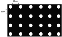
- the direct type backlight 30 has a substrate 32 and a plurality of point light sources 34 arranged two-dimensionally on the substrate 32.
- the plurality of point light sources 34 can be driven by a local dimming method, and the minimum unit of local dimming drive may be one point light source or two or more point light sources.
- the type of the point light source is not particularly limited, and examples thereof include an LED (light emitting diode) and a laser light source.
- the point light source may be a white light source, or a plurality of light sources having different emission colors may be used.
- a mini LED having a size S in FIG. 3 of 1.0 mm or less (preferably 0.6 mm or less, more preferably 0.15 mm or less) is preferable.
- the arrangement of the point light sources is preferably a grid arrangement arranged in a two-dimensional grid pattern, but may be a triangular arrangement, a hexagonal arrangement, or the like.
- the "lattice arrangement arranged in a two-dimensional lattice” is a multi-row arrangement in which light source sequences in which a plurality of point light sources are arranged at a constant pitch in one direction intersect in one direction. It means the arrangement in which the point light source is located at the grid point of the two-dimensional lattice.
- the lattice becomes a square, and the pitch of the point light source in the light source row and the light source row If the placement pitch is different, the grid will be rectangular.
- the lattice becomes a parallelogram.
- the point light sources are preferably arranged regularly, but may be arranged irregularly.
- the distance P between the closest point light sources is preferably 2 to 20 mm. In the case of regular arrangement, the distance between the point light sources means the arrangement pitch.
- the type of substrate on which the point light source is arranged is not particularly limited, but a reflector is preferable.
- the reflector include a white PET (polyethylene terephthalate) and a reflector having a reflective surface made of a multilayer film using a polyester resin.
- optical control member included in the liquid crystal display device of the present invention is not particularly limited as long as the above-mentioned requirements of the formulas (1) to (3) are satisfied, but the following aspects 1 to 3 are preferable.
- Aspect 1 First optically anisotropic layer satisfying the relationship of the formulas (4) to (6) described later
- Aspect 2 A light absorption anisotropic layer containing a dichroic substance, which is a light absorption anisotropic layer.
- a louver layer in which light-transmitting bands and light-shielding bands are alternately and repeatedly arranged.
- Examples of the optical control member include a first optically anisotropic layer satisfying the relationships of the formulas (4) to (6).
- Equation (4) 0 nm ⁇ Re1 (550) ⁇ 300 nm Equation (5) 100 nm ⁇
- ⁇ 1.2 Re1 (550) represents the in-plane retardation of the first optically anisotropic layer at a wavelength of 550 nm.
- Rth1 (550) represents the retardation in the thickness direction of the first optically anisotropic layer at a wavelength of 550 nm.
- Nz represents the Nz factor of the first optically anisotropic layer.
- the composition of the first optically anisotropic layer is not particularly limited as long as it satisfies the above optical characteristics, and is formed by using, for example, a polymer film (particularly, a stretched polymer film) and a liquid crystal compound.
- a polymer film particularly, a stretched polymer film
- a liquid crystal compound particularly, a polymer film and a liquid crystal compound.
- the light control member is a light absorption anisotropic layer containing a dichroic substance, and the light absorption differs when the direction having the highest transmittance with respect to the surface of the light absorption anisotropic layer is set as the transmission axis.
- Examples thereof include a light absorption anisotropic layer in which the angle formed by the normal direction of the rectangular layer and the transmission axis is 0 to 45 °.
- the angle formed by the normal direction of the light absorption anisotropic layer and the transmission axis is more preferably 0 to 20 ° and further preferably 0 to 10 ° in that the effect of the present invention is more excellent.
- the Mueller matrix of the light absorption anisotropic layer at a wavelength of 550 nm is measured in AxoScan OPMF-1 (manufactured by Optoscience).
- the transmittance at all omnidirectional angles at each polar angle was measured while changing the polar angle, which is the angle of the light absorption anisotropic layer with respect to the normal direction, from 0 to 90 ° in 5 ° increments.
- the direction in which the transmittance becomes the largest is defined as the transmission axis.
- the angle formed by the major axis of the dichroic substance and the thickness direction of the light absorption anisotropic layer is 0 to 45 ° ( It is preferable to adjust the temperature so that it is 0 to 20 °). Above all, it is preferable to vertically orient the dichroic substance in the light absorption anisotropic layer. In other words, it is preferable to orient the dichroic substance so that the long axis direction of the dichroic substance is substantially parallel to the thickness direction of the anisotropic light absorption layer. "Approximately parallel" means that the angle between the long axis direction of the dichroic substance and the thickness direction of the anisotropic light absorption layer is 0 to 45 °.
- the degree of orientation of the light absorption anisotropic layer at a wavelength of 550 nm is not particularly limited, but 0.80 or more is preferable, 0.90 or more is more preferable, and 0.95 or more is further preferable, in that the effect of the present invention is more excellent. ..
- the upper limit is 1.00.
- the degree of orientation is calculated by the following method. First, in AxoScan OPMF-1 (manufactured by Optoscience), the Mueller matrix of the light absorption anisotropic layer at a wavelength of 550 nm is measured at a polar angle of ⁇ 70 ° to 70 ° every 5 °.
- ko [ ⁇ ] and ke [ ⁇ ] are calculated by fitting to the following theoretical formulas in consideration of Snell's formula and Fresnel's formula.
- k -log (T) ⁇ ⁇ / (4 ⁇ d)
- the absorbance and the two-color ratio in the in-plane direction and the thickness direction are calculated, and finally the degree of orientation is obtained.
- the transmittance of the light absorption anisotropic layer at a wavelength of 550 nm in the front direction is preferably 70% or more, more preferably 80% or more.
- the upper limit is not particularly limited, but it is often 90% or less.
- the transmittance at a wavelength of 550 nm in a direction inclined by 30 ° from the transmission axis is preferably 60% or less, more preferably 40% or less, still more preferably 30% or less.
- the transmittance of the above-mentioned light absorption anisotropic layer can be appropriately adjusted depending on the concentration of the dichroic substance, the thickness of the light absorption anisotropic layer, and the like.
- the light absorption anisotropic layer is preferably formed by using a composition containing a dichroic substance and a liquid crystal compound.
- the dichroic substance is a substance having different properties between the absorbance in the major axis direction and the absorbance in the minor axis direction. Examples of the dichroic substance include a rod-shaped dichroic substance and a disk-shaped dichroic substance depending on its molecular shape, and a rod-shaped dichroic substance is preferable.
- the maximum absorption wavelength of the dichroic substance is preferably 400 to 500 nm, more preferably 440 to 480 nm.
- the dichroic substance examples include an acridine dye, an oxazine dye, a cyanine dye, a naphthalene dye, an azo dye, and an anthraquinone dye, and the azo dye is preferable.
- the azo dye examples include a monoazo dye, a bisazo dye, a trisazo dye, a tetrakisazo dye, and a stilbene azo dye, and a bisazo dye or a trisazo dye is preferable. Further, the compound described in JP-A-2018-053167 is also preferable.
- the dichroic substance may have a polymerizable group. Since the dichroic substance has a polymerizable group, the degree of cross-linking of the anisotropic light absorbing layer does not decrease even when the amount of the dichroic substance used is large, and even if it is thin, it exhibits high selective wavelength absorption and is durable. An anisotropic light absorption layer having excellent properties can be formed.
- an ethylenically unsaturated bond such as a vinyl group, a vinyloxy group, a styryl group, a p- (2-phenylethenyl) phenyl group, an acryloyl group, a methacryloyl group, an acryloyloxy group, and a methacryloyloxy group can be used.
- examples thereof include a polymerizable group, an epoxy group, and an oxetanyl group having.
- the dichroic material preferably has an aromatic ring.
- the aromatic ring include an aromatic hydrocarbon ring and an aromatic heterocycle, and among them, an aromatic hydrocarbon ring is preferable, and a benzene ring is more preferable.
- the liquid crystal compound preferably has a polymerizable group. That is, the composition preferably contains a polymerizable liquid crystal compound (a liquid crystal compound having a polymerizable group).
- the definition of the polymerizable group is as described in the section on dichroic substances.
- the liquid crystal compound preferably has an aromatic ring. Examples of the aromatic ring include an aromatic hydrocarbon ring and an aromatic heterocycle, and among them, an aromatic hydrocarbon ring is preferable, and a benzene ring is more preferable.
- the polymerizable liquid crystal compound examples include a low molecular weight liquid crystal compound having a polymerizable group and a high molecular weight liquid crystal compound having a polymerizable group.
- the "low molecular weight liquid crystal compound” means a liquid crystal compound having no repeating unit in the chemical structure.
- the "polymer liquid crystal compound” means a liquid crystal compound having a repeating unit in the chemical structure.
- the small molecule liquid crystal compound include the compounds described in JP2013-228706A.
- the polymer liquid crystal compound examples include a thermotropic liquid crystal polymer described in JP-A-2011-237513 and a side chain type liquid crystal compound described in JP-A-2015-107492. ..
- Low-molecular-weight liquid crystal compounds can be roughly classified into rod-shaped liquid crystal compounds and disc-shaped liquid crystal compounds according to their molecular shape.
- a rod-shaped liquid crystal compound is preferable.
- the polymer liquid crystal compound can be roughly classified into a main chain type liquid crystal compound and a side chain type liquid crystal compound, and the main chain type liquid crystal compound is a compound having a structure showing liquidity in the polymer main chain.
- the side-chain type liquid crystal compound is a compound having a structure showing liquidity in the polymer side chain portion.
- Side-chain liquid crystal compounds are preferable because the obtained anisotropic light absorbing layer has a high degree of orientation order and is excellent in solubility in a solvent when preparing a composition.
- the composition may contain other components other than the dichroic substance and the liquid crystal compound.
- the composition preferably contains a vertical alignment agent.
- the orientation of the dichroic substance and the liquid crystal compound can be made more vertical, and the degree of orientation order can be made higher.
- the vertical alignment agent include a boronic acid compound and an onium salt.
- Other components include leveling agents, polymerization initiators, and solvents.
- the method for forming the anisotropic light absorbing layer using the above-mentioned composition is not particularly limited, and is also referred to as a step of applying the above composition on a predetermined substrate to form a coating film (hereinafter, also referred to as a “coating film forming step”). ), The step of aligning the liquid crystal component contained in the coating film (hereinafter, also referred to as “alignment step”), and the step of applying a curing treatment to the coating film (hereinafter, also referred to as “curing step”). The method of including in order is mentioned. Hereinafter, each of the above steps will be described in detail.
- the coating film forming step is a step of applying a composition on a predetermined substrate to form a coating film.
- the type of the base material is not particularly limited, and examples thereof include a transparent support and a laminated body having an alignment film arranged on the transparent support.
- the method for applying the composition is not particularly limited, and examples thereof include known methods.
- the alignment step is a step of aligning the liquid crystal component contained in the coating film.
- the alignment step may have a drying process. By the drying treatment, components such as a solvent can be removed from the coating film.
- the orientation step preferably has a heat treatment. This makes it possible to orient the liquid crystal component contained in the coating film.
- the alignment step may have a cooling treatment performed after the heat treatment.
- the curing step is carried out, for example, by heating and / or light irradiation (exposure). Among these, it is preferable that the curing step is carried out by light irradiation.
- the light control member examples include a louver layer in which light transmission bands and light shielding bands are alternately and repeatedly arranged.
- the louver layer 40 the light transmission band 42 and the light shielding band 44 are alternately arranged.
- the first transparent protective layer 46 is laminated on one surface of the louver layer 40, and the second transparent protective layer 48 is laminated on the other surface.
- FIG. 6 is a cross-sectional view taken along the line II-II in FIG.
- the liquid crystal display device may or may not include a louver layer, and the first transparent protective layer 46 and the second transparent protective layer 48 may or may not be included.
- the light transmission band 42 and the light shielding band 44 constituting the louver layer 40 are used.
- Each has a band shape extending in the X direction, and a plurality of light transmission bands 42 and a plurality of light shielding bands 44 are alternately arranged in the Y direction.
- the width of the plurality of light transmission bands 42 in the Y direction is uniform and constant in the X direction. Further, the widths of the plurality of light-shielding bands 44 in the Y direction are also uniform and constant in the X direction.
- the material of the light transmission band 42 a resin having high transparency and low birefringence of transmitted light is used. From the viewpoint of transparency, high transparency is achieved such that the light transmittance when light is transmitted in the Z direction in the figure is 75% or more, preferably 85% or more, with respect to only the light transmission band 42.
- the resin material to have is preferable.
- specific examples of the resin having high transparency and small compound refraction include silicone resin, polycarbonate resin, polyolefin resin (particularly cycloolefin polymer), cellulose resin, and acrylic resin. Of these, silicone resin is preferable, and silicone rubber is more preferable because it has good heat resistance.
- the value of the above "light transmittance" is applied to the optical path of the inspection light in a device that uses D65 specified in JIS Z 8720 as a light source and measures the intensity of the inspection light emitted from the light source with a light receiving sensor.
- the output value of the light receiving sensor when there is no object to be measured is A
- the output value when the object to be measured is set on the optical path of the inspection light and the transmitted light transmitted through the object to be measured is received by the light source sensor is B.
- the value obtained by light transmittance (B / A) ⁇ 100 (unit;%).
- the material of the light-shielding band 44 a colored resin obtained by using the resin listed above as the material of the light-transmitting band 42 as a base material and adding a colorant such as a pigment and a dye to the base material is preferably used.
- the color tone of the light-shielding band 44 may be such that preferable light-shielding properties of the light-shielding band 44 can be obtained, and examples thereof include black, red, yellow, green, blue, and light blue.
- the color tone of the light-shielding band 44 can be adjusted by the type and amount of the colorant added.
- the colorant include general organic pigments or inorganic pigments such as carbon black, Benkara, iron oxide, titanium oxide, yellow iron oxide, disazo yellow, and phthalocyanine blue.
- the colorant may be used alone or in combination of two or more.
- a black pigment is not used, it is preferable to use a white pigment in combination in order to obtain good light-shielding properties.
- the resin material forming the light transmission band 42 and the resin material as the base material of the light shielding band 44 may be the same or different, but the light transmission band 42 and the light shielding band From the viewpoint of adhesiveness with 44, it is preferable that both are the same.
- the viewing angle ⁇ in the plane perpendicular to the X direction is determined by the thickness of the light transmission band 42 in the Z direction and the width in the Y direction. Further, the ratio of the width of the light transmitting band 42 to the width of the shading band 44 in the Y direction affects the transmittance of light rays parallel to the Z direction.
- the viewing angle ⁇ in the louver layer 40 is preferably 30 to 150 °, more preferably 60 to 120 °.
- the thickness T of the light transmission band 42 in the Z direction is preferably 50 to 200 ⁇ m, more preferably 100 to 200 ⁇ m.
- the width W1 of the light transmission band 42 in the Y direction is preferably 30 to 300 ⁇ m, more preferably 50 to 200 ⁇ m.
- the width W2 of the light-shielding band 44 in the Y direction is preferably 5 to 30 ⁇ m, more preferably 10 to 20 ⁇ m.
- the preferable range of the thickness T of the light-shielding band 44 in the Z direction is the same as the preferable range of the thickness T of the light transmission band 42.
- the material of the first transparent protective layer 46 and the second transparent protective layer 48 a resin having high transparency is used, and a resin having a small variation in birefringence in the plane is preferable. From the viewpoint of transparency, the light transmittance of each of the first transparent protective layer 46 and the second transparent protective layer 48 when light is transmitted in the Z direction in the figure is 75% or more. Is preferable, and 85% or more is more preferable.
- Specific examples of the resin having high transparency and small variation in the double refractive index in the plane in the state of being molded into a film include a polycarbonate resin, a polyolefin resin (particularly, a cycloolefin polymer), a cellulose resin, or a resin.
- the thickness of the first transparent protective layer 46 and the second transparent protective layer 48 is preferably 0.01 to 0.2 mm, more preferably 0.01 to 0.1 mm.
- the first transparent protective layer 46 and the second transparent protective layer 48 may be made of the same material, or may be made of different materials from each other. Further, the thickness of both may be the same or different. It is preferable that the first transparent protective layer 46 and the second transparent protective layer 48 are adhesively integrated with the louver layer 40 via an adhesive layer (not shown).
- the manufacturing method of the louver layer is not particularly limited, and examples thereof include the manufacturing method described in JP-A-2007-08142.
- the present invention is not limited to this mode, and the light transmission band and the light shielding band are inclined with respect to the thickness direction. There may be.
- the embodiment in which the light transmission band and the light shielding band have a certain width in the thick direction is described, but the present invention is not limited to this embodiment, and the width becomes narrower or wider as it goes in one direction. May be good.
- the structures of the light transmission band and the light shielding band can be adjusted as appropriate.
- the liquid crystal display device may have a member other than the above-mentioned member.
- the effects of the present invention are more excellent, and the formulas (7) to (8) are placed in at least one of the space between the first polarizing element and the liquid crystal cell and between the second polarizing element and the liquid crystal cell. It is preferable to have a second optically anisotropic layer including a positive A plate satisfying the relationship of) and a positive C plate satisfying the relationship of the formulas (9) to (10).
- ReA (550) represents the retardation of the positive A plate at a wavelength of 550 nm.
- ReA (450) represents the retardation of the positive A plate at a wavelength of 450 nm.
- RthC (550) represents the thickness direction retardation of the positive C plate at a wavelength of 550 nm.
- RthC (450) represents the thickness direction retardation of the positive C plate at a wavelength of 450 nm.
- the positive A plate preferably satisfies the relationship of the formulas (7A) to (8A) in that the effect of the present invention is more excellent.
- the positive C plate preferably satisfies the relationship of the formulas (9A) to (10A) in that the effect of the present invention is more excellent.
- the composition of the second optically anisotropic layer is not particularly limited as long as it satisfies the above optical characteristics, and is formed by using, for example, a polymer film (particularly, a stretched polymer film) and a liquid crystal compound.
- a polymer film particularly, a stretched polymer film
- a liquid crystal compound particularly, a polymer film (particularly, a stretched polymer film) and a liquid crystal compound. The film is mentioned.
- the liquid crystal display device has a third optical anisotropy that satisfies the relationship of the equations (11) to (12) in at least one of the space between the first polarizing element and the liquid crystal cell and the space between the second polarizing element and the liquid crystal cell. It is preferable to have a sex layer.
- Equation (11) 200 nm ⁇ Re3 (550) ⁇ 400 nm Equation (12) 0 nm ⁇
- Rth3 (550) represents the retardation in the thickness direction of the third optically anisotropic layer at a wavelength of 550 nm.
- represents the absolute value of Rth3 (550).
- the third optically anisotropic layer preferably satisfies the formulas (11A) to (12A) in that the effect of the present invention is more excellent. Equation (11A) 250 nm ⁇ Re3 (550) ⁇ 350 nm Equation (12A) 0 nm ⁇
- the composition of the third optically anisotropic layer is not particularly limited as long as it satisfies the above optical characteristics, and is formed by using, for example, a polymer film (particularly, a stretched polymer film) and a liquid crystal compound.
- a polymer film particularly, a stretched polymer film
- a liquid crystal compound particularly, a polymer film (particularly, a stretched polymer film) and a liquid crystal compound. The film is mentioned.
- the liquid crystal display device may have a light diffusing plate.
- the light diffusing plate is preferably arranged between the light control member and the direct type backlight.
- the light diffusing plate is a plate for disturbing the traveling direction of the incident light so that light having uniform brightness can be emitted from the main surface (plate surface).
- a known light diffusing plate can be used as the light diffusing plate.
- the liquid crystal display device may have a luminance improving film.
- the luminance improving film is preferably arranged between the optical control member and the direct type backlight. It is preferable that the brightness improving film is arranged on the visual recognition side (the side opposite to the direct type backlight) with respect to the light diffusing plate.
- Examples of the luminance improving film include a reflective polarizing film.
- the reflective polarizing film has a function of separating linear polarization, for example, it is arranged between the second polarizing element and the direct backlight, and the linear polarization is backscattered or backscattered to the direct backlight side.
- Examples of the multi-layered luminance improving film using the principle of the dielectric mirror include DBEF-E, DBEF-D, DBEF-M, and DBEF-P2 (all manufactured by 3M).
- Example 1 By biaxially stretching Arton (manufactured by JSR), an optically anisotropic film 1 having Re (550) of 100 nm, Rth (550) of -300 nm, and an Nz factor of -2.5 was produced. did. After that, the second polarization arranged on the back light side of ProArt PA32UCX manufactured by ASUS, which has a first polarizing element, a liquid crystal cell, a second polarizing element, a brightness improving film, a light diffusing plate, and a direct type backlight in this order.
- the above-mentioned optically anisotropic film 1 is attached to the child via an adhesive, and the above is applied between the second polarizing element and the direct type backlight (also applicable between the second polarizing element and the brightness improving film).
- the liquid crystal display device of Example 1 was produced by arranging the optically anisotropic film 1.
- the direct type backlight was equipped with a plurality of mini LEDs as point light sources.
- Example 2 (Formation of alignment film)
- TAC substrate having a thickness of 40 ⁇ m; TG40 FUJIFILM Corporation
- a composition for forming an alignment film was applied thereto with a wire bar.
- the support on which the coating film was formed was dried with warm air at 60 ° C. for 60 seconds and further dried with warm air at 100 ° C. for 120 seconds to form an alignment film, and a TAC film with an alignment film was obtained.
- the film thickness of the alignment film was 1 ⁇ m.
- composition for forming an alignment film ⁇ ⁇ Modified polyvinyl alcohol PVA-1 3.80 parts by mass ⁇ IRGACURE2959 0.20 parts by mass ⁇ 70 parts by mass of water ⁇ 30 parts by mass of methanol ⁇ ⁇
- the following composition for forming a light absorption anisotropic layer is continuously applied onto the obtained alignment film with a wire bar, and the obtained coating film is heated at 120 ° C. for 60 seconds and then at room temperature (23 ° C.). It was cooled until it became. Then, the support on which the coating film was formed was heated at 80 ° C. for 60 seconds and cooled again to room temperature. Then, the obtained coating film was irradiated with an LED lamp (center wavelength 365 nm) for 2 seconds under an irradiation condition of an illuminance of 200 mW / cm 2 , to prepare a light absorption anisotropic layer on the alignment film. ..
- the film thickness of the light absorption anisotropic layer was 3.0 ⁇ m.
- the transmittance of the light absorption anisotropic layer at a wavelength of 550 nm was 80%, and the degree of orientation was 0.97. Further, the angle formed by the transmission axis of the above-mentioned optically anisotropic layer and the normal direction of the light absorption anisotropic layer was 0 °.
- the following composition for forming a color adjusting layer was continuously applied on the obtained light absorption anisotropic layer with a wire bar to form a coating film.
- the support on which the coating film was formed was dried with warm air at 60 ° C. for 60 seconds and further dried with warm air at 100 ° C. for 120 seconds to form a color adjustment layer to form an optical film.
- the film thickness of the color adjustment layer was 0.5 ⁇ m.
- composition for forming a color adjusting layer ⁇ ⁇ Modified polyvinyl alcohol PVA-1 3.80 parts by mass ⁇ IRGACURE2959 0.20 parts by mass ⁇ Dye compound G-1 0.08 parts by mass ⁇ 70 parts by mass of water ⁇ 30 parts by mass of methanol ⁇ ⁇
- the above optical film is attached to a second polarizing element arranged on the backlight side of ProArt PA32UCX manufactured by ASUS, which has a first polarizing element, a liquid crystal cell, a second polarizing element, and a direct type backlight in this order.
- the optical film is formed.
- a liquid crystal display device was manufactured.
- Example 3 The optical difference produced in Example 1 was applied to the second polarizing element arranged on the backlight side of ProArt PA32UCX manufactured by ASUS, which has a first polarizing element, a liquid crystal cell, a second polarizing element, and a direct type backlight in this order.
- the optical film containing the light absorption anisotropic layer prepared in the square film 1 and the second embodiment is bonded to each other via an adhesive, and is placed between the second polarizing element and the direct type backlight (with the second polarizing element).
- the liquid crystal display device of Example 3 was produced by arranging the optically anisotropic film 1 and the optical film in the space between the brightness improving film and the liquid crystal display device.
- the width W2 of the light-shielding band shown in FIG. 6 is 15 ⁇ m
- the width of the light-transmitting band W1 is 70 ⁇ m
- the thickness T of the light-shielding band and the light-transmitting band is 150 ⁇ m.
- a louver layer in which a light transmission band and a light shielding band are alternately and repeatedly arranged was produced.
- a liquid crystal display device was produced according to the same procedure as in Example 1 except that the louver layer was used instead of the optically anisotropic film.
- the louver layer was arranged so that the absorption axis of the second polarizing element and the direction in which the light transmission band of the louver layer extends were orthogonal to each other.
- Example 6 An optically anisotropic film 3 having Re (550) of 280 nm and
- Example 7 The optically anisotropic film 2 was arranged between the first polarizing element in the liquid crystal display device manufactured in Example 4 and the liquid crystal cell to manufacture a liquid crystal display device.
- the optically anisotropic film 2 was arranged so that the slow axis of the optically anisotropic film 2 and the absorption axis of the first polarizing element were parallel to each other.
- Example 8> The optically anisotropic film 3 was arranged between the second polarizing element and the liquid crystal cell in the liquid crystal display device produced in Example 4, to produce a liquid crystal display device.
- the optically anisotropic film 3 was arranged so that the slow axis of the optically anisotropic film 3 and the absorption axis of the second substituent were orthogonal to each other.
- the width of the light-shielding band W2 shown in FIG. 6 is 30 ⁇ m
- the width of the light-transmitting band W1 is 20 ⁇ m
- the thickness T of the light-shielding band and the light-transmitting band is 300 ⁇ m.
- a louver layer in which a light transmission band and a light shielding band are alternately and repeatedly arranged was produced.
- a liquid crystal display device was produced according to the same procedure as in Example 1 except that the louver layer was used instead of the optically anisotropic film.
- the louver layer was arranged so that the absorption axis of the second polarizing element and the direction in which the light transmission band of the louver layer extends were orthogonal to each other.
- the liquid crystal display device is displayed in white in a dark room, and a measuring device (EZ-Contrast XL88, manufactured by ELDIM) is used to display the liquid crystal display at a predetermined polar position and azimuth position. It was obtained by measuring the white brightness. More specifically, the liquid crystal display device is displayed in white in a dark room, the polar angle is 0 ° ( ⁇ in FIG. 2 is 0 °), and the azimuth angle is 0 ° ( ⁇ in FIG. 2 is 0 °).
- I0 was obtained by arranging a measuring device at the position of and measuring the brightness.
- I20 first, the liquid crystal display device is displayed in white in a dark room, and the polar angle is 20 ° ( ⁇ in FIG. 2 is 20 °) and the azimuth angle is 45 ° ( ⁇ in FIG. 2 is 45 °).
- a measuring machine is placed at the position to obtain the brightness (brightness 20A), and the measuring machine is located at a polar angle of 20 ° ( ⁇ in FIG. 2 is 20 °) and an azimuth of 135 ° ( ⁇ is 135 ° in FIG. 2).
- the measuring instrument is placed at a position where the polar angle is 20 ° ( ⁇ in FIG.
- luminance 20A, luminance 20B, luminance 20C, luminance 20D were arithmetically averaged, and the average luminance was obtained and used as I20.
- the liquid crystal display device is displayed in white in a dark room, and the polar angle is 40 ° ( ⁇ in FIG. 2 is 40 °) and the azimuth angle is 45 ° ( ⁇ in FIG. 2 is 45 °).
- a measuring machine is placed at the position to obtain the brightness (brightness 40A), and the measuring machine is located at a polar angle of 40 ° ( ⁇ in FIG. 2 is 40 °) and an azimuth angle of 135 ° ( ⁇ is 135 ° in FIG. 2).
- the measuring instrument is placed at a position where the polar angle is 40 ° ( ⁇ in FIG.
- luminance 40A, luminance 40B, luminance 40C, luminance 40D were arithmetically averaged to obtain the average luminance, which was designated as I40.
- the liquid crystal display device is displayed in white in a dark room, and the polar angle is 60 ° ( ⁇ in FIG. 2 is 60 °) and the azimuth angle is 45 ° ( ⁇ in FIG. 2 is 45 °).
- a measuring machine is placed at the position to obtain the brightness (brightness 60A), and the measuring machine is located at a polar angle of 60 ° ( ⁇ in FIG. 2 is 60 °) and an azimuth of 135 ° ( ⁇ is 135 ° in FIG. 2).
- Is placed to obtain the brightness (brightness 60B) and the measuring instrument is placed at a position where the polar angle is 60 ° ( ⁇ in FIG.
- luminance 60A, luminance 60B, luminance 60C, luminance 60D were arithmetically averaged to obtain the average luminance, which was designated as I60.
- the liquid crystal display device of the present invention shows a desired effect. From the comparison between Examples 3 and 5 and 6, it was confirmed that a better effect can be obtained when the second optically anisotropic layer or the third optically anisotropic layer is used. From the comparison of Examples 1, 2 and 3, it was confirmed that a better effect can be obtained when the louver layer is used. From the comparison of Examples 1 to 3, it was confirmed that more excellent effects can be obtained when both the first optically anisotropic layer and the light absorption anisotropic layer are used.
- Liquid crystal display 12 1st liquid crystal display 14 Liquid crystal cell 16 2nd polarizing element 18 Optical control member 20, 30 Direct type backlight 22 Upper board 24 Lower board 26 Liquid crystal layer 32 Board 34 Point light source 40 Louver layer 42 Light transmission band 44 Light-shielding band 46 First transparent protective layer 48 Second transparent protective layer
Landscapes
- Physics & Mathematics (AREA)
- Nonlinear Science (AREA)
- General Physics & Mathematics (AREA)
- Optics & Photonics (AREA)
- Chemical & Material Sciences (AREA)
- Crystallography & Structural Chemistry (AREA)
- Mathematical Physics (AREA)
- Liquid Crystal (AREA)
- Optical Elements Other Than Lenses (AREA)
- Polarising Elements (AREA)
Priority Applications (3)
| Application Number | Priority Date | Filing Date | Title |
|---|---|---|---|
| CN202180061556.XA CN116057424B (zh) | 2020-09-11 | 2021-09-06 | 液晶显示装置 |
| JP2022547583A JP7404552B2 (ja) | 2020-09-11 | 2021-09-06 | 液晶表示装置 |
| US18/180,598 US11860480B2 (en) | 2020-09-11 | 2023-03-08 | Liquid crystal display device |
Applications Claiming Priority (2)
| Application Number | Priority Date | Filing Date | Title |
|---|---|---|---|
| JP2020152570 | 2020-09-11 | ||
| JP2020-152570 | 2020-09-11 |
Related Child Applications (1)
| Application Number | Title | Priority Date | Filing Date |
|---|---|---|---|
| US18/180,598 Continuation US11860480B2 (en) | 2020-09-11 | 2023-03-08 | Liquid crystal display device |
Publications (1)
| Publication Number | Publication Date |
|---|---|
| WO2022054757A1 true WO2022054757A1 (ja) | 2022-03-17 |
Family
ID=80631833
Family Applications (1)
| Application Number | Title | Priority Date | Filing Date |
|---|---|---|---|
| PCT/JP2021/032655 Ceased WO2022054757A1 (ja) | 2020-09-11 | 2021-09-06 | 液晶表示装置 |
Country Status (4)
| Country | Link |
|---|---|
| US (1) | US11860480B2 (https=) |
| JP (1) | JP7404552B2 (https=) |
| CN (1) | CN116057424B (https=) |
| WO (1) | WO2022054757A1 (https=) |
Families Citing this family (1)
| Publication number | Priority date | Publication date | Assignee | Title |
|---|---|---|---|---|
| US20230244107A1 (en) * | 2022-02-01 | 2023-08-03 | 3M Innovative Properties Company | Optical film stack for direct backlight unit |
Citations (5)
| Publication number | Priority date | Publication date | Assignee | Title |
|---|---|---|---|---|
| WO2006001448A1 (ja) * | 2004-06-29 | 2006-01-05 | Sharp Kabushiki Kaisha | 位相差フィルム、偏光フィルム、液晶表示装置、及び、位相差フィルムの設計方法 |
| JP2011197409A (ja) * | 2010-03-19 | 2011-10-06 | Nippon Shokubai Co Ltd | 位相差フィルムとその製造方法および画像表示装置 |
| WO2014034481A1 (ja) * | 2012-08-27 | 2014-03-06 | シャープ株式会社 | 液晶表示装置 |
| WO2017022800A1 (ja) * | 2015-08-04 | 2017-02-09 | シャープ株式会社 | 配光制御部材、照明装置および液晶表示装置 |
| WO2019045098A1 (ja) * | 2017-09-04 | 2019-03-07 | 富士フイルム株式会社 | 機能性フィルム、面光源装置および液晶表示装置 |
Family Cites Families (7)
| Publication number | Priority date | Publication date | Assignee | Title |
|---|---|---|---|---|
| JP2000111857A (ja) * | 1998-10-05 | 2000-04-21 | Matsushita Electric Ind Co Ltd | 液晶表示装置の評価方法 |
| US7527408B2 (en) | 2005-10-24 | 2009-05-05 | Lg Electronics Inc. | Backlight unit having heat dissipating layer, display device having heat dissipating layer, and method for manufacturing heat dissipating layer |
| JP5186164B2 (ja) * | 2006-12-21 | 2013-04-17 | 富士フイルム株式会社 | 液晶表示装置 |
| JP2015175994A (ja) * | 2014-03-14 | 2015-10-05 | 大日本印刷株式会社 | 反射防止フィルム及び画像表示装置 |
| JP2015202917A (ja) * | 2014-04-11 | 2015-11-16 | 株式会社日立製作所 | エレベータ装置 |
| JP6645420B2 (ja) * | 2014-10-30 | 2020-02-14 | 東洋紡株式会社 | 液晶表示装置及び偏光板 |
| KR102227340B1 (ko) * | 2017-05-08 | 2021-03-11 | 후지필름 가부시키가이샤 | 액정 표시 장치 |
-
2021
- 2021-09-06 CN CN202180061556.XA patent/CN116057424B/zh active Active
- 2021-09-06 WO PCT/JP2021/032655 patent/WO2022054757A1/ja not_active Ceased
- 2021-09-06 JP JP2022547583A patent/JP7404552B2/ja active Active
-
2023
- 2023-03-08 US US18/180,598 patent/US11860480B2/en active Active
Patent Citations (5)
| Publication number | Priority date | Publication date | Assignee | Title |
|---|---|---|---|---|
| WO2006001448A1 (ja) * | 2004-06-29 | 2006-01-05 | Sharp Kabushiki Kaisha | 位相差フィルム、偏光フィルム、液晶表示装置、及び、位相差フィルムの設計方法 |
| JP2011197409A (ja) * | 2010-03-19 | 2011-10-06 | Nippon Shokubai Co Ltd | 位相差フィルムとその製造方法および画像表示装置 |
| WO2014034481A1 (ja) * | 2012-08-27 | 2014-03-06 | シャープ株式会社 | 液晶表示装置 |
| WO2017022800A1 (ja) * | 2015-08-04 | 2017-02-09 | シャープ株式会社 | 配光制御部材、照明装置および液晶表示装置 |
| WO2019045098A1 (ja) * | 2017-09-04 | 2019-03-07 | 富士フイルム株式会社 | 機能性フィルム、面光源装置および液晶表示装置 |
Also Published As
| Publication number | Publication date |
|---|---|
| JP7404552B2 (ja) | 2023-12-25 |
| JPWO2022054757A1 (https=) | 2022-03-17 |
| CN116057424A (zh) | 2023-05-02 |
| US20230221600A1 (en) | 2023-07-13 |
| CN116057424B (zh) | 2025-08-01 |
| US11860480B2 (en) | 2024-01-02 |
Similar Documents
| Publication | Publication Date | Title |
|---|---|---|
| US9110242B2 (en) | Liquid crystal display, laminated polarizing plate and polarized light source device | |
| JP4931929B2 (ja) | 偏光制御システム及び表示装置 | |
| KR101891421B1 (ko) | 위상차판, 위상차판을 이용한 적층 편광판, 및 위상차판을 이용한 표시 장치 | |
| TWI529455B (zh) | 圓形偏光板及包含其之反射液晶顯示器 | |
| CN102124401A (zh) | 液晶显示装置 | |
| US11204524B2 (en) | Image display device | |
| WO2015037369A1 (ja) | 偏光板、偏光板の製造方法、画像表示装置、画像表示装置の製造方法及び偏光板の光透過率改善方法 | |
| WO2016047517A1 (ja) | 円偏光板及びその製造方法、広帯域λ/4板、有機エレクトロルミネッセンス表示装置、並びに液晶表示装置 | |
| TW201502661A (zh) | 液晶顯示裝置 | |
| US8184245B2 (en) | Optical compensation film for VA-mode liquid crystal display device and VA-mode liquid crystal display device | |
| WO2005093474A1 (ja) | 光学フィルムおよび画像表示装置 | |
| JP2005283846A (ja) | 光学フィルムおよび液晶表示装置 | |
| US11860480B2 (en) | Liquid crystal display device | |
| JP6448182B2 (ja) | 画像表示装置、偏光板複合体の製造方法、偏光板セットの製造方法、画像表示装置の製造方法及び画像表示装置の視認性改善方法 | |
| JPH11295526A5 (https=) | ||
| US20260086277A1 (en) | Optical element and display device | |
| US20250130458A1 (en) | Optical element and display device | |
| US20230314868A1 (en) | Liquid crystal display device | |
| JP2025165147A (ja) | 光学素子及び表示装置 | |
| JP2025165146A (ja) | 光学素子及び表示装置 | |
| JP2024077954A (ja) | 光学素子及び表示装置 | |
| JP2017062500A (ja) | 偏光板、偏光板の製造方法、画像表示装置、画像表示装置の製造方法及び偏光板の光透過率改善方法 | |
| JP2024077955A (ja) | 光学素子及び表示装置 | |
| TW200819799A (en) | Liquid crystal display | |
| JP2018077529A (ja) | 偏光板、偏光板の製造方法、画像表示装置、画像表示装置の製造方法及び偏光板の光透過率改善方法 |
Legal Events
| Date | Code | Title | Description |
|---|---|---|---|
| 121 | Ep: the epo has been informed by wipo that ep was designated in this application |
Ref document number: 21866716 Country of ref document: EP Kind code of ref document: A1 |
|
| ENP | Entry into the national phase |
Ref document number: 2022547583 Country of ref document: JP Kind code of ref document: A |
|
| NENP | Non-entry into the national phase |
Ref country code: DE |
|
| 122 | Ep: pct application non-entry in european phase |
Ref document number: 21866716 Country of ref document: EP Kind code of ref document: A1 |
|
| WWG | Wipo information: grant in national office |
Ref document number: 202180061556.X Country of ref document: CN |