WO2022044848A1 - パッケージ、及びその製造方法 - Google Patents
パッケージ、及びその製造方法 Download PDFInfo
- Publication number
- WO2022044848A1 WO2022044848A1 PCT/JP2021/029800 JP2021029800W WO2022044848A1 WO 2022044848 A1 WO2022044848 A1 WO 2022044848A1 JP 2021029800 W JP2021029800 W JP 2021029800W WO 2022044848 A1 WO2022044848 A1 WO 2022044848A1
- Authority
- WO
- WIPO (PCT)
- Prior art keywords
- transparent substrate
- sacrificial layer
- hole
- manufacturing
- substrate
- Prior art date
- Legal status (The legal status is an assumption and is not a legal conclusion. Google has not performed a legal analysis and makes no representation as to the accuracy of the status listed.)
- Ceased
Links
Images








































































Classifications
-
- G—PHYSICS
- G02—OPTICS
- G02B—OPTICAL ELEMENTS, SYSTEMS OR APPARATUS
- G02B3/00—Simple or compound lenses
-
- H—ELECTRICITY
- H10—SEMICONDUCTOR DEVICES; ELECTRIC SOLID-STATE DEVICES NOT OTHERWISE PROVIDED FOR
- H10F—INORGANIC SEMICONDUCTOR DEVICES SENSITIVE TO INFRARED RADIATION, LIGHT, ELECTROMAGNETIC RADIATION OF SHORTER WAVELENGTH OR CORPUSCULAR RADIATION
- H10F39/00—Integrated devices, or assemblies of multiple devices, comprising at least one element covered by group H10F30/00, e.g. radiation detectors comprising photodiode arrays
- H10F39/011—Manufacture or treatment of image sensors covered by group H10F39/12
- H10F39/024—Manufacture or treatment of image sensors covered by group H10F39/12 of coatings or optical elements
-
- H—ELECTRICITY
- H10—SEMICONDUCTOR DEVICES; ELECTRIC SOLID-STATE DEVICES NOT OTHERWISE PROVIDED FOR
- H10F—INORGANIC SEMICONDUCTOR DEVICES SENSITIVE TO INFRARED RADIATION, LIGHT, ELECTROMAGNETIC RADIATION OF SHORTER WAVELENGTH OR CORPUSCULAR RADIATION
- H10F39/00—Integrated devices, or assemblies of multiple devices, comprising at least one element covered by group H10F30/00, e.g. radiation detectors comprising photodiode arrays
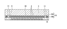
- H10F39/011—Manufacture or treatment of image sensors covered by group H10F39/12
- H10F39/026—Wafer-level processing
-
- H—ELECTRICITY
- H10—SEMICONDUCTOR DEVICES; ELECTRIC SOLID-STATE DEVICES NOT OTHERWISE PROVIDED FOR
- H10F—INORGANIC SEMICONDUCTOR DEVICES SENSITIVE TO INFRARED RADIATION, LIGHT, ELECTROMAGNETIC RADIATION OF SHORTER WAVELENGTH OR CORPUSCULAR RADIATION
- H10F39/00—Integrated devices, or assemblies of multiple devices, comprising at least one element covered by group H10F30/00, e.g. radiation detectors comprising photodiode arrays
- H10F39/10—Integrated devices
- H10F39/12—Image sensors
-
- H—ELECTRICITY
- H10—SEMICONDUCTOR DEVICES; ELECTRIC SOLID-STATE DEVICES NOT OTHERWISE PROVIDED FOR
- H10F—INORGANIC SEMICONDUCTOR DEVICES SENSITIVE TO INFRARED RADIATION, LIGHT, ELECTROMAGNETIC RADIATION OF SHORTER WAVELENGTH OR CORPUSCULAR RADIATION
- H10F39/00—Integrated devices, or assemblies of multiple devices, comprising at least one element covered by group H10F30/00, e.g. radiation detectors comprising photodiode arrays
- H10F39/80—Constructional details of image sensors
- H10F39/804—Containers or encapsulations
-
- H—ELECTRICITY
- H10—SEMICONDUCTOR DEVICES; ELECTRIC SOLID-STATE DEVICES NOT OTHERWISE PROVIDED FOR
- H10F—INORGANIC SEMICONDUCTOR DEVICES SENSITIVE TO INFRARED RADIATION, LIGHT, ELECTROMAGNETIC RADIATION OF SHORTER WAVELENGTH OR CORPUSCULAR RADIATION
- H10F39/00—Integrated devices, or assemblies of multiple devices, comprising at least one element covered by group H10F30/00, e.g. radiation detectors comprising photodiode arrays
- H10F39/80—Constructional details of image sensors
- H10F39/805—Coatings
- H10F39/8057—Optical shielding
-
- H—ELECTRICITY
- H10—SEMICONDUCTOR DEVICES; ELECTRIC SOLID-STATE DEVICES NOT OTHERWISE PROVIDED FOR
- H10F—INORGANIC SEMICONDUCTOR DEVICES SENSITIVE TO INFRARED RADIATION, LIGHT, ELECTROMAGNETIC RADIATION OF SHORTER WAVELENGTH OR CORPUSCULAR RADIATION
- H10F39/00—Integrated devices, or assemblies of multiple devices, comprising at least one element covered by group H10F30/00, e.g. radiation detectors comprising photodiode arrays
- H10F39/80—Constructional details of image sensors
- H10F39/806—Optical elements or arrangements associated with the image sensors
-
- H—ELECTRICITY
- H10—SEMICONDUCTOR DEVICES; ELECTRIC SOLID-STATE DEVICES NOT OTHERWISE PROVIDED FOR
- H10F—INORGANIC SEMICONDUCTOR DEVICES SENSITIVE TO INFRARED RADIATION, LIGHT, ELECTROMAGNETIC RADIATION OF SHORTER WAVELENGTH OR CORPUSCULAR RADIATION
- H10F39/00—Integrated devices, or assemblies of multiple devices, comprising at least one element covered by group H10F30/00, e.g. radiation detectors comprising photodiode arrays
- H10F39/80—Constructional details of image sensors
- H10F39/806—Optical elements or arrangements associated with the image sensors
- H10F39/8063—Microlenses
-
- H—ELECTRICITY
- H10—SEMICONDUCTOR DEVICES; ELECTRIC SOLID-STATE DEVICES NOT OTHERWISE PROVIDED FOR
- H10F—INORGANIC SEMICONDUCTOR DEVICES SENSITIVE TO INFRARED RADIATION, LIGHT, ELECTROMAGNETIC RADIATION OF SHORTER WAVELENGTH OR CORPUSCULAR RADIATION
- H10F39/00—Integrated devices, or assemblies of multiple devices, comprising at least one element covered by group H10F30/00, e.g. radiation detectors comprising photodiode arrays
- H10F39/80—Constructional details of image sensors
- H10F39/811—Interconnections
-
- H—ELECTRICITY
- H10—SEMICONDUCTOR DEVICES; ELECTRIC SOLID-STATE DEVICES NOT OTHERWISE PROVIDED FOR
- H10W—GENERIC PACKAGES, INTERCONNECTIONS, CONNECTORS OR OTHER CONSTRUCTIONAL DETAILS OF DEVICES COVERED BY CLASS H10
- H10W76/00—Containers; Fillings or auxiliary members therefor; Seals
- H10W76/10—Containers or parts thereof
Definitions
- This disclosure relates to a solid-state image sensor and other packages, and a method for manufacturing the same.
- the solid-state image pickup device has an element substrate in which an on-chip lens is provided on the light incident surface of a pixel to be photoelectrically converted, and the on-chip lens is sealed with respect to the element substrate.
- the transparent substrate is attached so as to stop.
- a chip size package in which a rewiring layer is provided on the back surface of the device (the back surface side of the element substrate) is also known.
- Patent Document 1 The solid-state image sensor described in Patent Document 1 is provided with a hollow portion between the on-chip lens and the transparent substrate. Further, the hollow portion communicates with the outside of the element by a through hole penetrating the transparent substrate in the thickness direction. Further, Patent Document 1 has a structure in which flare is reduced and moisture is less likely to be trapped in the hollow portion by having a hollow portion and a through hole.
- Patent Document 1 describes that when a solid-state image sensor is manufactured, a hollow portion is formed between the element substrate and the transparent substrate, and then rewiring is formed on the back surface side of the element substrate. ing.
- the element substrate and the glass substrate thinner.
- the thinner the glass substrate or the like the more easily the glass substrate or the like bends.
- the glass substrate may come into contact with the on-chip lens. Then, this contact is more likely to occur as the thickness of the hollow portion is reduced.
- the present disclosure has been made focusing on such a point, and an object thereof is to suppress the occurrence of flare and to prevent the glass substrate from coming into contact with the on-chip lens.
- a package according to an embodiment of the present disclosure includes a flattening film covering an on-chip lens formed on the light incident side of a substrate on which an element is formed, and a transparent substrate formed on the light incident side of the flattening film.
- a flattening film covering the on-chip lens formed on the light incident side of the substrate on which the element is formed is formed, and the light incident side of the flattening film is formed.
- the transparent substrate is laminated via the sacrificial layer and the adhesive layer arranged on the outer periphery of the sacrificial layer to form a through hole for communicating the sacrificial layer to the outside.
- the sacrificial layer is etched through the surface to form a hollow portion.
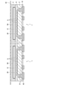
- 11 for explaining the solid-state image sensor according to the tenth aspect. It is a bottom view explaining the recess and the support part of another example which concerns on the tenth embodiment. It is a bottom view explaining the recess and the support part which concerns on eleventh embodiment. 11 is a cross-sectional view taken along the line aa of FIG. 11 for explaining the solid-state image sensor according to the eleventh embodiment. 11 is a cross-sectional view taken along the line bb of FIG. 11 for explaining the solid-state image pickup device according to the eleventh embodiment. It is a bottom view explaining the recess and the support part of another example which concerns on eleventh embodiment. It is sectional drawing explaining the solid-state image pickup device which concerns on 12th embodiment.
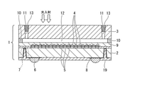
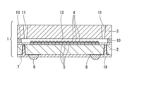
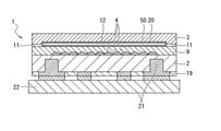
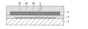
- the solid-state image pickup device of the first embodiment includes a substrate 2 on which the element is formed and a transparent substrate 3.
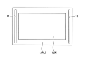
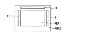
- a substrate 2 on which the element is formed has an effective pixel region ARA1 set on one surface (upper surface in FIG. 1A, hereinafter also simply referred to as an upper surface) as shown in FIG. 1B, which is a conceptual diagram.
- the outer peripheral region ARA2 is referred to as the outer peripheral region ARA2 rather than the effective pixel region ARA1.
- a plurality of on-chip lenses 4 are arranged in a two-dimensional array in the effective pixel region ARA 1 so as to correspond to each photoelectric conversion element (not shown) arranged in a two-dimensional array.
- a color filter 5 is arranged below the on-chip lens 4.
- FIG. 1A illustrates the solder ball 6 and the through silicon via 7.
- reference numeral 8 indicates a rewiring layer
- reference numeral 19 indicates a solder mask.
- the wiring on the back surface side is not limited to this structure, and other known wiring structures can also be adopted.
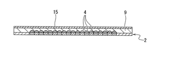
- a flattening film 9 is formed on the upper surface of the substrate 2 on which the element is formed.
- the flattening film 9 is a layer that covers the on-chip lens 4 formed on the substrate 2 on which the element is formed and flattens the upper surface of the substrate 2 on which the element is formed.
- the flattening film 9 is made of a translucent resin material.
- the flattening film 9 uses an ultraviolet curable type, a thermosetting type, or a resin having a curing reaction mechanism combined with them as its material.
- resins include acrylic, styrene, and silicone resins. Fluorine may be appropriately contained in such a resin, or hollow silica or the like may be dispersed and mixed.
- the transparent substrate 3 is a sealing material that seals the upper surface of the substrate 2 on which the element is formed.
- the transparent substrate 3 of this embodiment is made of, for example, a glass substrate.
- the transparent substrate 3 may be made of a light-transmitting material.
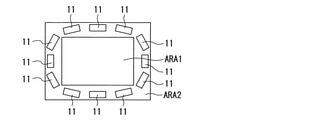
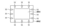
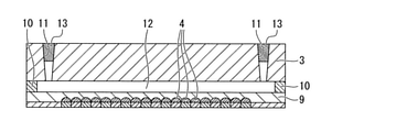
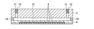
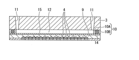
- a through hole 11 is formed in the transparent substrate 3. As shown in FIG. 1B, the through hole 11 is arranged at a position facing the outer peripheral region ARA2 of the substrate 2 on which the element is formed in a plan view.
- the plan view refers to a case where the transparent substrate 3 is viewed from a direction along the thickness direction (upper or lower in FIG. 1A).
- the through hole 11 of this embodiment extends in the thickness direction of the transparent substrate 3, for example, as shown in FIG. 1A. As shown in FIG. 1B, the through hole 11 of this embodiment has a slit-shaped opening shape.
- the transparent substrate is laminated on the flattening film 9 by being attached onto the flattening film 9 via the adhesive layer 10.
- the adhesive layer 10 is located on the outer peripheral side of the through hole 11 at a position facing the outer peripheral region ARA2 of the substrate 2 on which the element is formed in a plan view.
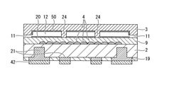
- the through hole 11 is an opening that communicates the hollow portion 12 to the outside.
- the hollow portion 12 of the present embodiment is composed of an air layer (cavity).
- the air layer is formed between the flattening film 9 and the transparent substrate 3, and is composed of a hollow body sealed with the flattening film 9, the transparent substrate 3, and the adhesive layer 10 on the outer periphery. That is, the hollow portion 12 of the present embodiment is composed of the hollow on the inner peripheral side of the adhesive layer 10.
- the hollow portion 12 is formed in a region overlapping the entire on-chip lens 4 in a plan view.
- the hollow portion 12 includes an effective pixel region ARA1 in a plan view and is a part of an outer peripheral region ARA2 thereof. It is formed so as to overlap with.
- a part of the outer peripheral region ARA2 includes a region where the through hole 11 is formed in a plan view.
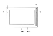
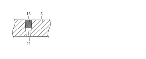
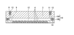
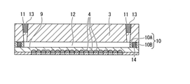
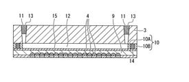
- the solid-state image pickup device 1 of the first embodiment may include a seal member 13 that closes the through hole 11 as shown in FIG. 2A.
- the seal member 13 seals the through hole 11 as shown in FIGS. 2A and 2B. That is, the seal member 13 is a member that closes the through hole 11.
- an ultraviolet curable type for example, an ultraviolet curable type, a thermosetting type, or a resin having a curing reaction mechanism combined with them is used.
- resins include epoxy-based, acrylic-based, and silicone-based resins, and modified resins of these resins.
- a black dye is added to the resin material constituting the seal member 13.
- the black dye include carbon black, titanium black, iron oxide, a composite oxide of copper and chromium, and a composite oxide of copper, chromium, and zinc.
- the dye added to the seal member 13 is not limited to the black dye, and may be another dye capable of blocking light.
- the solid-state image sensor 1 of the second embodiment will be described with reference to the drawings.
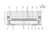
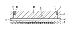
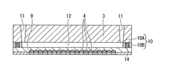
- the basic configuration of this embodiment is the same as that of the first embodiment, except that the spacer 14 is embedded in the adhesive layer 10.
- Other configurations are the same as in the first embodiment.
- the spacer 14 is formed on the lower surface of the transparent substrate 3 at a position facing the outer peripheral region ARA 2, and projects from the lower surface of the transparent substrate 3 toward the flattening film 9.
- the spacer 14 of this embodiment is formed at a position where it can be embedded in the adhesive layer 10.
- the spacer 14 may be formed so as to surround the entire outer peripheral portion of the hollow portion 12, or may be partially formed along the circumferential direction.
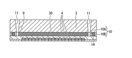
- the spacer 14 of the present embodiment is provided only at the position of the seal resin layer located on the outer side of each of the left and right through holes 11 in a plan view. Further, in this embodiment, as shown in FIG. 3, the sealing resin of the adhesive layer 10 is formed so as to be adhered to the entire circumference of the side surface of the spacer 14. That is, as shown in FIG. 3, the adhesive layer 10 has an inner peripheral side portion 10A from the spacer 14 and an outer peripheral side portion 10B from the spacer 14.
- the spacer 14 is made of the same material as the transparent substrate 3 integrally with the transparent substrate 3, for example.
- the spacer 14 may be made of a material different from that of the transparent substrate 3. For example, it may be configured to contain the same material as the sacrificial layer for forming the hollow portion 12.
- the spacer 14 is a member that secures a distance between the transparent substrate 3 and the flattening film 9 (the upper surface of the substrate 2 on which the element is formed).
- the sealing resin of the adhesive layer 10 may or may not be arranged on the lower end surface of the spacer 14.
- the solid-state image sensor 1 of the second embodiment may include a seal member 13 that closes the through hole 11 as in the first embodiment.
- the structure of the seal member 13 is the same as that of the first embodiment.
- the solid-state image sensor 1 of the third embodiment will be described with reference to the drawings.
- the basic configuration of this embodiment is the same as that of the first embodiment, except that the adhesive layer 15 is provided on the flattening film 9.
- Other configurations are the same as in the first embodiment.
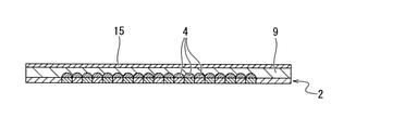
- the adhesive layer 15 is formed on the flattening film 9 as shown in FIG.
- the adhesive layer 15 is preferably made of a resin material having a lower refractive index than the flattening film 9.
- a hollow portion 12 and an adhesive layer 10 are formed on the adhesive layer 15.
- the solid-state image sensor 1 of the third embodiment may include a seal member 13 that closes the through hole 11 as in the first embodiment.
- the structure of the seal member 13 is the same as that of the first embodiment.
- the spacer 14 is formed on the lower surface of the transparent substrate 3 at a position facing the outer peripheral region ARA 2, and projects from the lower surface of the transparent substrate 3 toward the adhesive layer 10.
- the spacer 14 of this embodiment is formed at a position where it can be embedded in the adhesive layer 10.
- the spacer 14 may be formed so as to surround the entire outer peripheral portion of the hollow portion 12, or may be partially formed along the circumferential direction.
- the spacer 14 of the present embodiment is provided only at the position of the adhesive layer 10 located on the outer side of each of the left and right through holes 11 in a plan view. Further, in this embodiment, as shown in FIG. 5, the entire side surface of the spacer 14 is formed so that the sealing resin of the adhesive layer 10 is adhered to it. That is, as shown in FIG. 5, the adhesive layer 10 has an inner peripheral side portion 10A from the spacer 14 and an outer peripheral side portion 10B from the spacer 14.
- the spacer 14 is made of the same material as the transparent substrate 3 integrally with the transparent substrate 3, for example.
- the spacer 14 may be made of a material different from that of the transparent substrate 3. For example, it may be composed of the same material as the sacrificial layer for forming the hollow portion 12.
- the spacer 14 is a member that secures a distance between the transparent substrate 3 and the flattening film 9 (the upper surface of the substrate 2 on which the element is formed).
- the sealing resin of the adhesive layer 10 may or may not be arranged on the lower end surface of the spacer 14.
- the solid-state image sensor 1 of the fourth embodiment may include a seal member 13 that closes the through hole 11 as in the first embodiment.
- the structure of the seal member 13 is the same as that of the first embodiment.
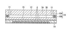
- the solid-state image sensor 1 of the fifth embodiment will be described with reference to the drawings. As shown in FIG. 6, this embodiment is different from the third embodiment in that the hollow portion 12 is formed in the transparent substrate 3. As shown in FIG. 6, the solid-state image pickup device of the fifth embodiment includes a substrate 2 on which the element is formed and a transparent substrate 3.
- FIG. 1A illustrates the solder ball 6 and the through silicon via 7.
- a flattening film 9 is formed on the upper surface of the substrate 2 on which the element is formed.
- the flattening film 9 is a layer that covers the on-chip lens 4 formed on the substrate 2 on which the element is formed and flattens the upper surface of the substrate 2 on which the element is formed.
- the adhesive layer 15 is formed on the flattening film 9 as shown in FIG.
- the adhesive layer 15 is preferably made of a resin material having a lower refractive index than the flattening film 9.
- the hollow portion 12 and the adhesive layer 10 are formed on the layer 15 of the adhesive.
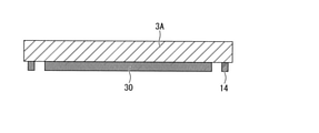
- the transparent substrate 3 of the present embodiment includes two glass substrates, and the two glass substrates are laminated via the adhesive layer 10.
- a through hole 11 is formed in the upper glass substrate 3A. As shown in FIG. 6, the through hole 11 is arranged at a position facing the outer peripheral region ARA2 of the substrate 2 on which the element is formed in a plan view. The through hole 11 extends in the thickness direction of the transparent substrate 3.
- the through hole 11 of the present embodiment has a slit-shaped opening shape, for example, as in the first embodiment. In this embodiment, the through hole 11 is not formed in the lower glass substrate 3B.
- the hollow portion 12 is sealed between the two glass substrates.
- the hollow portion 12 is composed of a cavity sealed with two glass substrates and an outer peripheral adhesive layer 10. That is, the hollow portion 12 of the present embodiment is composed of the hollow on the inner peripheral side of the adhesive layer 10.
- the hollow portion 12 is formed in a region overlapping the entire on-chip lens 4 in a plan view.
- the hollow portion 12 includes an effective pixel region ARA1 in a plan view and is a part of an outer peripheral region ARA2 thereof. It is formed so as to overlap with.
- a part of the outer peripheral region ARA2 includes a region where the through hole 11 is formed in a plan view. As a result, the hollow portion 12 can communicate with the outside through the through hole 11.
- the transparent substrate 3 may have a configuration in which three or more glass substrates are laminated. Further, the hollow portion 12 may be formed between any of the glass substrates.
- a hollow portion 12 may be separately formed between the transparent substrate 3 and the flattening film 9.
- the lower surface of the glass substrate 3B on the lower side of the transparent substrate 3 composed of the plurality of sheets is laminated on the adhesive layer 15.
- the adhesive layer 15 and the lower glass substrate 3B are interposed between the flattening film 9 and the hollow portion 12.
- the solid-state image pickup device 1 of the fifth embodiment may include a seal member 13 that closes the through hole 11 as in the first embodiment.
- the structure of the seal member 13 is the same as that of the first embodiment.
- the spacer 14 is formed on the lower surface of the upper glass substrate 3A at a position facing the outer peripheral region ARA2, and projects from the lower surface of the upper glass substrate 3A toward the lower glass substrate 3B.
- the spacer 14 of this embodiment is formed at a position where it can be embedded in the adhesive layer 10.
- the spacer 14 may be formed so as to surround the entire outer peripheral portion of the hollow portion 12, or may be partially formed along the circumferential direction.
- the spacer 14 of the present embodiment is provided only at the position of the adhesive layer 10 located on the outer side of each of the left and right through holes 11 in a plan view. Further, in this embodiment, as shown in FIG. 7, the entire side surface of the spacer 14 is formed so that the sealing resin of the adhesive layer 10 is adhered to it. That is, as shown in FIG. 7, the adhesive layer 10 has an inner peripheral side portion 10A from the spacer 14 and an outer peripheral side portion 10B from the spacer 14.
- the spacer 14 is made of the same material as the transparent substrate 3 integrally with the transparent substrate 3, for example.
- the spacer 14 may be made of a material different from that of the transparent substrate 3. For example, it may be composed of the same material as the sacrificial layer for forming the hollow portion 12.
- the spacer 14 is a member that secures a distance between the transparent substrate 3 and the flattening film 9 (the upper surface of the substrate 2 on which the element is formed).
- the sealing resin of the adhesive layer 10 may or may not be arranged on the lower end surface of the spacer 14.
- the solid-state image pickup device 1 of the sixth embodiment may include a seal member 13 that closes the through hole 11 as in the first embodiment.
- the structure of the seal member 13 is the same as that of the first embodiment.
- the solid-state image sensor 1 of the seventh embodiment will be described with reference to the drawings.
- the basic configuration of this embodiment is the same as that of the first embodiment, except that the adhesive layer 10 is also formed on the flattening film 9.
- Other configurations are the same as in the first embodiment. Therefore, the description of other configurations will be omitted.
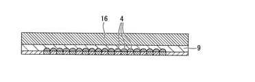
- the adhesive layer 10 formed on the upper surface of the flattening film 9 is formed in the portion formed in the effective pixel region ARA1 (the portion of reference numeral 16 in FIG. 8) and the outer peripheral region ARA2.
- the adhesive layer 10 is composed of a thick portion.
- the hollow portion 12 is composed of a space surrounded by the transparent substrate 3, the adhesive layer 16 on the bottom surface side, and the adhesive layer 10 constituting the wall portion rising in the outer peripheral region ARA 2. Similar to the sixth embodiment, the spacer 14 may be embedded in the adhesive layer 10 located in the outer peripheral region ARA2.
- the solid-state image sensor 1 of the seventh embodiment may include a seal member 13 that closes the through hole 11 as in the first embodiment.
- the structure of the seal member 13 is the same as that of the first embodiment.
- the flattening film 9 is not provided on the substrate 2 on which the element is formed.
- the eighth embodiment has a structure in which the transparent substrate 3 is directly attached to the upper surface of the substrate 2 on which the element is formed via the adhesive layer 10 and the transparent substrate 3 is laminated.
- the hollow portion 12 of the present embodiment is composed of a cavity surrounded by the upper surface of the substrate 2 on which the element is formed, the lower surface of the transparent substrate 3, and the adhesive layer 10 on the outer periphery.
- the solid-state image sensor 1 of the eighth embodiment may include a seal member 13 that closes the through hole 11 as in the first embodiment.
- the structure of the seal member 13 is the same as that of the first embodiment.
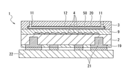
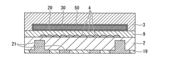
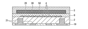
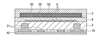
- the solid-state image pickup device of the ninth embodiment includes a substrate 2 on which the element is formed and a transparent substrate 3.
- reference numeral 19 indicates a solder mask
- reference numeral 22 indicates a mounting board connected to the wiring on the back surface side.
- a plurality of on-chip lenses 4 are arranged in a two-dimensional array shape corresponding to each photoelectric conversion element (not shown) arranged in a two-dimensional array shape with respect to the effective pixel region ARA1.
- RDL / solder balls 6 and other wirings are formed on the back surface side of the substrate 2 on which the elements are formed.
- a flattening film 9 is formed on the upper surface of the substrate 2 on which the element is formed.
- the flattening film 9 is a layer that covers the on-chip lens 4 formed on the substrate 2 on which the element is formed and flattens the upper surface of the substrate 2 on which the element is formed.
- the transparent substrate 3 is a sealing material that seals the upper surface of the substrate 2 on which the element is formed.
- the transparent substrate 3 of this embodiment is made of a glass substrate.
- the transparent substrate 3 may be made of a light-transmitting material.
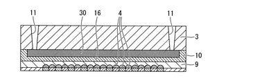
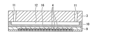
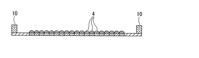
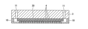
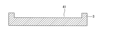
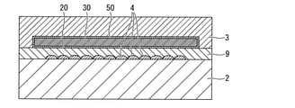
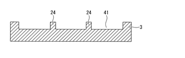
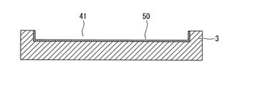
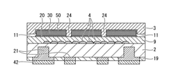
- ⁇ Hollow part 12> A recess is formed on the lower surface of the transparent substrate 3. The recess and the cavity surrounded by the flattening film 9 form the hollow portion 12.
- the hollow portion 12 is formed in a region overlapping the entire on-chip lens 4 in a plan view.
- the hollow portion 12 includes an effective pixel region ARA1 in a plan view and is one of the outer peripheral regions ARA2 thereof. It is formed so as to overlap the part.
- a part of the outer peripheral region ARA2 includes a region where the through hole 11 is formed in a plan view.
- the lower surface of the outer periphery of the transparent substrate 3 is attached to the upper surface of the flattening film 9 via an adhesive (not shown).
- the transparent substrate 3 is formed with a through hole 11 for communicating the hollow portion 12 to the outside.
- the through hole 11 is arranged at a position facing the outer peripheral region ARA2 of the substrate 2 on which the element is formed in a plan view. As shown in FIG. 10, the through hole 11 extends in the thickness direction of the transparent substrate 3.
- ⁇ Adhesive layer 10> The outer peripheral region ARA2 (outer peripheral position than the recess 41) of the transparent substrate 3 is attached onto the flattening film 9 via the adhesive layer 10 (not shown), so that the transparent substrate 3 is a substrate on which an element is formed. It is laminated in 2.
- the low refraction films 20 and 50 are formed on at least the upper and lower surfaces.
- the low refracting films 20 and 50 may be omitted.
- the solid-state image sensor 1 of the ninth embodiment may include a seal member 13 that closes the through hole 11 as in the first embodiment.
- the structure of the seal member 13 is the same as that of the first embodiment.
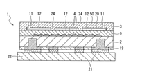
- the solid-state image pickup device of the tenth embodiment will be described with reference to the drawings.
- the basic configuration of the solid-state image pickup device of the tenth embodiment is the same as that of the ninth embodiment.
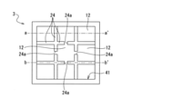
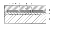
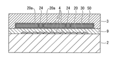
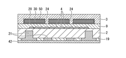
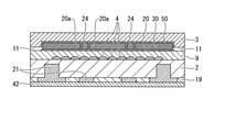
- the difference is that the support portion 24 is provided in the hollow portion 12. That is, the solid-state image sensor of the tenth form is the same as the solid-state image sensor of the ninth form except for the hollow portion 12.
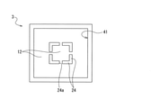
- ⁇ Hollow part 12> A recess is formed on the lower surface of the transparent substrate 3. The recess and the cavity surrounded by the flattening film 9 form the hollow portion 12.
- a columnar or wall-shaped support portion 24 projecting in the thickness direction of the transparent substrate 3 is integrally formed with the transparent substrate 3 in the recess. That is, the support portion 24 is made of the same material as the transparent substrate 3.
- a communication portion 3Aa is formed in a part of the support portion 24 to communicate the central chamber with the surrounding chambers.
- the lower end surfaces of the plurality of support portions 24 are flush with the lower end surfaces of the outer peripheral portion of the transparent substrate 3. Further, the arrangement of the support portion 24 is not particularly limited, and for example, the arrangement as shown in FIG. 13 may be used.
- the support portion 24 is a one or more columnar or wall-shaped structure that connects the lower surface of the transparent substrate 3 and the flattening film 9 in the hollow portion 12, the shape and number thereof are particularly high. , There is no particular limitation on the arrangement. In FIGS. 11 and 13, the wall-shaped support portions 24 are formed so as to be continuous, but a plurality of support portions 24 may be independent of each other. The support portion 24 may project from the lower surface of the transparent substrate 3 toward the flattening film 9.
- the support portion 24 is arranged so as to form a chamber in the central portion, but for example, the support portion 24 may be arranged so as to form a rectangular pillar in the central portion.
- the support portion 24 may be provided in another form.
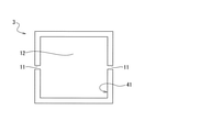
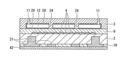
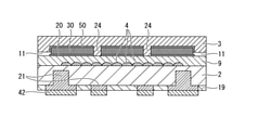
- a through hole 11 is formed in the transparent substrate 3. As shown in FIG. 12A, the through hole 11 is arranged at a position facing the outer peripheral region ARA2 of the substrate 2 on which the element is formed in a plan view. It extends in the thickness direction of the transparent substrate 3.
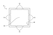
- the number and arrangement positions of the through holes 11 are set so as to communicate with any of the chambers even when the recess 41 is divided into a plurality of chambers by the support portion 24.
- the eight outer peripheral chambers are independent, eight through holes 11 are arranged so as to communicate with each chamber.
- Other configurations are the same as those of the ninth embodiment.
- the solid-state image pickup device of the eleventh embodiment will be described with reference to the drawings.
- the basic configuration of the eleventh form is the same as that of the tenth form, as shown in FIGS. 14, 15A and 15B.
- the eleventh form is the same as the tenth form except that the material of the support portion 24 is different.
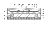
- the support portion 24 is arranged in the hollow portion 12.
- the support portion 24 is made of a resin material different from that of the transparent substrate 3.
- the support portion 24 is made of a light-transmitting resin material.
- the support portion 24 is made of, for example, the same resin material as the sacrificial layer described later.
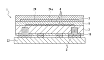
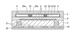
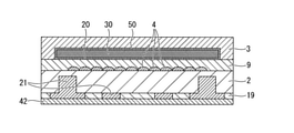
- a low refraction film 20a is formed on the surface of the support portion 24. Therefore, when the sacrificial layer is etched through the through hole 11 to remove the sacrificial layer, the sacrificial layer constituting the support portion 24 can remain in the hollow portion 12.
- the support portion 24 may be made of a resin material other than the sacrificial layer and which is not removed when the sacrificial layer is etched.
- the other configurations of the eleventh form are the same as those of the tenth form.
- the arrangement of the support portion 24 is not particularly limited, and may be the arrangement as shown in FIG. 16, for example.
- the solid-state image pickup device of the twelfth embodiment will be described with reference to the drawings.
- the basic configuration of the twelfth form is the same as that of the ninth form.
- the twelfth form has the same configuration as the ninth form except that the formation position of the through hole 11 is different.
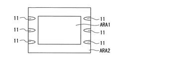
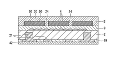
- the through hole 11 is formed so as to open in the side wall portion of the transparent substrate 3. That is, the through hole 11 extends from the side surface of the recess 41 formed in the transparent substrate 3 in a direction intersecting the plate thickness direction of the transparent substrate 3 (in this example, a direction orthogonal to each other).
- the through hole 11 may be formed at any position as long as it can face the outer peripheral region ARA2 of the substrate 2 on which the element is formed in a plan view.
- FIGS. 18A, 18B, and 18C Examples of the formation positions of the through holes 11 are shown in FIGS. 18A, 18B, and 18C.
- the through holes 11 are formed on the two side portions facing each other on the left and right sides of the transparent substrate 3.
- the through holes 11 are formed on the four sides of the transparent substrate 3, respectively.
- a plurality of through holes 11 are formed on each side.
- the through hole 11 is formed in a groove shape at the lower end of the transparent substrate, and the lower surface of the through hole 11 is formed of the flattening film 9, but the through hole 11 is illustrated. May have a shape that penetrates the side portion of the transparent substrate (see FIG. 29A and the like), or may extend laterally so as to penetrate the flattening film 9.
- the other configurations of the twelfth form are the same as those of the ninth form.
- the solid-state image pickup device of the thirteenth embodiment will be described with reference to the drawings.
- the basic configuration of the thirteenth form is the same as that of the tenth form, as shown in FIGS. 20A, 20B, and 19.
- the twelfth form has the same configuration as the tenth form except that the formation position of the through hole 11 and the support portion 24 are different.
- the through hole 11 is formed so as to open in the side wall portion of the transparent substrate 3. That is, the through hole 11 extends from the side surface of the recess 41 formed in the transparent substrate 3 in a direction intersecting the plate thickness direction of the transparent substrate 3 (in this example, a direction orthogonal to each other).
- the through hole 11 may be formed at any position as long as it can face the outer peripheral region ARA2 of the substrate 2 on which the element is formed in a plan view.
- ⁇ Support part 24> As shown in FIG. 19, the arrangement of the support portion 24 is the same as that of the tenth embodiment. However, since the through hole 11 is provided on the side wall, a communication passage 24a for communicating with the through hole 11 is formed in each support portion 24. Another example of the arrangement of the support portion 24 is shown in FIG. In this example, a columnar support portion 24 is provided in the central portion of the recess 41. The other configurations of the twelfth form are the same as those of the tenth form.
- the solid-state image sensor of the fourteenth embodiment will be described with reference to the drawings.
- the basic configuration of the fourteenth form is the same as that of the thirteenth form, as shown in FIGS. 22, 23A and 23B.
- the fourteenth form has the same configuration as the thirteenth form except that the material of the support portion 24 is different.
- the support portion 24 is made of a resin material different from that of the transparent substrate 3. However, it is made of a light-transmitting resin material.
- the support portion 24 is made of, for example, the same resin material as the sacrificial layer described later.
- a low refraction film 20a is formed on the surface of the support portion 24. Therefore, even if the sacrificial layer is removed by etching through the through hole 11, the sacrificial layer constituting the support portion 24 can remain.
- the other configurations of the fourteenth form are the same as those of the thirteenth form.
- the solid-state image pickup device of the fifteenth embodiment will be described with reference to the drawings.
- the basic configuration of the fifteenth form is the same as that of the thirteenth form.
- the fifteenth form has the same configuration as the thirteenth form except that the formation position of the through hole 11 is different.
- the through hole 11 is formed in both the glass side wall portion and the transparent substrate 3 in the thickness direction.
- the support portion 24 may be omitted. Further, the support portion 24 may be made of a material different from that of the transparent substrate 3.
- the other configurations of the fifteenth form are the same as those of the thirteenth form.
- the through hole 11 will be supplementarily described.
- the through hole 11 may not be formed so as to extend in the thickness direction as long as it is formed in the outer peripheral region ARA2 in a plan view. Further, the through hole 11 may be provided in the transparent substrate 3 or may be formed at a position where the adhesive layer 10 between the flattening film 9 formed on the substrate 2 on which the element is formed and the transparent substrate 3 is provided. good.
- the adhesive layer 10 provided on the flattening film 9 is preferably provided in the outer peripheral region ARA 2 excluding the effective pixel region ARA 1.
- the through hole 11 may have a slit in cross section or a hole shape such as a circle or a rectangle in cross section. That is, as long as the through hole 11 is formed in the outer peripheral region ARA2, the opening cross section of the through hole 11 is not limited.
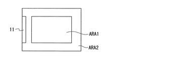
- FIG. 25A illustrates a case where the slit-shaped through hole 11 is opened in the plate thickness direction and is formed on one of the four sides of the outer peripheral region ARA2.
- FIG. 25B illustrates a case where the slit-shaped through hole 11 is opened in the plate thickness direction and is formed on three of the four sides of the outer peripheral region ARA2.
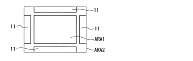
- FIG. 25C illustrates a case where the slit-shaped through hole 11 is opened in the plate thickness direction and is formed on four of the four sides of the outer peripheral region ARA2.
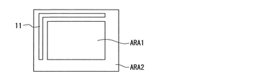
- FIG. 25D illustrates a case where the slit-shaped through hole 11 is opened in the plate thickness direction and is formed in an L shape across two adjacent sides of the outer peripheral region ARA2.
- FIG. 25E illustrates a case where the slit-shaped through holes 11 are opened in the plate thickness direction and two sets are formed in an L shape straddling two adjacent sides of the outer peripheral region ARA2.
- FIG. 25F illustrates a case where the slit-shaped through hole 11 is opened on the side surface and is formed on one of the four sides of the outer peripheral region ARA2.
- FIG. 25G illustrates a case where the slit-shaped through hole 11 is opened on the side surface and is formed on two of the four sides of the outer peripheral region ARA2.
- FIG. 25H illustrates a case where the slit-shaped through hole 11 is opened on the side surface and is formed on three of the four sides of the outer peripheral region ARA2.
- FIG. 25I illustrates a case where the slit-shaped through hole 11 is opened on the side surface and is formed on four of the four sides of the outer peripheral region ARA2.
- FIG. 25J illustrates a case where the slit-shaped through hole 11 is opened on the side surface and is formed in an L shape across two adjacent sides of the outer peripheral region ARA2.
- FIG. 25K illustrates a case where the slit-shaped through holes 11 are opened on the side surface and two sets are formed in an L shape straddling two adjacent sides of the outer peripheral region ARA2.
- FIG. 25L illustrates a case where the slit-shaped through hole 11 is opened on the side surface and formed on the entire circumference of the side surface.
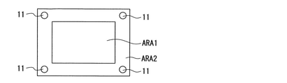
- FIG. 26A illustrates a case where the through hole 11 is opened in the plate thickness direction and is formed at the four corners of the outer peripheral region ARA2.
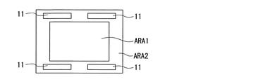
- FIG. 26B illustrates a case where the through hole 11 is opened in the plate thickness direction and is formed at the four corners and four sides of the outer peripheral region ARA2.
- FIG. 26C illustrates a case where the rectangular through hole 11 is opened in the plate thickness direction and the long side is directed to each of the corresponding two sides of the four sides of the outer peripheral region ARA2. .. FIG.
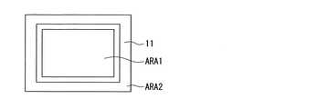
- FIG. 26D illustrates a case where the rectangular through hole 11 is opened in the plate thickness direction and is formed so as to surround the pixel region along the outer peripheral region ARA2.
- FIG. 26E illustrates a case where a plurality of through holes 11 are opened in the plate thickness direction and a plurality of through holes 11 are formed along one of the four sides of the outer peripheral region ARA2.
- FIG. 26F illustrates a case where a plurality of through holes 11 are opened in the plate thickness direction and a plurality of through holes 11 are formed on opposite two sides of the four sides of the outer peripheral region ARA2.
- FIG. 26G illustrates a case where a plurality of through holes 11 are opened in the plate thickness direction and a plurality of through holes 11 are formed along three of the four sides of the outer peripheral region ARA2.
- FIG. 26H illustrates a case where a plurality of through holes 11 are opened in the plate thickness direction and a plurality of through holes 11 are formed along four of the four sides of the outer peripheral region ARA2.
- FIG. 28A illustrates a case where a plurality of through holes 11 are opened on the side surface and a plurality of through holes 11 are formed along one of the four sides of the outer peripheral region ARA2.
- FIG. 28B illustrates a case where a plurality of through holes 11 are opened on the side surface and a plurality of through holes 11 are formed on opposite two sides of the four sides of the outer peripheral region ARA2.
- FIG. 28A illustrates a case where a plurality of through holes 11 are opened on the side surface and a plurality of through holes 11 are formed along one of the four sides of the outer peripheral region ARA2.
- FIG. 28B illustrates a case where a plurality of through holes 11 are opened on the side surface and a plurality of through holes 11 are formed on opposite two sides of the four sides of the outer peripheral
- FIG. 28C illustrates a case where a plurality of through holes 11 are opened on the side surface and a plurality of through holes 11 are formed along three of the four sides of the outer peripheral region ARA2.
- FIG. 28D illustrates a case where a plurality of through holes 11 are opened on the side surface and a plurality of through holes 11 are formed along four of the four sides of the outer peripheral region ARA2.
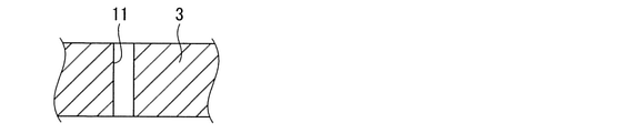
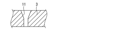
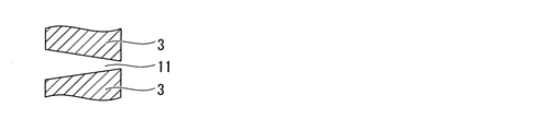
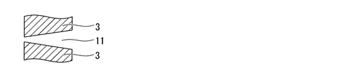
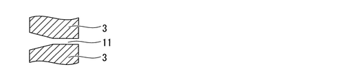
- FIGS. 27A to 27F can be exemplified as the cross-sectional shape of the through hole 11 extending in the plate thickness direction.
- FIG. 27A illustrates a case where the through hole 11 is formed in the thickness direction and the opening cross-sectional area is constant in the axial direction.
- FIG. 27B illustrates a case where the through hole 11 is formed diagonally with respect to the thickness direction and the opening cross-sectional area is constant in the axial direction.
- FIG. 27C illustrates a case where the through hole 11 is formed in the thickness direction and the opening cross-sectional area becomes smaller toward the lower side along the axial direction.
- FIG. 27A illustrates a case where the through hole 11 is formed in the thickness direction and the opening cross-sectional area is constant in the axial direction.
- FIG. 27D illustrates a case where the through hole 11 is formed in the thickness direction and the opening cross-sectional area becomes larger toward the lower side along the axial direction.
- FIG. 27E illustrates a case where the through hole 11 is formed in the thickness direction, and the opening cross-sectional area becomes larger toward the lower side along the axial direction only on the upper surface side.
- FIG. 27F illustrates a case where the through hole 11 is formed in the thickness direction and the opening cross-sectional area is expanded in a trapezoidal shape only on the upper surface side.
- FIGS. 29A to 29E can be exemplified as the cross-sectional shape of the through hole 11 when the through hole 11 is formed on the side wall.
- FIG. 29A illustrates a case where the through hole 11 is formed in a direction orthogonal to the thickness direction and the opening cross-sectional area is constant in the axial direction.
- FIG. 29B illustrates a case where the through hole 11 is formed at an angle from a direction orthogonal to the thickness direction and the opening cross-sectional area is constant in the axial direction.
- FIG. 29C illustrates a case where the through hole 11 is formed in a direction orthogonal to the thickness direction and the opening cross-sectional area becomes smaller toward the inside along the axial direction.
- FIG. 29A illustrates a case where the through hole 11 is formed in a direction orthogonal to the thickness direction and the opening cross-sectional area is constant in the axial direction.
- FIG. 29C illustrates a case where the through hole 11 is formed in a direction orthogonal to the thickness direction
- FIG. 29D illustrates a case where the through hole 11 is formed in a direction orthogonal to the thickness direction, and the opening cross-sectional area increases inward along the axial direction.
- FIG. 29E illustrates a case where the through hole 11 is formed in the thickness direction and the opening cross-sectional area is expanded only on the hollow portion 12 side.
- the seal member 13 will be supplementarily described.
- the structure of the seal member 13 is not limited as long as the through hole 11 can be closed. That is, the embedded shape of the seal member 13 may be such that the through hole 11 is embedded and closed, and the shape is not particularly limited.
- the upper surface of the seal member 13 may be the same as the upper surface of the transparent substrate 3, the upper surface of the seal member 13 may be convexly projected or recessed with respect to the upper surface of the transparent substrate 3.
- the seal member 13 may be provided so as to close only a part of the through hole 11 in the axial direction as shown in FIG. 30A, or may be provided so as to close the entire axial direction of the through hole 11 as shown in FIG. 30B. good. Further, the seal member 13 may have a portion protruding from the through hole 11 as shown in FIG. 30C, or may be recessed from the open end of the through hole 11.
- the size of the transparent substrate 3 is, for example, the size of a wafer.
- the transparent substrate 3 is made of, for example, a glass substrate.
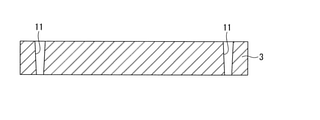
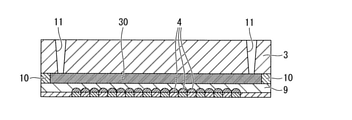
- the transparent substrate 3 shown in FIG. 31A is subjected to a process of forming a through hole 11 in the thickness direction as shown in FIG. 31B.
- the through hole 11 is formed at a position facing the outer peripheral region ARA 2 in the thickness direction of the transparent substrate 3.
- the shape and number of open cross sections of the through holes 11 are not particularly limited.
- the process of forming the through hole 11 is performed by, for example, dry etching, wet etching, laser processing, or the like.
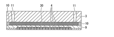
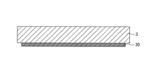
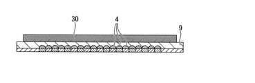
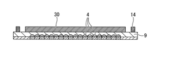
- a sacrificial layer is formed on the lower surface of the transparent substrate 3 on which the through hole 11 is formed.
- the sacrificial layer is formed in a position facing the entire effective pixel region ARA 1 and a region including the lower surface of the transparent substrate 3 in which the through hole 11 is formed.
- the sacrificial layer is formed so that the portion where the adhesive layer 10 is provided remains at the entire peripheral position on the outer peripheral side of the sacrificial layer forming position on the lower surface of the transparent substrate 3.
- a silicon substrate is attached to the lower surface of the transparent substrate 3 by using an anode bond or the like. After that, an unnecessary part of the attached silicon substrate is removed by etching to use it as a sacrificial layer.
- the unnecessary portion is a portion on the outer peripheral side of the position facing the bottom of the through hole 11 and where the adhesive layer 10 is provided.
- the material of the sacrificial layer include single crystal silicon, polycrystalline silicon, amorphous silicon, and silicon nitride film.
- the flattening film 9 may be formed before, after, or at the same time as the formation of the transparent substrate 3.
- the flattening film 9 is formed on the upper surface (eyes on the light incident surface side) of the substrate 2 on which the element is formed so as to completely cover the on-chip lens 4 shown in FIG. 32A.
- the substrate 2 on which the element in this state is formed is the substrate 2 on which the element of the solid-state image pickup element 1 (CCD, CMOS, surface irradiation type, etc.) is formed.
- the on-chip lens 4 microwaves
- the on-chip lens 4 is formed on the light incident surface side of the substrate 2 on which the element is formed, and the wiring on the back surface side is formed. It is assumed that it has not been performed.
- an ultraviolet curable type, a thermosetting type, or a resin having a curing reaction mechanism combined with them is used as the material of the flattening film 9.
- resins include acrylic, styrene, and silicone resins.
- Fluorine may be appropriately contained in such a resin, or hollow silica or the like may be dispersed and mixed.
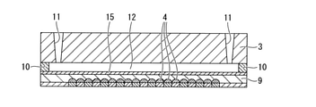
- the formed transparent substrate 3 is attached and laminated on the flattening film 9.
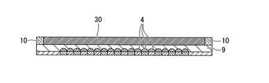
- an adhesive layer 10 is formed on the outer peripheral portion of the sacrificial layer, and the transparent substrate 3 on the flattening film 9 is attached by the adhesive layer 10.
- the adhesive layer 10 may be formed on the upper side of the flattening film 9 and the sticking process may be executed, or may be formed on the transparent substrate 3 side and the sticking process may be executed. As a result, the adhesive layer 10 is arranged on the entire circumference in the outer peripheral direction of the sacrificial layer.
- an ultraviolet curable type, a thermosetting type, or a sealing resin having a curing reaction mechanism thereof may be used as the material of the adhesive layer 10.
- the sealing resin include epoxy-based, acrylic-based, and silicone-based sealing resins, and modified resins thereof.
- rewiring processing (wiring processing on the back surface side) such as RDL, solder balls 6, and lead wiring is executed on the back surface side of the substrate 2 on which the element is formed. In this state, there is a sacrificial layer.
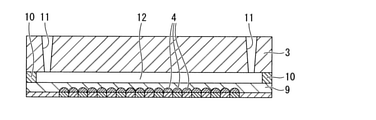
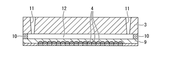
- ⁇ Formation process of hollow portion 12> When the rewiring process is completed, as shown in FIG. 32C, the sacrificial layer is etched through the through hole 11 to remove the sacrificial layer. As a result, a cavity is formed at the position where the sacrificial layer was present. The hollow portion becomes the hollow portion 12.
- the hollow portion 12 is composed of a cavity surrounded by the upper surface of the flattening film 9, the lower surface of the transparent substrate 3, and the inner peripheral surface of the adhesive layer 10.
- Etching of the sacrificial layer is performed by using, for example, a dry etching method. At this time, examples of the gas type used for dry etching include XeF 2 , ClF 3 , and BrF 3 .
- etching with a high selectivity of 1000 or more is possible with SiO 2 , resin, Al, TiN, SiC and the like.
- the side wall of the hollow portion 12 is formed by the adhesive layer 10, but by using a resin for the adhesive layer 10, the etching removability of the sacrificial layer becomes good.
- the seal member 13 may be formed without being formed. When forming the seal member 13, as shown in FIG. 32D, the seal member 13 closes and seals the through hole 11.
- the seal member 13 uses, for example, an ultraviolet curable type, a thermosetting type, or a resin having a curing reaction mechanism combined with them.
- resins include epoxy-based, acrylic-based, and silicone-based resins, or modified resins of these resins.
- the second manufacturing method will be described with reference to the drawings.
- ⁇ Formation of transparent substrate 3> A second example of the method for forming the transparent substrate 3 will be described.
- the sacrificial layer is formed and then the through hole 11 is formed. That is, in the second example, first, a sacrificial layer is formed on the lower surface of the transparent substrate 3 before the formation of the through hole 11 as shown in FIG. 33A.
- the sacrificial layer is formed in a position facing the entire effective pixel region ARA 1 and a region including the lower surface of the transparent substrate 3 forming the through hole 11.
- the formation of the sacrificial layer is performed so that a portion on the lower surface of the transparent substrate 3 where the adhesive layer 10 is provided remains at the entire peripheral position on the outer peripheral side of the sacrificial layer.
- a film of polycrystalline silicon, amorphous silicon, silicon nitriding, or the like is formed on the lower surface of the transparent substrate 3 by a CVD method or the like.
- a silicon substrate is attached to the lower surface of the transparent substrate 3 by using an anode bond or the like.
- an unnecessary part of the formed sacrificial layer is removed by etching to obtain a sacrificial layer.
- the unnecessary portion is a portion on the outer peripheral side of the position where the bottom of the through hole 11 is provided and where the adhesive layer 10 is provided.
- the material of the silicon substrate include single crystal silicon, polycrystalline silicon, amorphous silicon, and a silicon nitride film.
- the transparent substrate 3 on which the sacrificial layer is formed is subjected to a process of forming a through hole 11 from above in the thickness direction.
- the through hole 11 is formed at a position facing the outer peripheral region ARA 2 in the thickness direction of the transparent substrate 3.
- the through hole 11 is opened so as to penetrate the sacrificial layer together.
- the shape and number of open cross sections of the through holes 11 are not particularly limited.
- the process of forming the through hole 11 is performed by, for example, dry etching, wet etching, laser processing, or the like.
- a flattening film 9 is formed on the upper surface of the substrate 2 on which the element is formed.
- the flattening film 9 may be formed before, after, or at the same time as the formation of the transparent substrate 3.
- the formed transparent substrate 3 is attached and laminated on the flattening film 9.
- an adhesive layer 10 is formed on the outer peripheral portion of the sacrificial layer, and the transparent substrate 3 on the flattening film 9 is attached by the adhesive layer 10.
- the adhesive layer 10 may be formed on the upper side of the flattening film 9 and the sticking process may be executed, or may be formed on the transparent substrate 3 side and the sticking process may be executed. As a result, the adhesive layer 10 is arranged on the entire circumference in the outer peripheral direction of the sacrificial layer.
- an ultraviolet curable type, a thermosetting type, or a sealing resin having a curing reaction mechanism thereof may be used as the material of the adhesive layer 10.
- the sealing resin include epoxy-based, acrylic-based, and silicone-based sealing resins, and modified resins thereof.
- the hollow portion 12 is composed of a cavity surrounded by the upper surface of the flattening film 9, the lower surface of the transparent substrate 3, and the inner peripheral surface of the adhesive layer 10.
- Etching of the sacrificial layer is performed by using, for example, a dry etching method.
- the gas type used for dry etching include XeF 2 , ClF 3 , and BrF 3 .
- the seal member 13 may be formed without being formed.
- the seal member 13 closes and seals the through hole 11.
- the solid-state imaging device 1 of the first embodiment can be manufactured.
- the third manufacturing method will be described with reference to the drawings.
- ⁇ Formation of transparent substrate 3> A third example of the method for forming the transparent substrate 3 will be described.
- the sacrificial layer is formed and then the through hole 11 is formed. Further, in the third example, the spacer 14 is formed at the lower end portion of the transparent substrate 3.
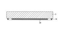
- a sacrificial layer is formed on the lower surface of the transparent substrate 3 before the formation of the through hole 11 as shown in FIG. 35A.
- the sacrificial layer is formed in a region including a position facing the entire effective pixel region ARA 1, a lower surface of the transparent substrate 3 forming the through hole 11, and a part of a portion forming the adhesive layer 10.
- the portion 14 of the sacrificial layer formed in the outer peripheral region ARA 2 where the adhesive layer 10 is provided has a portion (a portion serving as a spacer 14) where the adhesive layer 10 is provided remaining on the inner peripheral side and the outer peripheral side thereof.
- the portion of the sacrificial layer on the outer peripheral side may be formed on the entire circumference in the circumferential direction along the outer peripheral region ARA2, may be formed on the side portions on both the left and right sides, or may be formed intermittently along the circumferential direction. It may be formed in.
- a silicon substrate is attached to the lower surface of the transparent substrate 3 by using an anode bond or the like. After that, an unnecessary part of the formed sacrificial layer is removed by etching to obtain a sacrificial layer.
- the unnecessary portion is a portion on the outer peripheral side of the position where the bottom of the through hole 11 is provided and where the adhesive layer 10 is provided.
- the material of the silicon substrate include single crystal silicon, polycrystalline silicon, amorphous silicon, and a silicon nitride film.
- the transparent substrate 3 on which the sacrificial layer is formed is subjected to a process of forming a through hole 11 in the thickness direction as shown in FIG. 35B.
- the through hole 11 is formed at a position facing the outer peripheral region ARA 2 in the thickness direction of the transparent substrate 3.
- the through hole 11 is opened so as to penetrate the sacrificial layer together.
- the shape and number of open cross sections of the through holes 11 are not particularly limited.
- the process of forming the through hole 11 is performed by, for example, dry etching, wet etching, laser processing, or the like.
- the portion between the formed through hole 11 and the portion 14 of the sacrificial layer located on the outer peripheral side thereof is exposed.
- the flattening film 9 may be formed before, after, or at the same time as the formation of the transparent substrate 3.
- the flattening film 9 is formed so as to completely cover the on-chip lens 4 with respect to the upper surface (eyes on the light incident surface side) of the substrate 2 on which the element is formed.
- the formed transparent substrate 3 is attached and laminated on the flattening film 9.
- an adhesive layer 10 is formed on the outer peripheral portion of the sacrificial layer, and the transparent substrate 3 on the flattening film 9 is attached by the adhesive layer 10.
- the adhesive layer 10 may be formed on the upper side of the flattening film 9 and the sticking process may be executed, or may be formed on the transparent substrate 3 side and the sticking process may be executed. As a result, the adhesive layer 10 is arranged on the entire circumference in the outer peripheral direction of the sacrificial layer.
- an ultraviolet curable type, a thermosetting type, or a sealing resin having a curing reaction mechanism thereof may be used as the material of the adhesive layer 10.
- the sealing resin include epoxy-based, acrylic-based, and silicone-based sealing resins, and modified resins thereof.
- the portion 14 of the sacrificial layer located on the outer peripheral side is embedded in the adhesive layer 10 to form the spacer 14.
- the adhesive layer 10 is present on the inner peripheral side of the sacrificial layer portion 14 located on the outer peripheral side thereof and at the outer peripheral side position from the bottom position of the through hole 11.
- ⁇ Formation process of hollow portion 12> When the rewiring process is completed, as shown in FIG. 36B, the sacrificial layer is etched through the through hole 11 to remove the sacrificial layer. As a result, a cavity is formed at the position where the sacrificial layer was present. The hollow portion becomes the hollow portion 12.
- the hollow portion 12 is composed of a cavity surrounded by the upper surface of the flattening film 9, the lower surface of the transparent substrate 3, and the inner peripheral surface of the adhesive layer 10.
- Etching of the sacrificial layer is performed by using, for example, a dry etching method. At this time, examples of the gas type used for dry etching include XeF 2 , ClF 3 , and BrF 3 .
- the portion of the sacrificial layer embedded in the adhesive layer 10 on the outer peripheral side remains unetched by the sealing resin of the adhesive layer 10 located on the inner peripheral side thereof, and becomes a spacer 14.
- the seal member 13 may be formed without being formed. When forming the seal member 13, as shown in FIG. 36C, the seal member 13 closes and seals the through hole 11.
- the solid-state image sensor 1 in the second form can be manufactured by the third manufacturing method.
- the fourth manufacturing method will be described with reference to the drawings.
- ⁇ Formation of transparent substrate 3> A fourth example of the method for forming the transparent substrate 3 will be described.
- the sacrificial layer is formed and then the through hole 11 is formed. Further, in the fourth example, the spacer 14 is formed at the lower end portion of the transparent substrate 3.
- a sacrificial layer is formed on the lower surface of the transparent substrate 3 before the formation of the through hole 11 as shown in FIG. 37A.
- the sacrificial layer is formed in a region including a position facing the entire effective pixel region ARA 1, a lower surface of the transparent substrate 3 forming the through hole 11, and a part of a portion forming the adhesive layer 10.
- the portion of the sacrificial layer (the portion that becomes the spacer 14) formed in the outer peripheral region ARA 2 where the adhesive layer 10 is provided leaves a portion where the adhesive layer 10 is provided on the inner peripheral side and the outer peripheral side thereof. Form like this.
- the portion of the sacrificial layer on the outer peripheral side may be formed on the entire circumference in the circumferential direction along the outer peripheral region ARA2, may be formed on the side portions on both the left and right sides, or may be formed intermittently along the circumferential direction. It may be formed in.
- the sacrificial layer for example, first, polycrystalline silicon, amorphous silicon, silicon nitriding, or the like is formed on the lower surface of the transparent substrate 3 by a CVD method or the like. After that, an unnecessary part of the formed sacrificial layer is removed by etching to obtain a sacrificial layer.
- the unnecessary portion is a portion on the outer peripheral side of the position where the bottom of the through hole 11 is provided and where the adhesive layer 10 is provided.
- the transparent substrate 3 on which the sacrificial layer is formed is subjected to a process of forming a through hole 11 in the thickness direction as shown in FIG. 37.
- the through hole 11 is formed at a position facing the outer peripheral region ARA 2 in the thickness direction of the transparent substrate 3.
- the through hole 11 is opened so as to penetrate the sacrificial layer together.
- the shape and number of open cross sections of the through holes 11 are not particularly limited.
- the process of forming the through hole 11 is performed by, for example, dry etching, wet etching, laser processing, or the like.
- the portion between the formed through hole 11 and the sacrificial layer on the outer peripheral side is exposed.
- the flattening film 9 may be formed before, after, or at the same time as the formation of the transparent substrate 3.
- the flattening film 9 is formed so as to completely cover the on-chip lens 4 with respect to the upper surface (eyes on the light incident surface side) of the substrate 2 on which the element is formed.
- the formed transparent substrate 3 is attached and laminated on the flattening film 9.
- an adhesive layer 10 is formed on the outer peripheral portion of the sacrificial layer, and the transparent substrate 3 on the flattening film 9 is attached by the adhesive layer 10.
- the adhesive layer 10 may be formed on the upper side of the flattening film 9 and the sticking process may be executed, or may be formed on the transparent substrate 3 side and the sticking process may be executed. As a result, the adhesive layer 10 is arranged on the entire circumference in the outer peripheral direction of the sacrificial layer.
- an ultraviolet curable type, a thermosetting type, or a sealing resin having a curing reaction mechanism thereof may be used as the material of the adhesive layer 10.
- the sealing resin include epoxy-based, acrylic-based, and silicone-based sealing resins, and modified resins thereof.
- the portion of the sacrificial layer located on the outer peripheral side is embedded in the adhesive layer 10 to form the spacer 14.
- the adhesive layer 10 is present on the inner peripheral side of the sacrificial layer portion located on the outer peripheral side thereof and at the outer peripheral side position from the position of the bottom of the through hole 11.
- ⁇ Formation process of hollow portion 12> When the rewiring process is completed, as shown in FIG. 38B, the sacrificial layer is etched through the through hole 11 to remove the sacrificial layer. As a result, a cavity is formed at the position where the sacrificial layer was present. The hollow portion becomes the hollow portion 12.
- the hollow portion 12 is composed of a cavity surrounded by the upper surface of the flattening film 9, the lower surface of the transparent substrate 3, and the inner peripheral surface of the adhesive layer 10.
- Etching of the sacrificial layer is performed by using, for example, a dry etching method. At this time, examples of the gas type used for dry etching include XeF 2 , ClF 3 , and BrF 3 .
- the portion of the sacrificial layer embedded in the adhesive layer 10 on the outer peripheral side remains unetched by the sealing resin of the adhesive layer 10 located on the inner peripheral side thereof, and becomes a spacer 14.
- the seal member 13 may be formed without being formed.
- the seal member 13 closes and seals the through hole 11.
- the solid-state imaging device 1 of the second embodiment can be manufactured.
- the fifth manufacturing method will be described with reference to the drawings.
- ⁇ Formation of transparent substrate 3> A fifth example of the method for forming the transparent substrate 3 will be described.
- the through hole 11 is formed in the transparent substrate 3, but the sacrificial layer is not formed. That is, in the fifth example, as shown in FIG. 39, the process of forming the through hole 11 in the thickness direction is performed. As described above, the through hole 11 is formed at a position facing the outer peripheral region ARA 2 in the thickness direction of the transparent substrate 3.
- the shape and number of open cross sections of the through holes 11 are not particularly limited.
- the process of forming the through hole 11 is performed by, for example, dry etching, wet etching, laser processing, or the like.
- the flattening film 9 may be formed before, after, or at the same time as the formation of the transparent substrate 3. As shown in FIG. 40A, the flattening film 9 is formed so as to completely cover the on-chip lens 4 on the upper surface (eyes on the light incident surface side) of the substrate 2 on which the element is formed.
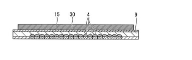
- a sacrificial layer is formed on the flattening film 9 as shown in FIG. 40A.
- the sacrificial layer is formed in the entire effective pixel region ARA 1 and a region including a position facing the bottom of the through hole 11.
- the formation of the sacrificial layer is performed so that a portion where the adhesive layer 10 is provided remains at the entire peripheral position on the outer peripheral side of the sacrificial layer.
- a film of polycrystalline silicon, amorphous silicon, silicon nitriding, or the like is formed on the lower surface of the transparent substrate 3 by a CVD method or the like.
- a silicon substrate is attached to the lower surface of the transparent substrate 3 by using an anode bond or the like.
- an unnecessary part of the formed sacrificial layer is removed by etching to obtain a sacrificial layer.
- the unnecessary portion is a portion on the outer peripheral side of the position facing the bottom of the through hole 11 and where the adhesive layer 10 is provided.
- the material of the silicon substrate include single crystal silicon, polycrystalline silicon, amorphous silicon, and a silicon nitride film.
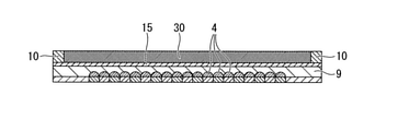
- the adhesive layer 10 is formed on the entire outer circumference of the sacrificial layer on the upper surface of the flattening film 9.
- the adhesive layer 10 is formed higher than the sacrificial layer to earn a crushing allowance.
- an ultraviolet curable type, a thermosetting type, or a sealing resin having a curing reaction mechanism thereof may be used as the material of the adhesive layer 10.
- the sealing resin include epoxy-based, acrylic-based, and silicone-based sealing resins, and modified resins thereof.
- ⁇ Formation process of hollow portion 12> When the rewiring process is completed, as shown in FIG. 40D, the sacrificial layer is etched through the through hole 11 to remove the sacrificial layer. As a result, a cavity is formed at the position where the sacrificial layer was present. The hollow portion becomes the hollow portion 12.
- the hollow portion 12 is composed of a cavity surrounded by the upper surface of the flattening film 9, the lower surface of the transparent substrate 3, and the inner peripheral surface of the adhesive layer 10.
- Etching of the sacrificial layer is performed by using, for example, a dry etching method. At this time, examples of the gas type used for dry etching include XeF 2 , ClF 3 , and BrF 3 .
- the portion of the sacrificial layer embedded in the adhesive layer 10 on the outer peripheral side remains unetched by the sealing resin of the adhesive layer 10 located on the inner peripheral side thereof, and becomes a spacer 14.
- the seal member 13 may be formed without being formed.
- the seal member 13 closes and seals the through hole 11.
- the solid-state imaging device 1 of the third embodiment can be manufactured.
- the flattening film 9 may be formed before, after, or at the same time as the formation of the transparent substrate 3.
- the flattening film 9 is formed so as to completely cover the on-chip lens 4 with respect to the upper surface (eyes on the light incident surface side) of the substrate 2 on which the element is formed.
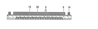
- a sacrificial layer is formed on the flattening film 9 as shown in FIG. 41A.
- the sacrificial layer is formed in a region including the entire effective pixel region ARA 1, a position facing the bottom of the through hole 11, and a part of a portion forming the adhesive layer 10.
- the portion 14 of the sacrificial layer formed in the outer peripheral region ARA 2 where the adhesive layer 10 is provided is formed so that the portion where the adhesive layer 10 is provided remains on the inner peripheral side and the outer peripheral side thereof.
- the portion of the sacrificial layer on the outer peripheral side may be formed on the entire circumference in the circumferential direction along the outer peripheral region ARA2, may be formed on the side portions on both the left and right sides, or may be formed intermittently along the circumferential direction. It may be formed in.
- a film of polycrystalline silicon, amorphous silicon, silicon nitriding, or the like is formed on the lower surface of the transparent substrate 3 by a CVD method or the like.
- a silicon substrate is attached to the lower surface of the transparent substrate 3 by using an anode bond or the like.
- an unnecessary part of the formed sacrificial layer is removed by etching to obtain a sacrificial layer.
- the unnecessary portion is a portion on the outer peripheral side of the position facing the bottom of the through hole 11 and where the adhesive layer 10 is provided.
- the material of the silicon substrate include single crystal silicon, polycrystalline silicon, amorphous silicon, and a silicon nitride film.
- the adhesive layer 10 is formed on the entire outer circumference of the sacrificial layer on the upper surface of the flattening film 9.
- the portion of the sacrificial layer located on the outer peripheral side is embedded in the adhesive layer 10 to form the spacer 14.
- the adhesive layer 10A is present on the inner peripheral side of the sacrificial layer portion located on the outer peripheral side thereof, and on the outer peripheral side position from the position facing the bottom position of the through hole 11. Further, the adhesive layer 10B is also present on the outer peripheral side of the sacrificial layer portion.
- an ultraviolet curable type, a thermosetting type, or a sealing resin having a curing reaction mechanism thereof may be used as the material of the adhesive layer 10.
- the sealing resin include epoxy-based, acrylic-based, and silicone-based sealing resins, and modified resins thereof.
- ⁇ Formation process of hollow portion 12> When the rewiring process is completed, as shown in FIG. 41D, the sacrificial layer is etched through the through hole 11 to remove the sacrificial layer. As a result, a cavity is formed at the position where the sacrificial layer was present. The hollow portion becomes the hollow portion 12.
- the hollow portion 12 is composed of a cavity surrounded by the upper surface of the flattening film 9, the lower surface of the transparent substrate 3, and the inner peripheral surface of the adhesive layer 10.
- Etching of the sacrificial layer is performed by using, for example, a dry etching method. At this time, examples of the gas type used for dry etching include XeF 2 , ClF 3 , and BrF 3 .
- the portion of the sacrificial layer embedded in the adhesive layer 10 on the outer peripheral side remains unetched by the sealing resin of the adhesive layer 10 located on the inner peripheral side thereof, and becomes a spacer 14.
- the seal member 13 may be formed without being formed.
- the seal member 13 closes and seals the through hole 11.
- the solid-state imaging device 1 of the fourth embodiment can be manufactured.
- the seventh manufacturing method will be described with reference to the drawings. ⁇ Formation of transparent substrate 3> Since the method of forming the transparent substrate 3 is the same as that of the fifth example, the description thereof will be omitted (see FIG. 39).
- the flattening film 9 may be formed before, after, or at the same time as the formation of the transparent substrate 3. As shown in FIG. 42A, the flattening film 9 is formed so as to completely cover the on-chip lens 4 on the upper surface (eyes on the light incident surface side) of the substrate 2 on which the element is formed.
- a layer 15 of the adhesive is formed on the flattening film 9.
- the adhesive layer 15 is preferably made of a resin material having a refractive index lower than that of the flattening film 9.
- the adhesive layer 15 is formed using a resinous adhesive.
- a resinous adhesive for example, an ultraviolet curable type, a thermosetting type, or a seal resin having a curing reaction mechanism thereof may be used.
- the sealing resin include epoxy-based, acrylic-based, and silicone-based sealing resins, and modified resins thereof.
- a sacrificial layer is formed on the adhesive layer 15 as shown in FIG. 42B.
- the sacrificial layer is formed in the entire effective pixel region ARA 1 and a region including a position facing the bottom of the through hole 11.
- the formation of the sacrificial layer is performed so that a portion where the adhesive layer 10 is provided remains at the entire peripheral position on the outer peripheral side of the sacrificial layer.
- the sacrificial layer for example, first, polycrystalline silicon, amorphous silicon, silicon nitriding, or the like is formed on the lower surface of the transparent substrate 3 by a CVD method or the like. Alternatively, a silicon substrate is attached to the lower surface of the transparent substrate 3 by using an anode bond or the like. After that, an unnecessary part of the formed sacrificial layer is removed by etching to obtain a sacrificial layer. The unnecessary portion is a portion on the outer peripheral side of the position facing the bottom of the through hole 11 and where the adhesive layer 10 is provided.
- Examples of the material of the silicon substrate include single crystal silicon, polycrystalline silicon, amorphous silicon, and a silicon nitride film.
- the adhesive layer 10 is formed on the entire outer circumference of the sacrificial layer on the upper surface of the adhesive layer 15.
- an ultraviolet curable type, a thermosetting type, or a sealing resin having a curing reaction mechanism thereof may be used as the material of the adhesive layer 10.
- the sealing resin include epoxy-based, acrylic-based, and silicone-based sealing resins, and modified resins thereof.
- the hollow portion 12 is composed of a cavity surrounded by the upper surface of the flattening film 9, the lower surface of the transparent substrate 3, and the inner peripheral surface of the adhesive layer 10.
- Etching of the sacrificial layer is performed by using, for example, a dry etching method.
- the gas type used for dry etching include XeF 2 , ClF 3 , and BrF 3 .
- the portion of the sacrificial layer embedded in the adhesive layer 10 on the outer peripheral side remains unetched by the sealing resin of the adhesive layer 10 located on the inner peripheral side thereof, and becomes a spacer 14.
- the seal member 13 may be formed without being formed.
- the seal member 13 closes and seals the through hole 11.
- the seventh manufacturing method for example, the solid-state imaging device 1 of the third embodiment can be manufactured.
- the flattening film 9 may be formed before, after, or at the same time as the formation of the transparent substrate 3. As shown in FIG. 43A, the flattening film 9 is formed so as to completely cover the on-chip lens 4 on the upper surface (eyes on the light incident surface side) of the substrate 2 on which the element is formed.
- a layer 15 of the adhesive is formed on the flattening film 9.
- the adhesive layer 15 is preferably made of a resin material having a refractive index lower than that of the flattening film 9.
- the adhesive layer 15 is formed using a resinous adhesive.
- a resinous adhesive for example, an ultraviolet curable type, a thermosetting type, or a seal resin having a curing reaction mechanism combined with them may be used.
- the sealing resin include epoxy-based, acrylic-based, and silicone-based sealing resins, and modified resins thereof.
- a sacrificial layer is formed on the adhesive layer 15 as shown in FIG. 42A.
- the sacrificial layer is formed in a region including the entire effective pixel region ARA 1, a position facing the bottom of the through hole 11, and a part of a portion forming the adhesive layer 10.
- the portion of the sacrificial layer formed in the outer peripheral region ARA2 where the adhesive layer 10 is provided is formed so that the portion where the adhesive layer 10 is provided remains on the inner peripheral side and the outer peripheral side thereof.
- the portion of the sacrificial layer on the outer peripheral side may be formed on the entire circumference in the circumferential direction along the outer peripheral region ARA2, may be formed on the side portions on both the left and right sides, or may be formed intermittently along the circumferential direction. It may be formed in.
- a film of polycrystalline silicon, amorphous silicon, silicon nitriding, or the like is formed on the lower surface of the transparent substrate 3 by a CVD method or the like.
- a silicon substrate is attached to the lower surface of the transparent substrate 3 by using an anode bond or the like.
- an unnecessary part of the formed sacrificial layer is removed by etching to obtain a sacrificial layer.
- the unnecessary portion is a portion on the outer peripheral side of the position facing the bottom of the through hole 11 and where the adhesive layer 10 is provided.
- the material of the silicon substrate include single crystal silicon, polycrystalline silicon, amorphous silicon, and a silicon nitride film.
- the adhesive layer 10 is formed on the entire outer circumference of the sacrificial layer on the upper surface of the flattening film 9.
- the portion of the sacrificial layer located on the outer peripheral side is embedded in the adhesive layer 10 to form the spacer 14.
- the adhesive layer 10A is present on the inner peripheral side of the sacrificial layer portion located on the outer peripheral side thereof, and on the outer peripheral side position from the position facing the bottom position of the through hole 11. Further, the adhesive layer 10B is also present on the outer peripheral side of the sacrificial layer portion.
- an ultraviolet curable type, a thermosetting type, or a sealing resin having a curing reaction mechanism thereof may be used as the material of the adhesive layer 10.
- the sealing resin include epoxy-based, acrylic-based, and silicone-based sealing resins, and modified resins thereof.
- the hollow portion 12 is composed of a cavity surrounded by the upper surface of the flattening film 9, the lower surface of the transparent substrate 3, and the inner peripheral surface of the adhesive layer 10.
- Etching of the sacrificial layer is performed by using, for example, a dry etching method.
- the gas type used for dry etching include XeF 2 , ClF 3 , and BrF 3 .
- the portion of the sacrificial layer embedded in the adhesive layer 10 on the outer peripheral side remains unetched by the sealing resin of the adhesive layer 10 located on the inner peripheral side thereof, and becomes a spacer 14.
- the seal member 13 may be formed without being formed.
- the seal member 13 closes and seals the through hole 11.
- the eighth manufacturing method for example, the solid-state image sensor 1 of the fourth embodiment can be manufactured.
- the ninth manufacturing method will be described with reference to the drawings.
- ⁇ Formation of transparent substrate 3> A sixth example of the method for forming the transparent substrate 3 will be described.
- the transparent substrate 3 of this example is configured by laminating a plurality of glass substrates.
- FIG. 44C a case where two glass substrates, an upper glass substrate 3A and a lower glass substrate 3B, are laminated will be described.
- a process of forming a through hole 11 in the thickness direction is performed on the upper glass substrate 3A as shown in FIG. 44A.
- the through hole 11 is formed at a position facing the outer peripheral region ARA 2 in the thickness direction of the transparent substrate 3.
- the shape and number of open cross sections of the through holes 11 are not particularly limited.
- the process of forming the through hole 11 is performed by, for example, dry etching, wet etching, laser processing, or the like.
- a sacrificial layer is formed on the lower surface of the transparent substrate 3 on which the through hole 11 is formed.
- the sacrificial layer is formed in a position facing the entire effective pixel region ARA 1 and a region including the lower surface of the transparent substrate 3 in which the through hole 11 is formed.
- the formation of the sacrificial layer is performed so that a portion on the lower surface of the transparent substrate 3 where the adhesive layer 10 is provided remains at the entire peripheral position on the outer peripheral side of the sacrificial layer.
- a silicon substrate is attached to the lower surface of the transparent substrate 3 by using an anode bond or the like. After that, an unnecessary part of the attached silicon substrate is removed by etching to use it as a sacrificial layer.
- the unnecessary portion is a portion on the outer peripheral side of the position facing the bottom of the through hole 11 and where the adhesive layer 10 is provided.
- the material of the sacrificial layer include single crystal silicon, polycrystalline silicon, amorphous silicon, and silicon nitride film.
- the adhesive layer 10 is formed on the entire outer circumference of the sacrificial layer on the lower surface of the upper glass substrate 3A.
- the material of the adhesive layer 10 for example, an ultraviolet curable type, a thermosetting type, or a sealing resin having a curing reaction mechanism thereof may be used.
- the sealing resin include epoxy-based, acrylic-based, and silicone-based sealing resins, and modified resins thereof.
- the lower glass substrate 3B is attached to the lower surface of the upper glass substrate 3A by the adhesive layer 10.
- the transparent substrate 3 of the sixth example is formed.
- the flattening film 9 may be formed before, after, or at the same time as the formation of the transparent substrate 3. As shown in FIG. 45A, the flattening film 9 is formed so as to completely cover the on-chip lens 4 on the upper surface (eyes on the light incident surface side) of the substrate 2 on which the element is formed.
- a layer 15 of the adhesive is formed on the flattening film 9.
- the adhesive layer 15 is preferably made of a resin material having a refractive index lower than that of the flattening film 9.
- the adhesive layer 10 is formed on the flattening film 9.
- the material of the adhesive layer 10 for example, an ultraviolet curable type, a thermosetting type, or a sealing resin having a curing reaction mechanism thereof may be used.
- the sealing resin include epoxy-based, acrylic-based, and silicone-based sealing resins, and modified resins thereof.
- the adhesive layer 10 is formed only in the outer peripheral region ARA2 on the flattening film 9.
- the hollow portion 12 is composed of a cavity surrounded by the upper surface of the flattening film 9, the lower surface of the transparent substrate 3, and the inner peripheral surface of the adhesive layer 10.
- Etching of the sacrificial layer is performed by using, for example, a dry etching method.
- the gas type used for dry etching include XeF 2 , ClF 3 , and BrF 3 .
- the portion of the sacrificial layer embedded in the adhesive layer 10 on the outer peripheral side remains unetched by the sealing resin of the adhesive layer 10 located on the inner peripheral side thereof, and becomes a spacer 14.
- the seal member 13 may be formed without being formed.
- the seal member 13 closes and seals the through hole 11.
- the ninth manufacturing method for example, the solid-state image sensor 1 of the fifth embodiment can be manufactured.
- the transparent substrate 3 of this example is configured by laminating a plurality of glass substrates.
- the spacer 14 is provided.
- a sacrificial layer is formed on the lower surface of the upper glass substrate 3A before the formation of the through hole 11 as shown in FIG. 46A.
- the sacrificial layer is formed in a region including a position facing the entire effective pixel region ARA 1, a lower surface of the transparent substrate 3 forming the through hole 11, and a part of a portion forming the adhesive layer 10.
- the portion 14 of the sacrificial layer formed in the outer peripheral region ARA 2 where the adhesive layer 10 is provided is formed so that the portion where the adhesive layer 10 is provided remains on the inner peripheral side and the outer peripheral side thereof.
- the portion of the sacrificial layer on the outer peripheral side may be formed on the entire circumference in the circumferential direction along the outer peripheral region ARA2, may be formed on the side portions on both the left and right sides, or may be formed intermittently along the circumferential direction. It may be formed in.
- the sacrificial layer for example, first, polycrystalline silicon, amorphous silicon, silicon nitriding, or the like is formed on the lower surface of the upper glass substrate 3A by a CVD method or the like. Alternatively, a silicon substrate is attached to the lower surface of the upper glass substrate 3A by using an anode bond or the like. After that, an unnecessary part of the formed sacrificial layer is removed by etching to obtain a sacrificial layer. The unnecessary portion is a portion on the outer peripheral side of the position facing the bottom of the through hole 11 and where the adhesive layer 10 is provided. Examples of the material of the silicon substrate include single crystal silicon, polycrystalline silicon, amorphous silicon, and a silicon nitride film.
- a process of forming a through hole 11 in the thickness direction is performed on the upper glass substrate 3A on which the sacrificial layer is formed.
- the through hole 11 is formed at a position facing the outer peripheral region ARA 2 in the thickness direction of the transparent substrate 3.
- the through hole 11 is opened so as to penetrate the sacrificial layer together.
- the shape and number of open cross sections of the through holes 11 are not particularly limited.
- the process of forming the through hole 11 is performed by, for example, dry etching, wet etching, laser processing, or the like.
- the portion between the formed through hole 11 and the sacrificial layer on the outer peripheral side is exposed on the lower surface of the transparent substrate 3.
- the adhesive layer 10 is formed on the entire outer circumference of the sacrificial layer on the lower surface of the upper glass substrate 3A.
- the portion of the sacrificial layer located on the outer peripheral side is embedded in the adhesive layer 10 to form the spacer 14.
- the adhesive layer 10 is present on the inner peripheral side of the sacrificial layer portion located on the outer peripheral side thereof, and on the outer peripheral side position from the position facing the bottom position of the through hole 11. Further, the adhesive layer 10 is also present on the outer peripheral side of the portion of the sacrificial layer located on the outer peripheral side.
- an ultraviolet curable type, a thermosetting type, or a sealing resin having a curing reaction mechanism thereof may be used as the material of the adhesive layer 10.
- the sealing resin include epoxy-based, acrylic-based, and silicone-based sealing resins, and modified resins thereof.
- the lower glass substrate 3B is attached to the lower surface of the upper glass substrate 3A by the adhesive layer 10.
- the transparent substrate 3 of the seventh example is formed.
- the flattening film 9 may be formed before, after, or at the same time as the formation of the transparent substrate 3. As shown in FIG. 47A, the flattening film 9 is formed so as to completely cover the on-chip lens 4 on the upper surface (eyes on the light incident surface side) of the substrate 2 on which the element is formed.
- the adhesive layer 15 is preferably made of a resin material having a refractive index lower than that of the flattening film 9.
- the adhesive layer 10 is formed on the flattening film 9.
- the material of the adhesive layer 10 for example, an ultraviolet curable type, a thermosetting type, or a sealing resin having a curing reaction mechanism thereof may be used.
- the sealing resin include epoxy-based, acrylic-based, and silicone-based sealing resins, and modified resins thereof.
- the adhesive layer 10 is formed only in the outer peripheral region ARA2 on the flattening film 9.
- ⁇ Formation process of hollow portion 12> When the rewiring process is completed, as shown in FIG. 47B, the sacrificial layer is etched through the through hole 11 to remove the sacrificial layer. As a result, a cavity is formed at the position where the sacrificial layer was present. The hollow portion becomes the hollow portion 12.
- the hollow portion 12 is composed of a cavity surrounded by the upper surface of the flattening film 9, the lower surface of the transparent substrate 3, and the inner peripheral surface of the adhesive layer 10.
- Etching of the sacrificial layer is performed by using, for example, a dry etching method. At this time, examples of the gas type used for dry etching include XeF 2 , ClF 3 , and BrF 3 .
- the portion of the sacrificial layer located on the outer peripheral side embedded in the adhesive layer 10 remains unetched by the sealing resin of the adhesive layer 10 located on the inner peripheral side thereof, and remains with the spacer 14. Become.
- the seal member 13 may be formed without being formed.
- the seal member 13 closes and seals the through hole 11.
- the solid-state image pickup device 1 of the sixth embodiment can be manufactured.
- the flattening film 9 may be formed before, after, or at the same time as the formation of the transparent substrate 3. As shown in FIG. 48A, the flattening film 9 is formed so as to completely cover the on-chip lens 4 on the upper surface (eyes on the light incident surface side) of the substrate 2 on which the element is formed.
- the adhesive layer 10 is formed on the flattening film 9.
- the material of the adhesive layer 10 for example, an ultraviolet curable type, a thermosetting type, or a sealing resin having a curing reaction mechanism thereof may be used.
- the sealing resin include epoxy-based, acrylic-based, and silicone-based sealing resins, and modified resins thereof.
- the adhesive layer 10 may be formed only in the outer peripheral region ARA2 on the flattening film 9.
- ⁇ Formation process of hollow portion 12> When the rewiring process is completed, as shown in FIG. 48C, the sacrificial layer is etched through the through hole 11 to remove the sacrificial layer. As a result, a cavity is formed at the position where the sacrificial layer was present. The hollow portion becomes the hollow portion 12.
- the hollow portion 12 is composed of a cavity surrounded by the upper surface of the flattening film 9, the lower surface of the transparent substrate 3, and the inner peripheral surface of the adhesive layer 10.
- Etching of the sacrificial layer is performed by using, for example, a dry etching method. At this time, examples of the gas type used for dry etching include XeF 2 , ClF 3 , and BrF 3 .
- the portion of the sacrificial layer embedded in the adhesive layer 10 on the outer peripheral side remains unetched by the sealing resin of the adhesive layer 10 located on the inner peripheral side thereof, and becomes a spacer 14.
- the seal member 13 may be formed without being formed.
- the seal member 13 closes and seals the through hole 11.
- the eleventh manufacturing method for example, the solid-state image pickup device 1 of the seventh embodiment can be manufactured.
- the adhesive layer 10 surrounds the outer periphery of the position where the on-chip lens 4 is formed and the position facing the through hole 11 with respect to the upper surface (eyes on the light incident surface side) of the substrate 2 on which the element is formed.
- an ultraviolet curable type, a thermosetting type, or a sealing resin having a curing reaction mechanism thereof may be used as the material of the adhesive layer 10.
- the sealing resin include epoxy-based, acrylic-based, and silicone-based sealing resins, and modified resins thereof.
- the hollow portion 12 is composed of a cavity surrounded by the upper surface of the flattening film 9, the lower surface of the transparent substrate 3, and the inner peripheral surface of the adhesive layer 10.
- Etching of the sacrificial layer is performed by using, for example, a dry etching method.
- the gas type used for dry etching include XeF 2 , ClF 3 , and BrF 3 .
- the portion of the sacrificial layer embedded in the adhesive layer 10 on the outer peripheral side remains unetched by the sealing resin of the adhesive layer 10 located on the inner peripheral side thereof, and becomes a spacer 14.
- the seal member 13 may be formed without being formed.
- the seal member 13 closes and seals the through hole 11.
- the solid-state imaging device 1 of the eighth embodiment can be manufactured.
- the thirteenth manufacturing method will be described with reference to the drawings.
- a mask 40 is formed on the upper surface of the transparent substrate 3 as shown in FIG. 50A.
- glass etching is performed on the central portion side of the transparent substrate 3 to form the recess 41.
- the glass etching may be wet or dry. Further, it may be an etching process such as sandblasting. After that, the mask is peeled off.
- the coating liquid of the low refraction film 50 is applied to the inside of the recess 41 to form the low refraction film 50 on the entire surface of the recess 41.
- a sacrificial layer is formed in the recess 41. The sacrificial layer is formed at a position facing the entire effective pixel region ARA1.
- the sacrificial layer for example, first, polycrystalline silicon, amorphous silicon, silicon nitriding, or the like is formed in the recess 41 by a CVD method or the like. Alternatively, a silicon substrate is attached to the recess 41 by using an anode bond or the like. Examples of the material of the silicon substrate include single crystal silicon, polycrystalline silicon, amorphous silicon, and a silicon nitride film.
- the coating liquid of the low refraction film 20 is applied to the upper surface of the formed sacrificial layer to form the low refraction film 20.
- a smoothing film is formed so as to cover the on-chip lens 4 of the substrate 2 on which the element is formed.
- the smoothing film is formed of, for example, a resinous adhesive.
- the adhesive material for example, an ultraviolet curable type, a thermosetting type, or a sealing resin having a curing reaction mechanism thereof may be used as the material.
- the sealing resin include epoxy-based, acrylic-based, and silicone-based sealing resins, and modified resins thereof.
- FIG. 50F the transparent substrate 3 is attached onto the smoothing film with the recess 41 side facing down.
- FIG. 50G the back surface side of the substrate 2 on which the element is formed is etched to thin the substrate 2 on which the element is formed.
- back side electrodes such as RDL (rewiring) and solder balls 6 and other back side wiring are formed on the back side of the substrate 2 on which the element is formed.
- the transparent substrate 3 is etched to thin the transparent substrate 3.
- the metal 42 for laminating the back electrode on the back side of the substrate 2 on which the element is formed is joined.
- a through hole 11 communicating with the recess 41 is formed in the transparent substrate 3.
- the through hole 11 is formed so as to communicate with the sacrificial layer at a position facing the outer peripheral region ARA2.
- the process of forming the through hole 11 is performed by, for example, dry etching, wet etching, laser processing, or the like.
- the sacrificial layer is etched through the through hole 11 to form the hollow portion 12.
- Etching of the sacrificial layer is performed by using, for example, a dry etching method.
- examples of the gas type used for dry etching include XeF 2 , ClF 3 , and BrF 3 .
- the seal member 13 may be formed without being formed. When forming the seal member 13, the seal member 13 closes and seals the through hole 11.
- the 14th manufacturing method will be described with reference to the drawings.
- the basic configuration of the 14th manufacturing method is the same as that of the 13th manufacturing method. However, the difference is that when the recess 41 is formed, the support portion 24 is formed in the recess 41.
- a mask is formed on the upper surface of the transparent substrate 3, and glass etching is performed on the central portion side of the transparent substrate 3 to form a recess 41 on the upper surface.
- the support portion 24 is formed in the recess 41 as shown in FIG. 51A. The upper surface of the support portion 24 is flush with the outer peripheral portion of the transparent substrate 3.
- the coating liquid of the low refraction film 50 is applied to the inside of the recess 41 to form the low refraction film 50 on the entire surface of the recess 41.
- the low refraction film 50 is preferably formed on the side surface of the support portion 24 as well.
- a sacrificial layer is formed in the recess 41.
- the sacrificial layer is formed at a position facing the entire effective pixel region ARA1.
- the sacrificial layer is partitioned by the wall-shaped support portion 24.
- the coating liquid of the low refraction film 20 is applied to the upper surface of the formed sacrificial layer to form the low refraction film 20.
- a smoothing film is formed so as to cover the on-chip lens 4 of the substrate 2 on which the element is formed.
- the smoothing film is formed of, for example, the adhesive layer 10.
- ⁇ Backside wiring processing> the back surface side of the substrate 2 on which the element is formed is etched to thin the substrate 2 on which the element is formed.
- back side electrodes such as RDL (rewiring) and solder balls 6 and other back side wiring are formed on the back side of the substrate 2 on which the element is formed.
- the transparent substrate 3 is etched to thin the transparent substrate 3.
- the metal 42 for laminating the back electrode on the back side of the substrate 2 on which the element is formed is joined.
- a through hole 11 communicating with the recess 41 is formed in the transparent substrate 3.
- the through hole 11 is formed at a position facing the outer peripheral region ARA 2 so as to communicate with all the sacrificial layers partitioned by the support portion 24.
- the process of forming the through hole 11 is performed by, for example, dry etching, wet etching, laser processing, or the like.
- Etching of the sacrificial layer is performed by using, for example, a dry etching method.
- the gas type used for dry etching include XeF 2 , ClF 3 , and BrF 3 .
- the seal member 13 may be formed without being formed. When forming the seal member 13, the seal member 13 closes and seals the through hole 11.
- the solid-state image sensor 1 in the tenth form can be manufactured by the fourteenth manufacturing method.
- the fifteenth manufacturing method will be described with reference to the drawings.
- the basic configuration of the fifteenth manufacturing method is the same as that of the fourteenth manufacturing method. However, the difference is that the support portion 24 formed in the recess 41 is composed of a sacrificial layer.
- a sacrificial layer is formed in the recess 41.
- the sacrificial layer is formed at a position facing the entire effective pixel region ARA1.
- a stopper patterning process is executed to form the low refraction film 20a on the side surface of the sacrificial layer portion to be the support portion 24.
- the coating liquid of the low refraction film 20 is applied to the upper surface of the formed sacrificial layer to form the low refraction film 20.
- a smoothing film is formed so as to cover the on-chip lens 4 of the substrate 2 on which the element is formed.
- the smoothing film is formed of, for example, a resinous adhesive.
- back surface side of the substrate 2 on which the element is formed is etched to thin the substrate 2 on which the element is formed.
- back side electrodes such as RDL (rewiring) and solder balls 6 and other back side wiring are formed on the back side of the substrate 2 on which the element is formed.
- the transparent substrate 3 is etched to thin the transparent substrate 3.
- the metal 42 for laminating the back electrode on the back side of the substrate 2 on which the element is formed is joined.
- a through hole 11 communicating with the recess 41 is formed in the transparent substrate 3.
- the through hole 11 is formed at a position facing the outer peripheral region ARA 2 so as to communicate with all the sacrificial layers partitioned by the support portion 24.
- the process of forming the through hole 11 is performed by, for example, dry etching, wet etching, laser processing, or the like.
- the sacrificial layer is etched through the through hole 11 to form the hollow portion 12.
- Etching of the sacrificial layer is performed by using, for example, a dry etching method.
- examples of the gas type used for dry etching include XeF 2 , ClF 3 , and BrF 3 .
- the sacrificial layer portion to be the support portion 24 is protected by the low refraction film 50 and is not etched, and remains in the hollow portion 12.
- the seal member 13 may be formed without being formed. When forming the seal member 13, the seal member 13 closes and seals the through hole 11.
- the solid-state image pickup device 1 of the eleventh embodiment can be manufactured.
- sixteenth manufacturing method The sixteenth manufacturing method will be described with reference to the drawings.
- the basic configuration of the sixteenth manufacturing method is the same as that of the thirteenth manufacturing method. However, the formation of the through hole 11 is different.
- ⁇ Formation of transparent substrate 3> Similar to the thirteenth manufacturing method, glass etching is performed on the central portion side of the upper surface of the transparent substrate 3 to form the recess 41.
- the coating liquid of the low refraction film 50 is applied to the inside of the recess 41 to form the low refraction film 50 on the entire surface of the recess 41.
- a sacrificial layer is formed in the recess 41.
- the sacrificial layer is formed at a position facing the entire effective pixel region ARA1.
- the coating liquid of the low refraction film 20 is applied to the upper surface of the formed sacrificial layer to form the low refraction film 20.
- a smoothing film is formed so as to cover the on-chip lens 4 of the substrate 2 on which the element is formed.
- the smoothing film is formed of, for example, the adhesive layer 10.
- the transparent substrate 3 is attached onto the smoothing film with the concave portion 41 side facing down.
- ⁇ Backside wiring processing> the back surface side of the substrate 2 on which the element is formed is etched to thin the substrate 2 on which the element is formed.
- back side electrodes such as RDL (rewiring) and solder balls 6 and other back side wiring are formed on the back side of the substrate 2 on which the element is formed.
- the transparent substrate 3 is etched to thin the transparent substrate 3.
- the metal 42 for laminating the back electrode on the back side of the substrate 2 on which the element is formed is joined (see FIG. 53A).
- a film 43 is attached to a wafer shape composed of a plurality of solid-state image pickup elements 1, and a dicing process is executed to perform individualization.
- a through hole 11 communicating with the recess 41 is formed on the side wall of the transparent substrate 3 for each individualized solid-state image sensor 1.
- the through hole 11 is formed so as to communicate with the sacrificial layer at a position facing the outer peripheral region ARA2.
- the process of forming the through hole 11 is performed by, for example, dry etching, wet etching, laser processing, or the like.
- the seal member 13 may be formed without being formed. When forming the seal member 13, the seal member 13 closes and seals the through hole 11.
- the sixteenth manufacturing method for example, the solid-state image pickup device 1 of the twelfth embodiment can be manufactured.
- the seventeenth manufacturing method will be described with reference to the drawings.
- the basic configuration of the 17th manufacturing method is the same as that of the 14th manufacturing method. However, the formation position of the through hole 11 is different.
- the transparent substrate 3 is formed in the same manner as in the 14th manufacturing method. That is, first, glass etching is performed on the central portion side of the upper surface of the transparent substrate 3 to form the recess 41. When forming the recess 41, the support portion 24 is formed in the recess 41.
- the coating liquid of the low refraction film 50 is applied to the inside of the recess 41 to form the low refraction film 50 on the entire surface of the recess 41.
- the low refraction film 50 is preferably formed on the side surface of the support portion 24 as well.
- a sacrificial layer is formed in the recess 41.
- the sacrificial layer is formed at a position facing the entire effective pixel region ARA1.
- the coating liquid of the low refraction film 20 is applied to the upper surface of the formed sacrificial layer to form the low refraction film 20.
- a smoothing film is formed so as to cover the on-chip lens 4 of the substrate 2 on which the element is formed.
- the smoothing film is formed of, for example, the adhesive layer 10.
- the transparent substrate 3 is attached onto the smoothing film with the concave portion 41 side facing down.
- the back surface side of the substrate 2 on which the element is formed is etched to thin the substrate 2 on which the element is formed.
- back side electrodes such as RDL (rewiring) and solder balls 6 and other back side wiring are formed on the back side of the substrate 2 on which the element is formed.
- the transparent substrate 3 is etched to thin the transparent substrate 3.
- the metal 42 for laminating the back electrode on the back side of the substrate 2 on which the element is formed is joined (see FIG. 54A).
- a film 43 is attached to a wafer shape composed of a plurality of solid-state image pickup elements 1, and a dicing process is executed to perform individualization.
- a through hole 11 communicating with the recess 41 is formed on the side surface of the transparent substrate 3 for each individualized solid-state image sensor 1.
- the through hole 11 is formed at a position facing the outer peripheral region ARA 2 so as to communicate with all the sacrificial layers partitioned by the support portion 24.
- the process of forming the through hole 11 is performed by, for example, dry etching, wet etching, laser processing, or the like.
- Etching of the sacrificial layer is performed by using, for example, a dry etching method.
- the gas type used for dry etching include XeF 2 , ClF 3 , and BrF 3 .
- the seal member 13 may be formed without being formed. When forming the seal member 13, the seal member 13 closes and seals the through hole 11.
- the solid-state image pickup device 1 of the thirteenth embodiment can be manufactured.
- the eighteenth manufacturing method will be described with reference to the drawings.
- the basic configuration of the eighteenth manufacturing method is the same as that of the fifteenth manufacturing method. However, the difference is that the support portion 24 forming the recess 41 of the through hole 11 is formed of a sacrificial layer.
- the transparent substrate 3 is formed in the same manner as in the fifteenth manufacturing method. That is, first, glass etching is performed on the central portion side of the upper surface of the transparent substrate 3 to form the recess 41.
- the coating liquid of the low refraction film 50 is applied to the inside of the recess 41 to form the low refraction film 50 on the entire surface of the recess 41.
- a sacrificial layer is formed in the recess 41.
- the sacrificial layer is formed at a position facing the entire effective pixel region ARA1.
- a stopper patterning process is executed to form the low refraction film 50 on the side surface of the sacrificial layer portion to be the support portion 24.
- the coating liquid of the low refraction film 20 is applied to the upper surface of the formed sacrificial layer to form the low refraction film 20.
- a smoothing film is formed so as to cover the on-chip lens 4 of the substrate 2 on which the element is formed.
- the smoothing film is formed of, for example, the adhesive layer 10.
- the transparent substrate 3 is attached onto the smoothing film with the concave portion 41 side facing down.
- the back surface side of the substrate 2 on which the element is formed is etched to thin the substrate 2 on which the element is formed.
- back side electrodes such as RDL (rewiring) and solder balls 6 and other back side wiring are formed on the back side of the substrate 2 on which the element is formed.
- the transparent substrate 3 is etched to thin the transparent substrate 3.
- the metal for laminating the back electrode on the back side of the substrate 2 on which the element is formed is joined.
- a film 43 is attached to a wafer shape composed of a plurality of solid-state image pickup elements 1, and a dicing process is executed to perform individualization (see FIG. 55A).
- a through hole 11 communicating with the recess 41 is formed on the side surface of the transparent substrate 3 for each individualized solid-state image sensor 1.
- the through hole 11 is formed at a position facing the outer peripheral region ARA 2 so as to communicate with all the sacrificial layers partitioned by the support portion 24.
- the process of forming the through hole 11 is performed by, for example, dry etching, wet etching, laser processing, or the like.
- the sacrificial layer is etched for each individualized solid-state image sensor 1 through the through hole 11 to form the hollow portion 12.
- Etching of the sacrificial layer is performed by using, for example, a dry etching method.
- examples of the gas type used for dry etching include XeF 2 , ClF 3 , and BrF 3 .
- the seal member 13 may be formed without being formed. When forming the seal member 13, the seal member 13 closes and seals the through hole 11.
- the eighteenth manufacturing method for example, the solid-state image pickup device 1 of the fourteenth form can be manufactured.
- the 19th manufacturing method will be described with reference to the drawings.
- the basic configuration of the 19th manufacturing method is the same as that of the 17th manufacturing method. However, the difference is that the through hole 11 is formed before individualization.
- the transparent substrate 3 is formed in the same manner as in the 14th manufacturing method. That is, first, glass etching is performed on the central portion side of the upper surface of the transparent substrate 3 to form the recess 41. When forming the recess 41, the support portion 24 is formed in the recess 41.
- the coating liquid of the low refraction film 50 is applied to the inside of the recess 41 to form the low refraction film 50 on the entire surface of the recess 41.
- the low refraction film 50 is preferably formed on the side surface of the support portion 24 as well.
- a sacrificial layer is formed in the recess 41.
- the sacrificial layer is formed at a position facing the entire effective pixel region ARA1.
- the coating liquid of the low refraction film 20 is applied to the upper surface of the formed sacrificial layer to form the low refraction film 20.
- a smoothing film is formed so as to cover the on-chip lens 4 of the substrate 2 on which the element is formed.
- the smoothing film is formed of, for example, the adhesive layer 10.
- the transparent substrate 3 is attached onto the smoothing film with the concave portion 41 side facing down.
- the back surface side of the substrate 2 on which the element is formed is etched to thin the substrate 2 on which the element is formed.
- back side electrodes such as RDL (rewiring) and solder balls 6 and other back side wiring are formed on the back side of the substrate 2 on which the element is formed.
- the transparent substrate 3 is etched to thin the transparent substrate 3.
- a metal for laminating the back electrode on the back side of the substrate 2 on which the element is formed is joined (see FIG. 56A).
- a through hole 11 communicating with the recess 41 is formed on the side surface of the transparent substrate 3 for each solid-state image sensor 1.
- the through hole 11 is formed at a position facing the outer peripheral region ARA 2 so as to communicate with all the sacrificial layers partitioned by the support portion 24.
- the process of forming the through hole 11 is performed by, for example, dry etching, wet etching, laser processing, or the like.
- the sacrificial layer is etched through the through hole 11 to form the hollow portion 12.
- Etching of the sacrificial layer is performed by using, for example, a dry etching method.
- examples of the gas type used for dry etching include XeF 2 , ClF 3 , and BrF 3 .
- the seal member 13 may be formed without being formed. When forming the seal member 13, the seal member 13 closes and seals the through hole 11.
- the manufacturing of the plurality of solid-state image pickup devices 1 may be carried out in wafer units or chip units.
- the nineteenth manufacturing method for example, the solid-state imaging device 1 of the thirteenth embodiment can be manufactured.
- the twentieth manufacturing method will be described with reference to the drawings.
- the basic configuration of the twentieth manufacturing method is the same as that of the nineteenth manufacturing method.
- the formation position of the through hole 11 is different.
- the transparent substrate 3 is formed in the same manner as in the 14th manufacturing method. That is, first, glass etching is performed on the central portion side of the upper surface of the transparent substrate 3 to form the recess 41. When forming the recess 41, the support portion 24 is formed in the recess 41. Next, the coating liquid of the low refraction film 50 is applied to the inside of the recess 41 to form the low refraction film 50 on the entire surface of the recess 41.
- the low refraction film 50 is preferably formed on the side surface of the support portion 24 as well.
- a sacrificial layer is formed in the recess 41.
- the sacrificial layer is formed at a position facing the entire effective pixel region ARA1.
- the sacrificial layer is partitioned by the wall-shaped support portion 24.
- the coating liquid of the low refraction film 20 is applied to the upper surface of the formed sacrificial layer to form the low refraction film 20.
- a smoothing film is formed so as to cover the on-chip lens 4 of the substrate 2 on which the element is formed.
- the smoothing film is formed of, for example, the adhesive layer 10.
- the transparent substrate 3 is attached onto the smoothing film with the concave portion 41 side facing down.
- the back surface side of the substrate 2 on which the element is formed is etched to thin the substrate 2 on which the element is formed.
- back side electrodes such as RDL (rewiring) and solder balls 6 and other back side wiring are formed on the back side of the substrate 2 on which the element is formed.
- the transparent substrate 3 is etched to thin the transparent substrate 3.
- a metal for laminating the back electrode on the back side of the substrate 2 on which the element is formed is joined (see FIG. 56A).
- a through hole 11 communicating with the recess 41 is formed.
- the through hole 11 is formed at a position facing the outer peripheral region ARA 2 so as to communicate with all the sacrificial layers partitioned by the support portion 24.
- the through hole 11 is formed in the plate thickness direction and also on the side surface side of the transparent substrate 3.
- the process of forming the through hole 11 is performed by, for example, dry etching, wet etching, laser processing, or the like.
- the sacrificial layer is etched through the through hole 11 to form the hollow portion 12.
- Etching of the sacrificial layer is performed by using, for example, a dry etching method.
- examples of the gas type used for dry etching include XeF 2 , ClF 3 , and BrF 3 .
- the seal member 13 may be formed without being formed. When forming the seal member 13, the seal member 13 closes and seals the through hole 11.
- the solid-state imaging device 1 of the fifteenth embodiment can be manufactured.
- the manufacturing of the plurality of solid-state image pickup devices 1 may be carried out in wafer units or chip units.
- flare causes a diffraction phenomenon when the incident light to a pixel is reflected by the on-chip lens 4 (microlens) in which the incident light is periodically arranged, and the incident light is reflected from a near-vertical reflection to a distant direction. It is reflected at various angles and is generated by incident on a pixel far from the pixel to be incident.
- the hollow portion 12 When the hollow portion 12 is not formed as in the present disclosure, flare due to the diffraction phenomenon of light generated from the periodicity of the on-chip lens 4, for example, is remarkably generated. On the other hand, in the present disclosure, by providing the hollow portion 12 above the on-chip lens 4, it is possible to suppress the generation of flare due to the diffraction phenomenon of light. Further, in the present disclosure, by having the through hole 11, the hollow portion 12 has a hollow portion structure in which moisture is less likely to be trapped.
- the hollow portion 12 is provided above the on-chip lens 4, a smoothing film is formed above the on-chip lens 4. Therefore, even if the transparent substrate 3 is thinned so that the transparent substrate 3 is easily bent, the bending of the transparent substrate 3 prevents the transparent substrate 3 from coming into contact with the on-chip lens 4. As a result, it is possible to suppress impairing the function of the on-chip lens 4.
- the black dye when the black dye is added to the seal member 13, flare is suppressed even at the position of the through hole 11, and the flare suppression function can be enhanced. That is, a black dye such as carbon black, titanium black, iron oxide, a composite oxide of copper and chromium, and a composite oxide of copper, chromium, and zinc may be added to the seal member 13.
- a black dye such as carbon black, titanium black, iron oxide, a composite oxide of copper and chromium, and a composite oxide of copper, chromium, and zinc may be added to the seal member 13.
- the hollow portion 12 can be formed either before or after the rewiring process.
- the hollow portion 12 can be formed even after the individualization treatment.
- the damage that can be received in the wafer process is protected by the sacrificial layer.
- the degree of freedom in manufacturing process choices is increased.
- the space of the hollow portion 12 can be finely adjusted by the thickness of the sacrificial layer, it is possible to secure a reliable space as the hollow portion 12 and to reduce the height. In this way, the thickness of the hollow portion 12 can be finely adjusted, and the cavity can be stably formed. This makes it possible to reduce the size of the solid-state image sensor 1.
- the sacrificial layer is formed and the damage received in the wafer process is protected by the sacrificial layer. Further, the sacrificial layer is removed by etching using the through hole 11 after the rewiring is formed, so that the mechanical strength at the time of forming the rewiring layer can be increased, the cavity space can be surely secured, and the height can be reduced.
- the chip size package of the cavity type solid-state image sensor 1 can be achieved, and a stable cavity space can be secured. That is, by forming the sacrificial layer and realizing the hollow structure, the mechanical strength in the manufacturing process of the solid-state image sensor 1 is increased, the yield is improved, and the cost can be reduced.
- the electronic device using the solid-state image pickup device 1 of the present disclosure can be configured to include an optical system, an image pickup device, and a signal processing circuit.
- the spacer 14 contributes to increasing the mechanical strength of the side wall constituting the hollow portion 12.
- the spacer 14 may be formed when the lower surface of the transparent substrate 3 is molded so as to protrude from the transparent substrate 3, or a part of the sacrificial layer may be used as the spacer 14.
- the spacer 14 can be provided.
- the low refraction film 50 acts as an antireflection film and a protective film. As a result, even if the hollow portion 12 is provided, deterioration of image quality can be prevented.
- the structure finally has the hollow portion 12 by providing the sacrificial layer at the forming position of the hollow portion 12 as described above, the rigidity at the time of manufacturing is secured and the transparent substrate 3 is thinned. However, it is possible to suppress the occurrence of cracks and the like. Further, when the support portion 24 is provided in the hollow portion 12, the deflection of the transparent substrate 3 can be suppressed even after the hollow portion structure is formed, and the flatness of the transparent substrate 3 can be ensured. Even if the hollow portion 12 is provided, it is possible to suppress deterioration of image quality due to bending of the transparent substrate 3.
- the present disclosure may also have the following structure.
- (others) A flattening film that covers the on-chip lens formed on the light incident side of the substrate on which the element is formed, and A transparent substrate formed on the light incident side of the flattening film and A hollow portion formed in a region overlapping the on-chip lens in a plan view between the flattening film and the transparent substrate and at least one of the transparent substrates. A through hole that communicates the hollow portion to the outside, Package with.
- the hollow portion has a hollow portion structure in which moisture is less likely to be trapped. Further, even if the hollow portion is provided above the on-chip lens, a smoothing film is formed above the on-chip lens. Therefore, even if the transparent substrate is thinned so that the transparent substrate is easily bent, it is possible to prevent the transparent substrate from coming into contact with the on-chip lens due to the bending of the transparent substrate. As a result, it is possible to suppress impairing the function of the on-chip lens 4. (2) The package according to (1) above, comprising a sealing member for closing the through hole.
- the sealing member is made of a material to which a black dye is added. According to this configuration, by adding the black dye to the seal member, flare is suppressed even at the position of the through hole, and the flare suppression function can be enhanced.
- the hollow portion is formed between the flattening film and the transparent substrate, and is formed. The transparent substrate is laminated on the light incident side of the flattening film via an adhesive layer located on the outer periphery of the hollow portion.
- the adhesive layer contains a spacer, The package according to any one of (1) to (3) above.
- the spacer when the side surface of the hollow portion is formed of the adhesive layer, the spacer contributes to increasing the mechanical strength of the side wall constituting the hollow portion by providing the spacer in the adhesive layer.
- the spacer can be easily provided by forming the spacer when molding the lower surface of the transparent substrate so as to protrude from the transparent substrate, or by using a part of the sacrificial layer as a spacer. can.
- the hollow portion is formed between the flattening film and the transparent substrate, and is formed.
- the hollow portion is made of a light-transmitting material and has a columnar or wall-shaped support portion extending in the thickness direction of the transparent substrate.
- the surface of the flattening film on the transparent substrate side and at least the surface of the flattening film among the surfaces forming the hollow portion of the transparent substrate are made of a material having a lower refractive index than the flattening film.
- a refracting film is formed, The package according to any one of (1) to (5) above. According to this configuration, flare can be further suppressed.
- the through hole is formed in the transparent substrate. The package according to any one of (1) to (6) above. According to this configuration, the through hole can be formed more reliably.
- the through hole extends in a direction intersecting the thickness direction of the transparent substrate. The package according to any one of (1) to (7) above. According to this configuration, for example, it is not necessary to open a through hole on the upper surface of the transparent substrate.
- a flattening film is formed to cover the on-chip lens of the substrate on which the element is formed.
- a transparent substrate is laminated on the light incident side of the flattening film via a sacrificial layer and an adhesive layer arranged on the outer periphery of the sacrificial layer.
- a through hole that communicates the sacrificial layer to the outside is formed.
- the sacrificial layer is etched through the through hole to form a hollow portion. How to make the package. According to this configuration, by providing the sacrificial layer at the position where the hollow portion is formed, the hollow portion can be formed either before or after the rewiring process, and even after the individualization process. It is possible to form a hollow portion.
- a flattening film is formed to cover the on-chip lens formed on the light incident side of the substrate on which the element is formed.
- a recess is formed on the surface of the transparent substrate that can face the on-chip lens.
- a sacrificial layer is formed in the recess to form a sacrificial layer.
- the transparent substrate is laminated on the light incident side of the flattening film with the sacrificial layer facing the flattening film.
- a through hole that communicates the sacrificial layer to the outside is formed.
- the sacrificial layer is etched through the through hole to form a hollow portion. How to make the package. According to this configuration, by providing the sacrificial layer at the position where the hollow portion is formed, the hollow portion can be formed either before or after the rewiring process, and even after the individualization process. It is possible to form a hollow portion.
- a flattening film is formed to cover the on-chip lens formed on the light incident side of the substrate on which the element is formed.
- a transparent substrate is laminated on the light incident side of the flattening film, and the transparent substrate is laminated.
- the laminated transparent substrate is formed by laminating a plurality of glass substrates.
- a sacrificial layer is sealed between any of the glass substrates constituting multiple glass substrates, and the sacrificial layer is sealed.
- a through hole that communicates the sacrificial layer to the outside is formed.
- a method for manufacturing a package in which a hollow portion is formed by etching the sacrificial layer through the through hole after laminating the transparent substrate. According to this configuration, by providing the sacrificial layer at the position where the hollow portion is formed, the hollow portion can be formed either before or after the rewiring process, and even after the individualization process.
- the through hole is formed.
- etching of the sacrificial layer is performed. The method for manufacturing a package according to any one of (9) to (13).
- a spacer projecting toward the adhesive layer is formed on the surface of the transparent substrate with which the adhesive layer abuts.
- the spacer contributes to increasing the mechanical strength of the side wall constituting the hollow portion by providing the spacer in the adhesive layer.
- the spacer can be easily provided by forming the spacer when molding the lower surface of the transparent substrate so as to protrude from the transparent substrate, or by using a part of the sacrificial layer as a spacer.
- a low-refractive film made of a material having a lower refractive index than the flattening film is formed on the surface of the flattening film and on at least one of the surfaces of the transparent substrate in contact with the sacrificial layer.
- It has a support portion that protrudes into the sacrificial layer from the surface of the transparent substrate that abuts on the sacrificial layer, and the support portion is formed on the surface of the transparent substrate before the sacrificial layer is formed.
- the transparent substrate has a support portion that protrudes into the sacrificial layer from a surface that abuts on the sacrificial layer, and the support portion contains the material of the sacrificial layer.
- the through hole is formed by extending in a direction intersecting the thickness direction of the transparent substrate.
- the through hole is formed on the outer peripheral side of the region overlapping the entire on-chip lens in a plan view.
- the influence of the through hole on the pixel can be reduced.
- the side wall of the hollow portion is composed of an adhesive layer.
- the through hole is formed in the adhesive layer.
- the hollow portion is sealed between the flattening film and the transparent substrate, and is sealed.
- the side surface of the hollow portion is composed of an adhesive layer connecting the smoothing film and the transparent substrate.
- the hollow portion is composed of a recess formed on the lower surface of the transparent substrate and a smoothing film.
- the hollow portion is sealed in the transparent substrate and is sealed.
- the transparent substrate is composed of a plurality of layers of glass substrates, and the hollow portion is formed between any of adjacent glass substrates.
- the package according to any one of (1) to (8) above. The spacer is made of the same material as the transparent substrate and is integrated with the transparent substrate.
- the support portion is made of the same material as the transparent substrate and is integrated with the transparent substrate.
- the through hole opens on the side surface of the glass substrate.
- the package according to (8) above. The process of etching the sacrificial layer through the through hole to form a hollow portion is performed after the rewiring process.
- the method for manufacturing a package according to (14) above. The through hole is formed after laminating the transparent substrate.
- the through hole is formed before laminating the transparent substrate.
- the support portion is formed integrally with the transparent substrate.
- the through hole opens on the side surface of the transparent substrate. The method for manufacturing a package according to (19) above.
- Solid-state image sensor (package) 2 Substrate on which elements are formed 3 Transparent substrate 3A Upper glass substrate 3B Lower glass substrate 4 On-chip lens 9 Flattening film 10 Adhesive layer 10A Inner peripheral side part 10B Outer peripheral side part 11 Through hole 12 Hollow part 13 Sealing member 14 Spacer 14 Sacrificial layer 15 Adhesive layer 20, 50 Low refraction film 20a Low refraction film 24 Support 41 Recessed ARA1 Effective pixel area ARA2 Outer peripheral area
Landscapes
- Physics & Mathematics (AREA)
- General Physics & Mathematics (AREA)
- Optics & Photonics (AREA)
- Solid State Image Pick-Up Elements (AREA)
Abstract
フレアの発生を抑制しつつ、ガラス基板がオンチップレンズに接触することを抑制する。パッケージは、素子が形成された基板の光入射側に形成されたオンチップレンズを覆う平坦化膜と、前記平坦化膜の光入射側に形成された透明基板と、前記平坦化膜と前記透明基板との間及び前記透明基板内の少なくとも一方に対し、平面視で前記オンチップレンズと重なる領域に形成された中空部と、前記中空部を外部に連通する貫通孔と、を備える。
Description
本開示は、固体撮像素子その他のパッケージ、及びその製造方法に関する。
固体撮像素子は、例えば、特許文献1に記載のように、光電変換を行う画素の光入射面にオンチップレンズが設けられた素子基板を有し、その素子基板に対し、オンチップレンズを封止するようにして透明基板が貼り付けられている。更に、従来、固体撮像素子の小型化のために、装置裏面(素子基板の裏面側)に再配線層を設けたチップサイズパッケージも知られている。
特許文献1に記載の固体撮像素子は、オンチップレンズと透明基板の間に中空部が設けられている。更に、透明基板を厚さ方向に貫通する貫通孔によって、その中空部は素子外部に連通している。そして、特許文献1には、中空部と貫通孔とを有することで、フレアを低減し、且つ中空部内に湿気が籠もりにくい構造としている。
また、特許文献1には、固体撮像素子の製造の際に、素子基板と透明基板との間に中空部を形成した後に、素子基板の裏面側に対し再配線の形成を行うことが記載されている。
固体撮像素子の小型化などの観点から、素子基板やガラス基板を薄肉化することが好ましい。しかし、特許文献1のように、素子基板とガラス基板との間に中空部を形成した場合、ガラス基板等を薄肉化するほどガラス基板等が撓み易くなる。
このため、中空部を形成した後に、素子基板に対し再配線の形成処理を行うと、ガラス基板がオンチップレンズに接触する可能性がある。そして、この接触は、中空部の厚さを薄くするほど発生しやすくなる。
本開示は、このような点に着目してなされたもので、フレアの発生を抑制しつつ、ガラス基板がオンチップレンズに接触することを抑制することを目的とする。
本開示の一実施態様であるパッケージは、素子が形成された基板の光入射側に形成されたオンチップレンズを覆う平坦化膜と、前記平坦化膜の光入射側に形成された透明基板と、前記平坦化膜と前記透明基板との間及び前記透明基板内の少なくとも一方に対し、平面視で前記オンチップレンズと重なる領域に形成された中空部と、前記中空部を外部に連通する貫通孔と、を備える。
また、本開示の一実施態様であるパッケージの製造方法は、素子が形成された基板の光入射側に形成されたオンチップレンズを覆う平坦化膜を形成し、前記平坦化膜の光入射側に、犠牲層と前記犠牲層の外周に配置される接着層を介して、透明基板を積層し、前記犠牲層を外部に連通する貫通孔を形成し、前記透明基板の積層後に、前記貫通孔を介して前記犠牲層をエッチングして中空部を形成する。
次に、本開示の実施形態について、図面を参照して説明する。
ここで、図面は模式的なものであり、各部品の厚さと平面寸法との関係、各部品の比率等は現実のものとは異なる。また、以下に示す実施形態は、本開示の技術的思想を具体化するための構成を例示するものであって、本開示の技術的思想は、構成部品の形状、構造等が下記のものに特定するものでない。本開示の技術的思想は、特許請求の範囲に記載された請求項が規定する技術的範囲内において、種々の変更を加えることができる。
また、同一の構成については、同一の符号を付する。
以下の説明では、パッケージとして固体撮像素子を例に挙げて説明する。
ここで、図面は模式的なものであり、各部品の厚さと平面寸法との関係、各部品の比率等は現実のものとは異なる。また、以下に示す実施形態は、本開示の技術的思想を具体化するための構成を例示するものであって、本開示の技術的思想は、構成部品の形状、構造等が下記のものに特定するものでない。本開示の技術的思想は、特許請求の範囲に記載された請求項が規定する技術的範囲内において、種々の変更を加えることができる。
また、同一の構成については、同一の符号を付する。
以下の説明では、パッケージとして固体撮像素子を例に挙げて説明する。
「構成」
(第1の形態)
第1の形態の固体撮像素子は、図1Aに示すように、素子が形成された基板2と、透明基板3とを備える。
<素子が形成された基板2>
素子が形成された基板2は、一方の面(図1Aでは上面、以下、単に、上面とも記載する)に、概念図である図1Bのように、有効画素領域ARA1が設定されている。なお、本明細書では、有効画素領域ARA1よりも外周の領域を外周領域ARA2と記載する。
(第1の形態)
第1の形態の固体撮像素子は、図1Aに示すように、素子が形成された基板2と、透明基板3とを備える。
<素子が形成された基板2>
素子が形成された基板2は、一方の面(図1Aでは上面、以下、単に、上面とも記載する)に、概念図である図1Bのように、有効画素領域ARA1が設定されている。なお、本明細書では、有効画素領域ARA1よりも外周の領域を外周領域ARA2と記載する。
素子が形成された基板2は、有効画素領域ARA1内に対し、2次元アレー状に配置された各光電変換素子(不図示)に対応させて、オンチップレンズ4が2次元アレー状に複数配置されている。オンチップレンズ4の下方にはカラーフィルタ5が配置されている。
また、素子が形成された基板2の裏面側には、RDL/はんだボール6やその他の配線が形成されている。図1Aには、はんだボール6及び貫通電極7が例示されている。図1A中、符号8は再配線層を、符号19はソルダーマスクを示す。裏面側の配線は、この構造に限定されず、公知の他の配線構造も採用可能である。
<平坦化膜9>
素子が形成された基板2の上面に平坦化膜9が形成されている。平坦化膜9は、素子が形成された基板2に形成されたオンチップレンズ4を覆い、素子が形成された基板2の上面を平坦とする層である。
素子が形成された基板2の上面に平坦化膜9が形成されている。平坦化膜9は、素子が形成された基板2に形成されたオンチップレンズ4を覆い、素子が形成された基板2の上面を平坦とする層である。
平坦化膜9は、透光性の樹脂材料からなる。例えば、平坦化膜9は、その材料として、紫外線硬化型、熱硬化型、あるいはそれら硬化反応機構併用型の樹脂を用いる。例えば、そのような樹脂としては、アクリル系、スチレン系、シリコーン系の樹脂が例示できる。そのような樹脂に、適宜、フッ素を含有させてもよいし、中空シリカなどを分散混入してもよい。
<透明基板3>
透明基板3は、素子が形成された基板2の上面を封止する封止材である。
本形態の透明基板3は、例えば、ガラス基板からなる。透明基板3は、光透過性の材料から構成されれば良い。
透明基板3は、素子が形成された基板2の上面を封止する封止材である。
本形態の透明基板3は、例えば、ガラス基板からなる。透明基板3は、光透過性の材料から構成されれば良い。
透明基板3には、貫通孔11が形成されている。貫通孔11は、図1Bのように、平面視で、素子が形成された基板2の外周領域ARA2と対向可能な位置に配置されている。
ここで、本明細書で平面視とは、透明基板3の厚さ方向に沿った方向(図1Aにおける上方や下方)から見た場合を指す。
ここで、本明細書で平面視とは、透明基板3の厚さ方向に沿った方向(図1Aにおける上方や下方)から見た場合を指す。
本形態の貫通孔11は、例えば、図1Aに示すように、透明基板3の厚さ方向に向けて延在している。本形態の貫通孔11は、図1Bに示すように、スリット状の開口形状となっている。
透明基材は、図1Aに示すように、平坦化膜9の上に接着層10を介して貼り付けられることで、当該平坦化膜9の上に積層されている。接着層10は、平面視で、素子が形成された基板2の外周領域ARA2と対向可能な位置であって、貫通孔11よりも外周側に配置されている。
貫通孔11は、中空部12を外部に連通する開口である。
貫通孔11は、中空部12を外部に連通する開口である。
<中空部12>
本形態の中空部12は、図1Aに示すように、空気層(空洞)からなる。空気層は、平坦化膜9と透明基板3との間に形成され、平坦化膜9と透明基板3と外周の接着層10とで封止された中空からなる。すなわち、本形態の中空部12は、接着層10の内周側の中空から構成される。
本形態の中空部12は、図1Aに示すように、空気層(空洞)からなる。空気層は、平坦化膜9と透明基板3との間に形成され、平坦化膜9と透明基板3と外周の接着層10とで封止された中空からなる。すなわち、本形態の中空部12は、接着層10の内周側の中空から構成される。
この中空部12は、平面視でオンチップレンズ4全体と重なる領域に形成される、本形態では、中空部12は、平面視で、有効画素領域ARA1を含みその外周の外周領域ARA2の一部と重なるように形成されている。外周領域ARA2の一部は、平面視で貫通孔11の形成領域を含む。
<シール部材13>
第1の形態の固体撮像素子1は、図2Aのように、貫通孔11を閉塞するシール部材13を備えていても良い。シール部材13は、図2A及び図2Bに示すように、貫通孔11を封止する。すなわち、シール部材13は、貫通孔11を閉塞する部材である。
他の形態でも同様である。
第1の形態の固体撮像素子1は、図2Aのように、貫通孔11を閉塞するシール部材13を備えていても良い。シール部材13は、図2A及び図2Bに示すように、貫通孔11を封止する。すなわち、シール部材13は、貫通孔11を閉塞する部材である。
他の形態でも同様である。
シール部材13の材料としては、例えば、紫外線硬化型、熱硬化型、あるいはそれら硬化反応機構併用型の樹脂を用いる。そのような樹脂としては、例えば、エポキシ系、アクリル系、シリコーン系の樹脂や、それら樹脂の変性樹脂が例示できる。
シール部材13を構成する樹脂材料に、黒色色素が添加されていることが好ましい。黒色色素としては、例えば、カーボンブラック、チタンブラック、鉄酸化物、銅とクロムの複合酸化物、銅、クロム、亜鉛の複合酸化物などが例示できる。
もっとも、シール部材13に添加する色素は、黒色色素に限定されず、光を遮断可能な他の色素であっても良い。
もっとも、シール部材13に添加する色素は、黒色色素に限定されず、光を遮断可能な他の色素であっても良い。
(第2の形態)
第2の形態の固体撮像素子1について図面を参照して説明する。
本形態の基本構成は、図3に示すように、第1の形態と同様であるが、接着層10内にスペーサー14が埋設されている点が異なる。その他の構成は、第1の形態と同じである。
第2の形態の固体撮像素子1について図面を参照して説明する。
本形態の基本構成は、図3に示すように、第1の形態と同様であるが、接着層10内にスペーサー14が埋設されている点が異なる。その他の構成は、第1の形態と同じである。
<スペーサー14>
スペーサー14は、透明基板3の下面における、外周領域ARA2と対向可能な位置に形成され、当該透明基板3の下面から平坦化膜9に向けて突設している。本形態のスペーサー14は、接着層10内に埋設可能な位置に形成されている。
スペーサー14は、透明基板3の下面における、外周領域ARA2と対向可能な位置に形成され、当該透明基板3の下面から平坦化膜9に向けて突設している。本形態のスペーサー14は、接着層10内に埋設可能な位置に形成されている。
スペーサー14は、中空部12の外周部全周を囲むように形成しても良いが、周方向に沿って部分的に形成しても良い。
本形態のスペーサー14は、平面視で、左右の貫通孔11の各外側に位置するシール樹脂層の位置にだけ設けられている。また本形態では、図3に示すように、スペーサー14の側面全周に、接着層10のシール樹脂が被着するように形成されている。すなわち、接着層10として、図3のように、スペーサー14よりも内周側部分10Aと、スペーサー14よりも外周側部分10Bとを有する。
スペーサー14は、例えば、透明基板3と一体に当該透明基板3と同じ材料から構成される。スペーサー14は、透明基板3と異なる材料から構成されていても良い。例えば、中空部12を形成するための犠牲層と同じ材料を含んで構成されても良い。スペーサー14は、透明基板3と平坦化膜9(素子が形成された基板2の上面)との間の距離を確保する部材である。
スペーサー14の下端面に、接着層10のシール樹脂が配置されていても良いし、配置されていなくても良い。
<シール部材13>
第2の形態の固体撮像素子1は、第1の形態と同様に、貫通孔11を閉塞するシール部材13を備えていても良い。シール部材13の構成は、第1の形態と同様である。
第2の形態の固体撮像素子1は、第1の形態と同様に、貫通孔11を閉塞するシール部材13を備えていても良い。シール部材13の構成は、第1の形態と同様である。
(第3の形態)
第3の形態の固体撮像素子1について図面を参照して説明する。
本形態の基本構成は、図4に示すように、第1の形態と同様であるが、平坦化膜9上に接着剤の層15を有する点が異なる。その他の構成は、第1の形態と同じである。
第3の形態の固体撮像素子1について図面を参照して説明する。
本形態の基本構成は、図4に示すように、第1の形態と同様であるが、平坦化膜9上に接着剤の層15を有する点が異なる。その他の構成は、第1の形態と同じである。
<接着剤の層15>
接着剤の層15は、図4に示すように、平坦化膜9の上に形成されている。
接着剤の層15は、平坦化膜9よりも低屈折率の樹脂材料から構成されることが好ましい。
なお、この接着剤の層15の上に中空部12と接着層10が形成されている。
接着剤の層15は、図4に示すように、平坦化膜9の上に形成されている。
接着剤の層15は、平坦化膜9よりも低屈折率の樹脂材料から構成されることが好ましい。
なお、この接着剤の層15の上に中空部12と接着層10が形成されている。
<シール部材13>
第3の形態の固体撮像素子1は、第1の形態と同様に、貫通孔11を閉塞するシール部材13を備えていても良い。シール部材13の構成は、第1の形態と同様である。
第3の形態の固体撮像素子1は、第1の形態と同様に、貫通孔11を閉塞するシール部材13を備えていても良い。シール部材13の構成は、第1の形態と同様である。
(第4の形態)
第4の形態の固体撮像素子1について図面を参照して説明する。
本形態の基本構成は、図5に示すように、第3の形態と同様であるが、接着層10内にスペーサー14を有する点が異なる。その他の構成は、第3の形態と同じである。このため、スペーサー14以外の構成について説明を省略する。
第4の形態の固体撮像素子1について図面を参照して説明する。
本形態の基本構成は、図5に示すように、第3の形態と同様であるが、接着層10内にスペーサー14を有する点が異なる。その他の構成は、第3の形態と同じである。このため、スペーサー14以外の構成について説明を省略する。
<スペーサー14>
スペーサー14は、透明基板3の下面における、外周領域ARA2と対向可能な位置に形成され、当該透明基板3の下面から接着層10に向けて突設している。本形態のスペーサー14は、接着層10内に埋設可能な位置に形成されている。
スペーサー14は、透明基板3の下面における、外周領域ARA2と対向可能な位置に形成され、当該透明基板3の下面から接着層10に向けて突設している。本形態のスペーサー14は、接着層10内に埋設可能な位置に形成されている。
スペーサー14は、中空部12の外周部全周を囲むように形成しても良いが、周方向に沿って部分的に形成しても良い。
本形態のスペーサー14は、平面視で、左右の貫通孔11の各外側に位置する接着層10の位置にだけ設けられている。また本形態では、図5に示すように、スペーサー14の側面全周が接着層10のシール樹脂が被着するように形成されている。すなわち、接着層10として、図5のように、スペーサー14よりも内周側部分10Aと、スペーサー14よりも外周側部分10Bとを有する。
スペーサー14は、例えば、透明基板3と一体に当該透明基板3と同じ材料から構成される。スペーサー14は、透明基板3と異なる材料から構成されていても良い。例えば、中空部12を形成するための犠牲層と同じ材料から構成されても良い。スペーサー14は、透明基板3と平坦化膜9(素子が形成された基板2の上面)との間の距離を確保する部材である。
スペーサー14の下端面に、接着層10のシール樹脂が配置されていても良いし、配置されていなくても良い。
<シール部材13>
第4の形態の固体撮像素子1は、第1の形態と同様に、貫通孔11を閉塞するシール部材13を備えていても良い。シール部材13の構成は、第1の形態と同様である。
第4の形態の固体撮像素子1は、第1の形態と同様に、貫通孔11を閉塞するシール部材13を備えていても良い。シール部材13の構成は、第1の形態と同様である。
(第5の形態)
第5の形態の固体撮像素子1について図面を参照して説明する。
本形態は、図6に示すように、透明基板3内に中空部12が形成されている点で、第3の形態と異なる。
第5の形態の固体撮像素子は、図6に示すように、素子が形成された基板2と、透明基板3とを備える。
第5の形態の固体撮像素子1について図面を参照して説明する。
本形態は、図6に示すように、透明基板3内に中空部12が形成されている点で、第3の形態と異なる。
第5の形態の固体撮像素子は、図6に示すように、素子が形成された基板2と、透明基板3とを備える。
<素子が形成された基板2>
素子が形成された基板2の上面に、オンチップレンズ4が2次元アレー状に複数配置されている。また、素子が形成された基板2の裏面側には、RDL/はんだボール6やその他の配線が形成されている。図1Aには、はんだボール6及び貫通電極7が例示されている。
素子が形成された基板2の上面に、オンチップレンズ4が2次元アレー状に複数配置されている。また、素子が形成された基板2の裏面側には、RDL/はんだボール6やその他の配線が形成されている。図1Aには、はんだボール6及び貫通電極7が例示されている。
<平坦化膜9>
素子が形成された基板2の上面に平坦化膜9が形成されている。平坦化膜9は、素子が形成された基板2に形成されたオンチップレンズ4を覆い、素子が形成された基板2の上面を平坦とする層である。
素子が形成された基板2の上面に平坦化膜9が形成されている。平坦化膜9は、素子が形成された基板2に形成されたオンチップレンズ4を覆い、素子が形成された基板2の上面を平坦とする層である。
<接着剤の層15>
接着剤の層15は、図6に示すように、平坦化膜9の上に形成されている。
接着剤の層15は、平坦化膜9よりも低屈折率の樹脂材料から構成されることがこのましい。
なお、この接着剤の層15の上に中空部12と接着層10が形成されている。
接着剤の層15は、図6に示すように、平坦化膜9の上に形成されている。
接着剤の層15は、平坦化膜9よりも低屈折率の樹脂材料から構成されることがこのましい。
なお、この接着剤の層15の上に中空部12と接着層10が形成されている。
<透明基板3>
本形態の透明基板3は、2枚のガラス基板を備え、2枚のガラス基板は接着層10を介して積層されている。
本形態の透明基板3は、2枚のガラス基板を備え、2枚のガラス基板は接着層10を介して積層されている。
上側のガラス基板3Aには、貫通孔11が形成されている。貫通孔11は、図6のように、平面視で、素子が形成された基板2の外周領域ARA2と対向可能な位置に配置されている。貫通孔11は、透明基板3の厚さ方向に向けて延在している。本形態の貫通孔11は、例えば、第1の形態と同様に、スリット状の開口形状となっている。
本形態では、下側のガラス基板3Bには貫通孔11は形成されていない。
本形態では、下側のガラス基板3Bには貫通孔11は形成されていない。
2枚のガラス基板間に中空部12が封止されている。中空部12は、2枚のガラス基板と外周の接着層10とで封止された空洞から構成される。すなわち、本形態の中空部12は、接着層10の内周側の中空から構成される。
この中空部12は、平面視でオンチップレンズ4全体と重なる領域に形成される、本形態では、中空部12は、平面視で、有効画素領域ARA1を含みその外周の外周領域ARA2の一部と重なるように形成されている。外周領域ARA2の一部は、平面視で貫通孔11の形成領域を含む。これによって、中空部12は、貫通孔11を介して外部に連通可能となっている。
ここで、前記の説明では、透明基板3が2枚のガラス基板から構成される場合を例示している。透明基板3は、ガラス基板が3枚以上積層された構成であってもよい。また、中空部12は、いずれかのガラス基板間に形成されていればよい。
また、第1の形態~第4の形態のように、透明基板3と平坦化膜9との間にも別途中空部12が形成されていても良い。
そして、前記の複数枚からなる透明基板3の下側のガラス基板3Bの下面が、接着剤の層15の上に積層している。
この構成では、平坦化膜9と中空部12との間には、接着剤の層15と下側のガラス基板3Bが介在した構成となっている。
この構成では、平坦化膜9と中空部12との間には、接着剤の層15と下側のガラス基板3Bが介在した構成となっている。
<シール部材13>
第5の形態の固体撮像素子1は、第1の形態と同様に、貫通孔11を閉塞するシール部材13を備えていても良い。シール部材13の構成は、第1の形態と同様である。
第5の形態の固体撮像素子1は、第1の形態と同様に、貫通孔11を閉塞するシール部材13を備えていても良い。シール部材13の構成は、第1の形態と同様である。
(第6の形態)
第6の形態の固体撮像素子1について図面を参照して説明する。
本形態の基本構成は、図7に示すように、第5の形態と同様であるが、接着層10内にスペーサー14が埋設されている点が異なる。その他の構成は、第5の形態と同じである。このため、スペーサー14以外の構成について説明を省略する。
第6の形態の固体撮像素子1について図面を参照して説明する。
本形態の基本構成は、図7に示すように、第5の形態と同様であるが、接着層10内にスペーサー14が埋設されている点が異なる。その他の構成は、第5の形態と同じである。このため、スペーサー14以外の構成について説明を省略する。
<スペーサー14>
スペーサー14は、上側のガラス基板3Aの下面における、外周領域ARA2と対向可能な位置に形成され、当該上側のガラス基板3Aの下面から下側のガラス基板3Bに向けて突設している。本形態のスペーサー14は、接着層10内に埋設可能な位置に形成されている。
スペーサー14は、中空部12の外周部全周を囲むように形成しても良いが、周方向に沿って部分的に形成しても良い。
スペーサー14は、上側のガラス基板3Aの下面における、外周領域ARA2と対向可能な位置に形成され、当該上側のガラス基板3Aの下面から下側のガラス基板3Bに向けて突設している。本形態のスペーサー14は、接着層10内に埋設可能な位置に形成されている。
スペーサー14は、中空部12の外周部全周を囲むように形成しても良いが、周方向に沿って部分的に形成しても良い。
本形態のスペーサー14は、平面視で、左右の貫通孔11の各外側に位置する接着層10の位置にだけ設けられている。また本形態では、図7に示すように、スペーサー14の側面全周が接着層10のシール樹脂が被着するように形成されている。すなわち、接着層10として、図7のように、スペーサー14よりも内周側部分10Aと、スペーサー14よりも外周側部分10Bとを有する。
スペーサー14は、例えば、透明基板3と一体に当該透明基板3と同じ材料から構成される。スペーサー14は、透明基板3と異なる材料から構成されていても良い。例えば、中空部12を形成するための犠牲層と同じ材料から構成されても良い。スペーサー14は、透明基板3と平坦化膜9(素子が形成された基板2上面)との間の距離を確保する部材である。
スペーサー14の下端面に、接着層10のシール樹脂が配置されていても良いし、配置されていなくても良い。
<シール部材13>
第6の形態の固体撮像素子1は、第1の形態と同様に、貫通孔11を閉塞するシール部材13を備えていても良い。シール部材13の構成は、第1の形態と同様である。
第6の形態の固体撮像素子1は、第1の形態と同様に、貫通孔11を閉塞するシール部材13を備えていても良い。シール部材13の構成は、第1の形態と同様である。
(第7の形態)
第7の形態の固体撮像素子1について図面を参照して説明する。
本形態の基本構成は、図8に示すように、第1の形態と同様であるが、平坦化膜9の上にも接着層10が形成されている点が異なる。その他の構成は、第1の形態と同じである。このため、それ以外の構成について説明を省略する。
第7の形態の固体撮像素子1について図面を参照して説明する。
本形態の基本構成は、図8に示すように、第1の形態と同様であるが、平坦化膜9の上にも接着層10が形成されている点が異なる。その他の構成は、第1の形態と同じである。このため、それ以外の構成について説明を省略する。
すなわち、第7の形態は、平坦化膜9の上面に形成する接着層10が、有効画素領域ARA1にも形成された部分(図8中、符号16の部分)と、外周領域ARA2に形成されて接着層10の厚さが厚い部分とからなる。
第7の形態では、中空部12は、透明基板3と、底面側の接着層16と、外周領域ARA2で立ち上がった壁部を構成する接着層10で囲まれた空間で構成される。
第6の形態と同様に、外周領域ARA2に位置する接着層10にスペーサー14が埋設されていてもよい。
第6の形態と同様に、外周領域ARA2に位置する接着層10にスペーサー14が埋設されていてもよい。
<シール部材13>
第7の形態の固体撮像素子1は、第1の形態と同様に、貫通孔11を閉塞するシール部材13を備えていても良い。シール部材13の構成は、第1の形態と同様である。
第7の形態の固体撮像素子1は、第1の形態と同様に、貫通孔11を閉塞するシール部材13を備えていても良い。シール部材13の構成は、第1の形態と同様である。
(第8の形態)
第8の形態の固体撮像素子1について図面を参照して説明する。
第8の形態の基本構成は、図9に示すように、第1の形態と同様であるが、平坦化膜9を有しない点が異なる。その他の構成は、第1の形態と同じである。
第8の形態の固体撮像素子1について図面を参照して説明する。
第8の形態の基本構成は、図9に示すように、第1の形態と同様であるが、平坦化膜9を有しない点が異なる。その他の構成は、第1の形態と同じである。
すなわち、第8の形態では、素子が形成された基板2の上に平坦化膜9を設けない。そして、第8の形態では、素子が形成された基板2の上面に対し直接、接着層10を介して透明基板3を貼り付けて当該透明基板3を積層した構造となっている。
本形態の中空部12は、素子が形成された基板2上面と透明基板3下面と、外周の接着層10とで囲まれた空洞からなる。
<シール部材13>
第8の形態の固体撮像素子1は、第1の形態と同様に、貫通孔11を閉塞するシール部材13を備えていても良い。シール部材13の構成は、第1の形態と同様である。
第8の形態の固体撮像素子1は、第1の形態と同様に、貫通孔11を閉塞するシール部材13を備えていても良い。シール部材13の構成は、第1の形態と同様である。
(第9の形態)
第9の形態の固体撮像素子について図面を参照して説明する。
第9の形態の固体撮像素子は、図10に示すように、素子が形成された基板2と、透明基板3とを備える。図10中、符号19はソルダーマスクを、符号22は、裏面側の配線に接続する実装基板を示している。
第9の形態の固体撮像素子について図面を参照して説明する。
第9の形態の固体撮像素子は、図10に示すように、素子が形成された基板2と、透明基板3とを備える。図10中、符号19はソルダーマスクを、符号22は、裏面側の配線に接続する実装基板を示している。
<素子が形成された基板2>
素子が形成された基板2は、有効画素領域ARA1に対し、2次元アレー状に配置された各光電変換素子(不図示)に対応させて、オンチップレンズ4が2次元アレー状に複数配置されている。
また、素子が形成された基板2の裏面側には、RDL/はんだボール6やその他の配線が形成されている。
素子が形成された基板2は、有効画素領域ARA1に対し、2次元アレー状に配置された各光電変換素子(不図示)に対応させて、オンチップレンズ4が2次元アレー状に複数配置されている。
また、素子が形成された基板2の裏面側には、RDL/はんだボール6やその他の配線が形成されている。
<平坦化膜9>
素子が形成された基板2の上面に平坦化膜9が形成されている。平坦化膜9は、素子が形成された基板2に形成されたオンチップレンズ4を覆い、素子が形成された基板2の上面を平坦とする層である。
素子が形成された基板2の上面に平坦化膜9が形成されている。平坦化膜9は、素子が形成された基板2に形成されたオンチップレンズ4を覆い、素子が形成された基板2の上面を平坦とする層である。
<透明基板3>
透明基板3は、素子が形成された基板2の上面を封止する封止材である。
本形態の透明基板3は、ガラス基板からなる。透明基板3は、光透過性の材料から構成されれば良い。
透明基板3は、素子が形成された基板2の上面を封止する封止材である。
本形態の透明基板3は、ガラス基板からなる。透明基板3は、光透過性の材料から構成されれば良い。
<中空部12>
透明基板3の下面には、凹部が形成されている。その凹部と、平坦化膜9とで囲まれる空洞が中空部12を構成する。
透明基板3の下面には、凹部が形成されている。その凹部と、平坦化膜9とで囲まれる空洞が中空部12を構成する。
この中空部12は、平面視でオンチップレンズ4全体と重複する領域に形成される、本形態では、中空部12は、平面視で、有効画素領域ARA1を含みその外周の外周領域ARA2の一部と重なるように形成されている。外周領域ARA2の一部は、平面視で貫通孔11の形成領域を含む。
透明基板3の外周の下面は、不図示の接着剤を介して、平坦化膜9の上面に貼り合わされている。
透明基板3の外周の下面は、不図示の接着剤を介して、平坦化膜9の上面に貼り合わされている。
<貫通孔11>
また、透明基板3には、中空部12を外部に連通する貫通孔11が形成されている。貫通孔11は、平面視で、素子が形成された基板2の外周領域ARA2と対向可能な位置に配置されている。貫通孔11は、図10のように、透明基板3の厚さ方向に向けて延在している。
また、透明基板3には、中空部12を外部に連通する貫通孔11が形成されている。貫通孔11は、平面視で、素子が形成された基板2の外周領域ARA2と対向可能な位置に配置されている。貫通孔11は、図10のように、透明基板3の厚さ方向に向けて延在している。
<接着層10>
透明基板3の外周領域ARA2(凹部41よりも外周位置)が、接着層10(不図示)を介して平坦化膜9の上に貼り付けられることで、透明基板3は素子が形成された基板2に積層している。
透明基板3の外周領域ARA2(凹部41よりも外周位置)が、接着層10(不図示)を介して平坦化膜9の上に貼り付けられることで、透明基板3は素子が形成された基板2に積層している。
<低屈折膜>
また、中空部12を形成する面(上下の面及び側面)のうち、少なくとも上下の面に低屈折膜20,50が成膜されている。
低屈折膜20,50を省略しても良い。
また、中空部12を形成する面(上下の面及び側面)のうち、少なくとも上下の面に低屈折膜20,50が成膜されている。
低屈折膜20,50を省略しても良い。
<シール部材13>
第9の形態の固体撮像素子1は、第1の形態と同様に、貫通孔11を閉塞するシール部材13を備えていても良い。シール部材13の構成は、第1の形態と同様である。
第9の形態の固体撮像素子1は、第1の形態と同様に、貫通孔11を閉塞するシール部材13を備えていても良い。シール部材13の構成は、第1の形態と同様である。
(第10の形態)
第10の形態の固体撮像素子について図面を参照して説明する。
第10の形態の固体撮像素子の基本構成は、図12A、12Bに示すように、第9の形態と同様である。但し、中空部12内に支持部24が設けられている点が異なる。すなわち、第10の形態の固体撮像素子は、中空部12以外の構成については、第9の形態の固体撮像素子と同じである。
第10の形態の固体撮像素子について図面を参照して説明する。
第10の形態の固体撮像素子の基本構成は、図12A、12Bに示すように、第9の形態と同様である。但し、中空部12内に支持部24が設けられている点が異なる。すなわち、第10の形態の固体撮像素子は、中空部12以外の構成については、第9の形態の固体撮像素子と同じである。
<中空部12>
透明基板3の下面には、凹部が形成されている。その凹部と、平坦化膜9とで囲まれる空洞が中空部12を構成する。
透明基板3の下面には、凹部が形成されている。その凹部と、平坦化膜9とで囲まれる空洞が中空部12を構成する。
<支持部24>
第10の形態では、凹部内に透明基板3の厚さ方向に突出する柱状若しくは壁状の支持部24が透明基板3と一体に形成されている。すなわち、支持部24は、透明基板3と同じ材料で形成されている。
第10の形態では、凹部内に透明基板3の厚さ方向に突出する柱状若しくは壁状の支持部24が透明基板3と一体に形成されている。すなわち、支持部24は、透明基板3と同じ材料で形成されている。
本形態では、図11に示すように、凹部41が、支持部24によって、複数の室に区画されている場合が例示されている。一部の支持部24には、中央部の室を周りの室に連通する連通部3Aaが形成されている。
複数の支持部24の下端面は、透明基板3の外周部の下端面と面一となっていることが好ましい。
また、支持部24の配置は特に限定はなく、例えば、図13のような配置でも構わない。
また、支持部24の配置は特に限定はなく、例えば、図13のような配置でも構わない。
また、支持部24は、中空部12内において、透明基板3の下面と平坦化膜9とを連結するような、1又2以上の柱状や壁状の構造体であれば、特に形状や数、配置については、特に限定はない。図11や図13では、壁状の支持部24が連続するように形成されているが、複数の支持部24が互いに独立していても良い。支持部24は、透明基板3の下面から平坦化膜9に向けて突出していれば良い。
なお、図13では、中央部に室を形成するように支持部24が配置されているが、例えば、中央部に矩形の柱を形成するように支持部24を配置してもよい。
支持部24は、他の形態で設けても良い。
支持部24は、他の形態で設けても良い。
<貫通孔11>
また、透明基板3には、貫通孔11が形成されている。貫通孔11は、図12Aのように、平面視で、素子が形成された基板2の外周領域ARA2と対向可能な位置に配置されている。透明基板3の厚さ方向に向けて延在している。
また、透明基板3には、貫通孔11が形成されている。貫通孔11は、図12Aのように、平面視で、素子が形成された基板2の外周領域ARA2と対向可能な位置に配置されている。透明基板3の厚さ方向に向けて延在している。
貫通孔11は、支持部24によって凹部41が複数の室に区画されている場合でも、各室のいずれかに連通するように、数や配置位置を設定する。図11の例では、外周の8つの室が独立しているため、各室に連通するように貫通孔11を8個、配置する。
その他の構成は、第9の形態と同じである。
その他の構成は、第9の形態と同じである。
(第11の形態)
第11の形態の固体撮像素子について図面を参照して説明する。
第11の形態の基本構成は、図14、図15A、図15Bに示すように、第10の形態と同様である。第11の形態は、支持部24の材料が異なる以外の構成は、第10の形態と同じである。
第11の形態の固体撮像素子について図面を参照して説明する。
第11の形態の基本構成は、図14、図15A、図15Bに示すように、第10の形態と同様である。第11の形態は、支持部24の材料が異なる以外の構成は、第10の形態と同じである。
<支持部24>
本形態は、第10の形態と同様に、図14に示すように、中空部12内に支持部24が配置されている。ただし、本形態では、支持部24は、透明基板3と異なる樹脂材料で構成されている。支持部24は、光透過性の樹脂材料で構成される。支持部24は、例えば、後述する犠牲層と同じ樹脂材料で構成されている。
本形態は、第10の形態と同様に、図14に示すように、中空部12内に支持部24が配置されている。ただし、本形態では、支持部24は、透明基板3と異なる樹脂材料で構成されている。支持部24は、光透過性の樹脂材料で構成される。支持部24は、例えば、後述する犠牲層と同じ樹脂材料で構成されている。
その支持部24の表面には、図15Aに示すように、低屈折膜20aが成膜されている。このため、貫通孔11を介して犠牲層をエッチングして、犠牲層を除去する際に、支持部24を構成する犠牲層は、中空部12内に残存させることが可能である。もっとも、支持部24を犠牲層以外の材料であって、犠牲層をエッチングする際に除去されない樹脂材料から構成してもよい。
第11の形態のその他の構成は、第10の形態と同じである。
なお、支持部24の配置は、特に限定はなく、例えば図16のような配置でも構わない。
第11の形態のその他の構成は、第10の形態と同じである。
なお、支持部24の配置は、特に限定はなく、例えば図16のような配置でも構わない。
(第12の形態)
第12の形態の固体撮像素子について図面を参照して説明する。
第12の形態の基本構成は、図17に示すように、第9の形態と同じである。第12の形態は、貫通孔11の形成位置が異なる以外は、第9の形態と構成が同じである。
第12の形態の固体撮像素子について図面を参照して説明する。
第12の形態の基本構成は、図17に示すように、第9の形態と同じである。第12の形態は、貫通孔11の形成位置が異なる以外は、第9の形態と構成が同じである。
<貫通孔11>
第12の形態では、図17のように、透明基板3における側壁部に開口するように貫通孔11を形成している。すなわち、貫通孔11は、透明基板3に形成した凹部41の側面から、透明基板3の板厚方向に交差する方向(本例では、直交する方向)に延在して形成されている。
貫通孔11は、平面視で、素子が形成された基板2の外周領域ARA2と対向可能な位置であれば、どの位置に形成されていても構わない。
第12の形態では、図17のように、透明基板3における側壁部に開口するように貫通孔11を形成している。すなわち、貫通孔11は、透明基板3に形成した凹部41の側面から、透明基板3の板厚方向に交差する方向(本例では、直交する方向)に延在して形成されている。
貫通孔11は、平面視で、素子が形成された基板2の外周領域ARA2と対向可能な位置であれば、どの位置に形成されていても構わない。
貫通孔11の形成位置の例を図18A、18B、18Cに示す。図18Aの例では、貫通孔11を、透明基板3の左右で対向する2つの辺部側に形成した例である。図18Bの例では、貫通孔11を、透明基板3の4辺にそれぞれ形成した例である。図18Cの例では、貫通孔11を各辺にそれぞれ複数個形成した例である。
ここで、図17の例では、貫通孔11が透明基板の下端に溝状に形成されて、貫通孔11の下面が平坦化膜9で形成される構成を例示しているが、貫通孔11は、透明基板の側部を貫通する形状でもよいし(図29A等を参照)、平坦化膜9を貫通するように横方向に延在していても良い。
第12の形態のその他の構成は、第9の形態と同じである。
ここで、図17の例では、貫通孔11が透明基板の下端に溝状に形成されて、貫通孔11の下面が平坦化膜9で形成される構成を例示しているが、貫通孔11は、透明基板の側部を貫通する形状でもよいし(図29A等を参照)、平坦化膜9を貫通するように横方向に延在していても良い。
第12の形態のその他の構成は、第9の形態と同じである。
(第13の形態)
第13の形態の固体撮像素子について図面を参照して説明する。
第13の形態の基本構成は、図20A、図20B、図19に示すように、第10の形態と同じである。第12の形態は、貫通孔11の形成位置及び支持部24が異なる以外は、第10の形態と構成が同じである。
第13の形態の固体撮像素子について図面を参照して説明する。
第13の形態の基本構成は、図20A、図20B、図19に示すように、第10の形態と同じである。第12の形態は、貫通孔11の形成位置及び支持部24が異なる以外は、第10の形態と構成が同じである。
<貫通孔11>
第12の形態では、図20Aのように、透明基板3における側壁部に開口するように貫通孔11を形成している。すなわち、貫通孔11は、透明基板3に形成した凹部41の側面から、透明基板3の板厚方向に交差する方向(本例では、直交する方向)に延在して形成されている。
貫通孔11は、平面視で、素子が形成された基板2の外周領域ARA2と対向可能な位置であれば、どの位置に形成されていても構わない。
第12の形態では、図20Aのように、透明基板3における側壁部に開口するように貫通孔11を形成している。すなわち、貫通孔11は、透明基板3に形成した凹部41の側面から、透明基板3の板厚方向に交差する方向(本例では、直交する方向)に延在して形成されている。
貫通孔11は、平面視で、素子が形成された基板2の外周領域ARA2と対向可能な位置であれば、どの位置に形成されていても構わない。
<支持部24>
支持部24の配置は、図19に示すように、第10の形態と同じである。ただし、貫通孔11を側壁に設けたため、その貫通孔11と連通するための連通路24aが各支持部24に形成されている。
支持部24の配置に他の例を図21に示す。この例では、凹部41の中央部に柱状の支持部24を有する。
第12の形態のその他の構成は、第10の形態と同じである。
支持部24の配置は、図19に示すように、第10の形態と同じである。ただし、貫通孔11を側壁に設けたため、その貫通孔11と連通するための連通路24aが各支持部24に形成されている。
支持部24の配置に他の例を図21に示す。この例では、凹部41の中央部に柱状の支持部24を有する。
第12の形態のその他の構成は、第10の形態と同じである。
(第14の形態)
第14の形態の固体撮像素子について図面を参照して説明する。
第14の形態の基本構成は、図22、図23A、図23Bに示すように、第13の形態と同じである。第14の形態は、支持部24の材料が異なる以外は、第13の形態と構成が同じである。
第14の形態の固体撮像素子について図面を参照して説明する。
第14の形態の基本構成は、図22、図23A、図23Bに示すように、第13の形態と同じである。第14の形態は、支持部24の材料が異なる以外は、第13の形態と構成が同じである。
<支持部24>
本形態では、支持部24は、透明基板3と異なる樹脂材料で構成されている。ただし、光透過性の樹脂材料で構成されている。支持部24は、例えば、後述する犠牲層と同じ樹脂材料で構成されている。
本形態では、支持部24は、透明基板3と異なる樹脂材料で構成されている。ただし、光透過性の樹脂材料で構成されている。支持部24は、例えば、後述する犠牲層と同じ樹脂材料で構成されている。
その支持部24の表面には、低屈折膜20aが成膜されている。このため、貫通孔11を介して犠牲層をエッチングして除去しても支持部24を構成する犠牲層は残存させることが可能である。
第14の形態のその他の構成は、第13の形態と同じである。
第14の形態のその他の構成は、第13の形態と同じである。
(第15の形態)
第15の形態の固体撮像素子について図面を参照して説明する。
第15の形態の基本構成は、図24に示すように、第13の形態と同じである。第15の形態は、貫通孔11の形成位置が異なる以外は、第13の形態と構成が同じである。
第15の形態の固体撮像素子について図面を参照して説明する。
第15の形態の基本構成は、図24に示すように、第13の形態と同じである。第15の形態は、貫通孔11の形成位置が異なる以外は、第13の形態と構成が同じである。
<貫通孔11>
第15の形態では、図24に示すように、貫通孔11をガラス側壁部と透明基板3の厚さ方向の両方に形成している。
なお、支持部24は省略しても良い。また支持部24が、透明基板3と異なる材料で構成されていても良い。
第15の形態のその他の構成は、第13の形態と同じである。
第15の形態では、図24に示すように、貫通孔11をガラス側壁部と透明基板3の厚さ方向の両方に形成している。
なお、支持部24は省略しても良い。また支持部24が、透明基板3と異なる材料で構成されていても良い。
第15の形態のその他の構成は、第13の形態と同じである。
(貫通孔11)
貫通孔11について補足説明する。
貫通孔11は、平面視で外周領域ARA2に形成されていれば、厚さ方向に延在するように形成されていなくても良い。
また、貫通孔11は、透明基板3に設けても良いし、素子が形成された基板2に形成した平坦化膜9と透明基板3との間の接着層10を設ける位置に形成しても良い。なお、平坦化膜9上に設ける接着層10は、有効画素領域ARA1を除く外周領域ARA2に設けることが好ましい。
貫通孔11について補足説明する。
貫通孔11は、平面視で外周領域ARA2に形成されていれば、厚さ方向に延在するように形成されていなくても良い。
また、貫通孔11は、透明基板3に設けても良いし、素子が形成された基板2に形成した平坦化膜9と透明基板3との間の接着層10を設ける位置に形成しても良い。なお、平坦化膜9上に設ける接着層10は、有効画素領域ARA1を除く外周領域ARA2に設けることが好ましい。
貫通孔11は、断面がスリットでも良いし、断面が円形や矩形などの穴形状であっても良い。すなわち、貫通孔11が外周領域ARA2に形成されれば、貫通孔11の開口断面に限定はない。
次に、貫通孔11の位置の例を示す。
上述の説明では、スリット状の貫通孔11を左右両側に形成した場合を例示した。
上述の説明では、スリット状の貫通孔11を左右両側に形成した場合を例示した。
<スリット状の貫通孔11の配置例>
図25Aは、スリット状の貫通孔11を、板厚方向に開口し、且つ外周領域ARA2の4辺のうちの1辺に形成する場合を例示している。
図25Bは、スリット状の貫通孔11を、板厚方向に開口し、且つ外周領域ARA2の4辺のうちの3辺に形成する場合を例示している。
図25Cは、スリット状の貫通孔11を、板厚方向に開口し、且つ外周領域ARA2の4辺のうちの4辺に形成する場合を例示している。
図25Dでは、スリット状の貫通孔11を、板厚方向に開口し、且つ外周領域ARA2の隣り合う2辺に跨がってL字状に形成する場合を例示している。
図25Eでは、スリット状の貫通孔11を、板厚方向に開口し、且つ外周領域ARA2の隣り合う2辺に跨がってL字状に2組、形成する場合を例示している。
図25Fは、スリット状の貫通孔11を、側面に開口し、且つ外周領域ARA2の4辺のうちの1辺に形成する場合を例示している。
図25Gは、スリット状の貫通孔11を、側面に開口し、且つ外周領域ARA2の4辺のうちの2辺に形成する場合を例示している。
図25Hは、スリット状の貫通孔11を、側面に開口し、且つ外周領域ARA2の4辺のうちの3辺に形成する場合を例示している。
図25Iは、スリット状の貫通孔11を、側面に開口し、且つ外周領域ARA2の4辺のうちの4辺に形成する場合を例示している。
図25Jでは、スリット状の貫通孔11を、側面に開口し、且つ外周領域ARA2の隣り合う2辺に跨がってL字状に形成する場合を例示している。
図25Kでは、スリット状の貫通孔11を、側面に開口し、且つ外周領域ARA2の隣り合う2辺に跨がってL字状に2組、形成する場合を例示している。
図25Lでは、スリット状の貫通孔11を、側面に開口し、側面全周に形成する場合を例示している。
図25Aは、スリット状の貫通孔11を、板厚方向に開口し、且つ外周領域ARA2の4辺のうちの1辺に形成する場合を例示している。
図25Bは、スリット状の貫通孔11を、板厚方向に開口し、且つ外周領域ARA2の4辺のうちの3辺に形成する場合を例示している。
図25Cは、スリット状の貫通孔11を、板厚方向に開口し、且つ外周領域ARA2の4辺のうちの4辺に形成する場合を例示している。
図25Dでは、スリット状の貫通孔11を、板厚方向に開口し、且つ外周領域ARA2の隣り合う2辺に跨がってL字状に形成する場合を例示している。
図25Eでは、スリット状の貫通孔11を、板厚方向に開口し、且つ外周領域ARA2の隣り合う2辺に跨がってL字状に2組、形成する場合を例示している。
図25Fは、スリット状の貫通孔11を、側面に開口し、且つ外周領域ARA2の4辺のうちの1辺に形成する場合を例示している。
図25Gは、スリット状の貫通孔11を、側面に開口し、且つ外周領域ARA2の4辺のうちの2辺に形成する場合を例示している。
図25Hは、スリット状の貫通孔11を、側面に開口し、且つ外周領域ARA2の4辺のうちの3辺に形成する場合を例示している。
図25Iは、スリット状の貫通孔11を、側面に開口し、且つ外周領域ARA2の4辺のうちの4辺に形成する場合を例示している。
図25Jでは、スリット状の貫通孔11を、側面に開口し、且つ外周領域ARA2の隣り合う2辺に跨がってL字状に形成する場合を例示している。
図25Kでは、スリット状の貫通孔11を、側面に開口し、且つ外周領域ARA2の隣り合う2辺に跨がってL字状に2組、形成する場合を例示している。
図25Lでは、スリット状の貫通孔11を、側面に開口し、側面全周に形成する場合を例示している。
<円形や矩形などの断面の穴からなる貫通孔11の配置例>
図26Aは、貫通孔11を、板厚方向に開口し、且つ外周領域ARA2の4隅に形成する場合を例示している。
図26Bは、貫通孔11を、板厚方向に開口し、且つ外周領域ARA2の4隅と4辺に形成する場合を例示している。
図26Cは、長方形状の貫通孔11を、板厚方向に開口し、且つ外周領域ARA2の4辺のうちの対応する2辺にそれぞれ辺に長辺を向けて形成する場合を例示している。
図26Dでは、長方形状の貫通孔11を、板厚方向に開口し、且つ外周領域ARA2に沿って、画素領域を囲むように形成する場合を例示している。
図26Eでは、貫通孔11を、板厚方向に開口し、且つ外周領域ARA2の4辺のうちの1辺に沿って複数個、形成する場合を例示している。
図26Fでは、貫通孔11を、板厚方向に開口し、且つ外周領域ARA2の4辺のうちの対向する2辺にそれぞれ複数個、形成する場合を例示している。
図26Gでは、貫通孔11を、板厚方向に開口し、且つ外周領域ARA2の4辺のうちの3辺に沿って複数個、形成する場合を例示している。
図26Hでは、貫通孔11を、板厚方向に開口し、且つ外周領域ARA2の4辺のうちの4辺に沿って複数個、形成する場合を例示している。
図28Aでは、貫通孔11を、側面に開口し、且つ外周領域ARA2の4辺のうちの1辺に沿って複数個、形成する場合を例示している。
図28Bでは、貫通孔11を、側面に開口し、且つ外周領域ARA2の4辺のうちの対向する2辺にそれぞれ複数個、形成する場合を例示している。
図28Cでは、貫通孔11を、側面に開口し、且つ外周領域ARA2の4辺のうちの3辺に沿って複数個、形成する場合を例示している。
図28Dでは、貫通孔11を、側面に開口し、且つ外周領域ARA2の4辺のうちの4辺に沿って複数個、形成する場合を例示している。
図26Aは、貫通孔11を、板厚方向に開口し、且つ外周領域ARA2の4隅に形成する場合を例示している。
図26Bは、貫通孔11を、板厚方向に開口し、且つ外周領域ARA2の4隅と4辺に形成する場合を例示している。
図26Cは、長方形状の貫通孔11を、板厚方向に開口し、且つ外周領域ARA2の4辺のうちの対応する2辺にそれぞれ辺に長辺を向けて形成する場合を例示している。
図26Dでは、長方形状の貫通孔11を、板厚方向に開口し、且つ外周領域ARA2に沿って、画素領域を囲むように形成する場合を例示している。
図26Eでは、貫通孔11を、板厚方向に開口し、且つ外周領域ARA2の4辺のうちの1辺に沿って複数個、形成する場合を例示している。
図26Fでは、貫通孔11を、板厚方向に開口し、且つ外周領域ARA2の4辺のうちの対向する2辺にそれぞれ複数個、形成する場合を例示している。
図26Gでは、貫通孔11を、板厚方向に開口し、且つ外周領域ARA2の4辺のうちの3辺に沿って複数個、形成する場合を例示している。
図26Hでは、貫通孔11を、板厚方向に開口し、且つ外周領域ARA2の4辺のうちの4辺に沿って複数個、形成する場合を例示している。
図28Aでは、貫通孔11を、側面に開口し、且つ外周領域ARA2の4辺のうちの1辺に沿って複数個、形成する場合を例示している。
図28Bでは、貫通孔11を、側面に開口し、且つ外周領域ARA2の4辺のうちの対向する2辺にそれぞれ複数個、形成する場合を例示している。
図28Cでは、貫通孔11を、側面に開口し、且つ外周領域ARA2の4辺のうちの3辺に沿って複数個、形成する場合を例示している。
図28Dでは、貫通孔11を、側面に開口し、且つ外周領域ARA2の4辺のうちの4辺に沿って複数個、形成する場合を例示している。
<貫通孔11の断面例>
板厚方向に延在する貫通孔11の断面形状として、図27A~図27Fが例示できる。
図27Aでは、貫通孔11を厚さ方向に形成し、且つ開口断面積が軸方向に一定の場合を例示している。
図27Bでは、貫通孔11を厚さ方向に対し斜めに形成し、且つ開口断面積が軸方向に一定の場合を例示している。
図27Cでは、貫通孔11を厚さ方向に形成し、且つ開口断面積が軸方向に沿って、下方に向かうほど小さくなる場合を例示している。
図27Dでは、貫通孔11を厚さ方向に形成し、且つ開口断面積が軸方向に沿って、下方に向かうほど大きくなる場合を例示している。
図27Eでは、貫通孔11を厚さ方向に形成し、且つ開口断面積が上面側だけ、軸向に沿って、下方に向かうほど大きくなる場合を例示している。
図27Fでは、貫通孔11を厚さ方向に形成し、且つ開口断面積が上面側だけ台形状に拡径している場合を例示している。
板厚方向に延在する貫通孔11の断面形状として、図27A~図27Fが例示できる。
図27Aでは、貫通孔11を厚さ方向に形成し、且つ開口断面積が軸方向に一定の場合を例示している。
図27Bでは、貫通孔11を厚さ方向に対し斜めに形成し、且つ開口断面積が軸方向に一定の場合を例示している。
図27Cでは、貫通孔11を厚さ方向に形成し、且つ開口断面積が軸方向に沿って、下方に向かうほど小さくなる場合を例示している。
図27Dでは、貫通孔11を厚さ方向に形成し、且つ開口断面積が軸方向に沿って、下方に向かうほど大きくなる場合を例示している。
図27Eでは、貫通孔11を厚さ方向に形成し、且つ開口断面積が上面側だけ、軸向に沿って、下方に向かうほど大きくなる場合を例示している。
図27Fでは、貫通孔11を厚さ方向に形成し、且つ開口断面積が上面側だけ台形状に拡径している場合を例示している。
貫通孔11を側壁に形成する場合における、貫通孔11の断面形状として、図29A~図29Eが例示できる。
図29Aでは、貫通孔11を厚さ方向と直交する方向に形成し、開口断面積が軸方向に一定の場合を例示している。
図29Bでは、貫通孔11を厚さ方向と直交する方向から傾けて形成し、且つ開口断面積が軸方向に一定の場合を例示している。
図29Cでは、貫通孔11を厚さ方向と直交する方向に形成し、且つ開口断面積が軸方向に沿って、内側に向かうほど小さくなる場合を例示している。
図29Dでは、貫通孔11を厚さ方向と直交する方向に形成し、且つ開口断面積が軸方向に沿って、内側に向かうほど大きくなる場合を例示している。
図29Eでは、貫通孔11を厚さ方向に形成し、且つ開口断面積が中空部12側だけ拡径した場合を例示している。
図29Aでは、貫通孔11を厚さ方向と直交する方向に形成し、開口断面積が軸方向に一定の場合を例示している。
図29Bでは、貫通孔11を厚さ方向と直交する方向から傾けて形成し、且つ開口断面積が軸方向に一定の場合を例示している。
図29Cでは、貫通孔11を厚さ方向と直交する方向に形成し、且つ開口断面積が軸方向に沿って、内側に向かうほど小さくなる場合を例示している。
図29Dでは、貫通孔11を厚さ方向と直交する方向に形成し、且つ開口断面積が軸方向に沿って、内側に向かうほど大きくなる場合を例示している。
図29Eでは、貫通孔11を厚さ方向に形成し、且つ開口断面積が中空部12側だけ拡径した場合を例示している。
(シール部材13)
シール部材13について補足説明する。
シール部材13は、貫通孔11を閉塞できれば、その構成に限定はない。すなわち、シール部材13の埋め込み形状は、貫通孔11を埋め込んで塞いでいればよく、その形状は特に問わない。例えば、シール部材13の上面が透明基板3の上面と同一でも、シール部材13の上面が、透明基板3の上面に対し凸状に突出していても、凹んでいても構わない。
シール部材13について補足説明する。
シール部材13は、貫通孔11を閉塞できれば、その構成に限定はない。すなわち、シール部材13の埋め込み形状は、貫通孔11を埋め込んで塞いでいればよく、その形状は特に問わない。例えば、シール部材13の上面が透明基板3の上面と同一でも、シール部材13の上面が、透明基板3の上面に対し凸状に突出していても、凹んでいても構わない。
なお、シール部材13に黒色色素を添加すると、フレアを抑制するので、固体撮像素子1の画質が向上する。
シール部材13は、図30Aのように、貫通孔11の軸方向の一部だけを閉塞しても良いし、図30Bのように、貫通孔11の軸方向全部を閉塞するように設けても良い。また、シール部材13は、図30Cのように貫通孔11から突出する部分を有しても良いし、貫通孔11の開口端よりも凹んでいても良い。
シール部材13は、図30Aのように、貫通孔11の軸方向の一部だけを閉塞しても良いし、図30Bのように、貫通孔11の軸方向全部を閉塞するように設けても良い。また、シール部材13は、図30Cのように貫通孔11から突出する部分を有しても良いし、貫通孔11の開口端よりも凹んでいても良い。
「製造方法」
次に、本開示に基づく固体撮像素子1の製造方法について、図面を参照して説明する。
(第1の製造方法)
第1の製造方法について説明する。
次に、本開示に基づく固体撮像素子1の製造方法について、図面を参照して説明する。
(第1の製造方法)
第1の製造方法について説明する。
<透明基板3の形成>
透明基板3の形成方法の第1の例について説明する。
透明基板3のサイズは、例えばウェハ大の寸法となっている。
透明基板3は、例えばガラス基板からなる。
透明基板3の形成方法の第1の例について説明する。
透明基板3のサイズは、例えばウェハ大の寸法となっている。
透明基板3は、例えばガラス基板からなる。
第1の例では、先ず、図31Aに示す透明基板3に対し、図31Bのように、厚さ方向に貫通孔11を形成する処理を行う。貫通孔11の形成位置は、上述のように、外周領域ARA2と対向可能な位置に、透明基板3の厚さ方向に向けて開口する。貫通孔11の開口断面形状や数は特に限定がない。
貫通孔11の形成処理は、例えば、ドライエッチング、ウェットエッチング、レーザー加工などによって実行する。
貫通孔11の形成処理は、例えば、ドライエッチング、ウェットエッチング、レーザー加工などによって実行する。
次に、図31Cのように、貫通孔11を形成した透明基板3の下面に犠牲層を形成する。犠牲層は、有効画素領域ARA1全体と対向可能な位置と、貫通孔11を形成した透明基板3下面を含む領域に形成する。ただし、犠牲層の形成は、透明基板3の下面における、犠牲層形成位置の外周側の全周位置に、接着層10が設けられる部分を残存させるようにする。
犠牲層の形成は、例えば、先ず、透明基板3の下面に、陽極接合などを用いてシリコン基板を貼り付ける。その後、貼り付けたシリコン基板のうち不要な部分をエッチング除去して、犠牲層とする。不要な部分とは、貫通孔11の底部と対向する位置よりも外周側であって、接着層10が設けられる部分である。
犠牲層の材料としては、例えば、単結晶シリコン、多結晶シリコン、アモルファスシリコン、シリコン窒化膜などが例示できる。
犠牲層の材料としては、例えば、単結晶シリコン、多結晶シリコン、アモルファスシリコン、シリコン窒化膜などが例示できる。
<平坦化膜9の形成>
平坦化膜9の形成は、前記の透明基板3の形成の前でも後でも、同時期でも構わない。
素子が形成された基板2の上面(光入射面側の目)に対し、図32Aに示す、オンチップレンズ4を完全に覆うようにして平坦化膜9を形成する。
平坦化膜9の形成は、前記の透明基板3の形成の前でも後でも、同時期でも構わない。
素子が形成された基板2の上面(光入射面側の目)に対し、図32Aに示す、オンチップレンズ4を完全に覆うようにして平坦化膜9を形成する。
この状態の素子が形成された基板2は、固体撮像素子1(CCD、CMOS、表面照射型など)の素子が形成された基板2である。平坦化膜9形成の際の素子が形成された基板2は、例えば、素子が形成された基板2の光入射面側にオンチップレンズ4(マイクロレンズ)までが形成され、裏面側の配線が行われていない状態とする。
平坦化膜9は、その材料として、例えば、紫外線硬化型、熱硬化型、あるいはそれら硬化反応機構併用型の樹脂を用いる。例えば、そのような樹脂としては、アクリル系、スチレン系、シリコーン系の樹脂が例示できる。そのような樹脂に、適宜、フッ素を含有させてもよいし、中空シリカなどを分散混入してもよい。
<透明基板3の貼り付け>
前記形成した透明基板3を、図32Bに示すように、平坦化膜9の上に貼り付けて積層する。透明基板3の貼り付けは、犠牲層の外周部分に接着層10を形成し、その接着層10によって平坦化膜9の上の透明基板3を貼り付ける。なお、接着層10は、平坦化膜9の上側に形成して貼り付け処理を実行しても良いし、透明基板3側に形成して貼り付け処理を実行しても良い。これによって、犠牲層の外周方向全周に接着層10が配置される。
前記形成した透明基板3を、図32Bに示すように、平坦化膜9の上に貼り付けて積層する。透明基板3の貼り付けは、犠牲層の外周部分に接着層10を形成し、その接着層10によって平坦化膜9の上の透明基板3を貼り付ける。なお、接着層10は、平坦化膜9の上側に形成して貼り付け処理を実行しても良いし、透明基板3側に形成して貼り付け処理を実行しても良い。これによって、犠牲層の外周方向全周に接着層10が配置される。
接着層10は、その材料として、例えば、紫外線硬化型、熱硬化型、あるいはそれら硬化反応機構併用型のシール樹脂を用いればよい。そのシール樹脂としては、例えば、エポキシ系、アクリル系、シリコーン系のシール樹脂、又はその変性樹脂が例示できる。
<再配線形成>
透明基板3を貼り付けた後に、素子が形成された基板2の裏面側に対し、RDLやはんだボール6、更にはリード配線などの再配線処理(裏面側の配線処理)を実行する。この状態では、犠牲層が存在する。
透明基板3を貼り付けた後に、素子が形成された基板2の裏面側に対し、RDLやはんだボール6、更にはリード配線などの再配線処理(裏面側の配線処理)を実行する。この状態では、犠牲層が存在する。
<中空部12の形成処理>
再配線処理が終了したら、図32Cに示すように、貫通孔11を介して犠牲層に対しエッチングを行い、犠牲層を除去する。これによって、犠牲層が存在していた位置に空洞が形成される。その空洞部分が、中空部12となる。この中空部12は、平坦化膜9の上面と透明基板3の下面と、接着層10の内周面とに囲まれた空洞からなる。
犠牲層のエッチングは、例えばドライエッチング法を用いて実行する。このとき、ドライエッチングに用いるガス種としては、XeF2、ClF3、BrF3などが例示できる。
再配線処理が終了したら、図32Cに示すように、貫通孔11を介して犠牲層に対しエッチングを行い、犠牲層を除去する。これによって、犠牲層が存在していた位置に空洞が形成される。その空洞部分が、中空部12となる。この中空部12は、平坦化膜9の上面と透明基板3の下面と、接着層10の内周面とに囲まれた空洞からなる。
犠牲層のエッチングは、例えばドライエッチング法を用いて実行する。このとき、ドライエッチングに用いるガス種としては、XeF2、ClF3、BrF3などが例示できる。
ここで、犠牲層のエッチングにおいて、例えば等方性プラズマエッチング等を採用すれば、SiO2、樹脂、Al、TiN、SiCなどと1000以上の高い選択比によるエッチングが可能である。本製造方法では、中空部12の側壁が接着層10で形成されるが、接着層10に樹脂を用いることで、犠牲層のエッチング除去性は良好となる。
<シール部材13の形成>
シール部材13は、形成しなくても形成してもよい。
シール部材13を形成する場合は、図32Dに示すように、シール部材13で、貫通孔11を閉塞して封止する。
シール部材13は、形成しなくても形成してもよい。
シール部材13を形成する場合は、図32Dに示すように、シール部材13で、貫通孔11を閉塞して封止する。
シール部材13は、材料として、例えば、紫外線硬化型、熱硬化型、あるいはそれら硬化反応機構併用型の樹脂を用いる。そのような樹脂としては、例えば、エポキシ系、アクリル系、シリコーン系の樹脂、又は、それら樹脂の変性樹脂が例示できる。
第1の製造方法によって、例えば第1の形態の固体撮像素子1を製造できる。
第1の製造方法によって、例えば第1の形態の固体撮像素子1を製造できる。
(第2の製造方法)
第2の製造方法について図面を参照しつつ説明する。
<透明基板3の形成>
透明基板3の形成方法の第2の例について説明する。
第2の例では、第1の例とは異なり、犠牲層を形成してから、貫通孔11を形成する。
すなわち、第2の例では、先ず、貫通孔11の形成前の透明基板3の下面に対し、図33Aのように、犠牲層を形成する。犠牲層は、有効画素領域ARA1全体と対向可能な位置と、貫通孔11を形成する透明基板3下面を含む領域に形成する。ただし、犠牲層の形成は、透明基板3の下面における、犠牲層の外周側の全周位置に、接着層10を設けられる部分を残存させるようにして実行する。
第2の製造方法について図面を参照しつつ説明する。
<透明基板3の形成>
透明基板3の形成方法の第2の例について説明する。
第2の例では、第1の例とは異なり、犠牲層を形成してから、貫通孔11を形成する。
すなわち、第2の例では、先ず、貫通孔11の形成前の透明基板3の下面に対し、図33Aのように、犠牲層を形成する。犠牲層は、有効画素領域ARA1全体と対向可能な位置と、貫通孔11を形成する透明基板3下面を含む領域に形成する。ただし、犠牲層の形成は、透明基板3の下面における、犠牲層の外周側の全周位置に、接着層10を設けられる部分を残存させるようにして実行する。
犠牲層の形成は、例えば、先ず、透明基板3の下面に、CVD法などにより多結晶シリコン、アモルファスシリコン、シリコン窒化などの成膜を行う。又は、透明基板3の下面に、陽極接合などを用いてシリコン基板を貼り付ける。その後、形成した犠牲層のうち不要な部分をエッチング除去して、犠牲層とする。不要な部分とは、貫通孔11の底部となる位置よりも外周側であって、接着層10が設けられる部分である。
シリコン基板の材料としては、例えば、単結晶シリコン、多結晶シリコン、アモルファスシリコン、シリコン窒化膜などが例示できる。
シリコン基板の材料としては、例えば、単結晶シリコン、多結晶シリコン、アモルファスシリコン、シリコン窒化膜などが例示できる。
次に、犠牲層を形成した透明基板3に対し、図33Bのように、厚さ方向に上側から貫通孔11を形成する処理を行う。貫通孔11の形成位置は、上述のように、外周領域ARA2と対向可能な位置に、透明基板3の厚さ方向に向けて開口する。このとき、貫通孔11は、図33Bのように、犠牲層も一緒に貫通するように開口処理を実行する。
貫通孔11の開口断面形状や数は特に限定がない。
貫通孔11の形成処理は、例えば、ドライエッチング、ウェットエッチング、レーザー加工などによって実行する。
貫通孔11の形成処理は、例えば、ドライエッチング、ウェットエッチング、レーザー加工などによって実行する。
<平坦化膜9の形成>
素子が形成された基板2の上面に平坦化膜9を形成する。平坦化膜9の形成は、前記の透明基板3の形成の前でも後でも、同時期でも構わない。
素子が形成された基板2の上面に平坦化膜9を形成する。平坦化膜9の形成は、前記の透明基板3の形成の前でも後でも、同時期でも構わない。
<透明基板3の貼り付け>
前記形成した透明基板3を、図34Aに示すように、平坦化膜9の上に貼り付けて積層する。透明基板3の貼り付けは、犠牲層の外周部分に接着層10を形成し、その接着層10によって平坦化膜9の上の透明基板3を貼り付ける。なお、接着層10は、平坦化膜9の上側に形成して貼り付け処理を実行しても良いし、透明基板3側に形成して貼り付け処理を実行しても良い。これによって、犠牲層の外周方向全周に接着層10が配置される。
前記形成した透明基板3を、図34Aに示すように、平坦化膜9の上に貼り付けて積層する。透明基板3の貼り付けは、犠牲層の外周部分に接着層10を形成し、その接着層10によって平坦化膜9の上の透明基板3を貼り付ける。なお、接着層10は、平坦化膜9の上側に形成して貼り付け処理を実行しても良いし、透明基板3側に形成して貼り付け処理を実行しても良い。これによって、犠牲層の外周方向全周に接着層10が配置される。
接着層10は、その材料として、例えば、紫外線硬化型、熱硬化型、あるいはそれら硬化反応機構併用型のシール樹脂を用いればよい。そのシール樹脂としては、例えば、エポキシ系、アクリル系、シリコーン系のシール樹脂、又はその変性樹脂が例示できる。
<再配線形成>
透明基板3を貼り付けた後に、素子が形成された基板2の裏面側に対し、RDLやはんだボール6、更にはリード配線などの再配線処理を実行する。この状態では、犠牲層が存在する。
透明基板3を貼り付けた後に、素子が形成された基板2の裏面側に対し、RDLやはんだボール6、更にはリード配線などの再配線処理を実行する。この状態では、犠牲層が存在する。
<中空部12の形成処理>
再配線処理が終了したら、図34Bに示すように、貫通孔11を介して犠牲層に対しエッチングを行い、犠牲層を除去する。これによって、犠牲層が存在していた位置に空洞が形成される。その空洞部分が、中空部12となる。この中空部12は、平坦化膜9の上面と透明基板3の下面と、接着層10の内周面とに囲まれた空洞からなる。
再配線処理が終了したら、図34Bに示すように、貫通孔11を介して犠牲層に対しエッチングを行い、犠牲層を除去する。これによって、犠牲層が存在していた位置に空洞が形成される。その空洞部分が、中空部12となる。この中空部12は、平坦化膜9の上面と透明基板3の下面と、接着層10の内周面とに囲まれた空洞からなる。
犠牲層のエッチングは、例えばドライエッチング法を用いて実行する。このとき、ドライエッチングに用いるガス種としては、XeF2、ClF3、BrF3などが例示できる。
<シール部材13の形成>
シール部材13は、形成しなくても形成してもよい。
シール部材13を形成する場合は、図34Cに示すように、シール部材13で、貫通孔11を閉塞して封止する。
第2の製造方法によって、例えば第1の形態の固体撮像素子1を製造できる。
シール部材13は、形成しなくても形成してもよい。
シール部材13を形成する場合は、図34Cに示すように、シール部材13で、貫通孔11を閉塞して封止する。
第2の製造方法によって、例えば第1の形態の固体撮像素子1を製造できる。
(第3の製造方法)
第3の製造方法について図面を参照しつつ説明する。
<透明基板3の形成>
透明基板3の形成方法の第3の例について説明する。
第3の例では、第2の例と同様に、犠牲層を形成してから、貫通孔11を形成する。また、第3の例では、透明基板3の下端部にスペーサー14が形成される。
第3の製造方法について図面を参照しつつ説明する。
<透明基板3の形成>
透明基板3の形成方法の第3の例について説明する。
第3の例では、第2の例と同様に、犠牲層を形成してから、貫通孔11を形成する。また、第3の例では、透明基板3の下端部にスペーサー14が形成される。
すなわち、第3の例では、先ず、貫通孔11の形成前の透明基板3の下面に対し、図35Aのように、犠牲層を形成する。犠牲層は、有効画素領域ARA1全体と対向可能な位置と、貫通孔11を形成する透明基板3下面と、接着層10を形成する部分の一部を含む領域に形成する。第3の例では、接着層10を設ける外周領域ARA2に形成される犠牲層の部分14は、その内周側及び外周側に、接着層10を設けられる部分(スペーサー14となる部分)を残存させるように形成する。この外周側の犠牲層の部分は、外周領域ARA2に沿って周方向全周に形成されていても良いし、左右両側の辺部分に形成されていても良いし、周方向に沿って断続的に形成されていても良い。
犠牲層の形成は、例えば、先ず、透明基板3の下面に、陽極接合などを用いてシリコン基板を貼り付ける。その後、形成した犠牲層のうち不要な部分をエッチング除去して、犠牲層とする。不要な部分とは、貫通孔11の底部となる位置よりも外周側であって、接着層10が設けられる部分である。
シリコン基板の材料としては、例えば、単結晶シリコン、多結晶シリコン、アモルファスシリコン、シリコン窒化膜などが例示できる。
シリコン基板の材料としては、例えば、単結晶シリコン、多結晶シリコン、アモルファスシリコン、シリコン窒化膜などが例示できる。
次に、犠牲層を形成した透明基板3に対し、図35Bのように、厚さ方向に貫通孔11を形成する処理を行う。貫通孔11の形成位置は、上述のように、外周領域ARA2と対向可能な位置に、透明基板3の厚さ方向に向けて開口する。このとき、貫通孔11は、犠牲層も一緒に貫通するように開口処理を実行する。
貫通孔11の開口断面形状や数は特に限定がない。
貫通孔11の形成処理は、例えば、ドライエッチング、ウェットエッチング、レーザー加工などによって実行する。
貫通孔11の形成処理は、例えば、ドライエッチング、ウェットエッチング、レーザー加工などによって実行する。
第3の例では、透明基板3の下面において、形成された貫通孔11と、その外周側に位置する犠牲層の部分14との間の部分が露出した状態となっている。
<平坦化膜9の形成>
平坦化膜9の形成は、前記の透明基板3の形成の前でも後でも、同時期でも構わない。
素子が形成された基板2の上面(光入射面側の目)に対し、オンチップレンズ4を完全に覆うようにして平坦化膜9を形成する。
平坦化膜9の形成は、前記の透明基板3の形成の前でも後でも、同時期でも構わない。
素子が形成された基板2の上面(光入射面側の目)に対し、オンチップレンズ4を完全に覆うようにして平坦化膜9を形成する。
<透明基板3の貼り付け>
前記形成した透明基板3を、図36Aに示すように、平坦化膜9の上に貼り付けて積層する。透明基板3の貼り付けは、犠牲層の外周部分に接着層10を形成し、その接着層10によって平坦化膜9の上の透明基板3を貼り付ける。なお、接着層10は、平坦化膜9の上側に形成して貼り付け処理を実行しても良いし、透明基板3側に形成して貼り付け処理を実行しても良い。これによって、犠牲層の外周方向全周に接着層10が配置される。
前記形成した透明基板3を、図36Aに示すように、平坦化膜9の上に貼り付けて積層する。透明基板3の貼り付けは、犠牲層の外周部分に接着層10を形成し、その接着層10によって平坦化膜9の上の透明基板3を貼り付ける。なお、接着層10は、平坦化膜9の上側に形成して貼り付け処理を実行しても良いし、透明基板3側に形成して貼り付け処理を実行しても良い。これによって、犠牲層の外周方向全周に接着層10が配置される。
接着層10は、その材料として、例えば、紫外線硬化型、熱硬化型、あるいはそれら硬化反応機構併用型のシール樹脂を用いればよい。そのシール樹脂としては、例えば、エポキシ系、アクリル系、シリコーン系のシール樹脂、又はその変性樹脂が例示できる。
このとき、外周側に位置する犠牲層の部分14は、接着層10に埋設されてスペーサー14を構成する。そして、その外周側に位置する犠牲層の部分14の内周側であって、且つ貫通孔11底部位置よりも外周側位置には、接着層10が存在する構成となる。
<再配線形成>
透明基板3を貼り付けた後に、素子が形成された基板2の裏面側に対し、RDLやはんだボール6、更にはリード配線などの再配線処理を実行する。この状態では、犠牲層が存在する。
透明基板3を貼り付けた後に、素子が形成された基板2の裏面側に対し、RDLやはんだボール6、更にはリード配線などの再配線処理を実行する。この状態では、犠牲層が存在する。
<中空部12の形成処理>
再配線処理が終了したら、図36Bに示すように、貫通孔11を介して犠牲層に対しエッチングを行い、犠牲層を除去する。これによって、犠牲層が存在していた位置に空洞が形成される。その空洞部分が、中空部12となる。この中空部12は、平坦化膜9の上面と透明基板3の下面と、接着層10の内周面とに囲まれた空洞からなる。
犠牲層のエッチングは、例えばドライエッチング法を用いて実行する。このとき、ドライエッチングに用いるガス種としては、XeF2、ClF3、BrF3などが例示できる。
再配線処理が終了したら、図36Bに示すように、貫通孔11を介して犠牲層に対しエッチングを行い、犠牲層を除去する。これによって、犠牲層が存在していた位置に空洞が形成される。その空洞部分が、中空部12となる。この中空部12は、平坦化膜9の上面と透明基板3の下面と、接着層10の内周面とに囲まれた空洞からなる。
犠牲層のエッチングは、例えばドライエッチング法を用いて実行する。このとき、ドライエッチングに用いるガス種としては、XeF2、ClF3、BrF3などが例示できる。
エッチング処理において、接着層10に埋設された外周側に位置する犠牲層の部分は、その内周側に位置する接着層10のシール樹脂によってエッチングされずに残り、スペーサー14となる。
<シール部材13の形成>
シール部材13は、形成しなくても形成してもよい。
シール部材13を形成する場合は、図36Cに示すように、シール部材13で、貫通孔11を閉塞して封止する。
シール部材13は、形成しなくても形成してもよい。
シール部材13を形成する場合は、図36Cに示すように、シール部材13で、貫通孔11を閉塞して封止する。
第3の製造方法によって、例えば第2の形態の固体撮像素子1を製造できる。
(第4の製造方法)
第4の製造方法について図面を参照しつつ説明する。
<透明基板3の形成>
透明基板3の形成方法の第4の例について説明する。
第4の例では、第2の例と同様に、犠牲層を形成してから、貫通孔11を形成する。また、第4の例では、透明基板3の下端部にスペーサー14が形成される。
第4の製造方法について図面を参照しつつ説明する。
<透明基板3の形成>
透明基板3の形成方法の第4の例について説明する。
第4の例では、第2の例と同様に、犠牲層を形成してから、貫通孔11を形成する。また、第4の例では、透明基板3の下端部にスペーサー14が形成される。
すなわち、第4の例では、先ず、貫通孔11の形成前の透明基板3の下面に対し、図37Aのように、犠牲層を形成する。犠牲層は、有効画素領域ARA1全体と対向可能な位置と、貫通孔11を形成する透明基板3下面と、接着層10を形成する部分の一部を含む領域に形成する。第4の例では、接着層10を設ける外周領域ARA2に形成される犠牲層の部分(スペーサー14となる部分)は、その内周側及び外周側に、接着層10を設けられる部分を残存させるように形成する。この外周側の犠牲層の部分は、外周領域ARA2に沿って周方向全周に形成されていても良いし、左右両側の辺部分に形成されていても良いし、周方向に沿って断続的に形成されていても良い。
犠牲層の形成は、例えば、先ず、透明基板3の下面に、CVD法などにより多結晶シリコン、アモルファスシリコン、シリコン窒化などの成膜を行う。その後、形成した犠牲層のうち不要な部分をエッチング除去して、犠牲層とする。不要な部分とは、貫通孔11の底部となる位置よりも外周側であって、接着層10が設けられる部分である。
次に、犠牲層を形成した透明基板3に対し、図37のように、厚さ方向に貫通孔11を形成する処理を行う。貫通孔11の形成位置は、上述のように、外周領域ARA2と対向可能な位置に、透明基板3の厚さ方向に向けて開口する。このとき、貫通孔11は、犠牲層も一緒に貫通するように開口処理を実行する。
貫通孔11の開口断面形状や数は特に限定がない。
貫通孔11の形成処理は、例えば、ドライエッチング、ウェットエッチング、レーザー加工などによって実行する。
第4の例では、透明基板3の下面において、形成された貫通孔11と外周側の犠牲層との間の部分が露出した状態となっている。
貫通孔11の形成処理は、例えば、ドライエッチング、ウェットエッチング、レーザー加工などによって実行する。
第4の例では、透明基板3の下面において、形成された貫通孔11と外周側の犠牲層との間の部分が露出した状態となっている。
<平坦化膜9の形成>
平坦化膜9の形成は、前記の透明基板3の形成の前でも後でも、同時期でも構わない。
素子が形成された基板2の上面(光入射面側の目)に対し、オンチップレンズ4を完全に覆うようにして平坦化膜9を形成する。
平坦化膜9の形成は、前記の透明基板3の形成の前でも後でも、同時期でも構わない。
素子が形成された基板2の上面(光入射面側の目)に対し、オンチップレンズ4を完全に覆うようにして平坦化膜9を形成する。
<透明基板3の貼り付け>
前記形成した透明基板3を、図38Aに示すように、平坦化膜9の上に貼り付けて積層する。透明基板3の貼り付けは、犠牲層の外周部分に接着層10を形成し、その接着層10によって平坦化膜9の上の透明基板3を貼り付ける。なお、接着層10は、平坦化膜9の上側に形成して貼り付け処理を実行しても良いし、透明基板3側に形成して貼り付け処理を実行しても良い。これによって、犠牲層の外周方向全周に接着層10が配置される。
前記形成した透明基板3を、図38Aに示すように、平坦化膜9の上に貼り付けて積層する。透明基板3の貼り付けは、犠牲層の外周部分に接着層10を形成し、その接着層10によって平坦化膜9の上の透明基板3を貼り付ける。なお、接着層10は、平坦化膜9の上側に形成して貼り付け処理を実行しても良いし、透明基板3側に形成して貼り付け処理を実行しても良い。これによって、犠牲層の外周方向全周に接着層10が配置される。
接着層10は、その材料として、例えば、紫外線硬化型、熱硬化型、あるいはそれら硬化反応機構併用型のシール樹脂を用いればよい。そのシール樹脂としては、例えば、エポキシ系、アクリル系、シリコーン系のシール樹脂、又はその変性樹脂が例示できる。
このとき、外周側に位置する犠牲層の部分は、接着層10に埋設されてスペーサー14を構成する。そして、その外周側に位置する犠牲層の部分の内周側であって、且つ貫通孔11底部位置よりも外周側位置には、接着層10が存在する構成となる。
<再配線形成>
透明基板3を貼り付けた後に、素子が形成された基板2の裏面側に対し、RDLやはんだボール6、更にはリード配線などの再配線処理を実行する。この状態では、犠牲層が存在する。
透明基板3を貼り付けた後に、素子が形成された基板2の裏面側に対し、RDLやはんだボール6、更にはリード配線などの再配線処理を実行する。この状態では、犠牲層が存在する。
<中空部12の形成処理>
再配線処理が終了したら、図38Bに示すように、貫通孔11を介して犠牲層に対しエッチングを行い、犠牲層を除去する。これによって、犠牲層が存在していた位置に空洞が形成される。その空洞部分が、中空部12となる。この中空部12は、平坦化膜9の上面と透明基板3の下面と、接着層10の内周面とに囲まれた空洞からなる。
犠牲層のエッチングは、例えばドライエッチング法を用いて実行する。このとき、ドライエッチングに用いるガス種としては、XeF2、ClF3、BrF3などが例示できる。
再配線処理が終了したら、図38Bに示すように、貫通孔11を介して犠牲層に対しエッチングを行い、犠牲層を除去する。これによって、犠牲層が存在していた位置に空洞が形成される。その空洞部分が、中空部12となる。この中空部12は、平坦化膜9の上面と透明基板3の下面と、接着層10の内周面とに囲まれた空洞からなる。
犠牲層のエッチングは、例えばドライエッチング法を用いて実行する。このとき、ドライエッチングに用いるガス種としては、XeF2、ClF3、BrF3などが例示できる。
エッチング処理において、接着層10に埋設された外周側に位置する犠牲層の部分は、その内周側に位置する接着層10のシール樹脂によってエッチングされずに残り、スペーサー14となる。
<シール部材13の形成>
シール部材13は、形成しなくても形成してもよい。
シール部材13を形成する場合は、図38Cに示すように、シール部材13で、貫通孔11を閉塞して封止する。
第4の製造方法によって、例えば第2の形態の固体撮像素子1を製造できる。
シール部材13は、形成しなくても形成してもよい。
シール部材13を形成する場合は、図38Cに示すように、シール部材13で、貫通孔11を閉塞して封止する。
第4の製造方法によって、例えば第2の形態の固体撮像素子1を製造できる。
(第5の製造方法)
第5の製造方法について図面を参照しつつ説明する。
<透明基板3の形成>
透明基板3の形成方法の第5の例について説明する。
第5の例では、透明基板3に貫通孔11を形成するが、犠牲層を形成しない。
すなわち、第5の例では、図39のように、厚さ方向に貫通孔11を形成する処理を行う。貫通孔11の形成位置は、上述のように、外周領域ARA2と対向可能な位置に、透明基板3の厚さ方向に向けて開口する。
第5の製造方法について図面を参照しつつ説明する。
<透明基板3の形成>
透明基板3の形成方法の第5の例について説明する。
第5の例では、透明基板3に貫通孔11を形成するが、犠牲層を形成しない。
すなわち、第5の例では、図39のように、厚さ方向に貫通孔11を形成する処理を行う。貫通孔11の形成位置は、上述のように、外周領域ARA2と対向可能な位置に、透明基板3の厚さ方向に向けて開口する。
貫通孔11の開口断面形状や数は特に限定がない。
貫通孔11の形成処理は、例えば、ドライエッチング、ウェットエッチング、レーザー加工などによって実行する。
貫通孔11の形成処理は、例えば、ドライエッチング、ウェットエッチング、レーザー加工などによって実行する。
<平坦化膜9の形成>
平坦化膜9の形成は、前記の透明基板3の形成の前でも後でも、同時期でも構わない。
図40Aに示すように、素子が形成された基板2の上面(光入射面側の目)に対し、オンチップレンズ4を完全に覆うようにして平坦化膜9を形成する。
平坦化膜9の形成は、前記の透明基板3の形成の前でも後でも、同時期でも構わない。
図40Aに示すように、素子が形成された基板2の上面(光入射面側の目)に対し、オンチップレンズ4を完全に覆うようにして平坦化膜9を形成する。
<犠牲層の形成>
平坦化膜9の上に、図40Aのように、犠牲層を形成する。犠牲層は、有効画素領域ARA1全体と、貫通孔11の底部と対向可能な位置を含む領域に形成する。ただし、犠牲層の形成は、犠牲層の外周側の全周位置に、接着層10を設けられる部分を残存させるようにして実行する。
平坦化膜9の上に、図40Aのように、犠牲層を形成する。犠牲層は、有効画素領域ARA1全体と、貫通孔11の底部と対向可能な位置を含む領域に形成する。ただし、犠牲層の形成は、犠牲層の外周側の全周位置に、接着層10を設けられる部分を残存させるようにして実行する。
犠牲層の形成は、例えば、先ず、透明基板3の下面に、CVD法などにより多結晶シリコン、アモルファスシリコン、シリコン窒化などの成膜を行う。又は、透明基板3の下面に、陽極接合などを用いてシリコン基板を貼り付ける。その後、形成した犠牲層のうち不要な部分をエッチング除去して、犠牲層とする。不要な部分とは、貫通孔11の底部対向する位置よりも外周側であって、接着層10が設けられる部分である。
シリコン基板の材料としては、例えば、単結晶シリコン、多結晶シリコン、アモルファスシリコン、シリコン窒化膜などが例示できる。
シリコン基板の材料としては、例えば、単結晶シリコン、多結晶シリコン、アモルファスシリコン、シリコン窒化膜などが例示できる。
<接着層10の形成>
図40Bに示すように、平坦化膜9の上面における、犠牲層の外周全周に接着層10を形成する。図40Bでは、接着層10が犠牲層よりも高く形成し潰れ代を稼ぐ。
図40Bに示すように、平坦化膜9の上面における、犠牲層の外周全周に接着層10を形成する。図40Bでは、接着層10が犠牲層よりも高く形成し潰れ代を稼ぐ。
接着層10は、その材料として、例えば、紫外線硬化型、熱硬化型、あるいはそれら硬化反応機構併用型のシール樹脂を用いればよい。そのシール樹脂としては、例えば、エポキシ系、アクリル系、シリコーン系のシール樹脂、又はその変性樹脂が例示できる。
<透明基板3の貼り付け>
次に、前記形成した透明基板3を、図40Cに示すように、犠牲層及び接着層10の上に積層して貼り付ける。
次に、前記形成した透明基板3を、図40Cに示すように、犠牲層及び接着層10の上に積層して貼り付ける。
<再配線形成>
透明基板3を貼り付けた後に、素子が形成された基板2の裏面側に対し、RDLやはんだボール6、更にはリード配線などの再配線処理を実行する。この状態では、犠牲層が存在する。
透明基板3を貼り付けた後に、素子が形成された基板2の裏面側に対し、RDLやはんだボール6、更にはリード配線などの再配線処理を実行する。この状態では、犠牲層が存在する。
<中空部12の形成処理>
再配線処理が終了したら、図40Dに示すように、貫通孔11を介して犠牲層に対しエッチングを行い、犠牲層を除去する。これによって、犠牲層が存在していた位置に空洞が形成される。その空洞部分が、中空部12となる。この中空部12は、平坦化膜9の上面と透明基板3の下面と、接着層10の内周面とに囲まれた空洞からなる。
犠牲層のエッチングは、例えばドライエッチング法を用いて実行する。このとき、ドライエッチングに用いるガス種としては、XeF2、ClF3、BrF3などが例示できる。
再配線処理が終了したら、図40Dに示すように、貫通孔11を介して犠牲層に対しエッチングを行い、犠牲層を除去する。これによって、犠牲層が存在していた位置に空洞が形成される。その空洞部分が、中空部12となる。この中空部12は、平坦化膜9の上面と透明基板3の下面と、接着層10の内周面とに囲まれた空洞からなる。
犠牲層のエッチングは、例えばドライエッチング法を用いて実行する。このとき、ドライエッチングに用いるガス種としては、XeF2、ClF3、BrF3などが例示できる。
エッチング処理において、接着層10に埋設された外周側に位置する犠牲層の部分は、その内周側に位置する接着層10のシール樹脂によってエッチングされずに残り、スペーサー14となる。
<シール部材13の形成>
シール部材13は、形成しなくても形成してもよい。
シール部材13を形成する場合は、図40Eに示すように、シール部材13で、貫通孔11を閉塞して封止する。
第5の製造方法によって、例えば第3の形態の固体撮像素子1を製造できる。
シール部材13は、形成しなくても形成してもよい。
シール部材13を形成する場合は、図40Eに示すように、シール部材13で、貫通孔11を閉塞して封止する。
第5の製造方法によって、例えば第3の形態の固体撮像素子1を製造できる。
(第6の製造方法)
第6の製造方法について図面を参照しつつ説明する。
<透明基板3の形成>
本例の透明基板3の形成方法は、第5の例と同じであるため、説明を省略する(図39参照)。
第6の製造方法について図面を参照しつつ説明する。
<透明基板3の形成>
本例の透明基板3の形成方法は、第5の例と同じであるため、説明を省略する(図39参照)。
<平坦化膜9の形成>
平坦化膜9の形成は、前記の透明基板3の形成の前でも後でも、同時期でも構わない。
素子が形成された基板2の上面(光入射面側の目)に対し、オンチップレンズ4を完全に覆うようにして平坦化膜9を形成する。
平坦化膜9の形成は、前記の透明基板3の形成の前でも後でも、同時期でも構わない。
素子が形成された基板2の上面(光入射面側の目)に対し、オンチップレンズ4を完全に覆うようにして平坦化膜9を形成する。
<犠牲層の形成>
平坦化膜9の上に、図41Aのように、犠牲層を形成する。犠牲層は、有効画素領域ARA1全体と、貫通孔11の底部と対向可能な位置と、接着層10を形成する部分の一部を含む領域に形成する。接着層10を設ける外周領域ARA2に形成される犠牲層の部分14は、その内周側及び外周側に、接着層10を設けられる部分を残存させるように形成する。この外周側の犠牲層の部分は、外周領域ARA2に沿って周方向全周に形成されていても良いし、左右両側の辺部分に形成されていても良いし、周方向に沿って断続的に形成されていても良い。
平坦化膜9の上に、図41Aのように、犠牲層を形成する。犠牲層は、有効画素領域ARA1全体と、貫通孔11の底部と対向可能な位置と、接着層10を形成する部分の一部を含む領域に形成する。接着層10を設ける外周領域ARA2に形成される犠牲層の部分14は、その内周側及び外周側に、接着層10を設けられる部分を残存させるように形成する。この外周側の犠牲層の部分は、外周領域ARA2に沿って周方向全周に形成されていても良いし、左右両側の辺部分に形成されていても良いし、周方向に沿って断続的に形成されていても良い。
犠牲層の形成は、例えば、先ず、透明基板3の下面に、CVD法などにより多結晶シリコン、アモルファスシリコン、シリコン窒化などの成膜を行う。又は、透明基板3の下面に、陽極接合などを用いてシリコン基板を貼り付ける。その後、形成した犠牲層のうち不要な部分をエッチング除去して、犠牲層とする。不要な部分とは、貫通孔11の底部対向する位置よりも外周側であって、接着層10が設けられる部分である。
シリコン基板の材料としては、例えば、単結晶シリコン、多結晶シリコン、アモルファスシリコン、シリコン窒化膜などが例示できる。
シリコン基板の材料としては、例えば、単結晶シリコン、多結晶シリコン、アモルファスシリコン、シリコン窒化膜などが例示できる。
<接着層10の形成>
図41Bに示すように、平坦化膜9の上面における、犠牲層の外周全周に接着層10を形成する。
図41Bに示すように、平坦化膜9の上面における、犠牲層の外周全周に接着層10を形成する。
このとき、外周側に位置する犠牲層の部分は、接着層10に埋設されてスペーサー14を構成する。そして、その外周側に位置する犠牲層の部分の内周側であって、且つ貫通孔11底部位置と対向可能な位置よりも外周側位置には、接着層10Aが存在する構成となる。また、犠牲層の部分の外周側にも接着層10Bが存在する構成となる。
接着層10は、その材料として、例えば、紫外線硬化型、熱硬化型、あるいはそれら硬化反応機構併用型のシール樹脂を用いればよい。そのシール樹脂としては、例えば、エポキシ系、アクリル系、シリコーン系のシール樹脂、又はその変性樹脂が例示できる。
<透明基板3の貼り付け>
次に、前記形成した透明基板3を、図41Cに示すように、犠牲層及び接着層10の上に積層して貼り付ける。
次に、前記形成した透明基板3を、図41Cに示すように、犠牲層及び接着層10の上に積層して貼り付ける。
<再配線形成>
透明基板3を貼り付けた後に、素子が形成された基板2の裏面側に対し、RDLやはんだボール6、更にはリード配線などの再配線処理を実行する。この状態では、犠牲層が存在する。
透明基板3を貼り付けた後に、素子が形成された基板2の裏面側に対し、RDLやはんだボール6、更にはリード配線などの再配線処理を実行する。この状態では、犠牲層が存在する。
<中空部12の形成処理>
再配線処理が終了したら、図41Dに示すように、貫通孔11を介して犠牲層に対しエッチングを行い、犠牲層を除去する。これによって、犠牲層が存在していた位置に空洞が形成される。その空洞部分が、中空部12となる。この中空部12は、平坦化膜9の上面と透明基板3の下面と、接着層10の内周面とに囲まれた空洞からなる。
犠牲層のエッチングは、例えばドライエッチング法を用いて実行する。このとき、ドライエッチングに用いるガス種としては、XeF2、ClF3、BrF3などが例示できる。
再配線処理が終了したら、図41Dに示すように、貫通孔11を介して犠牲層に対しエッチングを行い、犠牲層を除去する。これによって、犠牲層が存在していた位置に空洞が形成される。その空洞部分が、中空部12となる。この中空部12は、平坦化膜9の上面と透明基板3の下面と、接着層10の内周面とに囲まれた空洞からなる。
犠牲層のエッチングは、例えばドライエッチング法を用いて実行する。このとき、ドライエッチングに用いるガス種としては、XeF2、ClF3、BrF3などが例示できる。
エッチング処理において、接着層10に埋設された外周側に位置する犠牲層の部分は、その内周側に位置する接着層10のシール樹脂によってエッチングされずに残り、スペーサー14となる。
<シール部材13の形成>
シール部材13は、形成しなくても形成してもよい。
シール部材13を形成する場合は、図41Eに示すように、シール部材13で、貫通孔11を閉塞して封止する。
第6の製造方法によって、例えば第4の形態の固体撮像素子1を製造できる。
シール部材13は、形成しなくても形成してもよい。
シール部材13を形成する場合は、図41Eに示すように、シール部材13で、貫通孔11を閉塞して封止する。
第6の製造方法によって、例えば第4の形態の固体撮像素子1を製造できる。
(第7の製造方法)
第7の製造方法について図面を参照しつつ説明する。
<透明基板3の形成>
透明基板3の形成方法は、第5の例と同じであるため、説明を省略する(図39参照)。
第7の製造方法について図面を参照しつつ説明する。
<透明基板3の形成>
透明基板3の形成方法は、第5の例と同じであるため、説明を省略する(図39参照)。
<平坦化膜9の形成>
平坦化膜9の形成は、前記の透明基板3の形成の前でも後でも、同時期でも構わない。
図42Aに示すように、素子が形成された基板2の上面(光入射面側の目)に対し、オンチップレンズ4を完全に覆うようにして平坦化膜9を形成する。
平坦化膜9の形成は、前記の透明基板3の形成の前でも後でも、同時期でも構わない。
図42Aに示すように、素子が形成された基板2の上面(光入射面側の目)に対し、オンチップレンズ4を完全に覆うようにして平坦化膜9を形成する。
<接着剤の層15の形成>
更に、図42Aに示すように、平坦化膜9の上に接着剤の層15を形成する。接着剤の層15は、平坦化膜9の屈折率よりも低い屈折率の樹脂材料から構成することが好ましい。
更に、図42Aに示すように、平坦化膜9の上に接着剤の層15を形成する。接着剤の層15は、平坦化膜9の屈折率よりも低い屈折率の樹脂材料から構成することが好ましい。
本形態では、接着剤の層15を、樹脂性接着剤を用いて形成する。樹脂性接着剤としては、例えば、紫外線硬化型、熱硬化型、あるいはそれら硬化反応機構併用型のシール樹脂を用いればよい。そのシール樹脂としては、例えば、エポキシ系、アクリル系、シリコーン系のシール樹脂、又はその変性樹脂が例示できる。
<犠牲層の形成>
接着剤の層15の上に、図42Bのように、犠牲層を形成する。犠牲層は、有効画素領域ARA1全体と、貫通孔11の底部と対向可能な位置を含む領域に形成する。ただし、犠牲層の形成は、犠牲層の外周側の全周位置に、接着層10を設けられる部分を残存させるようにして実行する。
接着剤の層15の上に、図42Bのように、犠牲層を形成する。犠牲層は、有効画素領域ARA1全体と、貫通孔11の底部と対向可能な位置を含む領域に形成する。ただし、犠牲層の形成は、犠牲層の外周側の全周位置に、接着層10を設けられる部分を残存させるようにして実行する。
犠牲層の形成は、例えば、先ず、透明基板3の下面に、CVD法などにより多結晶シリコン、アモルファスシリコン、シリコン窒化などの成膜を行う。又は、透明基板3の下面に、陽極接合などを用いてシリコン基板を貼り付ける。その後、形成した犠牲層のうち不要な部分をエッチング除去して、犠牲層とする。不要な部分とは、貫通孔11の底部対向する位置よりも外周側であって、接着層10が設けられる部分である。
シリコン基板の材料としては、例えば、単結晶シリコン、多結晶シリコン、アモルファスシリコン、シリコン窒化膜などが例示できる。
<接着層10の形成>
図42Cに示すように、接着剤の層15の上面における、犠牲層の外周全周に接着層10を形成する。接着層10は、その材料として、例えば、紫外線硬化型、熱硬化型、あるいはそれら硬化反応機構併用型のシール樹脂を用いればよい。そのシール樹脂としては、例えば、エポキシ系、アクリル系、シリコーン系のシール樹脂、又はその変性樹脂が例示できる。
図42Cに示すように、接着剤の層15の上面における、犠牲層の外周全周に接着層10を形成する。接着層10は、その材料として、例えば、紫外線硬化型、熱硬化型、あるいはそれら硬化反応機構併用型のシール樹脂を用いればよい。そのシール樹脂としては、例えば、エポキシ系、アクリル系、シリコーン系のシール樹脂、又はその変性樹脂が例示できる。
<透明基板3の貼り付け>
次に、前記形成した透明基板3を、図42Dに示すように、犠牲層及び接着層10の上に積層して貼り付ける。
次に、前記形成した透明基板3を、図42Dに示すように、犠牲層及び接着層10の上に積層して貼り付ける。
<再配線形成>
透明基板3を貼り付けた後に、素子が形成された基板2の裏面側に対し、RDLやはんだボール6、更にはリード配線などの再配線処理を実行する。この状態では、犠牲層が存在する。
透明基板3を貼り付けた後に、素子が形成された基板2の裏面側に対し、RDLやはんだボール6、更にはリード配線などの再配線処理を実行する。この状態では、犠牲層が存在する。
<中空部12の形成処理>
再配線処理が終了したら、図42Eに示すように、貫通孔11を介して犠牲層に対しエッチングを行い、犠牲層を除去する。これによって、犠牲層が存在していた位置に空洞が形成される。その空洞部分が、中空部12となる。この中空部12は、平坦化膜9の上面と透明基板3の下面と、接着層10の内周面とに囲まれた空洞からなる。
再配線処理が終了したら、図42Eに示すように、貫通孔11を介して犠牲層に対しエッチングを行い、犠牲層を除去する。これによって、犠牲層が存在していた位置に空洞が形成される。その空洞部分が、中空部12となる。この中空部12は、平坦化膜9の上面と透明基板3の下面と、接着層10の内周面とに囲まれた空洞からなる。
犠牲層のエッチングは、例えばドライエッチング法を用いて実行する。このとき、ドライエッチングに用いるガス種としては、XeF2、ClF3、BrF3などが例示できる。
エッチング処理において、接着層10に埋設された外周側に位置する犠牲層の部分は、その内周側に位置する接着層10のシール樹脂によってエッチングされずに残り、スペーサー14となる。
<シール部材13の形成>
シール部材13は、形成しなくても形成してもよい。
シール部材13を形成する場合は、図42Fに示すように、シール部材13で、貫通孔11を閉塞して封止する。
第7の製造方法によって、例えば第3の形態の固体撮像素子1を製造できる。
シール部材13は、形成しなくても形成してもよい。
シール部材13を形成する場合は、図42Fに示すように、シール部材13で、貫通孔11を閉塞して封止する。
第7の製造方法によって、例えば第3の形態の固体撮像素子1を製造できる。
(第8の製造方法)
第8の製造方法について図面を参照しつつ説明する。
<透明基板3の形成>
本例の透明基板3の形成方法は、第5の例と同じであるため、説明を省略する(図39参照)。
第8の製造方法について図面を参照しつつ説明する。
<透明基板3の形成>
本例の透明基板3の形成方法は、第5の例と同じであるため、説明を省略する(図39参照)。
<平坦化膜9の形成>
平坦化膜9の形成は、前記の透明基板3の形成の前でも後でも、同時期でも構わない。
図43Aに示すように、素子が形成された基板2の上面(光入射面側の目)に対し、オンチップレンズ4を完全に覆うようにして平坦化膜9を形成する。
平坦化膜9の形成は、前記の透明基板3の形成の前でも後でも、同時期でも構わない。
図43Aに示すように、素子が形成された基板2の上面(光入射面側の目)に対し、オンチップレンズ4を完全に覆うようにして平坦化膜9を形成する。
<接着剤の層15の形成>
更に図43Aに示すように、平坦化膜9の上に接着剤の層15を形成する。接着剤の層15は、平坦化膜9の屈折率よりも低い屈折率の樹脂材料から構成することが好ましい。
更に図43Aに示すように、平坦化膜9の上に接着剤の層15を形成する。接着剤の層15は、平坦化膜9の屈折率よりも低い屈折率の樹脂材料から構成することが好ましい。
本形態では、接着剤の層15を、樹脂性接着剤を用いて形成する。接着剤としては、例えば、紫外線硬化型、熱硬化型、あるいはそれら硬化反応機構併用型のシール樹脂を用いればよい。そのシール樹脂としては、例えば、エポキシ系、アクリル系、シリコーン系のシール樹脂、又はその変性樹脂が例示できる。
<犠牲層の形成>
接着剤の層15の上に、図42Aのように、犠牲層を形成する。犠牲層は、有効画素領域ARA1全体と、貫通孔11の底部と対向可能な位置と、接着層10を形成する部分の一部を含む領域に形成する。接着層10を設ける外周領域ARA2に形成される犠牲層の部分は、その内周側及び外周側に、接着層10を設けられる部分を残存させるように形成する。この外周側の犠牲層の部分は、外周領域ARA2に沿って周方向全周に形成されていても良いし、左右両側の辺部分に形成されていても良いし、周方向に沿って断続的に形成されていても良い。
接着剤の層15の上に、図42Aのように、犠牲層を形成する。犠牲層は、有効画素領域ARA1全体と、貫通孔11の底部と対向可能な位置と、接着層10を形成する部分の一部を含む領域に形成する。接着層10を設ける外周領域ARA2に形成される犠牲層の部分は、その内周側及び外周側に、接着層10を設けられる部分を残存させるように形成する。この外周側の犠牲層の部分は、外周領域ARA2に沿って周方向全周に形成されていても良いし、左右両側の辺部分に形成されていても良いし、周方向に沿って断続的に形成されていても良い。
犠牲層の形成は、例えば、先ず、透明基板3の下面に、CVD法などにより多結晶シリコン、アモルファスシリコン、シリコン窒化などの成膜を行う。又は、透明基板3の下面に、陽極接合などを用いてシリコン基板を貼り付ける。その後、形成した犠牲層のうち不要な部分をエッチング除去して、犠牲層とする。不要な部分とは、貫通孔11の底部対向する位置よりも外周側であって、接着層10が設けられる部分である。
シリコン基板の材料としては、例えば、単結晶シリコン、多結晶シリコン、アモルファスシリコン、シリコン窒化膜などが例示できる。
シリコン基板の材料としては、例えば、単結晶シリコン、多結晶シリコン、アモルファスシリコン、シリコン窒化膜などが例示できる。
<接着層10の形成>
図42Bに示すように、平坦化膜9の上面における、犠牲層の外周全周に接着層10を形成する。
図42Bに示すように、平坦化膜9の上面における、犠牲層の外周全周に接着層10を形成する。
このとき、外周側に位置する犠牲層の部分は、接着層10に埋設されてスペーサー14を構成する。そして、その外周側に位置する犠牲層の部分の内周側であって、且つ貫通孔11底部位置と対向可能な位置よりも外周側位置には、接着層10Aが存在する構成となる。また、犠牲層の部分の外周側にも接着層10Bが存在する構成となる。
接着層10は、その材料として、例えば、紫外線硬化型、熱硬化型、あるいはそれら硬化反応機構併用型のシール樹脂を用いればよい。そのシール樹脂としては、例えば、エポキシ系、アクリル系、シリコーン系のシール樹脂、又はその変性樹脂が例示できる。
接着層10は、その材料として、例えば、紫外線硬化型、熱硬化型、あるいはそれら硬化反応機構併用型のシール樹脂を用いればよい。そのシール樹脂としては、例えば、エポキシ系、アクリル系、シリコーン系のシール樹脂、又はその変性樹脂が例示できる。
<透明基板3の貼り付け>
次に、前記形成した透明基板3を、図43Cに示すように、犠牲層及び接着層10の上に積層して貼り付ける。
次に、前記形成した透明基板3を、図43Cに示すように、犠牲層及び接着層10の上に積層して貼り付ける。
<再配線形成>
透明基板3を貼り付けた後に、素子が形成された基板2の裏面側に対し、RDLやはんだボール6、更にはリード配線などの再配線処理を実行する。この状態では、犠牲層が存在する。
透明基板3を貼り付けた後に、素子が形成された基板2の裏面側に対し、RDLやはんだボール6、更にはリード配線などの再配線処理を実行する。この状態では、犠牲層が存在する。
<中空部12の形成処理>
再配線処理が終了したら、図43Dに示すように、貫通孔11を介して犠牲層に対しエッチングを行い、犠牲層を除去する。これによって、犠牲層が存在していた位置に空洞が形成される。その空洞部分が、中空部12となる。この中空部12は、平坦化膜9の上面と透明基板3の下面と、接着層10の内周面とに囲まれた空洞からなる。
再配線処理が終了したら、図43Dに示すように、貫通孔11を介して犠牲層に対しエッチングを行い、犠牲層を除去する。これによって、犠牲層が存在していた位置に空洞が形成される。その空洞部分が、中空部12となる。この中空部12は、平坦化膜9の上面と透明基板3の下面と、接着層10の内周面とに囲まれた空洞からなる。
犠牲層のエッチングは、例えばドライエッチング法を用いて実行する。このとき、ドライエッチングに用いるガス種としては、XeF2、ClF3、BrF3などが例示できる。
エッチング処理において、接着層10に埋設された外周側に位置する犠牲層の部分は、その内周側に位置する接着層10のシール樹脂によってエッチングされずに残り、スペーサー14となる。
<シール部材13の形成>
シール部材13は、形成しなくても形成してもよい。
シール部材13を形成する場合は、図43Eに示すように、シール部材13で、貫通孔11を閉塞して封止する。
第8の製造方法によって、例えば第4の形態の固体撮像素子1を製造できる。
シール部材13は、形成しなくても形成してもよい。
シール部材13を形成する場合は、図43Eに示すように、シール部材13で、貫通孔11を閉塞して封止する。
第8の製造方法によって、例えば第4の形態の固体撮像素子1を製造できる。
(第9の製造方法)
第9の製造方法について図面を参照しつつ説明する。
<透明基板3の形成>
透明基板3の形成方法の第6の例について説明する。
本例の透明基板3は、複数枚のガラス基板を積層して構成される。
本例では、図44Cのように、上側のガラス基板3Aと下側のガラス基板3Bの2枚のガラス基板が積層されて構成される場合で説明する。
第9の製造方法について図面を参照しつつ説明する。
<透明基板3の形成>
透明基板3の形成方法の第6の例について説明する。
本例の透明基板3は、複数枚のガラス基板を積層して構成される。
本例では、図44Cのように、上側のガラス基板3Aと下側のガラス基板3Bの2枚のガラス基板が積層されて構成される場合で説明する。
第6の例では、先ず、上側のガラス基板3Aに対し、図44Aのように、厚さ方向に貫通孔11を形成する処理を行う。貫通孔11の形成位置は、上述のように、外周領域ARA2と対向可能な位置に、透明基板3の厚さ方向に向けて開口する。貫通孔11の開口断面形状や数は特に限定がない。
貫通孔11の形成処理は、例えば、ドライエッチング、ウェットエッチング、レーザー加工などによって実行する。
貫通孔11の形成処理は、例えば、ドライエッチング、ウェットエッチング、レーザー加工などによって実行する。
次に、図44Bのように、貫通孔11を形成した透明基板3の下面に犠牲層を形成する。犠牲層は、有効画素領域ARA1全体と対向可能な位置と、貫通孔11を形成した透明基板3下面を含む領域に形成する。ただし、犠牲層の形成は、透明基板3の下面における、犠牲層の外周側の全周位置に、接着層10を設けられる部分を残存させるようにして実行する。
犠牲層の形成は、例えば、先ず、透明基板3の下面に、陽極接合などを用いてシリコン基板を貼り付ける。その後、貼り付けたシリコン基板のうち不要な部分をエッチング除去して、犠牲層とする。不要な部分とは、貫通孔11の底部と対向する位置よりも外周側であって、接着層10が設けられる部分である。
犠牲層の材料としては、例えば、単結晶シリコン、多結晶シリコン、アモルファスシリコン、シリコン窒化膜などが例示できる。
犠牲層の材料としては、例えば、単結晶シリコン、多結晶シリコン、アモルファスシリコン、シリコン窒化膜などが例示できる。
次に、図44Cに示すように、上側のガラス基板3Aの下面における、犠牲層の外周全周に接着層10を形成する。接着層10は、その材料として、例えば、紫外線硬化型、熱硬化型、あるいはそれら硬化反応機構併用型のシール樹脂を用いればよい。そのシール樹脂としては、例えば、エポキシ系、アクリル系、シリコーン系のシール樹脂、又はその変性樹脂が例示できる。
次に、図44Cに示すように、上側のガラス基板3Aの下面に、接着層10によって下側のガラス基板3Bを貼り付ける。
これによって、第6の例の透明基板3が形成される。
これによって、第6の例の透明基板3が形成される。
<平坦化膜9の形成>
平坦化膜9の形成は、前記の透明基板3の形成の前でも後でも、同時期でも構わない。
図45Aに示すように、素子が形成された基板2の上面(光入射面側の目)に対し、オンチップレンズ4を完全に覆うようにして平坦化膜9を形成する。
平坦化膜9の形成は、前記の透明基板3の形成の前でも後でも、同時期でも構わない。
図45Aに示すように、素子が形成された基板2の上面(光入射面側の目)に対し、オンチップレンズ4を完全に覆うようにして平坦化膜9を形成する。
<接着剤の層15の形成>
更に図45Aに示すように、平坦化膜9の上に接着剤の層15を形成する。接着剤の層15は、平坦化膜9の屈折率よりも低い屈折率の樹脂材料から構成することが好ましい。
更に図45Aに示すように、平坦化膜9の上に接着剤の層15を形成する。接着剤の層15は、平坦化膜9の屈折率よりも低い屈折率の樹脂材料から構成することが好ましい。
<接着層10の形成>
図45Bに示すように、平坦化膜9の上に接着層10を形成する。接着層10の材料としては、例えば、紫外線硬化型、熱硬化型、あるいはそれら硬化反応機構併用型のシール樹脂を用いればよい。そのシール樹脂としては、例えば、エポキシ系、アクリル系、シリコーン系のシール樹脂、又はその変性樹脂が例示できる。
接着層10は、平坦化膜9上の外周領域ARA2のみに形成する。
図45Bに示すように、平坦化膜9の上に接着層10を形成する。接着層10の材料としては、例えば、紫外線硬化型、熱硬化型、あるいはそれら硬化反応機構併用型のシール樹脂を用いればよい。そのシール樹脂としては、例えば、エポキシ系、アクリル系、シリコーン系のシール樹脂、又はその変性樹脂が例示できる。
接着層10は、平坦化膜9上の外周領域ARA2のみに形成する。
<透明基板3の貼り付け>
次に、前記形成した透明基板3を、図45Bに示すように、接着層10の上に積層して貼り付ける。
次に、前記形成した透明基板3を、図45Bに示すように、接着層10の上に積層して貼り付ける。
<再配線形成>
透明基板3を貼り付けた後に、素子が形成された基板2の裏面側に対し、RDLやはんだボール6、更にはリード配線などの再配線処理を実行する。この状態では、犠牲層が存在する。
透明基板3を貼り付けた後に、素子が形成された基板2の裏面側に対し、RDLやはんだボール6、更にはリード配線などの再配線処理を実行する。この状態では、犠牲層が存在する。
<中空部12の形成処理>
再配線処理が終了したら、図45Cに示すように、貫通孔11を介して犠牲層に対しエッチングを行い、犠牲層を除去する。これによって、犠牲層が存在していた位置に空洞が形成される。その空洞部分が、中空部12となる。この中空部12は、平坦化膜9の上面と透明基板3の下面と、接着層10の内周面とに囲まれた空洞からなる。
再配線処理が終了したら、図45Cに示すように、貫通孔11を介して犠牲層に対しエッチングを行い、犠牲層を除去する。これによって、犠牲層が存在していた位置に空洞が形成される。その空洞部分が、中空部12となる。この中空部12は、平坦化膜9の上面と透明基板3の下面と、接着層10の内周面とに囲まれた空洞からなる。
犠牲層のエッチングは、例えばドライエッチング法を用いて実行する。このとき、ドライエッチングに用いるガス種としては、XeF2、ClF3、BrF3などが例示できる。
エッチング処理において、接着層10に埋設された外周側に位置する犠牲層の部分は、その内周側に位置する接着層10のシール樹脂によってエッチングされずに残り、スペーサー14となる。
エッチング処理において、接着層10に埋設された外周側に位置する犠牲層の部分は、その内周側に位置する接着層10のシール樹脂によってエッチングされずに残り、スペーサー14となる。
<シール部材13の形成>
シール部材13は、形成しなくても形成してもよい。
シール部材13を形成する場合は、図45Dに示すように、シール部材13で、貫通孔11を閉塞して封止する。
第9の製造方法によって、例えば第5の形態の固体撮像素子1を製造できる。
シール部材13は、形成しなくても形成してもよい。
シール部材13を形成する場合は、図45Dに示すように、シール部材13で、貫通孔11を閉塞して封止する。
第9の製造方法によって、例えば第5の形態の固体撮像素子1を製造できる。
(第10の製造方法)
第10の製造方法について図面を参照しつつ説明する。
<透明基板3の形成>
透明基板3の形成方法の第7の例について説明する。
本例の透明基板3は、図46Cに示すように、複数枚のガラス基板を積層して構成される。
第10の製造方法について図面を参照しつつ説明する。
<透明基板3の形成>
透明基板3の形成方法の第7の例について説明する。
本例の透明基板3は、図46Cに示すように、複数枚のガラス基板を積層して構成される。
本例では、上側のガラス基板3Aと下側のガラス基板3Bの2枚のガラス基板が積層されて構成される場合で説明する。また、本製造方法では、スペーサー14を設ける。
第7の例では、先ず、貫通孔11の形成前の上側のガラス基板3Aの下面に対し、図46Aのように、犠牲層を形成する。犠牲層は、有効画素領域ARA1全体と対向可能な位置と、貫通孔11を形成する透明基板3下面と、接着層10を形成する部分の一部を含む領域に形成する。第7の例では、接着層10を設ける外周領域ARA2に形成される犠牲層の部分14は、その内周側及び外周側に、接着層10を設けられる部分を残存させるように形成する。この外周側の犠牲層の部分は、外周領域ARA2に沿って周方向全周に形成されていても良いし、左右両側の辺部分に形成されていても良いし、周方向に沿って断続的に形成されていても良い。
犠牲層の形成は、例えば、先ず、上側のガラス基板3Aの下面に、CVD法などにより多結晶シリコン、アモルファスシリコン、シリコン窒化などの成膜を行う。又は、上側のガラス基板3Aの下面に、陽極接合などを用いてシリコン基板を貼り付ける。その後、形成した犠牲層のうち不要な部分をエッチング除去して、犠牲層とする。不要な部分とは、貫通孔11の底部対向する位置よりも外周側であって、接着層10が設けられる部分である。
シリコン基板の材料としては、例えば、単結晶シリコン、多結晶シリコン、アモルファスシリコン、シリコン窒化膜などが例示できる。
シリコン基板の材料としては、例えば、単結晶シリコン、多結晶シリコン、アモルファスシリコン、シリコン窒化膜などが例示できる。
次に、犠牲層を形成した上側のガラス基板3Aに対し、図46Bのように、厚さ方向に貫通孔11を形成する処理を行う。貫通孔11の形成位置は、上述のように、外周領域ARA2と対向可能な位置に、透明基板3の厚さ方向に向けて開口する。このとき、貫通孔11は、犠牲層も一緒に貫通するように開口処理を実行する。
貫通孔11の開口断面形状や数は特に限定がない。
貫通孔11の形成処理は、例えば、ドライエッチング、ウェットエッチング、レーザー加工などによって実行する。
貫通孔11の形成処理は、例えば、ドライエッチング、ウェットエッチング、レーザー加工などによって実行する。
第7の例では、透明基板3の下面において、形成された貫通孔11と外周側の犠牲層との間の部分が露出した状態となっている。
図46Cに示すように、上側のガラス基板3Aの下面における、犠牲層の外周全周に接着層10を形成する。
このとき、外周側に位置する犠牲層の部分は、接着層10に埋設されてスペーサー14を構成する。そして、その外周側に位置する犠牲層の部分の内周側であって、且つ貫通孔11底部位置と対向可能な位置よりも外周側位置には、接着層10が存在する構成となる。また、外周側に位置する犠牲層の部分の外周側にも接着層10が存在する構成となる。
接着層10は、その材料として、例えば、紫外線硬化型、熱硬化型、あるいはそれら硬化反応機構併用型のシール樹脂を用いればよい。そのシール樹脂としては、例えば、エポキシ系、アクリル系、シリコーン系のシール樹脂、又はその変性樹脂が例示できる。
次に、図46Cに示すように、上側のガラス基板3Aの下面に、接着層10によって下側のガラス基板3Bを貼り付ける。
これによって、第7の例の透明基板3が形成される。
これによって、第7の例の透明基板3が形成される。
<平坦化膜9の形成>
平坦化膜9の形成は、前記の透明基板3の形成の前でも後でも、同時期でも構わない。
図47Aに示すように、素子が形成された基板2の上面(光入射面側の目)に対し、オンチップレンズ4を完全に覆うようにして平坦化膜9を形成する。
<接着剤の層15の形成>
更に図47Aに示すように、平坦化膜9の上に接着剤の層15を形成する。接着剤の層15は、平坦化膜9の屈折率よりも低い屈折率の樹脂材料から構成することが好ましい。
平坦化膜9の形成は、前記の透明基板3の形成の前でも後でも、同時期でも構わない。
図47Aに示すように、素子が形成された基板2の上面(光入射面側の目)に対し、オンチップレンズ4を完全に覆うようにして平坦化膜9を形成する。
<接着剤の層15の形成>
更に図47Aに示すように、平坦化膜9の上に接着剤の層15を形成する。接着剤の層15は、平坦化膜9の屈折率よりも低い屈折率の樹脂材料から構成することが好ましい。
<接着層10の形成>
図47Aに示すように、平坦化膜9の上に接着層10を形成する。接着層10の材料としては、例えば、紫外線硬化型、熱硬化型、あるいはそれら硬化反応機構併用型のシール樹脂を用いればよい。そのシール樹脂としては、例えば、エポキシ系、アクリル系、シリコーン系のシール樹脂、又はその変性樹脂が例示できる。
接着層10は、平坦化膜9上の外周領域ARA2のみに形成する。
図47Aに示すように、平坦化膜9の上に接着層10を形成する。接着層10の材料としては、例えば、紫外線硬化型、熱硬化型、あるいはそれら硬化反応機構併用型のシール樹脂を用いればよい。そのシール樹脂としては、例えば、エポキシ系、アクリル系、シリコーン系のシール樹脂、又はその変性樹脂が例示できる。
接着層10は、平坦化膜9上の外周領域ARA2のみに形成する。
<透明基板3の貼り付け>
次に、前記形成した透明基板3を、図47Aに示すように、接着層10の上に積層して貼り付ける。このとき、接着層10内にスペーサー14が埋設される。
次に、前記形成した透明基板3を、図47Aに示すように、接着層10の上に積層して貼り付ける。このとき、接着層10内にスペーサー14が埋設される。
<再配線形成>
透明基板3を貼り付けた後に、素子が形成された基板2の裏面側に対し、RDLやはんだボール6、更にはリード配線などの再配線処理を実行する。この状態では、犠牲層が存在する。
透明基板3を貼り付けた後に、素子が形成された基板2の裏面側に対し、RDLやはんだボール6、更にはリード配線などの再配線処理を実行する。この状態では、犠牲層が存在する。
<中空部12の形成処理>
再配線処理が終了したら、図47Bに示すように、貫通孔11を介して犠牲層に対しエッチングを行い、犠牲層を除去する。これによって、犠牲層が存在していた位置に空洞が形成される。その空洞部分が、中空部12となる。この中空部12は、平坦化膜9の上面と透明基板3の下面と、接着層10の内周面とに囲まれた空洞からなる。
犠牲層のエッチングは、例えばドライエッチング法を用いて実行する。このとき、ドライエッチングに用いるガス種としては、XeF2、ClF3、BrF3などが例示できる。
再配線処理が終了したら、図47Bに示すように、貫通孔11を介して犠牲層に対しエッチングを行い、犠牲層を除去する。これによって、犠牲層が存在していた位置に空洞が形成される。その空洞部分が、中空部12となる。この中空部12は、平坦化膜9の上面と透明基板3の下面と、接着層10の内周面とに囲まれた空洞からなる。
犠牲層のエッチングは、例えばドライエッチング法を用いて実行する。このとき、ドライエッチングに用いるガス種としては、XeF2、ClF3、BrF3などが例示できる。
透明基板3について、エッチング処理において、接着層10に埋設された外周側に位置する犠牲層の部分は、その内周側に位置する接着層10のシール樹脂によってエッチングされずに残り、スペーサー14となる。
<シール部材13の形成>
シール部材13は、形成しなくても形成してもよい。
シール部材13を形成する場合は、図47Cに示すように、シール部材13で、貫通孔11を閉塞して封止する。
第10の製造方法によって、例えば第6の形態の固体撮像素子1を製造できる。
シール部材13は、形成しなくても形成してもよい。
シール部材13を形成する場合は、図47Cに示すように、シール部材13で、貫通孔11を閉塞して封止する。
第10の製造方法によって、例えば第6の形態の固体撮像素子1を製造できる。
(第11の製造方法)
第11の製造方法について図面を参照しつつ説明する。
<透明基板3の形成>
透明基板3の形成方法は、第1の例の形成方法と同じであるため、説明を省略する(図31C参照)。
第11の製造方法について図面を参照しつつ説明する。
<透明基板3の形成>
透明基板3の形成方法は、第1の例の形成方法と同じであるため、説明を省略する(図31C参照)。
<平坦化膜9の形成>
平坦化膜9の形成は、前記の透明基板3の形成の前でも後でも、同時期でも構わない。
図48Aに示すように、素子が形成された基板2の上面(光入射面側の目)に対し、オンチップレンズ4を完全に覆うようにして平坦化膜9を形成する。
平坦化膜9の形成は、前記の透明基板3の形成の前でも後でも、同時期でも構わない。
図48Aに示すように、素子が形成された基板2の上面(光入射面側の目)に対し、オンチップレンズ4を完全に覆うようにして平坦化膜9を形成する。
<接着層10の形成>
図48Aに示すように、平坦化膜9の上に接着層10を形成する。接着層10の材料としては、例えば、紫外線硬化型、熱硬化型、あるいはそれら硬化反応機構併用型のシール樹脂を用いればよい。そのシール樹脂としては、例えば、エポキシ系、アクリル系、シリコーン系のシール樹脂、又はその変性樹脂が例示できる。
接着層10は、平坦化膜9上の外周領域ARA2のみに形成しても良い。
図48Aに示すように、平坦化膜9の上に接着層10を形成する。接着層10の材料としては、例えば、紫外線硬化型、熱硬化型、あるいはそれら硬化反応機構併用型のシール樹脂を用いればよい。そのシール樹脂としては、例えば、エポキシ系、アクリル系、シリコーン系のシール樹脂、又はその変性樹脂が例示できる。
接着層10は、平坦化膜9上の外周領域ARA2のみに形成しても良い。
<透明基板3の貼り付け>
次に、前記形成した透明基板3を、図48Bに示すように、接着層10の上に積層して貼り付ける。
このとき、犠牲層が接着層10に埋設されるが、外周側の接着層10の部分10は、犠牲層の側面に対向した状態となる。
次に、前記形成した透明基板3を、図48Bに示すように、接着層10の上に積層して貼り付ける。
このとき、犠牲層が接着層10に埋設されるが、外周側の接着層10の部分10は、犠牲層の側面に対向した状態となる。
<再配線形成>
透明基板3を貼り付けた後に、素子が形成された基板2の裏面側に対し、RDLやはんだボール6、更にはリード配線などの再配線処理を実行する。この状態では、犠牲層が存在する。
透明基板3を貼り付けた後に、素子が形成された基板2の裏面側に対し、RDLやはんだボール6、更にはリード配線などの再配線処理を実行する。この状態では、犠牲層が存在する。
<中空部12の形成処理>
再配線処理が終了したら、図48Cに示すように、貫通孔11を介して犠牲層に対しエッチングを行い、犠牲層を除去する。これによって、犠牲層が存在していた位置に空洞が形成される。その空洞部分が、中空部12となる。この中空部12は、平坦化膜9の上面と透明基板3の下面と、接着層10の内周面とに囲まれた空洞からなる。
犠牲層のエッチングは、例えばドライエッチング法を用いて実行する。このとき、ドライエッチングに用いるガス種としては、XeF2、ClF3、BrF3などが例示できる。
再配線処理が終了したら、図48Cに示すように、貫通孔11を介して犠牲層に対しエッチングを行い、犠牲層を除去する。これによって、犠牲層が存在していた位置に空洞が形成される。その空洞部分が、中空部12となる。この中空部12は、平坦化膜9の上面と透明基板3の下面と、接着層10の内周面とに囲まれた空洞からなる。
犠牲層のエッチングは、例えばドライエッチング法を用いて実行する。このとき、ドライエッチングに用いるガス種としては、XeF2、ClF3、BrF3などが例示できる。
エッチング処理において、接着層10に埋設された外周側に位置する犠牲層の部分は、その内周側に位置する接着層10のシール樹脂によってエッチングされずに残り、スペーサー14となる。
<シール部材13の形成>
シール部材13は、形成しなくても形成してもよい。
シール部材13を形成する場合は、図48Dに示すように、シール部材13で、貫通孔11を閉塞して封止する。
第11の製造方法によって、例えば第7の形態の固体撮像素子1を製造できる。
シール部材13は、形成しなくても形成してもよい。
シール部材13を形成する場合は、図48Dに示すように、シール部材13で、貫通孔11を閉塞して封止する。
第11の製造方法によって、例えば第7の形態の固体撮像素子1を製造できる。
(第12の製造方法)
第12の製造方法について図面を参照しつつ説明する。
<透明基板3の形成>
透明基板3の形成方法は、第1の例の形成方法と同じであるため、説明を省略する(図31C参照)。
第12の製造方法について図面を参照しつつ説明する。
<透明基板3の形成>
透明基板3の形成方法は、第1の例の形成方法と同じであるため、説明を省略する(図31C参照)。
<接着層10の形成>
図49Aに示すように、素子が形成された基板2の上面(光入射面側の目)に対し、オンチップレンズ4の形成位置及び貫通孔11と対向する位置の外周を囲むようにして接着層10を形成する。接着層10の材料としては、例えば、紫外線硬化型、熱硬化型、あるいはそれら硬化反応機構併用型のシール樹脂を用いればよい。そのシール樹脂としては、例えば、エポキシ系、アクリル系、シリコーン系のシール樹脂、又はその変性樹脂が例示できる。
図49Aに示すように、素子が形成された基板2の上面(光入射面側の目)に対し、オンチップレンズ4の形成位置及び貫通孔11と対向する位置の外周を囲むようにして接着層10を形成する。接着層10の材料としては、例えば、紫外線硬化型、熱硬化型、あるいはそれら硬化反応機構併用型のシール樹脂を用いればよい。そのシール樹脂としては、例えば、エポキシ系、アクリル系、シリコーン系のシール樹脂、又はその変性樹脂が例示できる。
<透明基板3の貼り付け>
次に、前記形成した透明基板3を、図49Bに示すように、接着層10の上に積層して貼り付ける。
このとき、オンチップレンズ4の上方に犠牲層が位置している。
次に、前記形成した透明基板3を、図49Bに示すように、接着層10の上に積層して貼り付ける。
このとき、オンチップレンズ4の上方に犠牲層が位置している。
<再配線形成>
透明基板3を貼り付けた後に、素子が形成された基板2の裏面側に対し、RDLやはんだボール6、更にはリード配線などの再配線処理を実行する。この状態では、犠牲層が存在する。
透明基板3を貼り付けた後に、素子が形成された基板2の裏面側に対し、RDLやはんだボール6、更にはリード配線などの再配線処理を実行する。この状態では、犠牲層が存在する。
<中空部12の形成処理>
再配線処理が終了したら、図49Cに示すように、貫通孔11を介して犠牲層に対しエッチングを行い、犠牲層を除去する。これによって、犠牲層が存在していた位置に空洞が形成される。その空洞部分が、中空部12となる。この中空部12は、平坦化膜9の上面と透明基板3の下面と、接着層10の内周面とに囲まれた空洞からなる。
再配線処理が終了したら、図49Cに示すように、貫通孔11を介して犠牲層に対しエッチングを行い、犠牲層を除去する。これによって、犠牲層が存在していた位置に空洞が形成される。その空洞部分が、中空部12となる。この中空部12は、平坦化膜9の上面と透明基板3の下面と、接着層10の内周面とに囲まれた空洞からなる。
犠牲層のエッチングは、例えばドライエッチング法を用いて実行する。このとき、ドライエッチングに用いるガス種としては、XeF2、ClF3、BrF3などが例示できる。
エッチング処理において、接着層10に埋設された外周側に位置する犠牲層の部分は、その内周側に位置する接着層10のシール樹脂によってエッチングされずに残り、スペーサー14となる。
エッチング処理において、接着層10に埋設された外周側に位置する犠牲層の部分は、その内周側に位置する接着層10のシール樹脂によってエッチングされずに残り、スペーサー14となる。
<シール部材13の形成>
シール部材13は、形成しなくても形成してもよい。
シール部材13を形成する場合は、図49Dに示すように、シール部材13で、貫通孔11を閉塞して封止する。
第12の製造方法によって、例えば第8の形態の固体撮像素子1を製造できる。
シール部材13は、形成しなくても形成してもよい。
シール部材13を形成する場合は、図49Dに示すように、シール部材13で、貫通孔11を閉塞して封止する。
第12の製造方法によって、例えば第8の形態の固体撮像素子1を製造できる。
(第13の製造方法)
第13の製造方法について図面を参照しつつ説明する。
<透明基板3の形成>
先ず、透明基板3の上面に、図50Aに示すように、マスク40を形成する。
次に、図50Bに示すように、透明基板3の中央部側について、ガラスエッチングを実行して、凹部41を形成する。ガラスエッチングは、ウエットでもドライでもよい。またサンドブラストなどのエッチング処理であっても良い。その後、マスクを剥離する。
第13の製造方法について図面を参照しつつ説明する。
<透明基板3の形成>
先ず、透明基板3の上面に、図50Aに示すように、マスク40を形成する。
次に、図50Bに示すように、透明基板3の中央部側について、ガラスエッチングを実行して、凹部41を形成する。ガラスエッチングは、ウエットでもドライでもよい。またサンドブラストなどのエッチング処理であっても良い。その後、マスクを剥離する。
次に、図50Cに示すように、凹部41内に低屈折膜50の塗布液を塗布して、凹部41内全面に低屈折膜50を成膜する。
次に、図50Dに示すように、凹部41内に犠牲層を形成する。
犠牲層は、有効画素領域ARA1全体と対向可能な位置に形成する。
次に、図50Dに示すように、凹部41内に犠牲層を形成する。
犠牲層は、有効画素領域ARA1全体と対向可能な位置に形成する。
犠牲層の形成は、例えば、先ず、凹部41内に、CVD法などにより多結晶シリコン、アモルファスシリコン、シリコン窒化などの成膜を行う。又は、凹部41内に、陽極接合などを用いてシリコン基板を貼り付ける。シリコン基板の材料としては、例えば、単結晶シリコン、多結晶シリコン、アモルファスシリコン、シリコン窒化膜などが例示できる。
次に、図50Eに示すように、形成した犠牲層の上面に低屈折膜20の塗布液を塗布して、低屈折膜20を成膜する。
<平滑化膜の形成>
また、図50Fに示すように、素子が形成された基板2のオンチップレンズ4を覆うようにして平滑化膜を成膜する。
本製造方法では、平滑化膜は、例えば、樹脂性接着材で形成する。
接着材は、その材料として、例えば、紫外線硬化型、熱硬化型、あるいはそれら硬化反応機構併用型のシール樹脂を用いればよい。そのシール樹脂としては、例えば、エポキシ系、アクリル系、シリコーン系のシール樹脂、又はその変性樹脂が例示できる。
また、図50Fに示すように、素子が形成された基板2のオンチップレンズ4を覆うようにして平滑化膜を成膜する。
本製造方法では、平滑化膜は、例えば、樹脂性接着材で形成する。
接着材は、その材料として、例えば、紫外線硬化型、熱硬化型、あるいはそれら硬化反応機構併用型のシール樹脂を用いればよい。そのシール樹脂としては、例えば、エポキシ系、アクリル系、シリコーン系のシール樹脂、又はその変性樹脂が例示できる。
<透明基板3の貼り付け処理>
次に、図50Fに示すように、平滑化膜の上に前記の透明基板3を、凹部41側を下側にして貼り付ける。
次に、図50Gに示すように、素子が形成された基板2の裏面側をエッチングして、素子が形成された基板2の薄肉化を行う。
次に、図50Fに示すように、平滑化膜の上に前記の透明基板3を、凹部41側を下側にして貼り付ける。
次に、図50Gに示すように、素子が形成された基板2の裏面側をエッチングして、素子が形成された基板2の薄肉化を行う。
<再配線処理>
次に、図50Hに示すように、素子が形成された基板2の裏面側にRDL(再配線)やはんだボール6などの裏面電極やその他の裏面側の配線の形成を行う。
次に、図50Hに示すように、素子が形成された基板2の裏面側にRDL(再配線)やはんだボール6などの裏面電極やその他の裏面側の配線の形成を行う。
次に、図50Iに示すように、透明基板3をエッチングして、透明基板3の薄肉化を行う。
次に、図50Kに示すように、素子が形成された基板2の裏面側の裏面電極をラミネートする金属42を接合する。
次に、図50Kに示すように、素子が形成された基板2の裏面側の裏面電極をラミネートする金属42を接合する。
<貫通孔11の形成>
次に、図50Kに示すように、透明基板3に対し、凹部41に連通する貫通孔11を形成する。
貫通孔11は、外周領域ARA2と対向可能な位置に犠牲層に連通するように形成する。
貫通孔11の形成処理は、例えば、ドライエッチング、ウェットエッチング、レーザー加工などによって実行する。
次に、図50Kに示すように、透明基板3に対し、凹部41に連通する貫通孔11を形成する。
貫通孔11は、外周領域ARA2と対向可能な位置に犠牲層に連通するように形成する。
貫通孔11の形成処理は、例えば、ドライエッチング、ウェットエッチング、レーザー加工などによって実行する。
<中空部12の形成>
次に、図50Lに示すように、貫通孔11を介して犠牲層のエッチング処理を実行して、中空部12を形成する。
犠牲層のエッチングは、例えばドライエッチング法を用いて実行する。このとき、ドライエッチングに用いるガス種としては、XeF2、ClF3、BrF3などが例示できる。
次に、図50Lに示すように、貫通孔11を介して犠牲層のエッチング処理を実行して、中空部12を形成する。
犠牲層のエッチングは、例えばドライエッチング法を用いて実行する。このとき、ドライエッチングに用いるガス種としては、XeF2、ClF3、BrF3などが例示できる。
<シール部材13の形成>
シール部材13は、形成しなくても形成してもよい。
シール部材13を形成する場合は、シール部材13で、貫通孔11を閉塞して封止する。
シール部材13は、形成しなくても形成してもよい。
シール部材13を形成する場合は、シール部材13で、貫通孔11を閉塞して封止する。
<個別化処理>
複数の固体撮像素子1からなるウェハ状の場合には、前記のような処理を実行した後、図50Mに示すように、フィルム43を貼り付け、ダイシング処理を実行して個別化を実行する。
この処理は、他の製造方法でも同様である。
複数の固体撮像素子1からなるウェハ状の場合には、前記のような処理を実行した後、図50Mに示すように、フィルム43を貼り付け、ダイシング処理を実行して個別化を実行する。
この処理は、他の製造方法でも同様である。
(第14の製造方法)
第14の製造方法について図面を参照しつつ説明する。
第14の製造方法の基本構成は、第13の製造方法と同様である。ただし、凹部41を形成する際に、凹部41内に支持部24を形成する点が異なる。
第14の製造方法について図面を参照しつつ説明する。
第14の製造方法の基本構成は、第13の製造方法と同様である。ただし、凹部41を形成する際に、凹部41内に支持部24を形成する点が異なる。
<透明基板3の形成>
第14の製造方法では、透明基板3の上面にマスクを形成し、透明基板3の中央部側について、ガラスエッチングを実行して、上面に凹部41を形成する。本製造方法では、凹部41を形成する際に、図51Aに示すように、凹部41内に支持部24を形成する。支持部24の上面は、透明基板3の外周部と面一とする。
第14の製造方法では、透明基板3の上面にマスクを形成し、透明基板3の中央部側について、ガラスエッチングを実行して、上面に凹部41を形成する。本製造方法では、凹部41を形成する際に、図51Aに示すように、凹部41内に支持部24を形成する。支持部24の上面は、透明基板3の外周部と面一とする。
次に、マスクを剥離する。次に、図51Bに示すように、凹部41内に低屈折膜50の塗布液を塗布して、凹部41内全面に低屈折膜50を成膜する。低屈折膜50は、支持部24の側面にも形成することが好ましい。
次に、図51Cに示すように、凹部41内に犠牲層を形成する。犠牲層は、有効画素領域ARA1全体と対向可能な位置に形成する。支持部24が壁状の場合、犠牲層は、壁状の支持部24によって区画される。
次に、図51Dに示すように、形成した犠牲層の上面に低屈折膜20の塗布液を塗布して、低屈折膜20を成膜する。
次に、図51Dに示すように、形成した犠牲層の上面に低屈折膜20の塗布液を塗布して、低屈折膜20を成膜する。
<平滑化膜の形成>
また、図51Eに示すように、素子が形成された基板2のオンチップレンズ4を覆うようにして平滑化膜を成膜する。本製造方法では、平滑化膜は、例えば、接着層10で形成する。
また、図51Eに示すように、素子が形成された基板2のオンチップレンズ4を覆うようにして平滑化膜を成膜する。本製造方法では、平滑化膜は、例えば、接着層10で形成する。
<透明基板3の貼り付け処理>
次に、図51Eに示すように、平滑化膜の上に前記の透明基板3を、凹部41側を下側にして貼り付ける。
次に、図51Eに示すように、平滑化膜の上に前記の透明基板3を、凹部41側を下側にして貼り付ける。
<裏面配線処理>
次に、素子が形成された基板2の裏面側をエッチングして、素子が形成された基板2の薄肉化を行う。
次に、素子が形成された基板2の裏面側にRDL(再配線)やはんだボール6などの裏面電極やその他の裏面側の配線の形成を行う。
次に、透明基板3をエッチングして、透明基板3の薄肉化を行う。
次に、素子が形成された基板2の裏面側の裏面電極をラミネートする金属42を接合する。
次に、素子が形成された基板2の裏面側をエッチングして、素子が形成された基板2の薄肉化を行う。
次に、素子が形成された基板2の裏面側にRDL(再配線)やはんだボール6などの裏面電極やその他の裏面側の配線の形成を行う。
次に、透明基板3をエッチングして、透明基板3の薄肉化を行う。
次に、素子が形成された基板2の裏面側の裏面電極をラミネートする金属42を接合する。
<貫通孔11の形成>
次に、図51Fに示すように、透明基板3に対し、凹部41に連通する貫通孔11を形成する。
貫通孔11は、外周領域ARA2と対向可能な位置に、支持部24で区画された全ての犠牲層に連通するように形成する。
貫通孔11の形成処理は、例えば、ドライエッチング、ウェットエッチング、レーザー加工などによって実行する。
次に、図51Fに示すように、透明基板3に対し、凹部41に連通する貫通孔11を形成する。
貫通孔11は、外周領域ARA2と対向可能な位置に、支持部24で区画された全ての犠牲層に連通するように形成する。
貫通孔11の形成処理は、例えば、ドライエッチング、ウェットエッチング、レーザー加工などによって実行する。
<中空部12の形成>
次に、図51Gに示すように、貫通孔11を介して犠牲層のエッチング処理を実行して、中空部12を形成する。
次に、図51Gに示すように、貫通孔11を介して犠牲層のエッチング処理を実行して、中空部12を形成する。
犠牲層のエッチングは、例えばドライエッチング法を用いて実行する。このとき、ドライエッチングに用いるガス種としては、XeF2、ClF3、BrF3などが例示できる。
<シール部材13の形成>
シール部材13は、形成しなくても形成してもよい。
シール部材13を形成する場合は、シール部材13で、貫通孔11を閉塞して封止する。
シール部材13は、形成しなくても形成してもよい。
シール部材13を形成する場合は、シール部材13で、貫通孔11を閉塞して封止する。
第14の製造方法によって、例えば第10の形態の固体撮像素子1を製造できる。
(第15の製造方法)
第15の製造方法について図面を参照しつつ説明する。
第15の製造方法の基本構成は、第14の製造方法と同様である。ただし、凹部41内に形成する支持部24を犠牲層で構成させる点が異なる。
第15の製造方法について図面を参照しつつ説明する。
第15の製造方法の基本構成は、第14の製造方法と同様である。ただし、凹部41内に形成する支持部24を犠牲層で構成させる点が異なる。
<透明基板3の形成>
先ず、透明基板3の上面に、マスクを形成する。
次に、透明基板3の中央部側について、ガラスエッチングを実行して、凹部41を形成する。
次に、マスクを剥離する。
次に、図52Aに示すように、凹部41内に低屈折膜50の塗布液を塗布して、凹部41内全面に低屈折膜50を成膜する。
先ず、透明基板3の上面に、マスクを形成する。
次に、透明基板3の中央部側について、ガラスエッチングを実行して、凹部41を形成する。
次に、マスクを剥離する。
次に、図52Aに示すように、凹部41内に低屈折膜50の塗布液を塗布して、凹部41内全面に低屈折膜50を成膜する。
次に、図52Bに示すように、凹部41内に犠牲層を形成する。
犠牲層は、有効画素領域ARA1全体と対向可能な位置に形成する。
犠牲層の形成の際に、ストッパーパターニング処理を実行して、支持部24となる犠牲層部分の側面に低屈折膜20aを形成する。
次に、図52Cに示すように、形成した犠牲層の上面に低屈折膜20の塗布液を塗布して、低屈折膜20を成膜する。
犠牲層は、有効画素領域ARA1全体と対向可能な位置に形成する。
犠牲層の形成の際に、ストッパーパターニング処理を実行して、支持部24となる犠牲層部分の側面に低屈折膜20aを形成する。
次に、図52Cに示すように、形成した犠牲層の上面に低屈折膜20の塗布液を塗布して、低屈折膜20を成膜する。
<平滑化膜の形成>
また、図52Dに示すように、素子が形成された基板2のオンチップレンズ4を覆うようにして平滑化膜を成膜する。
本製造方法では、平滑化膜は、例えば、樹脂性接着材で形成する。
また、図52Dに示すように、素子が形成された基板2のオンチップレンズ4を覆うようにして平滑化膜を成膜する。
本製造方法では、平滑化膜は、例えば、樹脂性接着材で形成する。
<透明基板3の貼り付け処理>
次に、図52Dに示すように、平滑化膜の上に前記の透明基板3を、凹部41側を下側にして貼り付ける。
次に、図52Dに示すように、平滑化膜の上に前記の透明基板3を、凹部41側を下側にして貼り付ける。
次に、素子が形成された基板2の裏面側をエッチングして、素子が形成された基板2の薄肉化を行う。
<裏面配線処理>
次に、素子が形成された基板2の裏面側にRDL(再配線)やはんだボール6などの裏面電極やその他の裏面側の配線の形成を行う。
次に、透明基板3をエッチングして、透明基板3の薄肉化を行う。
次に、素子が形成された基板2の裏面側の裏面電極をラミネートする金属42を接合する。
<裏面配線処理>
次に、素子が形成された基板2の裏面側にRDL(再配線)やはんだボール6などの裏面電極やその他の裏面側の配線の形成を行う。
次に、透明基板3をエッチングして、透明基板3の薄肉化を行う。
次に、素子が形成された基板2の裏面側の裏面電極をラミネートする金属42を接合する。
<貫通孔11の形成>
次に、透明基板3に対し、図52Eに示すように、凹部41に連通する貫通孔11を形成する。
貫通孔11は、外周領域ARA2と対向可能な位置に、支持部24で区画された全ての犠牲層に連通するように形成する。
貫通孔11の形成処理は、例えば、ドライエッチング、ウェットエッチング、レーザー加工などによって実行する。
次に、透明基板3に対し、図52Eに示すように、凹部41に連通する貫通孔11を形成する。
貫通孔11は、外周領域ARA2と対向可能な位置に、支持部24で区画された全ての犠牲層に連通するように形成する。
貫通孔11の形成処理は、例えば、ドライエッチング、ウェットエッチング、レーザー加工などによって実行する。
<中空部12の形成>
次に、図52Fに示すように、貫通孔11を介して犠牲層のエッチング処理を実行して、中空部12を形成する。
犠牲層のエッチングは、例えばドライエッチング法を用いて実行する。このとき、ドライエッチングに用いるガス種としては、XeF2、ClF3、BrF3などが例示できる。
このとき、支持部24となる犠牲層部分は、低屈折膜50で保護されてエッチングされずに、中空部12に残存する。
次に、図52Fに示すように、貫通孔11を介して犠牲層のエッチング処理を実行して、中空部12を形成する。
犠牲層のエッチングは、例えばドライエッチング法を用いて実行する。このとき、ドライエッチングに用いるガス種としては、XeF2、ClF3、BrF3などが例示できる。
このとき、支持部24となる犠牲層部分は、低屈折膜50で保護されてエッチングされずに、中空部12に残存する。
<シール部材13の形成>
シール部材13は、形成しなくても形成してもよい。
シール部材13を形成する場合は、シール部材13で、貫通孔11を閉塞して封止する。
第15の製造方法によって、例えば第11の形態の固体撮像素子1を製造できる。
シール部材13は、形成しなくても形成してもよい。
シール部材13を形成する場合は、シール部材13で、貫通孔11を閉塞して封止する。
第15の製造方法によって、例えば第11の形態の固体撮像素子1を製造できる。
(第16の製造方法)
第16の製造方法について図面を参照しつつ説明する。
第16の製造方法の基本構成は、第13の製造方法と同様である。ただし、貫通孔11の形成が異なる。
第16の製造方法について図面を参照しつつ説明する。
第16の製造方法の基本構成は、第13の製造方法と同様である。ただし、貫通孔11の形成が異なる。
<透明基板3の形成>
第13の製造方法と同様に、透明基板3の上面の中央部側について、ガラスエッチングを実行して、凹部41を形成する。
その凹部41内に低屈折膜50の塗布液を塗布して、凹部41内全面に低屈折膜50を成膜する。
次に、凹部41内に犠牲層を形成する。犠牲層は、有効画素領域ARA1全体と対向可能な位置に形成する。
次に、形成した犠牲層の上面に低屈折膜20の塗布液を塗布して、低屈折膜20を成膜する。
第13の製造方法と同様に、透明基板3の上面の中央部側について、ガラスエッチングを実行して、凹部41を形成する。
その凹部41内に低屈折膜50の塗布液を塗布して、凹部41内全面に低屈折膜50を成膜する。
次に、凹部41内に犠牲層を形成する。犠牲層は、有効画素領域ARA1全体と対向可能な位置に形成する。
次に、形成した犠牲層の上面に低屈折膜20の塗布液を塗布して、低屈折膜20を成膜する。
<平滑化膜の形成>
また、第13の製造方法と同様に、素子が形成された基板2のオンチップレンズ4を覆うようにして平滑化膜を成膜する。本製造方法では、平滑化膜は、例えば、接着層10で形成する。
また、第13の製造方法と同様に、素子が形成された基板2のオンチップレンズ4を覆うようにして平滑化膜を成膜する。本製造方法では、平滑化膜は、例えば、接着層10で形成する。
<透明基板3の貼り付け処理>
次に、平滑化膜の上に前記の透明基板3を、凹部41側を下側にして貼り付ける。
次に、平滑化膜の上に前記の透明基板3を、凹部41側を下側にして貼り付ける。
<裏面配線処理>
次に、素子が形成された基板2の裏面側をエッチングして、素子が形成された基板2の薄肉化を行う。
次に、素子が形成された基板2の裏面側にRDL(再配線)やはんだボール6などの裏面電極やその他の裏面側の配線の形成を行う。
次に、透明基板3をエッチングして、透明基板3の薄肉化を行う。
次に、素子が形成された基板2の裏面側の裏面電極をラミネートする金属42を接合する(図53A参照)。
次に、素子が形成された基板2の裏面側をエッチングして、素子が形成された基板2の薄肉化を行う。
次に、素子が形成された基板2の裏面側にRDL(再配線)やはんだボール6などの裏面電極やその他の裏面側の配線の形成を行う。
次に、透明基板3をエッチングして、透明基板3の薄肉化を行う。
次に、素子が形成された基板2の裏面側の裏面電極をラミネートする金属42を接合する(図53A参照)。
<個別化処理>
図53Bに示すように、複数の固体撮像素子1のからなるウェハ状に対し、フィルム43を貼り付け、ダイシング処理を実行して個別化を実行する。
図53Bに示すように、複数の固体撮像素子1のからなるウェハ状に対し、フィルム43を貼り付け、ダイシング処理を実行して個別化を実行する。
<貫通孔11の形成>
次に、個別化した各固体撮像素子1毎に、図53Cに示すように、透明基板3の側壁に対し、凹部41に連通する貫通孔11を形成する。貫通孔11は、外周領域ARA2と対向可能な位置に犠牲層に連通するように形成する。
貫通孔11の形成処理は、例えば、ドライエッチング、ウェットエッチング、レーザー加工などによって実行する。
次に、個別化した各固体撮像素子1毎に、図53Cに示すように、透明基板3の側壁に対し、凹部41に連通する貫通孔11を形成する。貫通孔11は、外周領域ARA2と対向可能な位置に犠牲層に連通するように形成する。
貫通孔11の形成処理は、例えば、ドライエッチング、ウェットエッチング、レーザー加工などによって実行する。
<中空部12の形成>
次に、個別化した各固体撮像素子1毎に、図53Dに示すように、貫通孔11を介して犠牲層のエッチング処理を実行して、中空部12を形成する。
次に、個別化した各固体撮像素子1毎に、図53Dに示すように、貫通孔11を介して犠牲層のエッチング処理を実行して、中空部12を形成する。
<シール部材13の形成>
シール部材13は、形成しなくても形成してもよい。
シール部材13を形成する場合は、シール部材13で、貫通孔11を閉塞して封止する。
第16の製造方法によって、例えば第12の形態の固体撮像素子1を製造できる。
シール部材13は、形成しなくても形成してもよい。
シール部材13を形成する場合は、シール部材13で、貫通孔11を閉塞して封止する。
第16の製造方法によって、例えば第12の形態の固体撮像素子1を製造できる。
(第17の製造方法)
第17の製造方法について図面を参照しつつ説明する。
第17の製造方法の基本構成は、第14の製造方法と同様である。ただし、貫通孔11の形成位置が異なる。
第17の製造方法について図面を参照しつつ説明する。
第17の製造方法の基本構成は、第14の製造方法と同様である。ただし、貫通孔11の形成位置が異なる。
<透明基板3の形成>
第14の製造方法と同様に、透明基板3を形成する。
すなわち、先ず、透明基板3の上面の中央部側について、ガラスエッチングを実行して、凹部41を形成する。凹部41を形成する際に、凹部41内に支持部24を形成する。
第14の製造方法と同様に、透明基板3を形成する。
すなわち、先ず、透明基板3の上面の中央部側について、ガラスエッチングを実行して、凹部41を形成する。凹部41を形成する際に、凹部41内に支持部24を形成する。
次に、凹部41内に低屈折膜50の塗布液を塗布して、凹部41内全面に低屈折膜50を成膜する。低屈折膜50は、支持部24の側面にも形成することが好ましい。
次に、凹部41内に犠牲層を形成する。犠牲層は、有効画素領域ARA1全体と対向可能な位置に形成する。支持部24が壁状の場合、犠牲層は、壁状の支持部24によって区画される。
次に、形成した犠牲層の上面に低屈折膜20の塗布液を塗布して、低屈折膜20を成膜する。
次に、凹部41内に犠牲層を形成する。犠牲層は、有効画素領域ARA1全体と対向可能な位置に形成する。支持部24が壁状の場合、犠牲層は、壁状の支持部24によって区画される。
次に、形成した犠牲層の上面に低屈折膜20の塗布液を塗布して、低屈折膜20を成膜する。
<平滑化膜の形成>
また、素子が形成された基板2のオンチップレンズ4を覆うようにして平滑化膜を成膜する。
本製造方法では、平滑化膜は、例えば、接着層10で形成する。
また、素子が形成された基板2のオンチップレンズ4を覆うようにして平滑化膜を成膜する。
本製造方法では、平滑化膜は、例えば、接着層10で形成する。
<透明基板3の貼り付け処理>
次に、平滑化膜の上に前記の透明基板3を、凹部41側を下側にして貼り付ける。
次に、素子が形成された基板2の裏面側をエッチングして、素子が形成された基板2の薄肉化を行う。
次に、平滑化膜の上に前記の透明基板3を、凹部41側を下側にして貼り付ける。
次に、素子が形成された基板2の裏面側をエッチングして、素子が形成された基板2の薄肉化を行う。
<裏面配線処理>
次に、素子が形成された基板2の裏面側にRDL(再配線)やはんだボール6などの裏面電極やその他の裏面側の配線の形成を行う。
次に、透明基板3をエッチングして、透明基板3の薄肉化を行う。
次に、素子が形成された基板2の裏面側の裏面電極をラミネートする金属42を接合する(図54A参照)。
次に、素子が形成された基板2の裏面側にRDL(再配線)やはんだボール6などの裏面電極やその他の裏面側の配線の形成を行う。
次に、透明基板3をエッチングして、透明基板3の薄肉化を行う。
次に、素子が形成された基板2の裏面側の裏面電極をラミネートする金属42を接合する(図54A参照)。
<個別化処理>
次に、図54Bに示すように、複数の固体撮像素子1のからなるウェハ状に対し、フィルム43を貼り付け、ダイシング処理を実行して個別化を実行する。
次に、図54Bに示すように、複数の固体撮像素子1のからなるウェハ状に対し、フィルム43を貼り付け、ダイシング処理を実行して個別化を実行する。
<貫通孔11の形成>
次に、個別化した各固体撮像素子1に対し、図54Cに示すように、透明基板3の側面に、凹部41に連通する貫通孔11を形成する。
次に、個別化した各固体撮像素子1に対し、図54Cに示すように、透明基板3の側面に、凹部41に連通する貫通孔11を形成する。
貫通孔11は、外周領域ARA2と対向可能な位置に、支持部24で区画された全ての犠牲層に連通するように形成する。貫通孔11の形成処理は、例えば、ドライエッチング、ウェットエッチング、レーザー加工などによって実行する。
<中空部12の形成>
次に、個別化した各固体撮像素子1に対し、図54Dに示すように、貫通孔11を介して犠牲層のエッチング処理を実行して、中空部12を形成する。
次に、個別化した各固体撮像素子1に対し、図54Dに示すように、貫通孔11を介して犠牲層のエッチング処理を実行して、中空部12を形成する。
犠牲層のエッチングは、例えばドライエッチング法を用いて実行する。このとき、ドライエッチングに用いるガス種としては、XeF2、ClF3、BrF3などが例示できる。
<シール部材13の形成>
シール部材13は、形成しなくても形成してもよい。
シール部材13を形成する場合は、シール部材13で、貫通孔11を閉塞して封止する。
第17の製造方法によって、例えば第13の形態の固体撮像素子1を製造できる。
シール部材13は、形成しなくても形成してもよい。
シール部材13を形成する場合は、シール部材13で、貫通孔11を閉塞して封止する。
第17の製造方法によって、例えば第13の形態の固体撮像素子1を製造できる。
(第18の製造方法)
第18の製造方法について図面を参照しつつ説明する。
第18の製造方法の基本構成は、第15の製造方法と同様である。ただし、貫通孔11の凹部41を形成する支持部24を犠牲層で構成させる点が異なる。
第18の製造方法について図面を参照しつつ説明する。
第18の製造方法の基本構成は、第15の製造方法と同様である。ただし、貫通孔11の凹部41を形成する支持部24を犠牲層で構成させる点が異なる。
<透明基板3の形成>
透明基板3を、第15の製造方法と同様にして形成する。
すなわち、先ず、透明基板3の上面の中央部側について、ガラスエッチングを実行して、凹部41を形成する。
透明基板3を、第15の製造方法と同様にして形成する。
すなわち、先ず、透明基板3の上面の中央部側について、ガラスエッチングを実行して、凹部41を形成する。
次に、凹部41内に低屈折膜50の塗布液を塗布して、凹部41内全面に低屈折膜50を成膜する。
次に、凹部41内に犠牲層を形成する。犠牲層は、有効画素領域ARA1全体と対向可能な位置に形成する。
犠牲層の形成の際に、ストッパーパターニング処理を実行して、支持部24となる犠牲層部分の側面に低屈折膜50を形成する。
次に、凹部41内に犠牲層を形成する。犠牲層は、有効画素領域ARA1全体と対向可能な位置に形成する。
犠牲層の形成の際に、ストッパーパターニング処理を実行して、支持部24となる犠牲層部分の側面に低屈折膜50を形成する。
次に、形成した犠牲層の上面に低屈折膜20の塗布液を塗布して、低屈折膜20を成膜する。
<平滑化膜の形成>
また、素子が形成された基板2のオンチップレンズ4を覆うようにして平滑化膜を成膜する。
本製造方法では、平滑化膜は、例えば、接着層10で形成する。
また、素子が形成された基板2のオンチップレンズ4を覆うようにして平滑化膜を成膜する。
本製造方法では、平滑化膜は、例えば、接着層10で形成する。
<透明基板3の貼り付け処理>
次に、平滑化膜の上に前記の透明基板3を、凹部41側を下側にして貼り付ける。
次に、素子が形成された基板2の裏面側をエッチングして、素子が形成された基板2の薄肉化を行う。
次に、平滑化膜の上に前記の透明基板3を、凹部41側を下側にして貼り付ける。
次に、素子が形成された基板2の裏面側をエッチングして、素子が形成された基板2の薄肉化を行う。
<裏面配線処理>
次に、素子が形成された基板2の裏面側にRDL(再配線)やはんだボール6などの裏面電極やその他の裏面側の配線の形成を行う。
次に、透明基板3をエッチングして、透明基板3の薄肉化を行う。
次に、素子が形成された基板2の裏面側の裏面電極をラミネートする金属を接合する。
次に、素子が形成された基板2の裏面側にRDL(再配線)やはんだボール6などの裏面電極やその他の裏面側の配線の形成を行う。
次に、透明基板3をエッチングして、透明基板3の薄肉化を行う。
次に、素子が形成された基板2の裏面側の裏面電極をラミネートする金属を接合する。
<個別化処理>
複数の固体撮像素子1のからなるウェハ状に対し、フィルム43を貼り付け、ダイシング処理を実行して個別化を実行する(図55A参照)。
複数の固体撮像素子1のからなるウェハ状に対し、フィルム43を貼り付け、ダイシング処理を実行して個別化を実行する(図55A参照)。
<貫通孔11の形成>
次に、個別化した各固体撮像素子1に対し、図55Bに示すように、透明基板3の側面に、凹部41に連通する貫通孔11を形成する。
このとき、貫通孔11は、外周領域ARA2と対向可能な位置に、支持部24で区画された全ての犠牲層に連通するように形成する。貫通孔11の形成処理は、例えば、ドライエッチング、ウェットエッチング、レーザー加工などによって実行する。
次に、個別化した各固体撮像素子1に対し、図55Bに示すように、透明基板3の側面に、凹部41に連通する貫通孔11を形成する。
このとき、貫通孔11は、外周領域ARA2と対向可能な位置に、支持部24で区画された全ての犠牲層に連通するように形成する。貫通孔11の形成処理は、例えば、ドライエッチング、ウェットエッチング、レーザー加工などによって実行する。
<中空部12の形成>
次に、個別化した各固体撮像素子1に対し、図55Cに示すように、貫通孔11を介して犠牲層のエッチング処理を実行して、中空部12を形成する。
犠牲層のエッチングは、例えばドライエッチング法を用いて実行する。このとき、ドライエッチングに用いるガス種としては、XeF2、ClF3、BrF3などが例示できる。
次に、個別化した各固体撮像素子1に対し、図55Cに示すように、貫通孔11を介して犠牲層のエッチング処理を実行して、中空部12を形成する。
犠牲層のエッチングは、例えばドライエッチング法を用いて実行する。このとき、ドライエッチングに用いるガス種としては、XeF2、ClF3、BrF3などが例示できる。
<シール部材13の形成>
シール部材13は、形成しなくても形成してもよい。
シール部材13を形成する場合は、シール部材13で、貫通孔11を閉塞して封止する。
第18の製造方法によって、例えば第14の形態の固体撮像素子1を製造できる。
シール部材13は、形成しなくても形成してもよい。
シール部材13を形成する場合は、シール部材13で、貫通孔11を閉塞して封止する。
第18の製造方法によって、例えば第14の形態の固体撮像素子1を製造できる。
(第19の製造方法)
第19の製造方法について図面を参照しつつ説明する。
第19の製造方法の基本構成は、第17の製造方法と同様である。ただし、貫通孔11の形成を、個別化前に行う点が異なる。
第19の製造方法について図面を参照しつつ説明する。
第19の製造方法の基本構成は、第17の製造方法と同様である。ただし、貫通孔11の形成を、個別化前に行う点が異なる。
<透明基板3の形成>
第14の製造方法と同様に、透明基板3を形成する。
すなわち、先ず、透明基板3の上面の中央部側について、ガラスエッチングを実行して、凹部41を形成する。凹部41を形成する際に、凹部41内に支持部24を形成する。
第14の製造方法と同様に、透明基板3を形成する。
すなわち、先ず、透明基板3の上面の中央部側について、ガラスエッチングを実行して、凹部41を形成する。凹部41を形成する際に、凹部41内に支持部24を形成する。
次に、凹部41内に低屈折膜50の塗布液を塗布して、凹部41内全面に低屈折膜50を成膜する。低屈折膜50は、支持部24の側面にも形成することが好ましい。
次に、凹部41内に犠牲層を形成する。犠牲層は、有効画素領域ARA1全体と対向可能な位置に形成する。支持部24が壁状の場合、犠牲層は、壁状の支持部24によって区画される。
次に、形成した犠牲層の上面に低屈折膜20の塗布液を塗布して、低屈折膜20を成膜する。
次に、凹部41内に犠牲層を形成する。犠牲層は、有効画素領域ARA1全体と対向可能な位置に形成する。支持部24が壁状の場合、犠牲層は、壁状の支持部24によって区画される。
次に、形成した犠牲層の上面に低屈折膜20の塗布液を塗布して、低屈折膜20を成膜する。
<平滑化膜の形成>
また、素子が形成された基板2のオンチップレンズ4を覆うようにして平滑化膜を成膜する。
本製造方法では、平滑化膜は、例えば、接着層10で形成する。
また、素子が形成された基板2のオンチップレンズ4を覆うようにして平滑化膜を成膜する。
本製造方法では、平滑化膜は、例えば、接着層10で形成する。
<透明基板3の貼り付け処理>
次に、平滑化膜の上に前記の透明基板3を、凹部41側を下側にして貼り付ける。
次に、素子が形成された基板2の裏面側をエッチングして、素子が形成された基板2の薄肉化を行う。
次に、平滑化膜の上に前記の透明基板3を、凹部41側を下側にして貼り付ける。
次に、素子が形成された基板2の裏面側をエッチングして、素子が形成された基板2の薄肉化を行う。
<裏面配線処理>
次に、素子が形成された基板2の裏面側にRDL(再配線)やはんだボール6などの裏面電極やその他の裏面側の配線の形成を行う。
次に、透明基板3をエッチングして、透明基板3の薄肉化を行う。
次に、素子が形成された基板2の裏面側の裏面電極をラミネートする金属を接合する(図56A参照)。
次に、素子が形成された基板2の裏面側にRDL(再配線)やはんだボール6などの裏面電極やその他の裏面側の配線の形成を行う。
次に、透明基板3をエッチングして、透明基板3の薄肉化を行う。
次に、素子が形成された基板2の裏面側の裏面電極をラミネートする金属を接合する(図56A参照)。
<貫通孔11の形成>
次に、図56Bに示すように、各固体撮像素子1に対し、透明基板3の側面に、凹部41に連通する貫通孔11を形成する。
次に、図56Bに示すように、各固体撮像素子1に対し、透明基板3の側面に、凹部41に連通する貫通孔11を形成する。
貫通孔11は、外周領域ARA2と対向可能な位置に、支持部24で区画された全ての犠牲層に連通するように形成する。貫通孔11の形成処理は、例えば、ドライエッチング、ウェットエッチング、レーザー加工などによって実行する。
<中空部12の形成>
次に、図56Cに示すように、貫通孔11を介して犠牲層のエッチング処理を実行して、中空部12を形成する。
犠牲層のエッチングは、例えばドライエッチング法を用いて実行する。このとき、ドライエッチングに用いるガス種としては、XeF2、ClF3、BrF3などが例示できる。
次に、図56Cに示すように、貫通孔11を介して犠牲層のエッチング処理を実行して、中空部12を形成する。
犠牲層のエッチングは、例えばドライエッチング法を用いて実行する。このとき、ドライエッチングに用いるガス種としては、XeF2、ClF3、BrF3などが例示できる。
<シール部材13の形成>
シール部材13は、形成しなくても形成してもよい。
シール部材13を形成する場合は、シール部材13で、貫通孔11を閉塞して封止する。
シール部材13は、形成しなくても形成してもよい。
シール部材13を形成する場合は、シール部材13で、貫通孔11を閉塞して封止する。
<個別化処理>
複数の固体撮像素子1のからなるウェハ状の場合には、前記のような処理を実行したら、フィルムを貼り付け、ダイシング処理を実行して個別化を実行する。
複数の固体撮像素子1のからなるウェハ状の場合には、前記のような処理を実行したら、フィルムを貼り付け、ダイシング処理を実行して個別化を実行する。
ここで、全製造方法において、複数の固体撮像素子1の製造は、ウェハ単位で実施しても、チップ単位で実施しても構わない。
第19の製造方法によって、例えば第13の形態の固体撮像素子1を製造できる。
第19の製造方法によって、例えば第13の形態の固体撮像素子1を製造できる。
(第20の製造方法)
第20の製造方法について図面を参照しつつ説明する。
第20の製造方法の基本構成は、第19の製造方法と同様である。ただし、貫通孔11の形成位置が異なる。
第20の製造方法について図面を参照しつつ説明する。
第20の製造方法の基本構成は、第19の製造方法と同様である。ただし、貫通孔11の形成位置が異なる。
<透明基板3の形成>
第14の製造方法と同様に、透明基板3を形成する。
すなわち、先ず、透明基板3の上面の中央部側について、ガラスエッチングを実行して、凹部41を形成する。凹部41を形成する際に、凹部41内に支持部24を形成する。
次に、凹部41内に低屈折膜50の塗布液を塗布して、凹部41内全面に低屈折膜50を成膜する。低屈折膜50は、支持部24の側面にも形成することが好ましい。
第14の製造方法と同様に、透明基板3を形成する。
すなわち、先ず、透明基板3の上面の中央部側について、ガラスエッチングを実行して、凹部41を形成する。凹部41を形成する際に、凹部41内に支持部24を形成する。
次に、凹部41内に低屈折膜50の塗布液を塗布して、凹部41内全面に低屈折膜50を成膜する。低屈折膜50は、支持部24の側面にも形成することが好ましい。
次に、凹部41内に犠牲層を形成する。犠牲層は、有効画素領域ARA1全体と対向可能な位置に形成する。支持部24が壁状の場合、犠牲層は、壁状の支持部24によって区画される。
次に、形成した犠牲層の上面に低屈折膜20の塗布液を塗布して、低屈折膜20を成膜する。
次に、形成した犠牲層の上面に低屈折膜20の塗布液を塗布して、低屈折膜20を成膜する。
<平滑化膜の形成>
また、素子が形成された基板2のオンチップレンズ4を覆うようにして平滑化膜を成膜する。
本製造方法では、平滑化膜は、例えば、接着層10で形成する。
また、素子が形成された基板2のオンチップレンズ4を覆うようにして平滑化膜を成膜する。
本製造方法では、平滑化膜は、例えば、接着層10で形成する。
<透明基板3の貼り付け処理>
次に、平滑化膜の上に前記の透明基板3を、凹部41側を下側にして貼り付ける。
次に、素子が形成された基板2の裏面側をエッチングして、素子が形成された基板2の薄肉化を行う。
次に、平滑化膜の上に前記の透明基板3を、凹部41側を下側にして貼り付ける。
次に、素子が形成された基板2の裏面側をエッチングして、素子が形成された基板2の薄肉化を行う。
<裏面配線処理>
次に、素子が形成された基板2の裏面側にRDL(再配線)やはんだボール6などの裏面電極やその他の裏面側の配線の形成を行う。
次に、透明基板3をエッチングして、透明基板3の薄肉化を行う。
次に、素子が形成された基板2の裏面側の裏面電極をラミネートする金属を接合する(図56A参照)。
次に、素子が形成された基板2の裏面側にRDL(再配線)やはんだボール6などの裏面電極やその他の裏面側の配線の形成を行う。
次に、透明基板3をエッチングして、透明基板3の薄肉化を行う。
次に、素子が形成された基板2の裏面側の裏面電極をラミネートする金属を接合する(図56A参照)。
<貫通孔11の形成>
次に、図57Aに示すように、凹部41に連通する貫通孔11を形成する。
ただし、本製造方法では、図57Aに示すように、貫通孔11は、外周領域ARA2と対向可能な位置に、支持部24で区画された全ての犠牲層に連通するように形成する。
次に、図57Aに示すように、凹部41に連通する貫通孔11を形成する。
ただし、本製造方法では、図57Aに示すように、貫通孔11は、外周領域ARA2と対向可能な位置に、支持部24で区画された全ての犠牲層に連通するように形成する。
本製造方法では、貫通孔11を板厚方向に形成すると共に、透明基板3の側面側にも形成している。貫通孔11の形成処理は、例えば、ドライエッチング、ウェットエッチング、レーザー加工などによって実行する。
<中空部12の形成>
次に、図57Bに示すように、貫通孔11を介して犠牲層のエッチング処理を実行して、中空部12を形成する。
犠牲層のエッチングは、例えばドライエッチング法を用いて実行する。このとき、ドライエッチングに用いるガス種としては、XeF2、ClF3、BrF3などが例示できる。
次に、図57Bに示すように、貫通孔11を介して犠牲層のエッチング処理を実行して、中空部12を形成する。
犠牲層のエッチングは、例えばドライエッチング法を用いて実行する。このとき、ドライエッチングに用いるガス種としては、XeF2、ClF3、BrF3などが例示できる。
<シール部材13の形成>
シール部材13は、形成しなくても形成してもよい。
シール部材13を形成する場合は、シール部材13で、貫通孔11を閉塞して封止する。
シール部材13は、形成しなくても形成してもよい。
シール部材13を形成する場合は、シール部材13で、貫通孔11を閉塞して封止する。
<個別化処理>
複数の固体撮像素子1のからなるウェハ状の場合には、前記のような処理を実行したら、フィルムを貼り付け、ダイシング処理を実行して個別化を実行する。
複数の固体撮像素子1のからなるウェハ状の場合には、前記のような処理を実行したら、フィルムを貼り付け、ダイシング処理を実行して個別化を実行する。
第20の製造方法によって、例えば第15の形態の固体撮像素子1を製造できる。
ここで、全製造方法において、複数の固体撮像素子1の製造は、ウェハ単位で実施しても、チップ単位で実施しても構わない。
ここで、全製造方法において、複数の固体撮像素子1の製造は、ウェハ単位で実施しても、チップ単位で実施しても構わない。
(作用その他)
一般に、フレアは、画素への入射光が周期的に配置されたオンチップレンズ4(マイクロレンズ)において反射する際に回折現象が起こり、入射光が垂直に近い反射から遠い方向への反射等、いろいろな角度で反射し、入射すべき画素から離れた画素に入射すること等により発生する。
一般に、フレアは、画素への入射光が周期的に配置されたオンチップレンズ4(マイクロレンズ)において反射する際に回折現象が起こり、入射光が垂直に近い反射から遠い方向への反射等、いろいろな角度で反射し、入射すべき画素から離れた画素に入射すること等により発生する。
本開示のように、中空部12を形成しない場合、例えばオンチップレンズ4の周期性から発生する光の回折現象に起因するフレアが顕著に発生する。
これに対し、本開示では、オンチップレンズ4の上方に中空部12を設けることで光の回折現象に起因するフレアの発生を抑えることができる。
さらに、本開示は、貫通孔11を有することで、中空部12が湿気の籠もり難い中空部構造となる。
これに対し、本開示では、オンチップレンズ4の上方に中空部12を設けることで光の回折現象に起因するフレアの発生を抑えることができる。
さらに、本開示は、貫通孔11を有することで、中空部12が湿気の籠もり難い中空部構造となる。
また、本開示は、オンチップレンズ4の上方に中空部12を設けても、オンチップレンズ4の上方に平滑化膜を形成する。このため、透明基板3を薄肉化して、透明基板3がたわみ易くなっても、透明基板3のたわみで当該透明基板3がオンチップレンズ4に接触することが防止される。この結果、オンチップレンズ4の機能を損なうことを抑制できる。
また、貫通孔11を設けても、シール部材13で閉塞する場合には、貫通孔11を介して中空部12内へのダスト侵入による画素劣化や、貫通孔11を介して中空部12内への水分の侵入による信頼性劣化を防止できる。
ここで、シール部材13に黒色色素を添加した場合には、貫通孔11位置でもフレアが抑制されてフレア抑制機能を強化可能となる。すなわち、シール部材13に、カーボンブラック、チタンブラック、鉄酸化物、銅とクロムの複合酸化物、銅、クロム、亜鉛の複合酸化物などの黒色色素を添加させてもよい。これらの樹脂中の黒色色素を添加することで、マイクロレンズや、配線層などからの反射光起因によるフレアが抑制され固体撮像素子1の画質が向上する。
また、本開示の固体撮像素子1の製造方法は、中空部12の形成位置に犠牲層を設けておくことで、中空部12の形成を、再配線処理の前後のどちらでも可能であり、また、個別化処理の後であっても中空部12の形成が可能である。
すなわち、本開示では、最終的に中空部12を有する構造であっても、ウェーハプロセスで承けるダメージは、犠牲層により保護される。この結果、製造プロセスの選択肢の自由度が向上する。また、中空部12のスペースは、犠牲層の厚みによって微調整可能であるため、中空部12として確実なスペースを確保できるともに、低背化が可能となる。このように、中空部12の厚さの微調整が可能となり且つ、キャビティの安定形成機能を兼ねることができる。これにより固体撮像素子1の小型を図ることができる。
例えば、本開示の一実施の形態では、キャビティ型固体撮像素子1の中空層の形成に際して、犠牲層を形成しウェーハプロセスで受けるダメージは犠牲層により保護する。また、犠牲層は再配線形成後に貫通孔11を利用してエッチング除去することで再配線層形成時の機械的強度アップと、キャビティスペースの確実な確保及び、低背化が可能となる。
このように、本開示においては、キャビティ型固体撮像素子1のチップサイズパッケージ化を図り、且つ、安定したキャビティスペースが確保できる。すなわち、犠牲層を形成し、中空構造を実現することで、固体撮像素子1の製造工程における機械的強度がアップし歩留まりが向上して、コスト削減を図ることが可能となる。
ここで、本開示の固体撮像素子1を用いた電子機器は、光学系と、撮像装置と、信号処理回路とを備えた構成とすることが出来る。
ここで、本開示の固体撮像素子1を用いた電子機器は、光学系と、撮像装置と、信号処理回路とを備えた構成とすることが出来る。
また、中空部12の側面を接着層10で形成する場合に、接着層10にスペーサー14を設けることで、スペーサー14は、中空部12を構成する側壁の機械的強度アップに寄与する。このとき、製造の際に、スペーサー14を、透明基板3から突出するように透明基板3の下面を成形する際に形成したり、犠牲層の一部をスペーサー14としたりすることで、簡易にスペーサー14を設けることができる。
また、低屈折膜50を設けた場合、低屈折膜50は、反射防止膜及び保護膜として作用する。この結果、中空部12を設けても、画質低下を防止出来る。
また、最終的に中空部12を有する構造であっても、前記のように、中空部12の形成位置に犠牲層を設けることで、製造時の剛性が確保されて、透明基板3を薄肉化してもクラックなどの発生を抑制することができる。さらに、中空部12内に支持部24を設けた場合には、中空部構造を形成したあとであっても、透明基板3のたわみを抑制できて、透明基板3の平坦性が確保可能となり、中空部12を設けても、透明基板3のたわみによる画質低下を抑制可能となる。
なお、本明細書に記載された作用・効果は、あくまでも例示であって限定されるものではなく、本明細書に記載されたもの以外の効果があっても良い。
本開示は、以下のような構成も取ることができる。
(その他)
(1)
素子が形成された基板の光入射側に形成されたオンチップレンズを覆う平坦化膜と、
前記平坦化膜の前記光入射側に形成された透明基板と、
前記平坦化膜と前記透明基板との間及び前記透明基板内の少なくとも一方に対し、平面視で前記オンチップレンズと重なる領域に形成された中空部と、
前記中空部を外部に連通する貫通孔と、
を備えたパッケージ。
この構成によれば、オンチップレンズの上方に中空部を設けることで、光の回折現象に起因するフレアの発生を抑えることができる。すなわち、マイクロレンズや、配線層などからの反射光起因によるフレアが抑制されパッケージの画質が向上する。
また、貫通孔を有することで、中空部が湿気の籠もり難い中空部構造となる。
また、オンチップレンズの上方に中空部を設けても、オンチップレンズの上方に平滑化膜を形成する。このため、透明基板を薄肉化して、透明基板がたわみ易くなっても、透明基板のたわみで当該透明基板がオンチップレンズに接触することが防止される。この結果、オンチップレンズ4の機能を損なうことを抑制できる。
(2)
前記貫通孔を閉塞するシール部材を備える、前記(1)に記載のパッケージ。
この構成によれば、貫通孔をシール部材で閉塞することで、貫通孔を介して中空部内へのダスト侵入による画素劣化や、貫通孔を介して中空部内への水分の侵入による信頼性劣化を防止できる。
(3)
前記シール部材は、黒色色素が添加された材料からなる、前記(2)に記載のパッケージ。
この構成によれば、シール部材に黒色色素を添加することで、貫通孔位置でもフレアが抑制されてフレア抑制機能を強化可能となる。
(4)
前記中空部は、前記平坦化膜と前記透明基板との間に形成され、
前記透明基板は、前記平坦化膜の前記光入射側に、前記中空部の外周に位置する接着層を介して積層し、
前記接着層は、スペーサーを含む、
前記(1)~(3)のいずれかに記載のパッケージ。
この構成によれば、中空部の側面を接着層で形成する場合に、接着層にスペーサーを設けることで、スペーサーは、中空部を構成する側壁の機械的強度アップに寄与する。
なお、製造の際に、スペーサーを、透明基板から突出するように透明基板の下面を成形する際に形成したり、犠牲層の一部をスペーサーとしたりすることで、簡易にスペーサーを設けることができる。
(5)
前記中空部は、前記平坦化膜と前記透明基板との間に形成され、
前記中空部内に、光透過性の材料からなり、前記透明基板の厚さ方向に延在する柱状若しくは壁状の支持部を有する、
前記(1)~(4)のいずれかに記載のパッケージ。
この構成よれば、中空部を形成し、仮に透明基板を薄肉化しても、透明基板のたわみをより抑制可能となる。すなわち、透明基板のたわみを抑制できて、透明基板の平坦性が確保可能となり、中空部を設けても、透明基板のたわみによる画質低下を抑制可能となる。
(6)
前記平坦化膜の前記透明基板側の面、及び前記透明基板の前記中空部を形成する面のうちの少なくとも前記平坦化膜の面に、前記平坦化膜よりも低屈折率の材料からなる低屈折膜が形成されている、
前記(1)~(5)のいずれかに記載のパッケージ。
この構成によれば、よりフレアを抑制可能となる。
(7)
前記貫通孔が前記透明基板に形成される、
前記(1)~(6)のいずれかに記載のパッケージ。
この構成によれば、より確実に貫通孔を形成可能となる。
(8)
前記貫通孔は、前記透明基板の厚さ方向と交差する方向に延在する、
前記(1)~(7)のいずれかに記載のパッケージ。
この構成によれば、例えば、透明基板の上面に貫通孔を開口しなくても良い。
(9)
素子が形成された基板のオンチップレンズを覆う平坦化膜を形成し、
前記平坦化膜の前記光入射側に、犠牲層と前記犠牲層の外周に配置される接着層を介して、透明基板を積層し、
前記犠牲層を外部に連通する貫通孔を形成し、
前記透明基板の積層後に、前記貫通孔を介して前記犠牲層をエッチングして中空部を形成する、
パッケージの製造方法。
この構成によれば、中空部の形成位置に犠牲層を設けておくことで、中空部の形成を、再配線処理の前後のどちらでも可能であり、また、個別化処理の後であっても中空部の形成が可能である。
また、最終的に中空部を有する構造であっても、ウェーハプロセスで承けるダメージは、犠牲層により保護される。この結果、製造プロセスの選択肢の自由度が向上する。また、中空部のスペースは、犠牲層の厚みによって微調整可能であるため、中空部として確実なスペースを確保できるともに、低背化が可能となる。このように、中空部の厚さの微調整が可能となり且つ、キャビティの安定形成機能を兼ねることができる。これによりパッケージの小型を図ることができる。
(10)
素子が形成された基板の光入射側に形成したオンチップレンズを覆う平坦化膜を形成し、
透明基板における、前記オンチップレンズと対向可能な面に凹部を形成し、
前記凹部内に犠牲層を形成し、
前記平坦化膜の前記光入射側に、前記犠牲層を前記平坦化膜に対向させた状態で、前記透明基板を積層し、
前記犠牲層を外部に連通する貫通孔を形成し、
前記透明基板の積層後に、前記貫通孔を介して前記犠牲層をエッチングして中空部を形成する、
パッケージの製造方法。
この構成によれば、中空部の形成位置に犠牲層を設けておくことで、中空部の形成を、再配線処理の前後のどちらでも可能であり、また、個別化処理の後であっても中空部の形成が可能である。
また、最終的に中空部を有する構造であっても、ウェーハプロセスで承けるダメージは、犠牲層により保護される。この結果、製造プロセスの選択肢の自由度が向上する。また、中空部のスペースは、犠牲層の厚みによって微調整可能であるため、中空部として確実なスペースを確保できるともに、低背化が可能となる。このように、中空部の厚さの微調整が可能となり且つ、キャビティの安定形成機能を兼ねることができる。これによりパッケージの小型を図ることができる。
(11)
素子が形成された基板光入射側に形成されたオンチップレンズを覆う平坦化膜を形成し、
前記平坦化膜の前記光入射側に透明基板を積層し、
前記積層される透明基板は、複数枚のガラス基板を積層して形成され、
複数枚のガラス基板を構成するいずれかのガラス基板間に犠牲層を封止し、
前記犠牲層を外部に連通する貫通孔を形成し、
前記透明基板の積層後に、前記貫通孔を介して前記犠牲層をエッチングして中空部を形成する、パッケージの製造方法。
この構成によれば、中空部の形成位置に犠牲層を設けておくことで、中空部の形成を、再配線処理の前後のどちらでも可能であり、また、個別化処理の後であっても中空部の形成が可能である。
また、最終的に中空部を有する構造であっても、ウェーハプロセスで承けるダメージは、犠牲層により保護される。この結果、製造プロセスの選択肢の自由度が向上する。また、中空部のスペースは、犠牲層の厚みによって微調整可能であるため、中空部として確実なスペースを確保できるともに、低背化が可能となる。このように、中空部の厚さの微調整が可能となり且つ、キャビティの安定形成機能を兼ねることができる。これによりパッケージの小型を図ることができる。
(12)
前記中空部を形成した後に、前記貫通孔をシール部材で閉塞する、
前記(9)~(11)のいずれかに記載のパッケージの製造方法。
この構成によれば、貫通孔をシール部材で閉塞することで、貫通孔を介して中空部内へのダスト侵入による画素劣化や、貫通孔を介して中空部内への水分の侵入による信頼性劣化を防止できる。
(13)
前記平坦化膜の前記光入射側に前記透明基板を積層後に、前記貫通孔を形成する、
前記(9)~(12)のいずれかに記載のパッケージの製造方法。
この構成によれば、貫通孔形成を調整可能となる。
(14)
前記素子が形成された基板の裏面側に再配線を形成した後に、前記犠牲層のエッチングを実行する、
前記(9)~(13)のいずれかに記載のパッケージの製造方法。
この構成によれば、最終的に中空部を有する構造であっても、再配線を形成時の剛性を確保可能となる。
(15)
前記接着層が当接する前記透明基板の面に、前記接着層に向けて突出するスペーサーが形成されている、
前記(9)~(14)のいずれかに記載のパッケージの製造方法。
この構成によれば、中空部の側面を接着層で形成する場合に、接着層にスペーサーを設けることで、スペーサーは、中空部を構成する側壁の機械的強度アップに寄与する。
なお、製造の際に、スペーサーを、透明基板から突出するように透明基板の下面を成形する際に形成したり、犠牲層の一部をスペーサーとしたりすることで、簡易にスペーサーを設けることができる。
(16)
前記平坦化膜の面の上、及び前記犠牲層と当接する前記透明基板の面の少なくとも一方に、前記平坦化膜よりも低屈折率の材料からなる低屈折膜を形成する
前記(9)~(15)のいずれかに記載のパッケージの製造方法。
この構成によれば、よりフレア発生を抑制可能となる。
(17)
前記透明基板における前記犠牲層に当接する面から、前記犠牲層内に突出する支持部を有し、前記支持部は、前記犠牲層を形成する前に前記透明基板の面に形成される、
前記(9)~(16)のいずれかに記載のパッケージの製造方法。
(18)
前記透明基板における前記犠牲層に当接する面から、前記犠牲層内に突出する支持部を有し、前記支持部は、前記犠牲層の材料を含む、
前記(9)~(16)のいずれかに記載のパッケージの製造方法。
この構成によれば、中空部を形成しても、透明基板のたわみを抑制可能となる。
(19)
前記貫通孔を、前記透明基板の厚さ方向と交差する方向に延在させて形成する、
前記(9)~(18)のいずれかに記載のパッケージの製造方法。
この構成によれば、貫通孔の形成自由度が向上する。
(20)
前記貫通孔を、平面視でオンチップレンズ全体と重なる領域よりも外周側に形成する、
前記(9)~(19)のいずれかに記載のパッケージの製造方法。
貫通孔による画素への影響を小さくすることができる。
(21)
前記中空部の側壁が接着層で構成され、
前記貫通孔が前記接着層に形成される、
前記(1)~(6)のいずれかに記載のパッケージ。
(22)
前記中空部は、平坦化膜と前記透明基板との間に封止され、
前記中空部の側面は、平滑化膜と透明基板とを接続する接着層で構成される、
前記(1)~(8)のいずれかに記載のパッケージ。
(23)
前記中空部は、透明基板の下面に形成した凹部と平滑化膜で構成される、
前記(1)~(8)のいずれかに記載のパッケージ。
(24)
前記中空部は、前記透明基板内に封止され、
前記透明基板は、複数層のガラス基板からなり、隣り合ういずれかのガラス基板間に前記中空部が形成された、
前記(1)~(8)のいずれかに記載のパッケージ。
(25)
前記スペーサーは、前記透明基板と同じ材料が構成されて、当該透明基板と一体となっている、
前記(4)に記載のパッケージ。
(26)
前記支持部は、前記透明基板と同じ材料が構成されて、当該透明基板と一体となっている、
前記(5)に記載のパッケージ。
(27)
前記貫通孔は、ガラス基板の側面に開口する、
前記(8)に記載のパッケージ。
(28)
前記貫通孔を介して前記犠牲層をエッチングして中空部を形成する処理は、前記再配線処理の後に行う、
前記(14)に記載のパッケージの製造方法。
(29)
前記貫通孔は、前記透明基板の積層後に形成する、
前記(9)~(20)のいずれかに記載のパッケージの製造方法。
(30)
前記貫通孔は、前記透明基板の積層前に形成する、
前記(9)~(20)のいずれかに記載のパッケージの製造方法。
(31)
前記支持部は、透明基板の一体に形成される、
前記(17)に記載のパッケージの製造方法。
(32)
前記貫通孔は、透明基板の側面に開口する、
前記(19)に記載のパッケージの製造方法。
(その他)
(1)
素子が形成された基板の光入射側に形成されたオンチップレンズを覆う平坦化膜と、
前記平坦化膜の前記光入射側に形成された透明基板と、
前記平坦化膜と前記透明基板との間及び前記透明基板内の少なくとも一方に対し、平面視で前記オンチップレンズと重なる領域に形成された中空部と、
前記中空部を外部に連通する貫通孔と、
を備えたパッケージ。
この構成によれば、オンチップレンズの上方に中空部を設けることで、光の回折現象に起因するフレアの発生を抑えることができる。すなわち、マイクロレンズや、配線層などからの反射光起因によるフレアが抑制されパッケージの画質が向上する。
また、貫通孔を有することで、中空部が湿気の籠もり難い中空部構造となる。
また、オンチップレンズの上方に中空部を設けても、オンチップレンズの上方に平滑化膜を形成する。このため、透明基板を薄肉化して、透明基板がたわみ易くなっても、透明基板のたわみで当該透明基板がオンチップレンズに接触することが防止される。この結果、オンチップレンズ4の機能を損なうことを抑制できる。
(2)
前記貫通孔を閉塞するシール部材を備える、前記(1)に記載のパッケージ。
この構成によれば、貫通孔をシール部材で閉塞することで、貫通孔を介して中空部内へのダスト侵入による画素劣化や、貫通孔を介して中空部内への水分の侵入による信頼性劣化を防止できる。
(3)
前記シール部材は、黒色色素が添加された材料からなる、前記(2)に記載のパッケージ。
この構成によれば、シール部材に黒色色素を添加することで、貫通孔位置でもフレアが抑制されてフレア抑制機能を強化可能となる。
(4)
前記中空部は、前記平坦化膜と前記透明基板との間に形成され、
前記透明基板は、前記平坦化膜の前記光入射側に、前記中空部の外周に位置する接着層を介して積層し、
前記接着層は、スペーサーを含む、
前記(1)~(3)のいずれかに記載のパッケージ。
この構成によれば、中空部の側面を接着層で形成する場合に、接着層にスペーサーを設けることで、スペーサーは、中空部を構成する側壁の機械的強度アップに寄与する。
なお、製造の際に、スペーサーを、透明基板から突出するように透明基板の下面を成形する際に形成したり、犠牲層の一部をスペーサーとしたりすることで、簡易にスペーサーを設けることができる。
(5)
前記中空部は、前記平坦化膜と前記透明基板との間に形成され、
前記中空部内に、光透過性の材料からなり、前記透明基板の厚さ方向に延在する柱状若しくは壁状の支持部を有する、
前記(1)~(4)のいずれかに記載のパッケージ。
この構成よれば、中空部を形成し、仮に透明基板を薄肉化しても、透明基板のたわみをより抑制可能となる。すなわち、透明基板のたわみを抑制できて、透明基板の平坦性が確保可能となり、中空部を設けても、透明基板のたわみによる画質低下を抑制可能となる。
(6)
前記平坦化膜の前記透明基板側の面、及び前記透明基板の前記中空部を形成する面のうちの少なくとも前記平坦化膜の面に、前記平坦化膜よりも低屈折率の材料からなる低屈折膜が形成されている、
前記(1)~(5)のいずれかに記載のパッケージ。
この構成によれば、よりフレアを抑制可能となる。
(7)
前記貫通孔が前記透明基板に形成される、
前記(1)~(6)のいずれかに記載のパッケージ。
この構成によれば、より確実に貫通孔を形成可能となる。
(8)
前記貫通孔は、前記透明基板の厚さ方向と交差する方向に延在する、
前記(1)~(7)のいずれかに記載のパッケージ。
この構成によれば、例えば、透明基板の上面に貫通孔を開口しなくても良い。
(9)
素子が形成された基板のオンチップレンズを覆う平坦化膜を形成し、
前記平坦化膜の前記光入射側に、犠牲層と前記犠牲層の外周に配置される接着層を介して、透明基板を積層し、
前記犠牲層を外部に連通する貫通孔を形成し、
前記透明基板の積層後に、前記貫通孔を介して前記犠牲層をエッチングして中空部を形成する、
パッケージの製造方法。
この構成によれば、中空部の形成位置に犠牲層を設けておくことで、中空部の形成を、再配線処理の前後のどちらでも可能であり、また、個別化処理の後であっても中空部の形成が可能である。
また、最終的に中空部を有する構造であっても、ウェーハプロセスで承けるダメージは、犠牲層により保護される。この結果、製造プロセスの選択肢の自由度が向上する。また、中空部のスペースは、犠牲層の厚みによって微調整可能であるため、中空部として確実なスペースを確保できるともに、低背化が可能となる。このように、中空部の厚さの微調整が可能となり且つ、キャビティの安定形成機能を兼ねることができる。これによりパッケージの小型を図ることができる。
(10)
素子が形成された基板の光入射側に形成したオンチップレンズを覆う平坦化膜を形成し、
透明基板における、前記オンチップレンズと対向可能な面に凹部を形成し、
前記凹部内に犠牲層を形成し、
前記平坦化膜の前記光入射側に、前記犠牲層を前記平坦化膜に対向させた状態で、前記透明基板を積層し、
前記犠牲層を外部に連通する貫通孔を形成し、
前記透明基板の積層後に、前記貫通孔を介して前記犠牲層をエッチングして中空部を形成する、
パッケージの製造方法。
この構成によれば、中空部の形成位置に犠牲層を設けておくことで、中空部の形成を、再配線処理の前後のどちらでも可能であり、また、個別化処理の後であっても中空部の形成が可能である。
また、最終的に中空部を有する構造であっても、ウェーハプロセスで承けるダメージは、犠牲層により保護される。この結果、製造プロセスの選択肢の自由度が向上する。また、中空部のスペースは、犠牲層の厚みによって微調整可能であるため、中空部として確実なスペースを確保できるともに、低背化が可能となる。このように、中空部の厚さの微調整が可能となり且つ、キャビティの安定形成機能を兼ねることができる。これによりパッケージの小型を図ることができる。
(11)
素子が形成された基板光入射側に形成されたオンチップレンズを覆う平坦化膜を形成し、
前記平坦化膜の前記光入射側に透明基板を積層し、
前記積層される透明基板は、複数枚のガラス基板を積層して形成され、
複数枚のガラス基板を構成するいずれかのガラス基板間に犠牲層を封止し、
前記犠牲層を外部に連通する貫通孔を形成し、
前記透明基板の積層後に、前記貫通孔を介して前記犠牲層をエッチングして中空部を形成する、パッケージの製造方法。
この構成によれば、中空部の形成位置に犠牲層を設けておくことで、中空部の形成を、再配線処理の前後のどちらでも可能であり、また、個別化処理の後であっても中空部の形成が可能である。
また、最終的に中空部を有する構造であっても、ウェーハプロセスで承けるダメージは、犠牲層により保護される。この結果、製造プロセスの選択肢の自由度が向上する。また、中空部のスペースは、犠牲層の厚みによって微調整可能であるため、中空部として確実なスペースを確保できるともに、低背化が可能となる。このように、中空部の厚さの微調整が可能となり且つ、キャビティの安定形成機能を兼ねることができる。これによりパッケージの小型を図ることができる。
(12)
前記中空部を形成した後に、前記貫通孔をシール部材で閉塞する、
前記(9)~(11)のいずれかに記載のパッケージの製造方法。
この構成によれば、貫通孔をシール部材で閉塞することで、貫通孔を介して中空部内へのダスト侵入による画素劣化や、貫通孔を介して中空部内への水分の侵入による信頼性劣化を防止できる。
(13)
前記平坦化膜の前記光入射側に前記透明基板を積層後に、前記貫通孔を形成する、
前記(9)~(12)のいずれかに記載のパッケージの製造方法。
この構成によれば、貫通孔形成を調整可能となる。
(14)
前記素子が形成された基板の裏面側に再配線を形成した後に、前記犠牲層のエッチングを実行する、
前記(9)~(13)のいずれかに記載のパッケージの製造方法。
この構成によれば、最終的に中空部を有する構造であっても、再配線を形成時の剛性を確保可能となる。
(15)
前記接着層が当接する前記透明基板の面に、前記接着層に向けて突出するスペーサーが形成されている、
前記(9)~(14)のいずれかに記載のパッケージの製造方法。
この構成によれば、中空部の側面を接着層で形成する場合に、接着層にスペーサーを設けることで、スペーサーは、中空部を構成する側壁の機械的強度アップに寄与する。
なお、製造の際に、スペーサーを、透明基板から突出するように透明基板の下面を成形する際に形成したり、犠牲層の一部をスペーサーとしたりすることで、簡易にスペーサーを設けることができる。
(16)
前記平坦化膜の面の上、及び前記犠牲層と当接する前記透明基板の面の少なくとも一方に、前記平坦化膜よりも低屈折率の材料からなる低屈折膜を形成する
前記(9)~(15)のいずれかに記載のパッケージの製造方法。
この構成によれば、よりフレア発生を抑制可能となる。
(17)
前記透明基板における前記犠牲層に当接する面から、前記犠牲層内に突出する支持部を有し、前記支持部は、前記犠牲層を形成する前に前記透明基板の面に形成される、
前記(9)~(16)のいずれかに記載のパッケージの製造方法。
(18)
前記透明基板における前記犠牲層に当接する面から、前記犠牲層内に突出する支持部を有し、前記支持部は、前記犠牲層の材料を含む、
前記(9)~(16)のいずれかに記載のパッケージの製造方法。
この構成によれば、中空部を形成しても、透明基板のたわみを抑制可能となる。
(19)
前記貫通孔を、前記透明基板の厚さ方向と交差する方向に延在させて形成する、
前記(9)~(18)のいずれかに記載のパッケージの製造方法。
この構成によれば、貫通孔の形成自由度が向上する。
(20)
前記貫通孔を、平面視でオンチップレンズ全体と重なる領域よりも外周側に形成する、
前記(9)~(19)のいずれかに記載のパッケージの製造方法。
貫通孔による画素への影響を小さくすることができる。
(21)
前記中空部の側壁が接着層で構成され、
前記貫通孔が前記接着層に形成される、
前記(1)~(6)のいずれかに記載のパッケージ。
(22)
前記中空部は、平坦化膜と前記透明基板との間に封止され、
前記中空部の側面は、平滑化膜と透明基板とを接続する接着層で構成される、
前記(1)~(8)のいずれかに記載のパッケージ。
(23)
前記中空部は、透明基板の下面に形成した凹部と平滑化膜で構成される、
前記(1)~(8)のいずれかに記載のパッケージ。
(24)
前記中空部は、前記透明基板内に封止され、
前記透明基板は、複数層のガラス基板からなり、隣り合ういずれかのガラス基板間に前記中空部が形成された、
前記(1)~(8)のいずれかに記載のパッケージ。
(25)
前記スペーサーは、前記透明基板と同じ材料が構成されて、当該透明基板と一体となっている、
前記(4)に記載のパッケージ。
(26)
前記支持部は、前記透明基板と同じ材料が構成されて、当該透明基板と一体となっている、
前記(5)に記載のパッケージ。
(27)
前記貫通孔は、ガラス基板の側面に開口する、
前記(8)に記載のパッケージ。
(28)
前記貫通孔を介して前記犠牲層をエッチングして中空部を形成する処理は、前記再配線処理の後に行う、
前記(14)に記載のパッケージの製造方法。
(29)
前記貫通孔は、前記透明基板の積層後に形成する、
前記(9)~(20)のいずれかに記載のパッケージの製造方法。
(30)
前記貫通孔は、前記透明基板の積層前に形成する、
前記(9)~(20)のいずれかに記載のパッケージの製造方法。
(31)
前記支持部は、透明基板の一体に形成される、
前記(17)に記載のパッケージの製造方法。
(32)
前記貫通孔は、透明基板の側面に開口する、
前記(19)に記載のパッケージの製造方法。
本開示の範囲は、図示され記載された例示的な実施形態に限定されるものではなく、本開示が目的とするものと均等な効果をもたらす全ての実施形態をも含む。更に、本開示の範囲は、請求項により画される発明の特徴の組み合わせに限定されるものではなく、全ての開示されたそれぞれの特徴のうち特定の特徴のあらゆる組み合わせによって画されうる。
1 固体撮像素子(パッケージ)
2 素子が形成された基板
3 透明基板
3A 上側のガラス基板
3B 下側のガラス基板
4 オンチップレンズ
9 平坦化膜
10 接着層
10A 内周側部分
10B 外周側部分
11 貫通孔
12 中空部
13 シール部材
14 スペーサー
14 犠牲層
15 接着剤の層
20,50 低屈折膜
20a 低屈折膜
24 支持部
41 凹部
ARA1 有効画素領域
ARA2 外周領域
2 素子が形成された基板
3 透明基板
3A 上側のガラス基板
3B 下側のガラス基板
4 オンチップレンズ
9 平坦化膜
10 接着層
10A 内周側部分
10B 外周側部分
11 貫通孔
12 中空部
13 シール部材
14 スペーサー
14 犠牲層
15 接着剤の層
20,50 低屈折膜
20a 低屈折膜
24 支持部
41 凹部
ARA1 有効画素領域
ARA2 外周領域
Claims (20)
- 素子が形成された基板の光入射側に形成されたオンチップレンズを覆う平坦化膜と、
前記平坦化膜の前記光入射側に形成された透明基板と、
前記平坦化膜と前記透明基板との間及び前記透明基板内の少なくとも一方に対し、平面視で前記オンチップレンズと重なる領域に形成された中空部と、
前記中空部を外部に連通する貫通孔と、
を備えたパッケージ。 - 前記貫通孔を閉塞するシール部材を備える、請求項1に記載のパッケージ。
- 前記シール部材は、黒色色素が添加された材料からなる請求項2に記載のパッケージ。
- 前記中空部は、前記平坦化膜と前記透明基板との間に形成され、
前記透明基板は、前記平坦化膜の前記光入射側に、前記中空部の外周に位置する接着層を介して積層し、
前記接着層は、スペーサーを含む、
請求項1に記載のパッケージ。 - 前記中空部は、前記平坦化膜と前記透明基板との間に形成され、
前記中空部内に、光透過性の材料からなり、前記透明基板の厚さ方向に延在する柱状若しくは壁状の支持部を有する、
請求項1に記載のパッケージ。 - 前記平坦化膜の前記透明基板側の面、及び前記透明基板の前記中空部を形成する面のうちの少なくとも前記平坦化膜の面に、前記平坦化膜よりも低屈折率の材料からなる低屈折膜が形成されている、
請求項1に記載のパッケージ。 - 前記貫通孔が前記透明基板に形成される、請求項1に記載のパッケージ。
- 前記貫通孔は、前記透明基板の厚さ方向と交差する方向に延在する、請求項1に記載のパッケージ。
- 素子が形成された基板の光入射側に形成されたオンチップレンズを覆う平坦化膜を形成し、
前記平坦化膜の前記光入射側に、犠牲層と前記犠牲層の外周に配置される接着層を介して、透明基板を積層し、
前記犠牲層を外部に連通する貫通孔を形成し、
前記透明基板の積層後に、前記貫通孔を介して前記犠牲層をエッチングして中空部を形成する、
パッケージの製造方法。 - 素子が形成された基板の光入射側に形成されたオンチップレンズを覆う平坦化膜を形成し、
透明基板における、前記オンチップレンズと対向可能な面に凹部を形成し、
前記凹部内に犠牲層を形成し、
前記平坦化膜の前記光入射側に、前記犠牲層を前記平坦化膜に対向させた状態で、前記透明基板を積層し、
前記犠牲層を外部に連通する貫通孔を形成し、
前記透明基板の積層後に、前記貫通孔を介して前記犠牲層をエッチングして中空部を形成する、
パッケージの製造方法。 - 素子が形成された基板の光入射側に形成されたオンチップレンズを覆う平坦化膜を形成し、
前記平坦化膜の前記光入射側に透明基板を積層し、
前記積層される透明基板は、複数枚のガラス基板を積層して形成され、
複数枚のガラス基板を構成するいずれかのガラス基板間に犠牲層を封止し、
前記犠牲層を外部に連通する貫通孔を形成し、
前記透明基板の積層後に、前記貫通孔を介して前記犠牲層をエッチングして中空部を形成する、パッケージの製造方法。 - 前記中空部を形成した後に、前記貫通孔をシール部材で閉塞する、請求項9に記載のパッケージの製造方法。
- 前記平坦化膜の前記光入射側に前記透明基板を積層後に、前記貫通孔を形成する、請求項9に記載のパッケージの製造方法。
- 前記基板の裏面側に再配線を形成した後に、前記犠牲層のエッチングを実行する、
請求項9に記載のパッケージの製造方法。 - 前記接着層が当接する前記透明基板の面に、前記接着層に向けて突出するスペーサーが形成されている、請求項9に記載のパッケージの製造方法。
- 前記平坦化膜の面の上、及び前記犠牲層と当接する前記透明基板の面の少なくとも一方に、前記平坦化膜よりも低屈折率の材料からなる低屈折膜を形成する、請求項9に記載のパッケージの製造方法。
- 前記透明基板における前記犠牲層に当接する面から、前記犠牲層内に突出する支持部を有し、前記支持部は、前記犠牲層を形成する前に前記透明基板の面に形成される、
請求項9に記載のパッケージの製造方法。 - 前記透明基板における前記犠牲層に当接する面から、前記犠牲層内に突出する支持部を有し、前記支持部は、前記犠牲層の材料を含む、
請求項9に記載のパッケージの製造方法。 - 前記貫通孔を、前記透明基板の厚さ方向と交差する方向に延在させて形成する、請求項9に記載のパッケージの製造方法。
- 前記貫通孔を、平面視でオンチップレンズ全体と重なる領域よりも外周側に形成する、請求項9に記載のパッケージの製造方法。
Priority Applications (1)
| Application Number | Priority Date | Filing Date | Title |
|---|---|---|---|
| US18/040,112 US20230282661A1 (en) | 2020-08-27 | 2021-08-13 | Package and manufacturing method thereof |
Applications Claiming Priority (2)
| Application Number | Priority Date | Filing Date | Title |
|---|---|---|---|
| JP2020-143938 | 2020-08-27 | ||
| JP2020143938A JP2022039099A (ja) | 2020-08-27 | 2020-08-27 | パッケージ、及びその製造方法 |
Publications (1)
| Publication Number | Publication Date |
|---|---|
| WO2022044848A1 true WO2022044848A1 (ja) | 2022-03-03 |
Family
ID=80355122
Family Applications (1)
| Application Number | Title | Priority Date | Filing Date |
|---|---|---|---|
| PCT/JP2021/029800 Ceased WO2022044848A1 (ja) | 2020-08-27 | 2021-08-13 | パッケージ、及びその製造方法 |
Country Status (3)
| Country | Link |
|---|---|
| US (1) | US20230282661A1 (ja) |
| JP (1) | JP2022039099A (ja) |
| WO (1) | WO2022044848A1 (ja) |
Cited By (1)
| Publication number | Priority date | Publication date | Assignee | Title |
|---|---|---|---|---|
| WO2024111248A1 (ja) * | 2022-11-24 | 2024-05-30 | ソニーセミコンダクタソリューションズ株式会社 | 半導体パッケージ、光学装置、および、半導体パッケージの製造方法 |
Citations (4)
| Publication number | Priority date | Publication date | Assignee | Title |
|---|---|---|---|---|
| JP2007165496A (ja) * | 2005-12-13 | 2007-06-28 | Dainippon Printing Co Ltd | センサーパッケージおよびその製造方法 |
| JP2008311423A (ja) * | 2007-06-14 | 2008-12-25 | Fujikura Ltd | 配線基板及びその製造方法 |
| JP2010267828A (ja) * | 2009-05-15 | 2010-11-25 | Sony Corp | 固体撮像装置、固体撮像装置の製造方法および電子機器 |
| JP2016194509A (ja) * | 2015-02-20 | 2016-11-17 | コミサリア ア レネルジ アトミク エ オウ エネルジ アルタナティヴ | 向上した機械的強度を有する封入構造を有する放射検出装置 |
Family Cites Families (22)
| Publication number | Priority date | Publication date | Assignee | Title |
|---|---|---|---|---|
| US7276798B2 (en) * | 2002-05-23 | 2007-10-02 | Honeywell International Inc. | Integral topside vacuum package |
| US20050189621A1 (en) * | 2002-12-02 | 2005-09-01 | Cheung Kin P. | Processes for hermetically packaging wafer level microscopic structures |
| US7329861B2 (en) * | 2003-10-14 | 2008-02-12 | Micron Technology, Inc. | Integrally packaged imaging module |
| JP4381274B2 (ja) * | 2004-10-04 | 2009-12-09 | シャープ株式会社 | 半導体装置およびその製造方法 |
| US7482193B2 (en) * | 2004-12-20 | 2009-01-27 | Honeywell International Inc. | Injection-molded package for MEMS inertial sensor |
| JP2007305955A (ja) * | 2006-04-10 | 2007-11-22 | Toshiba Corp | 半導体装置及びその製造方法 |
| US20080284041A1 (en) * | 2007-05-18 | 2008-11-20 | Samsung Electronics Co., Ltd. | Semiconductor package with through silicon via and related method of fabrication |
| JP4665959B2 (ja) * | 2007-11-30 | 2011-04-06 | 日本電気株式会社 | 真空パッケージ |
| US8269300B2 (en) * | 2008-04-29 | 2012-09-18 | Omnivision Technologies, Inc. | Apparatus and method for using spacer paste to package an image sensor |
| JP5324890B2 (ja) * | 2008-11-11 | 2013-10-23 | ラピスセミコンダクタ株式会社 | カメラモジュールおよびその製造方法 |
| US8125042B2 (en) * | 2008-11-13 | 2012-02-28 | Samsung Electronics Co., Ltd. | Semiconductor package and method of manufacturing the same |
| JP2010141123A (ja) * | 2008-12-11 | 2010-06-24 | Shinko Electric Ind Co Ltd | 電子部品装置 |
| KR101640417B1 (ko) * | 2010-01-22 | 2016-07-25 | 삼성전자 주식회사 | 반도체 패키지 및 이의 제조 방법 |
| US8581386B2 (en) * | 2010-02-26 | 2013-11-12 | Yu-Lin Yen | Chip package |
| TWI449162B (zh) * | 2010-05-17 | 2014-08-11 | 勝開科技股份有限公司 | 具有特定焦距之晶圓級影像感測器模組之製造方法 |
| US8697473B2 (en) * | 2011-01-31 | 2014-04-15 | Aptina Imaging Corporation | Methods for forming backside illuminated image sensors with front side metal redistribution layers |
| JP5958732B2 (ja) * | 2011-03-11 | 2016-08-02 | ソニー株式会社 | 半導体装置、製造方法、および電子機器 |
| JP5754239B2 (ja) * | 2011-05-24 | 2015-07-29 | ソニー株式会社 | 半導体装置 |
| JP2013041878A (ja) * | 2011-08-11 | 2013-02-28 | Sony Corp | 撮像装置およびカメラモジュール |
| KR102472566B1 (ko) * | 2015-12-01 | 2022-12-01 | 삼성전자주식회사 | 반도체 패키지 |
| JP2019087659A (ja) * | 2017-11-08 | 2019-06-06 | ソニーセミコンダクタソリューションズ株式会社 | 撮像素子およびその製造方法、並びに電子機器 |
| US11515220B2 (en) * | 2019-12-04 | 2022-11-29 | Advanced Semiconductor Engineering, Inc. | Semiconductor package structures and methods of manufacturing the same |
-
2020
- 2020-08-27 JP JP2020143938A patent/JP2022039099A/ja active Pending
-
2021
- 2021-08-13 WO PCT/JP2021/029800 patent/WO2022044848A1/ja not_active Ceased
- 2021-08-13 US US18/040,112 patent/US20230282661A1/en not_active Abandoned
Patent Citations (4)
| Publication number | Priority date | Publication date | Assignee | Title |
|---|---|---|---|---|
| JP2007165496A (ja) * | 2005-12-13 | 2007-06-28 | Dainippon Printing Co Ltd | センサーパッケージおよびその製造方法 |
| JP2008311423A (ja) * | 2007-06-14 | 2008-12-25 | Fujikura Ltd | 配線基板及びその製造方法 |
| JP2010267828A (ja) * | 2009-05-15 | 2010-11-25 | Sony Corp | 固体撮像装置、固体撮像装置の製造方法および電子機器 |
| JP2016194509A (ja) * | 2015-02-20 | 2016-11-17 | コミサリア ア レネルジ アトミク エ オウ エネルジ アルタナティヴ | 向上した機械的強度を有する封入構造を有する放射検出装置 |
Cited By (1)
| Publication number | Priority date | Publication date | Assignee | Title |
|---|---|---|---|---|
| WO2024111248A1 (ja) * | 2022-11-24 | 2024-05-30 | ソニーセミコンダクタソリューションズ株式会社 | 半導体パッケージ、光学装置、および、半導体パッケージの製造方法 |
Also Published As
| Publication number | Publication date |
|---|---|
| US20230282661A1 (en) | 2023-09-07 |
| JP2022039099A (ja) | 2022-03-10 |
Similar Documents
| Publication | Publication Date | Title |
|---|---|---|
| EP2084896B1 (en) | Control of stray light in camera systems employing an optics stack and associated methods | |
| JP5489543B2 (ja) | 固体撮像装置 | |
| JP4794283B2 (ja) | 固体撮像装置 | |
| JP4382030B2 (ja) | 半導体装置及びその製造方法 | |
| US8500344B2 (en) | Compact camera module and method for fabricating the same | |
| JP3447510B2 (ja) | 固体撮像素子、その製造方法及び固体撮像装置 | |
| WO2017130682A1 (ja) | 固体撮像装置 | |
| US20090289349A1 (en) | Hermetic sealing of micro devices | |
| JP2010016173A (ja) | 固体撮像素子、その製造方法、及び固体撮像装置 | |
| US6897469B2 (en) | Sub-wavelength structures for reduction of reflective properties | |
| JP2010114304A (ja) | 半導体モジュール及びその製造方法 | |
| CN112530999B (zh) | 一种显示装置及其制作方法 | |
| CN105609514A (zh) | 晶圆级封装式半导体装置,及其制造方法 | |
| JP5342838B2 (ja) | カメラモジュール及びその製造方法 | |
| EP3166146B1 (en) | Optical package and method of producing an optical package | |
| US20150131101A1 (en) | Spectroscopic sensor | |
| JP2005347416A (ja) | 固体撮像装置、半導体ウエハ及びカメラモジュール | |
| US20150138560A1 (en) | Spectroscopic sensor | |
| JP5511180B2 (ja) | 固体撮像装置の製造方法及び固体撮像装置 | |
| WO2022044848A1 (ja) | パッケージ、及びその製造方法 | |
| JP2012169528A (ja) | 固体撮像装置及びその製造方法 | |
| JP6740628B2 (ja) | 固体撮像素子及びその製造方法 | |
| US20240239648A1 (en) | Mems device having an improved cap and manufacturing process thereof | |
| US20090109515A1 (en) | Encapsulated spatial light modulator having large active area | |
| JP2008211758A (ja) | 撮像モジュール、イメージセンサ用レンズの製造方法およびカメラ |
Legal Events
| Date | Code | Title | Description |
|---|---|---|---|
| 121 | Ep: the epo has been informed by wipo that ep was designated in this application |
Ref document number: 21861276 Country of ref document: EP Kind code of ref document: A1 |
|
| NENP | Non-entry into the national phase |
Ref country code: DE |
|
| 122 | Ep: pct application non-entry in european phase |
Ref document number: 21861276 Country of ref document: EP Kind code of ref document: A1 |