WO2022039014A1 - Film barrière, et feuille de conversion de longueur d'onde, et rétroéclairage, et dispositif d'affichage à cristaux liquides dans lequel celui-ci est utilisé, ainsi que procédé de sélection de film barrière - Google Patents
Film barrière, et feuille de conversion de longueur d'onde, et rétroéclairage, et dispositif d'affichage à cristaux liquides dans lequel celui-ci est utilisé, ainsi que procédé de sélection de film barrière Download PDFInfo
- Publication number
- WO2022039014A1 WO2022039014A1 PCT/JP2021/028684 JP2021028684W WO2022039014A1 WO 2022039014 A1 WO2022039014 A1 WO 2022039014A1 JP 2021028684 W JP2021028684 W JP 2021028684W WO 2022039014 A1 WO2022039014 A1 WO 2022039014A1
- Authority
- WO
- WIPO (PCT)
- Prior art keywords
- barrier film
- inorganic oxide
- layer
- light
- oxide layer
- Prior art date
Links
Images


Classifications
-
- G—PHYSICS
- G02—OPTICS
- G02B—OPTICAL ELEMENTS, SYSTEMS OR APPARATUS
- G02B5/00—Optical elements other than lenses
- G02B5/20—Filters
- G02B5/28—Interference filters
- G02B5/285—Interference filters comprising deposited thin solid films
- G02B5/286—Interference filters comprising deposited thin solid films having four or fewer layers, e.g. for achieving a colour effect
-
- G—PHYSICS
- G02—OPTICS
- G02F—OPTICAL DEVICES OR ARRANGEMENTS FOR THE CONTROL OF LIGHT BY MODIFICATION OF THE OPTICAL PROPERTIES OF THE MEDIA OF THE ELEMENTS INVOLVED THEREIN; NON-LINEAR OPTICS; FREQUENCY-CHANGING OF LIGHT; OPTICAL LOGIC ELEMENTS; OPTICAL ANALOGUE/DIGITAL CONVERTERS
- G02F1/00—Devices or arrangements for the control of the intensity, colour, phase, polarisation or direction of light arriving from an independent light source, e.g. switching, gating or modulating; Non-linear optics
- G02F1/01—Devices or arrangements for the control of the intensity, colour, phase, polarisation or direction of light arriving from an independent light source, e.g. switching, gating or modulating; Non-linear optics for the control of the intensity, phase, polarisation or colour
- G02F1/13—Devices or arrangements for the control of the intensity, colour, phase, polarisation or direction of light arriving from an independent light source, e.g. switching, gating or modulating; Non-linear optics for the control of the intensity, phase, polarisation or colour based on liquid crystals, e.g. single liquid crystal display cells
- G02F1/133—Constructional arrangements; Operation of liquid crystal cells; Circuit arrangements
- G02F1/1333—Constructional arrangements; Manufacturing methods
- G02F1/1335—Structural association of cells with optical devices, e.g. polarisers or reflectors
- G02F1/1336—Illuminating devices
- G02F1/133614—Illuminating devices using photoluminescence, e.g. phosphors illuminated by UV or blue light
-
- G—PHYSICS
- G02—OPTICS
- G02B—OPTICAL ELEMENTS, SYSTEMS OR APPARATUS
- G02B5/00—Optical elements other than lenses
- G02B5/20—Filters
-
- G—PHYSICS
- G02—OPTICS
- G02B—OPTICAL ELEMENTS, SYSTEMS OR APPARATUS
- G02B1/00—Optical elements characterised by the material of which they are made; Optical coatings for optical elements
- G02B1/10—Optical coatings produced by application to, or surface treatment of, optical elements
- G02B1/14—Protective coatings, e.g. hard coatings
-
- G—PHYSICS
- G02—OPTICS
- G02B—OPTICAL ELEMENTS, SYSTEMS OR APPARATUS
- G02B5/00—Optical elements other than lenses
- G02B5/20—Filters
- G02B5/28—Interference filters
- G02B5/285—Interference filters comprising deposited thin solid films
- G02B5/287—Interference filters comprising deposited thin solid films comprising at least one layer of organic material
-
- G—PHYSICS
- G02—OPTICS
- G02F—OPTICAL DEVICES OR ARRANGEMENTS FOR THE CONTROL OF LIGHT BY MODIFICATION OF THE OPTICAL PROPERTIES OF THE MEDIA OF THE ELEMENTS INVOLVED THEREIN; NON-LINEAR OPTICS; FREQUENCY-CHANGING OF LIGHT; OPTICAL LOGIC ELEMENTS; OPTICAL ANALOGUE/DIGITAL CONVERTERS
- G02F1/00—Devices or arrangements for the control of the intensity, colour, phase, polarisation or direction of light arriving from an independent light source, e.g. switching, gating or modulating; Non-linear optics
- G02F1/01—Devices or arrangements for the control of the intensity, colour, phase, polarisation or direction of light arriving from an independent light source, e.g. switching, gating or modulating; Non-linear optics for the control of the intensity, phase, polarisation or colour
- G02F1/13—Devices or arrangements for the control of the intensity, colour, phase, polarisation or direction of light arriving from an independent light source, e.g. switching, gating or modulating; Non-linear optics for the control of the intensity, phase, polarisation or colour based on liquid crystals, e.g. single liquid crystal display cells
- G02F1/133—Constructional arrangements; Operation of liquid crystal cells; Circuit arrangements
- G02F1/1333—Constructional arrangements; Manufacturing methods
- G02F1/1335—Structural association of cells with optical devices, e.g. polarisers or reflectors
- G02F1/133509—Filters, e.g. light shielding masks
- G02F1/133514—Colour filters
- G02F1/133519—Overcoatings
-
- G—PHYSICS
- G02—OPTICS
- G02F—OPTICAL DEVICES OR ARRANGEMENTS FOR THE CONTROL OF LIGHT BY MODIFICATION OF THE OPTICAL PROPERTIES OF THE MEDIA OF THE ELEMENTS INVOLVED THEREIN; NON-LINEAR OPTICS; FREQUENCY-CHANGING OF LIGHT; OPTICAL LOGIC ELEMENTS; OPTICAL ANALOGUE/DIGITAL CONVERTERS
- G02F1/00—Devices or arrangements for the control of the intensity, colour, phase, polarisation or direction of light arriving from an independent light source, e.g. switching, gating or modulating; Non-linear optics
- G02F1/01—Devices or arrangements for the control of the intensity, colour, phase, polarisation or direction of light arriving from an independent light source, e.g. switching, gating or modulating; Non-linear optics for the control of the intensity, phase, polarisation or colour
- G02F1/13—Devices or arrangements for the control of the intensity, colour, phase, polarisation or direction of light arriving from an independent light source, e.g. switching, gating or modulating; Non-linear optics for the control of the intensity, phase, polarisation or colour based on liquid crystals, e.g. single liquid crystal display cells
- G02F1/133—Constructional arrangements; Operation of liquid crystal cells; Circuit arrangements
- G02F1/1333—Constructional arrangements; Manufacturing methods
- G02F1/1335—Structural association of cells with optical devices, e.g. polarisers or reflectors
- G02F1/1336—Illuminating devices
- G02F1/13362—Illuminating devices providing polarized light, e.g. by converting a polarisation component into another one
-
- F—MECHANICAL ENGINEERING; LIGHTING; HEATING; WEAPONS; BLASTING
- F21—LIGHTING
- F21S—NON-PORTABLE LIGHTING DEVICES; SYSTEMS THEREOF; VEHICLE LIGHTING DEVICES SPECIALLY ADAPTED FOR VEHICLE EXTERIORS
- F21S2/00—Systems of lighting devices, not provided for in main groups F21S4/00 - F21S10/00 or F21S19/00, e.g. of modular construction
-
- F—MECHANICAL ENGINEERING; LIGHTING; HEATING; WEAPONS; BLASTING
- F21—LIGHTING
- F21Y—INDEXING SCHEME ASSOCIATED WITH SUBCLASSES F21K, F21L, F21S and F21V, RELATING TO THE FORM OR THE KIND OF THE LIGHT SOURCES OR OF THE COLOUR OF THE LIGHT EMITTED
- F21Y2105/00—Planar light sources
- F21Y2105/10—Planar light sources comprising a two-dimensional array of point-like light-generating elements
-
- F—MECHANICAL ENGINEERING; LIGHTING; HEATING; WEAPONS; BLASTING
- F21—LIGHTING
- F21Y—INDEXING SCHEME ASSOCIATED WITH SUBCLASSES F21K, F21L, F21S and F21V, RELATING TO THE FORM OR THE KIND OF THE LIGHT SOURCES OR OF THE COLOUR OF THE LIGHT EMITTED
- F21Y2115/00—Light-generating elements of semiconductor light sources
- F21Y2115/10—Light-emitting diodes [LED]
-
- G—PHYSICS
- G02—OPTICS
- G02F—OPTICAL DEVICES OR ARRANGEMENTS FOR THE CONTROL OF LIGHT BY MODIFICATION OF THE OPTICAL PROPERTIES OF THE MEDIA OF THE ELEMENTS INVOLVED THEREIN; NON-LINEAR OPTICS; FREQUENCY-CHANGING OF LIGHT; OPTICAL LOGIC ELEMENTS; OPTICAL ANALOGUE/DIGITAL CONVERTERS
- G02F2202/00—Materials and properties
- G02F2202/36—Micro- or nanomaterials
Definitions
- the present disclosure relates to a barrier film, a wavelength conversion sheet using the barrier film, a backlight and a liquid crystal display device, and a method for selecting a barrier film.
- Such a liquid crystal display device generally consists of a color filter, a liquid crystal cell, and a backlight.
- a liquid crystal display device generally controls the intensity of light by the shutter function of the liquid crystal layer in the liquid crystal cell, and displays the color of each pixel by dividing it into the three primary colors of R, G, and B by a color filter. , Displays an image.
- a cold cathode fluorescent lamp was used as a light source for the backlight of a liquid crystal display device.
- the light source of the backlight is switched from the cold cathode fluorescent lamp to the LED.
- the LED used as a light source of a normal backlight what is called a white LED formed by combining a blue LED and a YAG-based yellow phosphor is used.
- Such a white LED has a broad spectral distribution of emission wavelength and is called pseudo-white.
- Quantum dots are nanometer-sized fine particles of semiconductors.
- the basic configuration of a backlight using quantum dots is a combination of a light source that produces primary light (such as a blue LED that emits blue light) and quantum dots.
- Quantum dots are, for example, nano-sized compound semiconductor fine particles composed of semiconductor fine particles composed of a core which is CdSe and a shell which is ZnS, and a ligand which covers the periphery of the shell. Since the particle size of the quantum dot is smaller than the Bohr radius of the exciton of the compound semiconductor, the quantum confinement effect appears. Therefore, the luminous efficiency of the quantum dots is higher than that of the conventionally used phosphors using rare earth ions as an activator, and a high luminous efficiency of 90% or more can be realized. Further, since the emission wavelength of the quantum dots is determined by the bandgap energy of the compound semiconductor fine particles quantized in this way, an arbitrary emission spectrum can be obtained by changing the particle size of the quantum dots. A backlight that combines these quantum dots with a blue LED or the like is capable of achieving high luminous efficiency and high color purity (see, for example, Patent Documents 1 and 2).
- Patent Documents 3 and 4 propose a wavelength conversion sheet in which a quantum dot-containing layer is protected by a barrier film having a base material, an inorganic oxide layer and an organic coating layer.
- the liquid crystal display device using the wavelength conversion sheets of Patent Documents 3 and 4 has a different color from the initial color while being used continuously, despite the low water vapor transmission rate of the wavelength conversion sheet. There were some cases where the image of was visually recognized. That is, in the liquid crystal display device using the wavelength conversion sheets of Patent Documents 3 and 4, when the initial time point and the arbitrary time point were compared, there were some cases where the color taste was significantly different. Quantum dots are characterized by increasing color purity. Therefore, the instability of the color of the liquid crystal display device using the quantum dots is an extremely important problem in terms of quality because the characteristics of the liquid crystal display device are impaired.
- a barrier film capable of suppressing a change in color when applied to a wavelength conversion sheet.
- Another object of the present disclosure is to provide a wavelength conversion sheet, a backlight, and a liquid crystal display device using the barrier film. It is also an object of the present disclosure to provide a method for selecting a barrier film.
- the present inventors have swelled the organic coating layer of the barrier film when the wavelength conversion sheet to which the barrier film is applied is exposed to a high humidity environment, and the spectrum of the barrier film is dispersed. It was found that the tint was changed by changing the waveform of the transmission spectrum. As a result of further diligent research, the present inventors have considered the central wavelength of the primary light of the backlight so that the spectral transmission spectrum of the barrier film shows a peak or a bottom in a predetermined wavelength range, thereby making the barrier. It has been found that the change in color of a wavelength conversion sheet or the like to which a film is applied can be suppressed.
- a barrier film comprising at least one or more inorganic oxide layers and at least one or more organic coating layers on one surface of a light-transmitting substrate.
- the value of water vapor transmission rate according to JIS K7129-2: 2019 is 0.20 g / m 2 ⁇ day or less, and
- the spectral transmittance of the barrier film is measured with the surface having the inorganic oxide layer and the organic coating layer as the light incident surface, the spectral transmittance changes from decreasing to increasing in the range of 450 nm ⁇ 7 nm. It has a bottom of transmittance or a peak of spectral transmittance in which the spectral transmittance changes from an increase to a decrease.
- the barrier film according to [1] which has a spectral transmittance peak in which the spectral transmittance changes from an increase to a decrease in the range of 450 nm ⁇ 7 nm.
- the barrier film according to [1] which has a bottom of the spectral transmittance at which the spectral transmittance changes from decreasing to increasing at 443 nm or more and 450 nm or less.
- the inorganic oxide layer A as the inorganic oxide layer, the organic coating layer B as the organic coating layer, and the inorganic oxide layer as the inorganic oxide layer are formed on one surface of the light-transmitting substrate.
- the inorganic oxide layer A as the inorganic oxide layer, the organic coating layer B as the organic coating layer, and the inorganic oxide layer as the inorganic oxide layer are formed on one surface of the light-transmitting substrate.
- a barrier film having at least one or more inorganic oxide layers and at least one organic coating layer on one surface of a light-transmitting substrate the following criteria 1 and 2 are applied.
- ⁇ Criteria 1> The value of the water vapor transmission rate of the barrier film according to JIS K7129-2: 2019 is 0.20 g / m 2 ⁇ day or less.
- the barrier film of the present disclosure and the wavelength conversion sheet, backlight, and liquid crystal display device using the barrier film can suppress the change in color. Further, in the method for selecting the barrier film of the present disclosure, it is possible to easily select a barrier film capable of suppressing a change in color.
- AA-BB means that it is AA or more and BB or less.
- the refractive index of each layer means the refractive index at a wavelength of 632.8 nm.
- the refractive index of each layer can be calculated, for example, by fitting a reflection spectrum measured by a reflected photometer and a reflection spectrum calculated from an optical model of a multilayer thin film using a Fresnel coefficient.
- the refractive indexes of the light-transmitting substrate, the inorganic oxide layer A, the organic coating layer B, the inorganic oxide layer C, and the organic coating layer D are set to n 0 , n A , and n B , respectively. , N C , and n D.
- the thicknesses of the light-transmitting substrate, the inorganic oxide layer A, the organic coating layer B, the inorganic oxide layer C, and the organic coating layer D are set to t 0 , t A , and t B , respectively. It is referred to as t C and t D.
- the barrier film of the present disclosure is A barrier film comprising at least one inorganic oxide layer and at least one organic coating layer on one surface of a light-transmitting substrate.
- the value of water vapor transmission rate according to JIS K7129-2: 2019 is 0.20 g / m 2 ⁇ day or less, and
- the spectral transmittance of the barrier film is measured with the surface having the inorganic oxide layer and the organic coating layer as the light incident surface, the spectral transmittance changes from decreasing to increasing in the range of 450 nm ⁇ 7 nm. It has a bottom of transmittance or a peak of spectral transmittance in which the spectral transmittance changes from an increase to a decrease. It is used for wavelength conversion sheets.
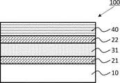
- FIGS. 1 to 3 are cross-sectional views showing an embodiment of the barrier film (100) of the present disclosure.
- the barrier film (100) of FIGS. 1 to 3 has an inorganic oxide layer A (21), an organic coating layer B (31), and an inorganic oxide layer C (22) on a light-transmitting substrate (10).
- the barrier film (100) of FIG. 1 has an organic coating layer D (32) on the opposite side of the inorganic oxide layer C (22) from the organic coating layer B (31).
- the barrier film (100) of FIG. 2 has an organic coating layer D (32) and a primer layer E (40) on the opposite side of the inorganic oxide layer C (22) from the organic coating layer B (31). is doing.
- the barrier film (100) of FIG. 3 has a primer layer E (40) on the opposite side of the inorganic oxide layer C (22) from the organic coating layer B (31).
- the barrier film is required to have a value of water vapor transmission rate according to JIS K7129-2: 2019 of 0.20 g / m 2 ⁇ day or less.
- the barrier film cannot suppress the deterioration of the quantum dots, so that the barrier film has a peak or bottom of spectral transmittance at 450 nm ⁇ 7 nm.
- the change in color cannot be suppressed.
- the water vapor transmission rate is preferably 0.17 g / m 2 ⁇ day or less, more preferably 0.15 g / m 2 ⁇ day or less, and further preferably 0.13 g / m 2 ⁇ day or less. preferable.
- the lower limit of the water vapor transmission rate is not particularly limited, but is usually about 0.05 g / m 2 ⁇ day in consideration of ease of manufacture and cost.
- the temperature and humidity conditions for measuring the water vapor transmission rate are 40 ° C. and 90% relative humidity. Further, before measuring the water vapor transmission rate, the sample for measurement shall be exposed to an atmosphere having a temperature of 23 ° C. ⁇ 5 ° C. and a relative humidity of 40% or more and 65% or less for 30 minutes or more.
- the water vapor transmission rate can be measured by, for example, a water vapor transmission rate measuring device (trade name: PERMATRAN) manufactured by MOCON.
- the water vapor transmission rate can be easily set in the above range by forming at least one of the inorganic oxide layer and the organic coating layer in two or more layers. Further, the water vapor transmission rate can be easily set in the above range by increasing the thickness of the inorganic oxide layer or the organic coating layer.
- the barrier film of the present disclosure has a spectral transmittance in the range of 450 nm ⁇ 7 nm when the spectral transmittance of the barrier film is measured with the surface having the inorganic oxide layer and the organic coating layer as the light incident surface. Is required to have a bottom of spectral transmittance that changes from decrease to increase, or a peak of spectral transmittance that changes from increase to decrease.
- the surface of the barrier film on the side having the inorganic oxide layer and the organic coating layer means the surface on the side having the inorganic oxide layer and the organic coating layer with reference to the light-transmitting substrate.
- the upper surface of FIGS. 1 to 3 is the light incident surface.
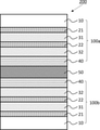
- the barrier films (100a, 100b) are arranged on both sides of the quantum dot-containing layer (50) and are used as constituent members of the wavelength conversion sheet (200).
- the light emitted from the primary light source of the backlight (generally, blue light having a wavelength of 450 nm as the center) is the barrier film (100b) on the lower side of the wavelength conversion sheet (200). ) Is incident on the light-transmitting substrate (10).
- the light of the primary light source When the light of the primary light source is incident on the light transmissive substrate (10) of the barrier film (100b) on the lower side of the wavelength conversion sheet (200) of FIGS. 4 to 6, most of the light is on the lower barrier. It penetrates the film (100b) and reaches the quantum dot-containing layer (50). Then, among the light of the primary light source that has reached the quantum dot-containing layer (50), the light that collides with the quantum dots is converted into light having a wavelength different from that of the primary light source (hereinafter, it collides with the quantum dots and is converted.
- the light is referred to as L2), and is incident on the upper barrier film (100a). Examples of L2 include green light and red light.
- the light that does not collide with the quantum dots is incident on the upper barrier film (100a) as the light of the wavelength of the primary light source.
- the light that does not collide with the quantum dots and is not converted is referred to as L1.
- Examples of L1 include blue light.
- Most of the light (L1 and L2) incident on the upper barrier film (100a) passes through the upper barrier film (100a) and is arranged closer to the viewer than the wavelength conversion sheet (200).
- Toward a member for example, a brightness improving sheet such as a prism sheet).
- the color of the liquid crystal display device to which the wavelength conversion sheet including the barrier film is applied is established by the balance between L1 and L2. Therefore, it is considered that the reason why the color of the liquid crystal display device to which the wavelength conversion sheet is applied changes with time is that the balance between L1 and L2 changes.
- the present inventors have diligently studied the cause of the change in the balance between L1 and L2. First, it is considered that the amount of light of L2 gradually decreases as the quantum dots deteriorate. However, since the deterioration of the quantum dots is suppressed by the presence of the barrier film or the like, the change in color cannot be explained only by the deterioration of the quantum dots. Further, when the primary light source is deteriorated, not only L1 but also L2 is relatively reduced, so that it is unlikely that the deterioration of the primary light source is the cause.
- the present inventors have found that the change in the transmittance of L1 of the upper barrier film 100a ( ⁇ the change in the amount of light of L1 emitted from the upper barrier film) and the amount of light of L2 due to the deterioration of the quantum dots. It was found that the color of the liquid crystal display device to which the wavelength conversion sheet containing the barrier film was applied was changed by the synergistic action of the change. Then, the present inventors mainly cause the transmittance of L1 of the upper barrier film 100a ( ⁇ the amount of light of L1 emitted from the upper barrier film 100a) to change with time due to the swelling of the organic coating layer due to humidity. I found that there is.
- the spectral transmittance of the barrier film has a peak or bottom in the range of 450 nm ⁇ 7 nm indicates that the waveform of the spectral transmittance spectrum of the light transmitted through the barrier film has a peak or bottom in the vicinity of 450 nm. ing.
- the waveform of the spectral transmission spectrum of the barrier film having a peak or a bottom in the vicinity of 450 nm, it is possible to suppress the suppression of the change in color when exposed to a high humidity environment.
- the reason for producing such an effect is considered as follows. First, when the barrier film is exposed to a high humidity environment, the organic coating layer of the barrier film swells.
- the thickness of the organic coating layer increases, so that the waveform of the spectral transmittance of the barrier film shifts (mainly shifts to the long wavelength side).
- the spectral transmittance of the barrier film tends to change little in the vicinity of the peak or the bottom, but increases in the region outside the peak or the bottom. Therefore, by setting the transmittance of the barrier film at a wavelength of 450 nm near the peak or near the bottom, it is possible to suppress a change in the transmittance at 450 nm when the organic coating layer swells and the waveform of the spectral transmission spectrum shifts. it is conceivable that.
- the central wavelength of the primary light of the backlight using the quantum dots is approximately 450 nm, suppressing the change in the transmittance of the barrier film at 450 nm is the result of the light of the primary light source reaching the quantum dot-containing layer (50).
- the change in the transmittance of the light (L1) that did not collide with the quantum dots can be suppressed, and the change in the tint of the backlight using the quantum dots can be suppressed.
- the wavelength region of L2 green and red
- the wavelength region of L2 has a longer period of the waveform of the spectral transmission spectrum than that of L1 (blue), it is not easily affected by the swelling of the organic coating layer.
- the position of the peak or bottom of the spectral transmittance of the barrier film in the range of 450 nm ⁇ 7 nm, it is possible to suppress the change in color when the barrier film is applied to the wavelength conversion sheet. It is thought that it can be done.
- the position of the peak or the bottom is more preferably in the range of 450 nm ⁇ 5 nm, further preferably in the range of 450 nm ⁇ 3 nm, and even more preferably in the range of 450 nm ⁇ 1 nm.
- the spectral transmittance is preferably measured with the measurement wavelength interval set to 1 nm.
- Examples of the device for measuring the spectral transmittance include an ultraviolet-visible spectrophotometer (model number: V-670) manufactured by JASCO Corporation.
- temperature when measuring various parameters such as spectral transmittance, total light transmittance, tint (x value and y value of Yxy color system), thickness of each layer, etc., unless otherwise specified, temperature is used.
- the measurement shall be performed in an atmosphere of 23 ° C. ⁇ 5 ° C. and a relative humidity of 40% or more and 65% or less.
- the sample shall be exposed to the atmosphere for at least 30 minutes before measuring various parameters.
- Adjustment method of peak or bottom position a method for adjusting the position of the peak or the bottom will be described.
- the reason why the value of the spectral transmittance differs depending on the wavelength is mainly due to the thin film interference of the laminated body.
- a method for adjusting the position of the peak or the bottom by thin film interference will be described using the wavelength conversion sheet of FIG. 4 as an example.
- L1 light of the primary light source that has reached the quantum dot-containing layer (50) and does not collide with the quantum dots
- the six interfaces are the interface between the quantum dot-containing layer and the organic coating layer D (interface 1), the interface between the organic coating layer D and the inorganic oxide layer C (interface 2), the inorganic oxide layer C and the organic coating layer B.
- Interface (interface 3) interface between organic coating layer B and inorganic oxide layer A (interface 4), interface between inorganic oxide layer A and light-transmitting substrate (interface 5), light-transmitting substrate
- the refractive index n Z of the quantum dot-containing layer is usually smaller than the refractive index n D of the organic coating layer D. Therefore, the reflection at interface 1 is usually a fixed end reflection.
- the transmittance (%) of L1 is generally "100 (%) -reflectance (%)". Then, the reflectance of L1 needs to consider the interference between the reflection of the interface 1 and the reflection of another interface. Specifically, when the reflection of the interface 1 is reduced by the interference with the reflection of another interface, the transmittance of L1 becomes high, and conversely, the reflection of the interface 1 is reduced by the interference with the reflection of the other interface. When it increases, the transmittance of L1 decreases.
- the refractive index n A of the inorganic oxide layer A and the refractive index n C of the inorganic oxide layer C are the refractive index n B of the organic coating layer B and the refractive index n of the organic coating layer D.
- the reflection at the interface 2 is the fixed end reflection
- the reflection at the interface 3 is the free end reflection
- the reflection at the interface 4 is the fixed end reflection.
- the barrier property tends to be good even if the thickness of the inorganic oxide layer is thin, so that the thickness of the inorganic oxide layer is usually thin. design. Therefore, the optical distance in the fixed end reflection of the interface 2 and the optical distance in the free end reflection of the interface 3 can be regarded as substantially the same. Further, since usually n A ⁇ n C and n B ⁇ n D , the reflectances of the interface 2 and the interface 3 are substantially the same. Therefore, it can be considered that the fixed-end reflection of the interface 2 and the free-end reflection of the interface 3 cancel each other out and do not affect the fixed-end reflection of the interface 1.
- the refractive index nA of the inorganic oxide layer A is higher than the refractive index n0 of the light transmissive substrate.
- the reflection at the interface 5 is a free end reflection.
- the optical distance in the fixed end reflection of the interface 4 and the freedom of the interface 5 are usually designed to reduce the thickness of the inorganic oxide layer. It can be regarded as substantially the same as the optical distance in the edge reflection.
- the reflectance of the interface 4 and the reflectance of the interface 5 are compared, and the reflection of the interface having the higher reflectance affects the fixed-end reflection of the interface 1.
- the reflectance of the interface (interface 4) between the inorganic oxide layer A and the organic coating layer B is larger than the reflectance of the interface (interface 5) between the light-transmitting substrate and the inorganic oxide layer A.
- the interface 5 is not considered as the reflection that affects the fixed-end reflection of the interface 1, but the interface 4 is considered.
- the reflection of the interface 6 is examined.
- the thickness of the light-transmitting substrate is designed to be sufficiently thicker than the wavelength of light.
- the reflection at the interface 6 is a reflection that can be ignored as so-called thin film interference.
- the reflection that should be considered as the reflection that interferes with the reflection of the interface 1 is the fixed end reflection of the interface 4.
- reflections other than the interface 4 also have a slight effect on the reflection of the interface 1.
- only the reflection of the interface 4 affects the reflection of the interface 1.
- the reflection of the interface 4 is the reflection of the interface 1 when the relationship of the following formula m-1 is satisfied for the light having the wavelength ⁇ . And the reflectance is reduced. And, the decrease of the reflectance means that the transmittance increases. Therefore, assuming that the reflections at the interface 1 and the interface 4 are both fixed-end reflections, the light having a wavelength ⁇ emitted from the quantum dot-containing layer is transmitted when the relationship of the following equation m-1 is satisfied. The rate is the highest. In the above example, it is assumed that the thicknesses of the inorganic oxide layer A and the inorganic oxide layer C are thin enough not to affect the interference.
- Equation m-1 can be transformed into the following equation m-2.
- n B x t B + n D x t D ⁇ / 4 (Equation m-2)
- “D 1 ” in the following formula m-3 indicates how many times “n B ⁇ t B + n D ⁇ t D ” is “112.5 nm”.
- d 1 n B ⁇ t B / 112.5 nm + n D ⁇ t D / 112.5 nm (Equation m-3) Then, assuming that the reflections of the interface 1 and the interface 4 are both fixed-end reflections, when d 1 of the equation m-3 is 2x + 1 (x is an integer of 0 or more), light having a wavelength of 450 nm is obtained.
- the spectral transmittance has a peak or bottom in the range of 450 nm ⁇ 7 nm. It can be easily adjusted. Further, in the above example, when d 1 of the equation m-3 is near an odd integer, the peak or the bottom becomes a peak in which the spectral transmittance changes from an increase to a decrease. Further, in the above example, when d 1 of the equation m-3 is near an even integer, the peak or the bottom becomes the bottom where the spectral transmittance changes from decreasing to increasing.
- D 1 of the formula m-3 does not have to be an integer, and if it is an integer of about ⁇ 0.10, the position of the peak or the bottom can be easily adjusted in the range of 450 nm ⁇ 7 nm. Further, in the case of the above example, when d 1 of the equation m-3 is in the range of an integer to an integer + 0.10, the peak position can be easily adjusted to 450 nm or more and 457 nm or less, and the integer is ⁇ 0.10 to an integer. In the case of the range of, it is easy to adjust the position of the bottom to 443 nm or more and 450 nm or less. As described above, in reality, reflections other than the interface 4 also have a slight effect on the reflections at the interface 1. Therefore, in the above case, it is preferable to carry out the basic design by the above method and make minor corrections by the simulation of the reflection spectrum. For the simulation of the reflection spectrum, general-purpose simulation software can be used.
- the reflection of the interface 1 is usually a fixed end reflection, but when the reflection of the interface 1 is a free end reflection, it may be considered as follows.
- the reflection to be considered as the reflection that interferes with the reflection of the interface 1 which is the free end reflection is still the fixed end reflection of the interface 4.
- d 1 of the formula m-3 is 2x + 1 (x is an integer of 0 or more)
- the transmittance at a wavelength of 450 nm is the lowest
- d 1 of the formula m-3 is 2x (x is 1).
- the above integer the transmittance at a wavelength of 450 nm is the highest.
- the barrier film has the primer layer E on the opposite side of the organic coating layer D from the inorganic oxide layer C will be examined.
- L1 light of the primary light source that reached the quantum dot-containing layer (50) and did not collide with the quantum dots
- L1 light of the primary light source that reached the quantum dot-containing layer (50) and did not collide with the quantum dots
- the seven interfaces are the interface between the quantum dot-containing layer and the primer layer E (interface 1-1), the interface between the primer layer E and the organic coating layer D (interface 1-2), the organic coating layer D and the inorganic oxide layer.
- Interface with C interface 2
- interface between inorganic oxide layer C and organic coating layer B interface 3
- interface between organic coating layer B and inorganic oxide layer A interface 4
- inorganic oxide layer A The interface between the light-transmitting base material and the light-transmitting base material (interface 5), and the interface between the light-transmitting base material and air (interface 6).
- the refractive index n Z of the quantum dot-containing layer is usually smaller than the refractive index n E of the primer layer E. Therefore, the reflection at interface 1-1 is usually a fixed end reflection. In examining the interference between the reflection of interface 1-1 (usually fixed-end reflection) and the reflection of interface 1-2, 2 to 6, it is necessary to examine the nature of the reflection of interface 1-2, 2 to 6.
- the reflection at the interface 1-2 is considered to be a fixed end reflection or a free end reflection.
- the refractive index n E of the primer layer E and the refractive index n D of the organic coating layer D are designed so that the difference in refractive index is small. To. Therefore, the reflection at the interface 1-2 having a low reflectance can be ignored. It can be considered that the reflection of the interface 2 and the reflection of the interface 3 cancel each other out and do not affect the fixed end reflection of the interface 1-1 as in the case of not having the primer layer E.
- the relationship between the reflection at the interface 4 and the reflection at the interface 5 will be examined assuming that the interface 4 has a higher reflectance, as in the above case.
- the reflection of the interface 5 is not considered, but the reflection of the interface 4 is considered.
- the reflection at the interface 6 is a reflection that can be ignored as so-called thin film interference. Therefore, the reflection that should be considered as the reflection that interferes with the reflection of the interface 1-1 (usually the fixed end reflection) is the fixed end reflection of the interface 4.
- the optical distance ( nE ⁇ tE ) of the primer layer is the optical distance of the fixed end reflection of the interface 4. (In the above case as well, in reality, reflections other than interface 4 also have a slight effect on the reflection of interface 1-1. However, here, for the sake of brevity, only the reflection of interface 4 is interface 1-. It is explained as affecting the reflection of 1.)
- the reflection of the interface 4 is the interface 1 when the relationship of the following equation n-1 is satisfied for the light having the wavelength ⁇ . It weakens the reflection of -1 and reduces the reflectance. And, the decrease of the reflectance means that the transmittance increases. Therefore, assuming that the reflections at the interface 1-1 and the interface 4 are both fixed-end reflections, the light having a wavelength ⁇ emitted from the quantum dot-containing layer satisfies the relationship of the following equation n-1. , The transmittance is the highest. In the above example, it is assumed that the thickness of the inorganic oxide layer A and the inorganic oxide layer C is thin enough not to affect the interference.
- Equation n-1 can be transformed into the following equation n-2.
- n B x t B + n D x t D + n E x t E ⁇ / 4 (Equation n-2)
- n B ⁇ t B + n D ⁇ t D the transmittance of the wavelength ⁇ is the highest even when "+ n E x t E " is an odd multiple of " ⁇ / 4”. Then, how many times "n B ⁇ t B + n D ⁇ t D + n E ⁇ t E " is multiplied by " ⁇ / 4" can be calculated by dividing the left side of the equation n-2 by the right side.
- the central wavelength of the primary light of the backlight using quantum dots is approximately 450 nm.
- ⁇ is 450 nm
- “ ⁇ / 4” in the formula n-2 is “112.5 nm”.
- “ ⁇ / 4" of the formula n-2 is "112.5 nm”
- dividing the left side of the formula n-2 by the right side gives the following formula n-3.
- “D 2 ” in the following equation n-3 indicates how many times “n B ⁇ t B + n D ⁇ t D + n E ⁇ t E ” is “112.5 nm”.
- d 2 n B ⁇ t B / 112.5 nm + n D ⁇ t D / 112.5 nm + n E ⁇ t E / 112.5 nm (Equation n-3)
- d 2 of the equation n-3 2y + 1 (y is an integer of 0 or more)
- the wavelength is 450 nm.
- d 2 of the formula n-3 2y (y is an integer of 1 or more)
- the transmittance of light having a wavelength of 450 nm is the lowest.
- Light having a wavelength of 450 nm can be regarded as L1 described above.
- the spectral transmittance peak or bottom is provided in the range of 450 nm ⁇ 7 nm. It can be easily adjusted. Further, in the above example, when d 2 of the equation n-3 is near an odd integer, the peak or the bottom becomes a peak in which the spectral transmittance changes from an increase to a decrease. Further, in the above example, when d 2 of the equation n-3 is near an even integer, the peak or the bottom becomes the bottom where the spectral transmittance changes from decreasing to increasing.
- D 2 of the formula n-3 does not have to be an integer, and if it is an integer of about ⁇ 0.10, the position of the peak or the bottom can be easily adjusted in the range of 450 nm ⁇ 7 nm. Further, in the case of the above example, when d 2 of the formula m-3 is in the range of an integer to an integer + 0.10, the peak position can be easily adjusted to 450 nm or more and 457 nm or less, and the integer is ⁇ 0.10 to an integer. In the case of the range of, it is easy to adjust the position of the bottom to 443 nm or more and 450 nm or less.
- the reflection of the interface 1-1 is usually a fixed end reflection, but when the reflection of the interface 1-1 is a free end reflection, it may be considered as follows. In this case, the reflection to be considered as the reflection that interferes with the reflection of the interface 1-1, which is the free end reflection, is still the fixed end reflection of the interface 4.
- d 2 of the formula n-3 is 2y + 1 (y is an integer of 0 or more)
- the transmittance at a wavelength of 450 nm is the lowest
- d 2 of the formula n-3 is 2y (y is 1). The above integer)
- the transmittance at a wavelength of 450 nm is the highest.
- the position of the peak or bottom of the spectral transmittance of the barrier film can be adjusted by considering the action of thin film interference based on the refractive index and thickness of each layer.
- a polyethylene terephthalate film generally used as a light-transmitting substrate was used, and an inorganic oxide layer having a low refractive index and a thick thickness was used.
- the interface between the inorganic oxide layer and the light-transmitting substrate usually exhibits the highest reflectance.
- the reflection that interferes with the reflection at the interface between the quantum dot-containing layer and the barrier film may mainly consider the reflection at the interface between the inorganic oxide layer and the light-transmitting substrate.
- the peak or bottom is preferably a peak in which the spectral transmittance changes from an increase to a decrease.
- the central wavelength of the primary light source of the backlight using the quantum dots is approximately 450 nm. Therefore, the peak or bottom in the range of 450 nm ⁇ 7 nm is the peak at which the spectral transmittance changes from increasing to decreasing, so that the light of the primary light source that has reached the quantum dot-containing layer does not collide with the quantum dots ( It is preferable in that the transmittance of L1) can be increased.
- the inorganic oxide layer is a layer containing silicon oxide, the L * a * b * color system b * value of the barrier film tends to increase.
- the peak or bottom in the range of 450 nm ⁇ 7 nm is the peak at which the spectral transmittance changes from increase to decrease, so that even if the inorganic oxide layer is a layer containing silicon oxide, the yellowish color of the barrier film can be obtained. It is preferable because it is easy to suppress.
- the peak or the bottom is a peak in which the spectral transmittance changes from an increase to a decrease
- the transmittance at a wavelength of 450 nm decreases when the organic coating layer swells and the waveform of the spectral reflectance of the barrier film shifts to the long wavelength side. .. That is, in the barrier film having a peak at a position of 450 nm or more and 457 nm or less, the transmittance of L1 decreases when the organic coating layer swells.
- the amount of light (L2) converted by the quantum dots gradually decreases due to the deterioration of the quantum dots. Therefore, in the barrier film having a peak at a position of 450 nm or more and 457 nm or less, the amount of light of L2 decreases due to the deterioration of the quantum dots, and the transmittance of L1 also decreases, so that the balance between L1 and L2 is less likely to be lost, and the color It is preferable in that the change in taste can be further suppressed.
- the peak or bottom is a bottom in which the spectral transmittance changes from a decrease to an increase, and it is also preferable to have a bottom with a spectral transmittance of 443 nm or more and 450 nm or less.
- the transmittance at a wavelength of 450 nm decreases when the organic coating layer swells and the waveform of the spectral reflectance of the barrier film shifts to the long wavelength side. .. That is, in the barrier film having the bottom at a position of 443 nm or more and 450 nm or less, the transmittance of L1 decreases when the organic coating layer swells.
- the amount of light (L2) converted by the quantum dots gradually decreases due to the deterioration of the quantum dots. Therefore, in the barrier film having the bottom at a position of 443 nm or more and 450 nm or less, the amount of light of L2 decreases due to the deterioration of the quantum dots, and the transmittance of L1 also decreases, so that the balance between L1 and L2 is less likely to be lost, and the color It is preferable in that the change in taste can be further suppressed.
- the barrier film of the present disclosure has at least one inorganic oxide layer and at least one organic coating layer on one surface of a light-transmitting substrate, and has the above-mentioned water vapor permeability and spectral transmittance.
- the layer structure is not particularly limited as long as it satisfies the above conditions.
- the barrier film preferably has a laminated structure having two or more inorganic oxide layers and at least one organic coating layer on one surface of a light-transmitting base material. Further, the barrier film has two or more inorganic oxide layers and at least one organic coating layer on one surface of the light-transmitting substrate from the viewpoint of barrier property and adhesion to the quantum dot-containing layer. , It is more preferable to have a laminated structure having a primer layer. As in these preferred embodiments, when the number of layers of the inorganic oxide layer and the organic coating layer arranged on the light-transmitting substrate increases and the thickness increases, the period of the spectral transmittance waveform becomes shorter. Therefore, it is possible to easily exert the effect by setting the peak or bottom to the vicinity of 450 nm.
- Examples of the layer structure of the barrier film of the present disclosure include the following structures (1) to (3).
- "/" means the interface of the layer.
- the following configurations (1) to (3) are preferable in that they have excellent barrier properties. Above all, the following configurations (2) to (3) are preferable in that they have excellent adhesion to the quantum dot-containing layer. Further, in the following configurations (1) to (3), the number of layers of the light-transmitting base material is small (for example, one layer of an inorganic oxide layer and one layer of organic matter are placed on the light-transmitting base material.
- the layer structure of (1) to (3) may have other functional layers such as a light diffusion layer on the surface of the light transmissive substrate opposite to the inorganic oxide layer A.
- the barrier film may have a layer other than the above as long as the effect of the present disclosure is not impaired.
- the barrier film of the present disclosure also includes the configurations of (4) and (5) below.
- the laminated structure of the following (4) and (5) is disadvantageous in terms of optical characteristics because the number of interfaces is larger than that of the above (2) and (3), and the total thickness also increases. .. Therefore, the laminated structure of the above (1) to (3) is preferable.
- the inorganic oxide layer A as the inorganic oxide layer, the organic coating layer B as the organic coating layer, and the inorganic as the inorganic oxide layer are obtained on one surface of the light-transmitting base material. It has an oxide layer C and an organic coating layer D as the organic coating layer in this order.
- the inorganic oxide layer A, the organic coating layer B, the inorganic oxide layer C and the organic coating layer D are in contact with each other. Further, it is preferable that the light-transmitting substrate and the inorganic oxide layer A are in contact with each other.
- the above (2) has a configuration in which the primer layer E is further provided on the organic coating layer D of the above (1). In the above (2), it is preferable that the organic coating layer D and the primer layer E are in contact with each other.
- the inorganic oxide layer A as the inorganic oxide layer, the organic coating layer B as the organic coating layer, and the inorganic as the inorganic oxide layer are obtained on one surface of the light-transmitting base material. It has an oxide layer C and a primer layer E in this order.
- the inorganic oxide layer A, the organic coating layer B, the inorganic oxide layer C and the primer layer E are in contact with each other. Further, it is preferable that the light-transmitting substrate and the inorganic oxide layer A are in contact with each other.
- the total thickness of the inorganic oxide layer and the organic coating layer is preferably 150 nm or more and 1500 nm or less, more preferably 200 nm or more and 800 nm or less, and further preferably 300 nm or more and 650 nm or less.
- the barrier property can be easily improved.
- the total thickness is possible to suppress the period of the spectral transmittance waveform from becoming too short, and to exert the effect of having the peak or bottom of the spectral transmittance in the range of 450 nm ⁇ 7 nm. It can be done easily.
- the total thickness of the inorganic oxide layer, the organic coating layer and the primer layer is preferably 300 nm or more and 1700 nm or less, more preferably 400 nm or more and 900 nm or less, further preferably 450 nm or more and 800 nm or less, and further preferably 500 nm or more. It is more preferably 750 nm or less.
- the barrier property can be easily improved.
- the total thickness it is possible to suppress the period of the spectral transmittance waveform from becoming too short, and to exert the effect of having the peak or bottom of the spectral transmittance in the range of 450 nm ⁇ 7 nm. It can be done easily.
- the light-transmitting substrate is not particularly limited as long as it is a resin film that does not impair the function of the wavelength conversion sheet when applied to the wavelength conversion sheet.
- Examples of the light-transmitting substrate include polyester, triacetyl cellulose (TAC), cellulose diacetate, cellulose acetate butyrate, polyamide, polyimide, polyether sulphon, polysulphon, polypropylene, polymethylpentene, polyvinyl chloride, and polyvinyl acetal.
- Examples thereof include a resin film formed of one or more resins selected from polyether ketone, acrylic, polycarbonate, polyurethane, amorphous olefin (Cyclo-Olfin-Polymer: COP) and the like.
- a stretched polyester film particularly a biaxially stretched polyester film, is preferable from the viewpoint of mechanical strength, dimensional stability and heat resistance.
- the polyester film include polyethylene terephthalate film and polyethylene naphthalate film.
- the light-transmitting substrate may be a single layer of a resin film or may have a plurality of resin films. When having a plurality of resin films, each resin film may be directly bonded or may be bonded via an adhesive layer.
- the thickness t 0 of the light-transmitting substrate is preferably 5 ⁇ m or more, more preferably 8 ⁇ m or more, and further preferably 10 ⁇ m or more.
- the thickness of the light-transmitting substrate is preferably 5 ⁇ m or more, more preferably 8 ⁇ m or more, and further preferably 10 ⁇ m or more.
- the thickness t 0 of the light-transmitting substrate is preferably 200 ⁇ m or less, more preferably 150 ⁇ m or less, from the viewpoint of thinning and facilitating the suppression of invasion of water vapor and oxygen from the end portion. It is more preferably 100 ⁇ m or less, more preferably 50 ⁇ m or less, and even more preferably 25 ⁇ m or less.
- the thickness of each layer constituting the barrier film such as the thickness t 0 of the light transmissive substrate and the thickness of the quantum dot-containing layer are photographed by using, for example, a scanning transmission electron microscope (STEM). It can be calculated from the average value of the values at 20 points by measuring the thickness at 20 points from the image of the cross section.
- STEM scanning transmission electron microscope
- a numerical range For example, in the case of the thickness t 0 of the light transmissive substrate, embodiments in a numerical range such as 5 ⁇ m or more and 200 ⁇ m or less, 5 ⁇ m or more and 25 ⁇ m or less, 8 ⁇ m or more and 50 ⁇ m or less, 10 ⁇ m or more and 50 ⁇ m or less, 10 ⁇ m or more and 25 ⁇ m or less can be mentioned. ..
- the thickness of the first resin film on the side where the inorganic oxide layer or the like is formed is preferably 5 ⁇ m or more and 50 ⁇ m or less, and 8 ⁇ m or more and 25 ⁇ m or less. It is more preferably 10 ⁇ m or more and 20 ⁇ m or less.
- the first resin film has the above thickness, the production efficiency of the inorganic oxide layer can be easily improved and the handleability can be easily improved.
- the thickness of the second resin film on the side far from the inorganic oxide layer or the like is preferably 5 ⁇ m or more and 150 ⁇ m or less, more preferably 8 ⁇ m or more and 100 ⁇ m or less, and further preferably 10 ⁇ m or more and 50 ⁇ m or less.
- the second resin film has the above thickness, it is possible to easily improve the balance between the handleability and the rigidity of the barrier film.
- the light-transmitting base material is composed of two resin films, the two resin films may be bonded to each other via an adhesive layer, and then an inorganic oxide layer or the like may be formed, or the first resin film may be formed.
- the second resin film may be attached to the surface of the first resin film opposite to the inorganic oxide layer or the like via the adhesive layer.
- the thickness of the adhesive layer is preferably 3 ⁇ m or more and 100 ⁇ m or less, more preferably 3 ⁇ m or more and 50 ⁇ m or less, and further preferably 4 ⁇ m or more and 8 ⁇ m or less. If the thickness of the adhesive layer is too thin, coating defects may occur, and if the thickness is too thick, curing may be insufficient.
- the light transmittance of JIS K7361-1: 1997 is preferably 80% or more, more preferably 85% or more, and further preferably 87% or more.
- the surface of the light-transmitting base material on the side where the inorganic oxide layer or the like is provided may be previously subjected to a desired surface treatment in order to improve adhesion or the like.
- a desired surface treatment examples include corona discharge treatment, ozone treatment, low temperature plasma treatment using oxygen gas or nitrogen gas, glow discharge treatment, oxidation treatment using chemicals and the like.
- the barrier film of the present disclosure has an inorganic oxide layer on a light-transmitting substrate.
- the inorganic oxide layer mainly has an action of improving the barrier property.
- the inorganic oxide layer on the light-transmitting substrate may be only one layer, but it is preferable to have two layers. Although the inorganic oxide layer may have three or more layers, two layers are preferable from the viewpoint of cost effectiveness. In the present specification, the two inorganic oxide layers on the light-transmitting substrate are referred to as an inorganic oxide layer A and an inorganic oxide layer C.
- the barrier property of the barrier film against oxygen and water vapor can be improved, and the deterioration of the quantum dots can be easily suppressed.
- the thickness of the inorganic oxide layer becomes thick and cracks are likely to occur in the inorganic oxide layer, so that the barrier property is good over a long period of time. It becomes difficult to do.
- a predetermined barrier property can be imparted as a laminated body as long as the positions of the cracks and pinholes do not match in the plane direction. That is, it is preferable to use two inorganic oxide layers because it is easy to impart a predetermined barrier property even when cracks or pinholes occur in the inorganic oxide layer.
- the inorganic oxide layer A and the inorganic oxide layer C can exemplify a layer made of one selected from aluminum oxide, magnesium oxide, indium tin oxide (ITO), and silicon oxide, or a mixture thereof.
- the composition and various physical properties of the inorganic oxide layer A and the inorganic oxide layer C may be the same or different. Considering the balance of the physical properties of the barrier film, it is preferable that at least a part of the composition and various physical properties of the inorganic oxide layer A and the inorganic oxide layer C are substantially the same.
- the refractive index n A of the inorganic oxide layer A and the refractive index n C of the inorganic oxide layer C are substantially the same.
- the fact that n A and n C are substantially the same means that n A / n C is 0.98 or more and 1.02 or less, preferably 0.99 or more and 1.01 or less, and more preferably. It is 1.00.
- the thickness t A of the inorganic oxide layer A and the thickness t C of the inorganic oxide layer C are substantially the same.
- the fact that t A and t C are substantially the same means that t A / t C is 0.95 or more and 1.05 or less, preferably 0.97 or more and 1.03 or less, and more preferably. It is 0.99 or more and 1.01 or less.
- Inorganic oxide layers with a high refractive index tend to have good barrier properties.
- aluminum oxide has a high refractive index and a good barrier property. Therefore, by using aluminum oxide as the inorganic oxide layer A and the inorganic oxide layer C, it becomes easy to impart a predetermined barrier property even if the thickness of the inorganic oxide layer is reduced, so that the spectral transmission of the barrier film is possible.
- the inorganic oxide layer can be easily thinned to a level that has almost no effect on the waveform of the spectrum, and the transparency can be improved.
- the inorganic oxide layer A and the inorganic oxide layer C are preferably layers containing aluminum oxide or silicon oxide from the viewpoint of transparency and productivity. Further, at least one of the inorganic oxide layer A and the inorganic oxide layer C is preferably a layer containing aluminum oxide from the viewpoint of sufficient barrier property, transparency, productivity and the like, and the inorganic oxide layer A and the inorganic oxide layer C are preferable. It is more preferable that both of the inorganic oxide layers C are layers containing aluminum oxide.
- the content ratio of aluminum oxide or silicon oxide in the inorganic oxide layer A or the inorganic oxide layer C is preferably 80% by mass or more, more preferably 90% by mass or more, and 95% by mass or more on a mass basis. Is more preferable.
- Examples of the embodiment of the combination of the inorganic oxide layer A and the inorganic oxide layer C include the following (1) to (4).
- the inorganic oxide layer A is a layer containing silicon oxide.
- the embodiment in which the inorganic oxide layer C is a layer containing aluminum oxide.
- the thickness t A of the inorganic oxide layer A and the thickness t C of the inorganic oxide layer C are used as the material of the inorganic oxide layer so as to have a good balance between barrier properties, scratch suppression, and crack suppression. It is preferable to set the range appropriately. Although t A and t C may be different from each other, it is preferable that t A and t C are substantially the same as described above.
- t A and t C each have a lower limit of 6 nm or more, and more preferably 7 nm or more. preferable.
- the upper limit of t A and t C is preferably 25 nm or less, more preferably 20 nm or less, more preferably 15 nm or less, still more preferably 12 nm or less, and more preferably 10 nm or less. Is more preferable.
- the thickness of the inorganic oxide layer A and the inorganic oxide layer C is preferably 12 nm or less, more preferably 10 nm or less).
- t A and t C each have a lower limit of 20 nm.
- the above is preferable, 25 nm or more is more preferable, and 27 nm or more is more preferable.
- the barrier property can be easily improved.
- the upper limit of t A and t C is preferably 100 nm or less, more preferably 75 nm or less, further preferably 60 nm or less, still more preferably 50 nm or less.
- a physical vapor deposition method such as a vacuum vapor deposition method, a sputtering method, and an ion plating method, or a plasma chemical vapor deposition method, a thermochemical vapor deposition method, and a photochemical vapor deposition method can be used. It can be formed by a chemical vapor deposition method or the like. Among these, the vacuum vapor deposition method having a high vapor deposition rate and good productivity is preferable.
- the barrier film of the present disclosure has an organic coating layer.
- the barrier property of the barrier film can be improved and the deterioration of the quantum dots can be easily suppressed.
- the organic coating layer has better flexibility than the inorganic oxide layer, the organic coating layer can easily suppress the generation of scratches and cracks in the inorganic oxide layer.
- the organic coating layer is preferably formed in contact with the inorganic oxide layer.
- the organic coating layer on the light-transmitting substrate may be only one layer, but preferably has two layers.
- the organic coating layer may have three or more layers, but one layer or two layers is preferable from the viewpoint of cost effectiveness.
- the organic coating layer B when a light-transmitting substrate has one organic coating layer, the organic coating layer is referred to as an organic coating layer B.
- the organic coating layer B when two organic coating layers are provided on the light-transmitting base material, the organic coating layer on the side closer to the light-transmitting base material is referred to as the organic coating layer B, and the organic coating on the side farther from the light-transmitting base material.
- the layer is referred to as an organic coating layer D.
- the organic coating layer preferably contains at least one selected from a water-soluble polymer and a metal alkoxide-based compound. Further, the organic coating layer more preferably contains at least one selected from the water-soluble polymer among the water-soluble polymer and the metal alkoxide-based compound, and one or more selected from the water-soluble polymer and the metal alkoxide. It is more preferable to include one or more selected from the system compounds.
- the water-soluble polymer examples include polyvinyl alcohol, polyvinylpyrrolidone, and an ethylene-vinyl alcohol copolymer.
- polyvinyl alcohol and ethylene-vinyl alcohol copolymer are preferable, and polyvinyl alcohol is more preferable, from the viewpoint of barrier property. That is, the organic coating layer preferably contains one or more selected from polyvinyl alcohol and an ethylene-vinyl alcohol copolymer, and more preferably contains polyvinyl alcohol.
- the content of the water-soluble polymer is 5 parts by mass or more and 500 parts by mass or less with respect to 100 parts by mass of the total amount of the metal alkoxide compound. Is more preferable, and it is more preferably 7 parts by mass or more and 100 parts by mass or less, and further preferably 8 parts by mass or more and 50 parts by mass or less.
- metal alkoxide compound examples include metal alkoxide, metal alkoxide hydrolyzate and metal alkoxide polymer.
- the metal alkoxide is a compound represented by the general formula of M (OR) n .
- M represents a metal such as Si, Ti, Al and Zr
- R represents an alkyl group such as a methyl group and an ethyl group.
- Specific examples of the metal alkoxide include tetramethoxysilane, tetraethoxysilane, isopropoxyaluminum and the like.
- the organic coating layer can be formed, for example, by applying a coating liquid containing components constituting the organic coating layer on the inorganic oxide layer and drying it.
- the coating liquid may contain additives such as a silane coupling agent, a curing agent and a dispersant.
- the composition and various physical properties of the organic coating layer B and the organic coating layer D may be the same or different. Considering the balance of the physical properties of the barrier film, it is preferable that at least a part of the organic coating layer B and the organic coating layer D have substantially the same composition and various physical properties.
- the refractive index n B of the organic coating layer B and the refractive index n D of the organic coating layer D are substantially the same.
- the fact that n B and n D are substantially the same means that n B / n D is 0.98 or more and 1.02 or less, preferably 0.99 or more and 1.01 or less, and more preferably. It is 1.00.
- the thickness t B of the organic coating layer B and the thickness t D of the organic coating layer D are substantially the same.
- the fact that t B and t D are substantially the same means that t B / t D is 0.95 or more and 1.05 or less, preferably 0.97 or more and 1.03 or less, and more preferably. It is 0.99 or more and 1.01 or less.
- the lower limit of the refractive index n B of the organic coating layer B and the refractive index n D of the organic coating layer D are preferably 1.45 or more, more preferably 1.50 or more, and 1.52 or more, respectively. Is more preferable. Further, the upper limits of n B and n D are preferably 1.64 or less, more preferably 1.60 or less, and further preferably 1.57 or less, respectively. Even when the organic coating layer is one layer, the refractive index is preferably in the above range.
- the lower limit of the thickness t B of the organic coating layer B and the thickness t D of the organic coating layer D is preferably 70 nm or more, more preferably 85 nm or more, still more preferably 100 nm or more. ..
- the upper limit of t B and t D is preferably 480 nm or less, more preferably 400 nm or less, and further preferably 300 nm or less.
- t B and t D are too thick, the stress generated when the organic coating layer is applied and dried becomes large, and the stress may cause cracks in the inorganic oxide layer and reduce the barrier property. Therefore, by setting t B and t D to 480 nm or less, the initial barrier property can be easily improved. Even when the organic coating layer is one layer, the thickness is preferably in the above range.
- the barrier film may have a primer layer (primer layer E) in addition to the inorganic oxide and the organic coating layer.
- the primer layer is preferably arranged on the outermost layer of the barrier film.
- the refractive index n E of the primer layer E is not particularly limited, but the lower limit is preferably 1.47 or more, more preferably 1.52 or more, and further preferably 1.55 or more. Further, the upper limit of n E is preferably 1.66 or less, more preferably 1.62 or less, and further preferably 1.60 or less.
- the thickness t E of the primer layer E is preferably 70 nm or more and 1000 nm or less, more preferably 100 nm or more and 500 nm or less, and further preferably 120 nm or more and 300 nm or less.
- the primer layer E preferably contains a resin component such as a polyurethane-based resin composition.
- the polyurethane resin easily improves the adhesion to the quantum dot-containing layer, and alleviates the stress generated when the quantum dot-containing layer is ionizing and radiation-cured or thermosetting, and the stress is applied to the inorganic oxide layer and the organic coating. It plays a role in making it difficult to convey to the layers. Further, the polyurethane resin can easily suppress the occurrence of cracks in the layer constituting the barrier film such as the inorganic oxide layer by improving the elongation degree of the primer layer E.
- Examples of the polyurethane-based resin composition include a one-component or two-component polyurethane-based resin composition obtained by reacting a polyfunctional isocyanate with a hydroxyl group-containing compound. Only one kind of the polyfunctional isocyanate and the hydroxyl group-containing compound may be used, or a plurality of kinds may be used.
- examples of the polyfunctional isocyanate include aromatic polyisocyanates such as tolylene diisocyanate, diphenylmethane diisocyanate, xylylene diisocyanate, and polymethylene polyphenylene polyisocyanate, and aliphatic polyisocyanates such as hexamethylene diisocyanate and isophorone diisocyanate.
- hydroxyl group-containing compound examples include polyether polyols, polyester polyols, polyester polyurethane polyols, and polyacrylate polyols.
- a polyester polyurethane polyol is particularly preferable from the viewpoint of adhesion to the quantum dot-containing layer and durability.
- the polyester polyurethane polyol can be produced, for example, by the methods described in JP-A-2001-288408 and JP-A-2003-26996.
- the content of the polyurethane resin composition is preferably 40% by mass or more, more preferably 70% by mass or more, based on the total amount of the primer layer E.
- the primer layer E may further contain a silane coupling agent.
- a silane coupling agent By containing the silane coupling agent, the adhesion between the primer layer E and the organic coating layer D can be easily improved.
- a silane coupling agent a functional group at one end of the molecule, usually a chloro, alkoxy, or acetoxy group, is hydrolyzed to form a silanol group (Si-OH).
- Si-OH silanol group
- the resin composition of the primer layer E is modified by a covalent bond or the like to form a strong bond.
- primer layer E and the organic coating layer D, and the primer layer E and the quantum dot-containing layer are made of an organic functional group such as vinyl, methacryloxy, amino-based, epoxy-based, or mercapto at the other end of the silane coupling agent. It is possible to easily improve the adhesion with.
- silane coupling agent examples include ⁇ -chloropropyltrimethoxysilane, vinyltrichlorosilane, vinyltriethoxysilane, vinyl-tris ( ⁇ -methoxyethoxy) silane, ⁇ -methacryloxypropyltrimethoxysilane, and ⁇ - (3).
- the content of the silane coupling agent is preferably 1% by mass or more, more preferably 3% by mass or more, based on the total amount of the primer layer E.
- the content of the silane coupling agent is within the above range, the adhesion between the primer layer E and the organic coating layer D and the primer layer E and the quantum dot-containing layer can be further improved.
- the content of the silane coupling agent shall be 30% by mass or less based on the total amount of the primer layer E. Is preferable, and 20% by mass or less is more preferable.
- the primer layer E may further contain a filler.
- the filler has a role of adjusting the viscosity of the coating liquid for forming the primer layer and improving the coating suitability and the like.
- the filler for example, calcium carbonate, barium sulfate, alumina white, silica, talc, glass frit, resin powder and the like can be used.
- the primer layer may further contain additives such as stabilizers, cross-linking agents, lubricants, ultraviolet absorbers, and the like, if necessary.
- the barrier film preferably has a value of oxygen permeability according to JIS K7126-2: 2006 of 0.5 cc / m 2 ⁇ day ⁇ atm or less.
- the temperature and humidity conditions for measuring the oxygen permeability are 23 ° C. and 90% relative humidity. Further, before measuring the oxygen permeability, the sample for measurement shall be exposed to an atmosphere having a temperature of 23 ° C. ⁇ 5 ° C. and a relative temperature of 40% or more and 65% or less for 30 minutes or more.
- the oxygen permeability can be measured by, for example, an oxygen permeability measuring device (trade name: OX-TRAN) manufactured by MOCON (Mokon method).
- the barrier film preferably has an L * a * b * color system b * value of -1.3 or more and 1.0 or less, more preferably -1.5 or more and 0.8 or less, and-. It is more preferably 1.0 or more and 0.5 or less.
- the b * value is a transparent b * value.
- the light incident surface when measuring the b * value is the surface opposite to the light transmissive substrate.
- the L * a * b * color system is based on the L * a * b * color system standardized by the International Commission on Illumination (CIE) in 1976, and was adopted in JIS Z8781-4: 2013. ing.
- the barrier film preferably has a total light transmittance of JIS K7361-1: 1997 of 80% or more, more preferably 85% or more, and further preferably 87% or more.
- the light incident surface when measuring the total light transmittance is the surface opposite to the light transmissive substrate.
- the barrier film can be produced, for example, by forming an inorganic oxide layer and an organic coating layer on a light-transmitting substrate.
- a primer layer may be further formed.
- the inorganic oxide layer can be formed by a physical vapor deposition method such as a vacuum vapor deposition method, a chemical vapor deposition method such as a plasma chemical vapor deposition method, or the like.
- the organic coating layer and the primer layer E can be formed by applying and drying a coating liquid in which the composition constituting each layer is dissolved or dispersed, and curing as necessary.
- the barrier film for the wavelength conversion sheet of the present disclosure can be used, for example, as a barrier film for the wavelength conversion sheet of a surface light source.
- the surface light source include a backlight source of a liquid crystal display device, a backlight source of an inspection device, and the like. That is, the barrier film for the wavelength conversion sheet of the present disclosure includes "barrier film for the wavelength conversion sheet of the backlight light source of the liquid crystal display device", "barrier film for the wavelength conversion sheet of the backlight light source of the inspection device” and the like. Can be used. Further, the barrier film for the wavelength conversion sheet of the present disclosure can also be used as a "barrier film for a wavelength conversion sheet for horticulture".
- Examples of the wavelength conversion sheet for horticulture include a sheet having a function of converting ultraviolet rays into a wavelength suitable for plant growth.
- Examples of wavelengths suitable for plant growth include wavelengths suitable for photosynthesis.
- the wavelength conversion sheet for horticulture can be installed, for example, on the ceiling of a greenhouse or a horticultural facility in a glass room.
- the wavelength conversion sheet of the present disclosure is a wavelength conversion sheet having a quantum dot-containing layer containing quantum dots and a barrier film laminated on both sides of the quantum dot-containing layer, and the above-mentioned disclosure as the barrier film.
- the barrier film is laminated so that the surface opposite to the light-transmitting base material faces the quantum dot-containing layer side.
- the wavelength conversion sheet (200) of FIGS. 4 to 6 are cross-sectional views showing an embodiment of the wavelength conversion sheet (200) of the present disclosure.
- the wavelength conversion sheet (200) of FIGS. 4 to 6 has a quantum dot-containing layer (50) containing quantum dots and barrier films (100a, 100b) laminated on both sides of the quantum dot-containing layer. There is. Further, in the wavelength conversion sheets (200) of FIGS. 4 to 6, the surface of the barrier film (100a, 100b) opposite to the light transmissive substrate (10) faces the quantum dot-containing layer (50) side. It is laminated like this.
- the wavelength conversion sheet preferably has a vertically symmetrical structure centered on the quantum dot-containing layer.
- a barrier film having the same configuration as the barrier film laminated on both sides of the quantum dot-containing layer.
- the quantum dot-containing layer contains quantum dots and a binder resin.
- Quantum dots are semiconductor nanometer-sized fine particles that are uniquely optically and electrically due to the quantum confinement effect (quantum size effect) in which electrons and exciters are confined in a small nanometer-sized crystal. It exhibits properties and is also called a semiconductor nanoparticle or a semiconductor nanocrystal. Quantum dots are nanometer-sized fine particles of semiconductors, and are not particularly limited as long as they are materials that produce a quantum confinement effect (quantum size effect). Examples of the quantum dots include semiconductor fine particles whose emission color is regulated by their own particle size and semiconductor fine particles having a dopant.
- Quantum dots have different emission colors depending on their particle size.
- the particle sizes are 2.3 nm, 3.0 nm, 3.8 nm, and 4
- the peak wavelengths of the fluorescence spectrum at 1.6 nm are 528 nm, 570 nm, 592 nm, and 637 nm. That is, the particle size of the quantum dots that emit secondary light with a peak wavelength of 637 nm is 4.6 nm, and the particle size of the quantum dots that emit secondary light with a peak wavelength of 528 nm is 2.3 nm.
- the quantum dot preferably includes at least one selected from a quantum dot that emits a secondary light having a wavelength corresponding to red and a quantum dot that emits a secondary light having a wavelength corresponding to green, and corresponds to red. It is more preferable to include quantum dots that emit secondary light having a wavelength and quantum dots that emit secondary light having a wavelength corresponding to green.
- the quantum dots may contain quantum dots other than the quantum dots that emit secondary light having a wavelength corresponding to red and the quantum dots that emit secondary light having a wavelength corresponding to green.
- the quantum dot content is appropriately adjusted according to the thickness of the quantum dot-containing layer, the light recycling rate in the backlight, the target color, and the like. If the thickness of the quantum dot-containing layer is within the range described later, the content of the quantum dots is about 0.01 part by mass or more and 1.0 part by mass or less with respect to 100 parts by mass of the binder resin of the quantum dot-containing layer. ..
- Examples of semiconductor crystals containing semiconductor compounds or semiconductors such as group V semiconductor compounds, group IV semiconductors such as Si, Ge and Pb can be exemplified. Further, a semiconductor crystal containing a semiconductor compound containing three or more elements such as InGaP can also be used. Further, as the quantum dot composed of semiconductor fine particles having a dopant, a semiconductor crystal formed by doping the above semiconductor compound with a cation of a rare earth metal such as Eu 3+ , Tb 3+ , Ag + , or Cu + or a cation of a transition metal. It can also be used.
- Semiconductor crystals such as CdS, CdSe, CdTe, InP, and InGaP are used as the core material of quantum dots from the viewpoints of ease of fabrication, controllability of particle size that can obtain light emission in the visible range, and fluorescence quantum yield. Is preferable.
- the quantum dots may be made of one kind of semiconductor compound or two or more kinds of semiconductor compounds.
- the semiconductor that constitutes the shell uses a material with a bandgap higher than that of the semiconductor compound that forms the core so that excitons are confined in the core. Can be enhanced.
- Examples of the core-shell structure (core / shell) having such a bandgap magnitude relationship include CdSe / ZnS, CdSe / ZnSe, CdSe / CdS, CdTe / CdS, InP / ZnS, Gap / ZnS, and Si / ZnS.
- InN / GaN, InP / CdSSe, InP / ZnSeTe, InGaP / ZnSe, InGaP / ZnS, Si / AlP, InP / ZnSTe, InGaP / ZnSTe, InGaP / ZnSSe and the like can be mentioned.
- the size of the quantum dots may be appropriately controlled by the material constituting the quantum dots so that light having a desired wavelength can be obtained.
- the particle size of the quantum dot decreases, the energy band gap increases. That is, as the crystal size becomes smaller, the emission of the quantum dots shifts to the blue side, that is, to the high energy side. Therefore, by changing the size of the quantum dot, the emission wavelength can be adjusted over the entire wavelength of the spectrum in the ultraviolet region, the visible region, and the infrared region.
- the particle size (diameter) of the quantum dots is preferably in the range of 0.5 nm or more and 20 nm or less, and particularly preferably in the range of 1 nm or more and 10 nm or less.
- the shape of the quantum dot is not particularly limited, and may be, for example, a spherical shape, a rod shape, a disk shape, or any other shape.
- the particle size of the quantum dots can be a true spherical value having the same volume.
- the quantum dots may be coated with a resin.
- binder resin of the quantum dot-containing layer examples include a thermoplastic resin, a cured product of a thermosetting resin composition, and a cured product of an ionizing radiation curable resin composition.
- a thermoplastic resin a cured product of a thermosetting resin composition
- a cured product of an ionizing radiation curable resin composition are preferable, and a cured product of an ionizing radiation curable resin composition is more preferable.
- the thermosetting resin composition is a composition containing at least a thermosetting resin, and is a resin composition that is cured by heating.
- the thermosetting resin composition preferably contains a thiol compound described later, more preferably a polyfunctional thiol compound, in addition to the thermosetting resin.
- the thermosetting resin include acrylic resin, urethane resin, phenol resin, urea melamine resin, epoxy resin, unsaturated polyester resin, silicone resin and the like.
- a curing agent is added to these curable resins as needed.
- the ionizing radiation curable resin composition is a composition containing a compound having an ionizing radiation curable functional group (hereinafter, also referred to as "ionizing radiation curable compound").
- the ionizing radiation curable resin composition preferably contains a thiol compound described later, more preferably a polyfunctional thiol compound, in addition to the ionizing radiation curable compound.
- the ionizing radiation curable functional group examples include an ethylenically unsaturated group such as a (meth) acryloyl group, a vinyl group and an allyl group, an epoxy group and an oxetanyl group, and among them, an ethylenically unsaturated group is preferable. .. Further, among the ethylenically unsaturated bond groups, a (meth) acrylate group is preferable.
- the ionizing radiation curable compound having a (meth) acryloyl group is referred to as a (meth) acrylate compound.
- the binder resin preferably contains a cured product of a composition containing a (meth) acrylate compound.
- (meth) acrylate refers to methacrylate and acrylate.
- ionized radiation means an electromagnetic wave or a charged particle beam having an energy quantum capable of polymerizing or cross-linking a molecule, and usually, ultraviolet rays or electron beams are used, but other than that. Electromagnetic waves such as X-rays and ⁇ -rays, and charged particle beams such as ⁇ -rays and ion-rays can also be used.
- the ionizing radiation curable compound may be a monofunctional ionizing radiation curable compound having only one functional group, or may be a polyfunctional ionizing radiation curable compound having two or more functional groups. , These may be a mixture thereof.
- a polyfunctional ionizing radiation curable compound is preferable, and a polyfunctional (meth) acrylate compound having two or more (meth) acryloyl groups is more preferable.
- the binder resin preferably contains a cured product of a polyfunctional ionizing radiation curable compound, and more preferably contains a cured product of a polyfunctional (meth) acrylate compound.
- the binder resin preferably contains a cured product of a composition containing a polyfunctional ionizing radiation curable compound and a thiol compound, and a cured product of a composition containing a polyfunctional (meth) acrylate compound and a thiol compound. It is more preferable to include it.
- the polyfunctional (meth) acrylate compound may have an alkyleneoxy group.
- the alkyleneoxy group for example, an alkyleneoxy group having 2 or more and 4 or less carbon atoms is preferable, an alkyleneoxy group having 2 or 3 carbon atoms is more preferable, and an alkyleneoxy group having 2 carbon atoms is further preferable.
- the polyfunctional (meth) acrylate-based compound having an alkyleneoxy group may be a polyfunctional (meth) acrylate-based compound having a polyalkyleneoxy group containing a plurality of alkyleneoxy groups.
- the number of alkyleneoxy groups in one molecule is preferably 2 or more and 30 or less, and more preferably 2 or more and 20 or less. It is preferable that the number is 3 or more and 10 or less, and even more preferably 3 or more and 5 or less.
- the polyfunctional (meth) acrylate compound When the polyfunctional (meth) acrylate compound has an alkyleneoxy group, it preferably has a bisphenol structure. This tends to improve the heat resistance of the cured product.
- the bisphenol structure include a bisphenol A structure and a bisphenol F structure, and among them, the bisphenol A structure is preferable.
- the polyfunctional (meth) acrylate compound having an alkyleneoxy group include ethoxylated bisphenol A type di (meth) acrylate, propoxylated bisphenol A type di (meth) acrylate and propoxylated ethoxylated bisphenol A type di (meth).
- Acrylate is preferable, and ethoxylated bisphenol A type di (meth) acrylate is more preferable.
- the ionizing radiation curable compound may be a monomer, an oligomer, a low molecular weight polymer, or a mixture thereof.
- thermosetting resin composition and the ionizing radiation curable resin composition preferably contain a thiol compound.
- a thiol compound is a compound having one or more units represented by R-SH (R is an organic group).
- R-SH is an organic group
- a compound having one unit represented by R-SH is referred to as a monofunctional thiol compound
- a compound having two or more units represented by R-SH is referred to as a polyfunctional thiol compound.
- the thiol compound may be a monofunctional thiol compound, but a polyfunctional thiol compound is preferable from the viewpoint of improving the strength of the quantum dot-containing layer. Further, among the polyfunctional thiol compounds, a trifunctional thiol compound or a tetrafunctional thiol compound is more preferable.
- the thiol compound causes a thiol-ene reaction of the following formula with a compound having a radically polymerizable functional group in the presence of a radical polymerization initiator. Since the thiol-ene reaction can suppress the polymerization shrinkage, it is preferable in that the stress generated at the time of curing the quantum dot-containing layer is relaxed, and as a result, the interlayer adhesion of the wavelength conversion sheet is easily improved. Further, the cured product obtained by the thiol-ene reaction is preferable in that the heat resistance is easily improved.
- the degree of freedom in adjusting the refractive index of the quantum dot-containing layer is increased. Can be enhanced.
- the following reaction is an example of a reaction between a monofunctional thiol compound and a compound having one radically polymerizable functional group. It is considered that the reaction product of the polyfunctional thiol compound and the compound having two or more radically polymerizable functional groups easily forms a dendrimer structure. When the dendrimer structure is formed, it is considered that the flexibility of the quantum dot-containing layer is increased, and the quantum dot-containing layer itself is likely to exhibit excellent stress relaxation properties.
- the radically polymerizable functional group include ethylenically unsaturated bond-containing groups such as (meth) acryloyl group, vinyl group and allyl group.
- R 1 and R 2 are organic groups.
- the monofunctional thiol compound examples include hexanethiol, 1-heptanethiol, 1-octanethiol, 1-nonanthiol, 1-decanethiol, 3-mercaptopropionic acid, methyl mercaptopropionate, methoxybutyl mercaptopropionate, and the like.
- Examples thereof include octyl mercaptopropionate, tridecyl mercaptopropionate, 2-ethylhexyl-3-mercaptopropionate, n-octyl-3-mercaptopropionate and the like.
- polyfunctional thiol compound examples include ethylene glycol bis (3-mercaptopropionate), diethylene glycol bis (3-mercaptopropionate), tetraethylene glycol bis (3-mercaptopropionate), 1,2-.
- the mass ratio of the ionizing radiation curable compound (or thermosetting resin) to the thiol compound is 80:20 to 35:65. It is preferably 70:30 to 40:60, and more preferably 70:30 to 40:60.
- the ionizing radiation curable compound is an ultraviolet curable compound
- the ionizing radiation curable composition preferably contains an additive such as a photopolymerization initiator or a photopolymerization accelerator.
- the quantum dot-containing layer may contain internally diffused particles.
- the internal diffusion particles either organic particles or inorganic particles can be used.
- the organic particles include particles composed of polymethylmethacrylate, acrylic-styrene copolymer, melamine resin, polycarbonate, polystyrene, polyvinyl chloride, benzoguanamine-melamine-formaldehyde condensate, silicone resin, fluororesin, polyester and the like. ..
- the inorganic fine particles include fine particles made of silica, alumina, zirconia, titania and the like.
- the shape of the internally diffused particles include a spherical shape, a disk shape, a rugby ball shape, and an amorphous shape.
- the internal diffusion particles may be any of hollow particles, porous particles and solid particles.
- the content of the internally diffused particles is preferably 1 part by mass or more and 40 parts by mass or less, and more preferably 3 parts by mass or more and 30 parts by mass or less with respect to 100 parts by mass of the binder resin.
- the average particle size of the internally diffused particles is preferably 1 ⁇ m or more and 7 ⁇ m or less, and more preferably 1 ⁇ m or more and 3 ⁇ m or less.
- the thickness of the quantum dot-containing layer is preferably 10 ⁇ m or more and 200 ⁇ m or less, more preferably 20 ⁇ m or more and 150 ⁇ m or less, and further preferably 30 ⁇ m or more and 130 ⁇ m or less.
- the refractive index nZ of the quantum dot-containing layer is preferably 1.40 or more and 1.55 or less, more preferably 1.43 or more and 1.52 or less, and 1.46 or more and 1.50 or less. Is even more preferable.
- the interface between the quantum dot-containing layer and the barrier film tends to have fixed-end reflection.
- the refractive index nZ of the quantum dot-containing layer is largely controlled by the refractive index of the binder resin. This is because the quantum dot-containing layer has a low quantum dot content, and even if an internal diffuser is contained, the internal diffuser has a particle size larger than the wavelength of light and does not affect the refractive index of the layer. be.
- the backlight of the present disclosure includes at least one light source that emits primary light, an optical plate that is arranged adjacent to the light source and for guiding or diffusing, and a wavelength that is arranged on the light emitting side of the optical plate.
- the wavelength conversion sheet is the wavelength conversion sheet of the present disclosure described above.
- Examples of the backlight 300 of the present disclosure include an edge light type backlight 301 as shown in FIG. 7 and a direct type backlight 302 as shown in FIG.
- the optical plate 220 used in the edge light type backlight 301 of FIG. 7 is an optical member for guiding the primary light emitted by the light source 210, and is a so-called light guide plate 221.
- the light guide plate 221 has, for example, a substantially flat plate shape formed so that at least one surface is a light incident surface and one surface substantially orthogonal to the light incident surface is a light emitting surface.
- the light guide plate is mainly made of a matrix resin selected from highly transparent resins such as polymethylmethacrylate. If necessary, the light guide plate may be added with resin particles having a refractive index different from that of the matrix resin. Each surface of the light guide plate may have a complicated surface shape instead of a uniform flat surface, and may be provided with a dot pattern or the like.
- the optical plate 220 used for the direct type backlight 302 of FIG. 8 is an optical member (light diffusing plate 222) having a light diffusing property for making the pattern of the light source 210 difficult to see.
- Examples of the light diffusion plate 222 include a milky white resin plate having a thickness of 1 mm or more and 3 mm or less.
- the edge light type and direct type backlights include a reflector, a light diffusing film, a prism sheet, a luminance increasing film (BEF), and a reflective polarized light, depending on the purpose. It may include one or more members selected from a film (DBEF) and the like.
- the reflector is arranged on the side opposite to the light emitting surface side of the optical plate.
- the light diffusing film, the prism sheet, the luminance increasing film and the reflective polarizing film are arranged on the light emitting surface side of the optical plate.
- a backlight having an excellent balance of front brightness, viewing angle, etc. shall be provided by having one or more members selected from a reflector, a light diffusing film, a prism sheet, a brightness increasing film, a reflective polarizing film, and the like. Can be done.
- the light source 210 is a light emitting body that emits primary light, and it is preferable to use a light emitting body that emits primary light having a wavelength corresponding to blue.
- the primary light having a wavelength corresponding to blue preferably has a peak wavelength in the range of 380 nm or more and 480 nm or less.
- the peak wavelength is more preferably in the range of 450 nm ⁇ 7 nm, more preferably in the range of 450 nm ⁇ 5 nm, more preferably in the range of 450 nm ⁇ 3 nm, and more preferably in the range of 450 nm ⁇ 1 nm. preferable.
- the light source 210 is preferably an LED light source, and more preferably a blue monochromatic LED light source, from the viewpoint that the device in which the backlight is installed can be simplified and miniaturized.
- the number of light sources 210 is at least one, and it is preferable that there are a plurality of light sources 210 from the viewpoint of emitting sufficient primary light.
- the backlight including the wavelength conversion sheet has the following x value difference ( ⁇ x) and y value difference ( ⁇ y) before and after the high temperature and high humidity test for the Yxy color system of the International Commission on Illumination (CIE). It is preferably 0.020 or less, and more preferably 0.010 or less. By setting ⁇ x and ⁇ y to 0.020 or less, the change in color can be suppressed.
- High temperature and high humidity test A test in which the product is exposed to an atmosphere of 60 ° C. and 90% relative humidity for 1000 hours. In addition, the measurement shall be performed in an atmosphere with a temperature of 23 ° C. ⁇ 5 ° C. and a relative humidity of 40% or more and 65% or less.
- the liquid crystal display device of the present disclosure is a liquid crystal display device including a backlight and a liquid crystal panel, and the backlight is the backlight of the present disclosure described above.
- the liquid crystal panel is not particularly limited, and a general-purpose liquid crystal panel can be used as the liquid crystal panel of the liquid crystal display device.
- a liquid crystal panel having a general structure in which the upper and lower sides of the liquid crystal layer are sandwiched between glass plates specifically, display methods such as TN, STN, VA, IPS, and OCB can be used.
- the liquid crystal display device further includes a polarizing plate, a color filter, and the like.
- polarizing plate a polarizing plate
- color filter a color filter
- General-purpose polarizing plates and color filters can be used.
- the display image of the liquid crystal display device is displayed in color by the white light emitted from the backlight passing through the color filter.
- the liquid crystal display device can realize a display that is excellent in brightness and efficiency and produces very clear colors.
- the method for selecting a barrier film for a wavelength conversion sheet of the present disclosure comprises at least one inorganic oxide layer and at least one organic coating layer on one surface of a light-transmitting substrate. Barrier films that meet the following criteria 1 and 2 are selected.
- ⁇ Criteria 1> The value of the water vapor transmission rate of the barrier film according to JIS K7129-2: 2019 is 0.20 g / m 2 ⁇ day or less.
- the spectral transmittance of the barrier film was measured by measuring the surface having the inorganic oxide layer and the organic coating layer as a light incident surface, and the spectral transmittance decreased within the range of 450 nm ⁇ 7 nm. Having a bottom of the spectral transmittance that changes from increasing to increasing, or a peak of the spectral transmittance that changes from increasing to decreasing.
- Criteria 1 and Criteria 2 are based on the preferred embodiments of the barrier film of the present disclosure described above.
- the value of the water vapor transmission rate is preferably 0.17 g / m 2 ⁇ day or less, more preferably 0.15 g / m 2 ⁇ day or less, and 0.13 g / m 2 or less.
- -It is more preferably less than or equal to day.
- the position of the peak or the bottom is more preferably in the range of 450 nm ⁇ 5 nm, further preferably in the range of 450 nm ⁇ 3 nm, and further preferably in the range of 450 nm ⁇ 1 nm. ..
- the barrier film selection method of the present disclosure further has additional determination conditions. Additional determination conditions include embodiments exemplified as suitable embodiments in the barrier film of the present disclosure described above.
- the additional determination conditions include, for example, the following. That is, the barrier film selection method of the present disclosure preferably has one or more selected from the following additional determination conditions.
- ⁇ Additional judgment condition 3> The peak or bottom is a bottom at which the spectral transmittance changes from a decrease to an increase, and has a spectral transmittance bottom at 443 nm or more and 450 nm or less.
- ⁇ Additional judgment condition 4> The value of oxygen permeability according to JIS K7126-2: 2006 of the barrier film shall be 0.5 cc / m 2 ⁇ day ⁇ atm or less.
- ⁇ Additional judgment condition 5> The L * a * b * color system b * value of the barrier film shall be -1.3 or more and 1.0 or less.
- ⁇ Additional judgment condition 6> The total light transmittance of JIS K7361-1: 1997 of the barrier film is 80% or more.
- Moisture vapor transmission rate For the barrier films of Examples and Comparative Examples, the value of water vapor transmission rate according to JIS K7129-2: 2019 was measured. As the measuring device, the trade name "PERMATRAN” manufactured by MOCON was used. The temperature and humidity conditions for measuring the water vapor transmission rate were 40 ° C. and 90% relative humidity. Further, before the measurement of the water vapor transmission rate, the sample for measurement was exposed to an atmosphere having a temperature of 23 ° C. ⁇ 5 ° C. and a relative humidity of 40% or more and 65% or less for 30 minutes or more. The water vapor transmission rate measured in this way means the water vapor transmission rate in the initial stage. Those with a water vapor transmission rate of 0.20 g / m 2 ⁇ day or less are acceptable levels.
- Total light transmittance The total light transmittance was measured for the barrier films of Examples and Comparative Examples. The light incident surface was the surface opposite to the light transmissive substrate. A haze meter (HM-150, manufactured by Murakami Color Technology Laboratory) was used as the measuring device. Those with a total light transmittance of 85% or more are acceptable levels. The total light transmittance was measured in an atmosphere having a temperature of 23 ° C. ⁇ 5 ° C. and a relative humidity of 40% or more and 65% or less. In addition, the sample was exposed to the atmosphere for 30 minutes or more before the measurement. The total light transmittance measured in this way means the total light transmittance in the initial stage.
- HM-150 manufactured by Murakami Color Technology Laboratory
- b * value With respect to the barrier films of Examples and Comparative Examples, the b * value (transmission b * value) of the L * a * b * color system was measured. The light incident surface was the surface opposite to the light transmissive substrate. A spectrophotometer (trade name: V670) manufactured by JASCO Corporation was used as the measuring device. b * A pass level is one with a value of 1.0 or less. The b * value was measured in an atmosphere having a temperature of 23 ° C. ⁇ 5 ° C. and a relative humidity of 40% or more and 65% or less. In addition, the sample was exposed to the atmosphere for 30 minutes or more before the measurement. The b * value measured in this way means the b * value in the initial stage.
- Spectral Transmittance With respect to the barrier films of Examples and Comparative Examples, the spectral transmittance of a wavelength of 380 nm or more and 780 nm or less was measured with the surface opposite to the light transmissive substrate as the light incident surface (measurement wavelength interval; 1 nm).
- a spectrophotometer (trade name: V670) manufactured by JASCO Corporation was used as the measuring device, and the following units were used as accessory units and the like.
- -Attached unit Integrating sphere unit (manufactured by JASCO Corporation, product number: ISN-723)
- -Light source Deuterium lamp (190 nm or more and 350 nm or less), halogen lamp (330 nm or more and 2700 nm or less)
- -Measurement spot diameter 2 mm or more and 20 mm or less
- the positions of the peaks closest to 450 nm are also shown in Table 1 or 2.
- the spectral transmittance of the barrier film of Example 1 is shown in FIG. 9, and the spectral transmittance of the barrier film of Comparative Example 1 is shown in FIG.
- the horizontal axis is the wavelength (unit is “nm”), and the vertical axis is the transmittance (“%”).
- the spectral transmittance was measured in an atmosphere having a temperature of 23 ° C. ⁇ 5 ° C. and a relative humidity of 40% or more and 65% or less. In addition, the sample was exposed to the atmosphere for 30 minutes or more before the measurement. The spectral transmittance measured in this way means the spectral transmittance in the initial stage.
- ⁇ x, ⁇ y ⁇ Preparation of direct backlight for measurement> A commercially available LCD TV (PQ65-F1 manufactured by VIZIO) equipped with a direct-type backlight was disassembled, and the direct-type backlight was taken out.
- the direct-type backlight is equipped with a direct-type blue LED having a emission center wavelength of 450 nm and a full width at half maximum of 20 nm as a light source. Further, on the light emitting side of the light source, a light diffusing plate, a wavelength conversion sheet including a quantum dot-containing layer, a prism sheet and a reflective polarizing plate (luminance improving film, manufactured by 3M, DBEF (registered trademark)) are arranged in this order.
- the wavelength conversion sheet in the direct-type backlight was changed to the wavelength conversion sheet of Examples and Comparative Examples to obtain a "direct-type backlight for measuring x-value and y-value in the initial stage".
- the wavelength conversion sheets of Examples and Comparative Examples were exposed to an atmosphere having a temperature of 23 ° C. ⁇ 5 ° C. and a relative humidity of 40% or more and 65% or less for 30 minutes or more before being incorporated into the direct backlight.
- the wavelength conversion sheet in the direct-type backlight was changed to a wavelength conversion sheet of an example and a comparative example in which a high temperature and high humidity test (a test of exposing to an atmosphere of 60 ° C. and a relative humidity of 90% for 1000 hours) was performed.
- a high temperature and high humidity test a test of exposing to an atmosphere of 60 ° C. and a relative humidity of 90% for 1000 hours
- "Direct type backlight for measuring x-value and y-value after high-temperature and high-humidity test” was obtained.
- the work of incorporating the wavelength conversion sheets of the examples and comparative examples in which the high temperature and high humidity test was carried out into the direct backlight was carried out promptly in an atmosphere having a temperature of 23 ° C. ⁇ 5 ° C. and a relative humidity of 40% or more and 65% or less.
- the direct type backlight for the above measurement was measured under the following measurement environment.
- ⁇ Initial stage x and y values> The x-value and y-value of the Yxy color system of the International Commission on Illumination (CIE) are measured from the front direction 500 mm away in a dark room environment by turning on the direct-type backlight for measuring the x-value and y-value in the initial stage. It was measured.
- the measurement atmosphere was a temperature of 23 ° C. ⁇ 5 ° C. and a relative humidity of 40% or more and 65% or less.
- the sample was exposed to the atmosphere for 30 minutes or more before the measurement.
- a spectroradiometer (trade name: SR-3AR) manufactured by Topcon Technohouse Co., Ltd.
- ⁇ X value and y value after high temperature and high humidity test The x value and y value of the Yxy color system of the International Commission on Illumination (CIE) and the x value of the Yxy color system of the International Commission on Illumination (CIE) are turned on from the front direction 500 mm away in a dark room environment by turning on the direct type backlight for measuring the x value and y value after the high temperature and high humidity test. The y value was measured. The measurement atmosphere was a temperature of 23 ° C. ⁇ 5 ° C. and a relative humidity of 40% or more and 65% or less. A spectroradiometer (trade name: SR-3AR) manufactured by Topcon Technohouse Co., Ltd.
- ⁇ x, ⁇ y> The difference ( ⁇ x) between the x value in the initial stage and the x value after the high temperature and high humidity test, and the difference ( ⁇ y) between the y value in the initial stage and the y value after the high temperature and high humidity test were calculated.
- the pass level is when both ⁇ x and ⁇ y are 0.020 or less.
- Example 1 Aluminum oxide is vapor-deposited on one surface of a biaxially stretched PET film (refractive index n 0 : 1.636, thickness t 0 : 12 ⁇ m) by a vacuum vapor deposition method, and an inorganic oxide layer A (refractive index n A : 1) is deposited. .77, thickness t A : 8 nm) was formed. Next, the following coating liquid for forming an organic coating layer is applied onto the inorganic oxide layer A by gravure printing, and heat-treated at 180 ° C. for 60 seconds to obtain an organic coating layer B (refractive index n B : 1.55, thickness). t B : 251 nm) was formed.
- Solution A was prepared by mixing tetraethoxysilane with a mixed solution of water, isopropyl alcohol and 0.5N hydrochloric acid (pH 2.2) while cooling to 10 ° C.
- a solution B in which polyvinyl alcohol and isopropyl alcohol having a saponification value of 99% or more were mixed was prepared.
- Solution A and solution B were mixed to prepare a coating liquid for forming an organic coating layer (solid content: 5% by mass).
- the mass ratio of tetraethoxysilane to polyvinyl alcohol in the coating liquid for forming an organic coating layer is 29: 4.
- ⁇ Coating liquid for forming a primer layer 50 parts by mass of polyester polyurethane polyol (hydroxyl value: 62 mgKOH / g, solid content 20% by mass) ⁇ Silane coupling agent 1 part by mass (3-glycidoxypropylmethyldimethoxysilane) ⁇ Silica filler 1 part by mass (average particle size 5 ⁇ m) 1 part by mass of curing agent (1,6-hexamethylene diisocyanate, solid content 35%) ⁇ Solvent 50 parts by mass (methyl ethyl ketone)
- a quantum dot-containing layer coating solution of the following formulation is applied and dried on the surface of one of the two barrier films prepared above on the primer layer side to form a quantum dot-containing layer that has not been irradiated with ionizing radiation.
- a laminated body A was obtained.
- the laminated body A is laminated so that the surface on the quantum dot-containing layer side not irradiated with ionizing radiation and the surface on the primer layer side of the other barrier film face each other, and then irradiated with ultraviolet rays to form the quantum dot-containing layer.
- the curing of the ionizing radiation curable resin composition of Example 1 was allowed to proceed, and the wavelength conversion sheet of Example 1 was obtained.
- the thickness of the quantum dot-containing layer is 100 ⁇ m, and the refractive index is 1.48.
- Examples 2 to 8 Barrier films and wavelength conversion sheets of Examples 2 to 8 were obtained in the same manner as in Example 1 except that the thicknesses of the organic coating layer B and the organic coating layer D were changed to the values shown in Table 1.
- Example 9 A barrier film and a wavelength conversion sheet of Example 9 were obtained in the same manner as in Example 1 except that the primer layer E was not formed on the organic coating layer D.
- Example 10 The inorganic oxide layer A and the inorganic oxide layer C are changed to a thin-film silicon oxide film (refractive index: 1.457), and the inorganic oxide layer A, the organic coating layer B, the inorganic oxide layer C and the organic coating layer D are changed.
- the barrier film and the wavelength conversion sheet of Example 10 were obtained in the same manner as in Example 1 except that the thickness of was changed to the value shown in Table 1.
- Comparative Examples 1 to 3 and 5 are the same as in Example 1 except that the thicknesses of the inorganic oxide layer A, the organic coating layer B, the inorganic oxide layer C and the organic coating layer D are changed to the values in Table 2. A barrier film and a wavelength conversion sheet were obtained.
- Comparative Example 6 The inorganic oxide layer A and the inorganic oxide layer C are changed to a thin-film silicon oxide film (refractive index: 1.457), and the inorganic oxide layer A, the organic coating layer B, the inorganic oxide layer C and the organic coating layer D are changed.
- a barrier film and a wavelength conversion sheet of Comparative Example 6 were obtained in the same manner as in Example 1 except that the thickness of was changed to the value shown in Table 2.
- the barrier film of the example can suppress the change in color when applied to the wavelength conversion sheet.
- those of Examples 1, 5 to 7, 9, and 10 having a peak at 450 nm or more and 457 nm or less can extremely suppress the change in color.
- the one of Example 8 having a bottom of 443 nm or more and 450 nm or less can extremely suppress the change in color.
- the barrier film of the comparative example cannot suppress the change in color when applied to the wavelength conversion sheet.
- the peak or bottom positions were largely deviated from 450 nm, so that the change in color could not be suppressed.
- the barrier films of Comparative Examples 2 to 4 had peak or bottom positions in the vicinity of 450 nm, but their initial water vapor barrier properties were inferior, so that changes in color could not be suppressed.
- the reason why the barrier film of Comparative Example 2 is inferior in the initial water vapor barrier property is considered to be that the thickness of the organic coating layer is thin.
- the reason why the barrier film of Comparative Example 3 is inferior in the initial water vapor barrier property is that the thickness of the organic coating layer is too thick and the inorganic oxide layer is cracked by the stress generated in the process of forming the organic coating layer. Conceivable. It is considered that the reason why the barrier film of Comparative Example 4 is inferior in the initial barrier property is that the inorganic oxide layer is only one layer and the thickness of the inorganic oxide layer is thin.
Landscapes
- Physics & Mathematics (AREA)
- General Physics & Mathematics (AREA)
- Optics & Photonics (AREA)
- Nonlinear Science (AREA)
- Mathematical Physics (AREA)
- Chemical & Material Sciences (AREA)
- Crystallography & Structural Chemistry (AREA)
- Optical Filters (AREA)
- Liquid Crystal (AREA)
- Planar Illumination Modules (AREA)
- Engineering & Computer Science (AREA)
- General Engineering & Computer Science (AREA)
Abstract
Priority Applications (5)
| Application Number | Priority Date | Filing Date | Title |
|---|---|---|---|
| JP2022543356A JPWO2022039014A1 (fr) | 2020-08-19 | 2021-08-03 | |
| KR1020237008935A KR20230049732A (ko) | 2020-08-19 | 2021-08-03 | 배리어 필름, 그리고 이것을 이용한 파장 변환 시트, 백라이트 및 액정 표시 장치, 그리고 배리어 필름의 선정 방법 |
| US18/041,652 US20230305336A1 (en) | 2020-08-19 | 2021-08-03 | Barrier film, and wavelength conversion sheet, backlight, and liquid crystal display device in which same is used, as well as method for selecting barrier film |
| EP21858162.7A EP4202505A1 (fr) | 2020-08-19 | 2021-08-03 | Film barrière, et feuille de conversion de longueur d'onde, et rétroéclairage, et dispositif d'affichage à cristaux liquides dans lequel celui-ci est utilisé, ainsi que procédé de sélection de film barrière |
| CN202180069616.2A CN116324267B (zh) | 2020-08-19 | 2021-08-03 | 阻隔膜、以及使用了该阻隔膜的波长转换片、背光源和液晶显示装置、以及阻隔膜的选定方法 |
Applications Claiming Priority (2)
| Application Number | Priority Date | Filing Date | Title |
|---|---|---|---|
| JP2020-138762 | 2020-08-19 | ||
| JP2020138762 | 2020-08-19 |
Publications (1)
| Publication Number | Publication Date |
|---|---|
| WO2022039014A1 true WO2022039014A1 (fr) | 2022-02-24 |
Family
ID=80322657
Family Applications (1)
| Application Number | Title | Priority Date | Filing Date |
|---|---|---|---|
| PCT/JP2021/028684 WO2022039014A1 (fr) | 2020-08-19 | 2021-08-03 | Film barrière, et feuille de conversion de longueur d'onde, et rétroéclairage, et dispositif d'affichage à cristaux liquides dans lequel celui-ci est utilisé, ainsi que procédé de sélection de film barrière |
Country Status (7)
| Country | Link |
|---|---|
| US (1) | US20230305336A1 (fr) |
| EP (1) | EP4202505A1 (fr) |
| JP (1) | JPWO2022039014A1 (fr) |
| KR (1) | KR20230049732A (fr) |
| CN (1) | CN116324267B (fr) |
| TW (1) | TW202216452A (fr) |
| WO (1) | WO2022039014A1 (fr) |
Citations (8)
| Publication number | Priority date | Publication date | Assignee | Title |
|---|---|---|---|---|
| JP2001288408A (ja) | 2000-04-07 | 2001-10-16 | The Inctec Inc | 蒸着コーティング液 |
| JP2003026996A (ja) | 2001-07-18 | 2003-01-29 | The Inctec Inc | 蒸着塗布液 |
| JP2005096108A (ja) * | 2003-09-22 | 2005-04-14 | Dainippon Printing Co Ltd | 反射防止ガスバリア性基板 |
| JP2005250091A (ja) * | 2004-03-04 | 2005-09-15 | Fuji Photo Film Co Ltd | 反射防止膜及び表示装置 |
| JP2007290369A (ja) * | 2006-03-29 | 2007-11-08 | Fujifilm Corp | ガスバリア性積層フィルムとその製造方法、および画像表示素子 |
| WO2016051760A1 (fr) * | 2014-09-30 | 2016-04-07 | 富士フイルム株式会社 | Élément de conversion de longueur d'onde, unité de rétroéclairage le comportant, et dispositif d'affichage à cristaux liquides |
| WO2016104401A1 (fr) * | 2014-12-26 | 2016-06-30 | Nsマテリアルズ株式会社 | Élément de conversion de longueur d'onde et son procédé de fabrication |
| US10585226B2 (en) * | 2016-05-11 | 2020-03-10 | Samsung Electronics Co., Ltd. | Light conversion device, manufacturing method thereof, light source module including light conversion device and backlight unit including the same |
Family Cites Families (10)
| Publication number | Priority date | Publication date | Assignee | Title |
|---|---|---|---|---|
| JP5500483B2 (ja) | 2010-12-22 | 2014-05-21 | 株式会社富田製作所 | 地下構造物の構築方法 |
| JP6094406B2 (ja) | 2013-07-11 | 2017-03-15 | Jsr株式会社 | 感放射線性樹脂組成物、硬化膜、発光素子、波長変換フィルムおよび発光層の形成方法 |
| JP6087872B2 (ja) * | 2013-08-12 | 2017-03-01 | 富士フイルム株式会社 | 光学フィルム、バリアフィルム、光変換部材、バックライトユニットおよび液晶表示装置 |
| US9470399B1 (en) * | 2013-12-13 | 2016-10-18 | Amazon Technologies, Inc. | Light-emitting polymer films, articles containing same, and methods of making |
| EP3171072A4 (fr) * | 2014-07-18 | 2018-04-04 | Toppan Printing Co., Ltd. | Film de protection pour feuille de conversion de longueur d'onde, feuille de conversion de longueur d'onde et unité de rétroéclairage |
| JP6339053B2 (ja) * | 2014-09-30 | 2018-06-06 | 富士フイルム株式会社 | 波長変換部材及びそれを備えたバックライトユニット、液晶表示装置 |
| CN106711345A (zh) * | 2015-11-12 | 2017-05-24 | 宁波长阳科技股份有限公司 | 一种柔性透明阻隔膜及其制备方法 |
| WO2017179513A1 (fr) * | 2016-04-11 | 2017-10-19 | 凸版印刷株式会社 | Stratifié de film de barrière, procédé pour sa production, feuille de conversion de longueur d'onde, unité de rétroéclairage, et unité d'émission de lumière électroluminescente |
| CA3064769A1 (fr) | 2017-06-07 | 2018-12-13 | University Of Washington | Systeme de confinement de plasma et procedes d'utilisation |
| JP7031325B2 (ja) | 2018-01-22 | 2022-03-08 | 大日本印刷株式会社 | バリアフィルム、及びバリアフィルムを用いた波長変換シート |
-
2021
- 2021-08-03 US US18/041,652 patent/US20230305336A1/en active Pending
- 2021-08-03 JP JP2022543356A patent/JPWO2022039014A1/ja active Pending
- 2021-08-03 KR KR1020237008935A patent/KR20230049732A/ko active IP Right Grant
- 2021-08-03 TW TW110128538A patent/TW202216452A/zh unknown
- 2021-08-03 EP EP21858162.7A patent/EP4202505A1/fr active Pending
- 2021-08-03 WO PCT/JP2021/028684 patent/WO2022039014A1/fr unknown
- 2021-08-03 CN CN202180069616.2A patent/CN116324267B/zh active Active
Patent Citations (8)
| Publication number | Priority date | Publication date | Assignee | Title |
|---|---|---|---|---|
| JP2001288408A (ja) | 2000-04-07 | 2001-10-16 | The Inctec Inc | 蒸着コーティング液 |
| JP2003026996A (ja) | 2001-07-18 | 2003-01-29 | The Inctec Inc | 蒸着塗布液 |
| JP2005096108A (ja) * | 2003-09-22 | 2005-04-14 | Dainippon Printing Co Ltd | 反射防止ガスバリア性基板 |
| JP2005250091A (ja) * | 2004-03-04 | 2005-09-15 | Fuji Photo Film Co Ltd | 反射防止膜及び表示装置 |
| JP2007290369A (ja) * | 2006-03-29 | 2007-11-08 | Fujifilm Corp | ガスバリア性積層フィルムとその製造方法、および画像表示素子 |
| WO2016051760A1 (fr) * | 2014-09-30 | 2016-04-07 | 富士フイルム株式会社 | Élément de conversion de longueur d'onde, unité de rétroéclairage le comportant, et dispositif d'affichage à cristaux liquides |
| WO2016104401A1 (fr) * | 2014-12-26 | 2016-06-30 | Nsマテリアルズ株式会社 | Élément de conversion de longueur d'onde et son procédé de fabrication |
| US10585226B2 (en) * | 2016-05-11 | 2020-03-10 | Samsung Electronics Co., Ltd. | Light conversion device, manufacturing method thereof, light source module including light conversion device and backlight unit including the same |
Also Published As
| Publication number | Publication date |
|---|---|
| EP4202505A1 (fr) | 2023-06-28 |
| CN116324267B (zh) | 2024-05-14 |
| KR20230049732A (ko) | 2023-04-13 |
| JPWO2022039014A1 (fr) | 2022-02-24 |
| TW202216452A (zh) | 2022-05-01 |
| CN116324267A (zh) | 2023-06-23 |
| US20230305336A1 (en) | 2023-09-28 |
Similar Documents
| Publication | Publication Date | Title |
|---|---|---|
| JP6948120B2 (ja) | 積層体の製造方法、積層体、バックライト装置、および表示装置 | |
| WO2022039015A1 (fr) | Film barrière, feuille de conversion de longueur d'onde l'utilisant, rétroéclairage et dispositif d'affichage à cristaux liquides | |
| JP6844294B2 (ja) | 光波長変換粒子、光波長変換粒子分散液、光波長変換組成物、光波長変換部材、光波長変換シート、バックライト装置、画像表示装置、および光波長変換粒子の製造方法 | |
| WO2022039014A1 (fr) | Film barrière, et feuille de conversion de longueur d'onde, et rétroéclairage, et dispositif d'affichage à cristaux liquides dans lequel celui-ci est utilisé, ainsi que procédé de sélection de film barrière | |
| JP7036185B2 (ja) | バリアフィルム、並びに、これを用いた波長変換シート、バックライト及び液晶表示装置 | |
| JP7025585B1 (ja) | 波長変換シート用のバリアフィルム、並びに、これを用いた波長変換シート、バックライト及び液晶表示装置 | |
| WO2022039013A1 (fr) | Film barrière et feuille de conversion de longueur d'onde, rétroéclairage et dispositif d'affichage à cristaux liquides utilisant ceux-ci | |
| JP7120287B2 (ja) | バリアフィルム、並びに、これを用いた波長変換シート、バックライト及び液晶表示装置、並びに、バリアフィルムの選定方法 | |
| US20240126121A1 (en) | Film for wavelength conversion sheet, and wavelength conversion sheet, backlight, and liquid crystal display device which use same | |
| JP2022036012A (ja) | バリアフィルム、並びに、これを用いた波長変換シート、バックライト及び液晶表示装置 | |
| JP7373084B1 (ja) | 波長変換シート、並びに、これを用いたバックライト及び液晶表示装置 | |
| EP4339660A1 (fr) | Film barrière pour feuille de conversion de longueur d'onde, feuille de conversion de longueur d'onde, rétroéclairage, et dispositif d'affichage à cristaux liquides utilisant film barrière, et procédé de sélection de film barrière pour feuille de conversion de longueur d'onde |
Legal Events
| Date | Code | Title | Description |
|---|---|---|---|
| 121 | Ep: the epo has been informed by wipo that ep was designated in this application |
Ref document number: 21858162 Country of ref document: EP Kind code of ref document: A1 |
|
| ENP | Entry into the national phase |
Ref document number: 2022543356 Country of ref document: JP Kind code of ref document: A |
|
| ENP | Entry into the national phase |
Ref document number: 20237008935 Country of ref document: KR Kind code of ref document: A |
|
| NENP | Non-entry into the national phase |
Ref country code: DE |
|
| ENP | Entry into the national phase |
Ref document number: 2021858162 Country of ref document: EP Effective date: 20230320 |