WO2022018823A1 - ドライバ回路 - Google Patents
ドライバ回路 Download PDFInfo
- Publication number
- WO2022018823A1 WO2022018823A1 PCT/JP2020/028253 JP2020028253W WO2022018823A1 WO 2022018823 A1 WO2022018823 A1 WO 2022018823A1 JP 2020028253 W JP2020028253 W JP 2020028253W WO 2022018823 A1 WO2022018823 A1 WO 2022018823A1
- Authority
- WO
- WIPO (PCT)
- Prior art keywords
- terminal
- input
- transmission line
- esd protection
- output
- Prior art date
- Legal status (The legal status is an assumption and is not a legal conclusion. Google has not performed a legal analysis and makes no representation as to the accuracy of the status listed.)
- Ceased
Links
Images








Classifications
-
- H—ELECTRICITY
- H03—ELECTRONIC CIRCUITRY
- H03F—AMPLIFIERS
- H03F3/00—Amplifiers with only discharge tubes or only semiconductor devices as amplifying elements
- H03F3/45—Differential amplifiers
- H03F3/45071—Differential amplifiers with semiconductor devices only
- H03F3/45076—Differential amplifiers with semiconductor devices only characterised by the way of implementation of the active amplifying circuit in the differential amplifier
- H03F3/45475—Differential amplifiers with semiconductor devices only characterised by the way of implementation of the active amplifying circuit in the differential amplifier using IC blocks as the active amplifying circuit
-
- H—ELECTRICITY
- H03—ELECTRONIC CIRCUITRY
- H03K—PULSE TECHNIQUE
- H03K17/00—Electronic switching or gating, i.e. not by contact-making and –breaking
- H03K17/51—Electronic switching or gating, i.e. not by contact-making and –breaking characterised by the components used
- H03K17/56—Electronic switching or gating, i.e. not by contact-making and –breaking characterised by the components used by the use, as active elements, of semiconductor devices
- H03K17/687—Electronic switching or gating, i.e. not by contact-making and –breaking characterised by the components used by the use, as active elements, of semiconductor devices the devices being field-effect transistors
-
- H—ELECTRICITY
- H02—GENERATION; CONVERSION OR DISTRIBUTION OF ELECTRIC POWER
- H02H—EMERGENCY PROTECTIVE CIRCUIT ARRANGEMENTS
- H02H9/00—Emergency protective circuit arrangements for limiting excess current or voltage without disconnection
- H02H9/04—Emergency protective circuit arrangements for limiting excess current or voltage without disconnection responsive to excess voltage
- H02H9/042—Emergency protective circuit arrangements for limiting excess current or voltage without disconnection responsive to excess voltage comprising means to limit the absorbed power or indicate damaged over-voltage protection device
-
- H—ELECTRICITY
- H03—ELECTRONIC CIRCUITRY
- H03F—AMPLIFIERS
- H03F1/00—Details of amplifiers with only discharge tubes, only semiconductor devices or only unspecified devices as amplifying elements
- H03F1/52—Circuit arrangements for protecting such amplifiers
-
- H—ELECTRICITY
- H03—ELECTRONIC CIRCUITRY
- H03F—AMPLIFIERS
- H03F1/00—Details of amplifiers with only discharge tubes, only semiconductor devices or only unspecified devices as amplifying elements
- H03F1/56—Modifications of input or output impedances, not otherwise provided for
-
- H—ELECTRICITY
- H03—ELECTRONIC CIRCUITRY
- H03F—AMPLIFIERS
- H03F3/00—Amplifiers with only discharge tubes or only semiconductor devices as amplifying elements
- H03F3/45—Differential amplifiers
- H03F3/45071—Differential amplifiers with semiconductor devices only
- H03F3/45076—Differential amplifiers with semiconductor devices only characterised by the way of implementation of the active amplifying circuit in the differential amplifier
- H03F3/4508—Differential amplifiers with semiconductor devices only characterised by the way of implementation of the active amplifying circuit in the differential amplifier using bipolar transistors as the active amplifying circuit
- H03F3/45085—Long tailed pairs
- H03F3/45089—Non-folded cascode stages
-
- H—ELECTRICITY
- H03—ELECTRONIC CIRCUITRY
- H03F—AMPLIFIERS
- H03F3/00—Amplifiers with only discharge tubes or only semiconductor devices as amplifying elements
- H03F3/45—Differential amplifiers
- H03F3/45071—Differential amplifiers with semiconductor devices only
- H03F3/45076—Differential amplifiers with semiconductor devices only characterised by the way of implementation of the active amplifying circuit in the differential amplifier
- H03F3/45179—Differential amplifiers with semiconductor devices only characterised by the way of implementation of the active amplifying circuit in the differential amplifier using MOSFET transistors as the active amplifying circuit
-
- H—ELECTRICITY
- H03—ELECTRONIC CIRCUITRY
- H03K—PULSE TECHNIQUE
- H03K17/00—Electronic switching or gating, i.e. not by contact-making and –breaking
- H03K17/08—Modifications for protecting switching circuit against overcurrent or overvoltage
- H03K17/081—Modifications for protecting switching circuit against overcurrent or overvoltage without feedback from the output circuit to the control circuit
- H03K17/0814—Modifications for protecting switching circuit against overcurrent or overvoltage without feedback from the output circuit to the control circuit by measures taken in the output circuit
- H03K17/08142—Modifications for protecting switching circuit against overcurrent or overvoltage without feedback from the output circuit to the control circuit by measures taken in the output circuit in field-effect transistor switches
-
- H—ELECTRICITY
- H03—ELECTRONIC CIRCUITRY
- H03F—AMPLIFIERS
- H03F2200/00—Indexing scheme relating to amplifiers
- H03F2200/405—Indexing scheme relating to amplifiers the output amplifying stage of an amplifier comprising more than three power stages
-
- H—ELECTRICITY
- H03—ELECTRONIC CIRCUITRY
- H03F—AMPLIFIERS
- H03F2200/00—Indexing scheme relating to amplifiers
- H03F2200/444—Diode used as protection means in an amplifier, e.g. as a limiter or as a switch
-
- H—ELECTRICITY
- H03—ELECTRONIC CIRCUITRY
- H03F—AMPLIFIERS
- H03F2203/00—Indexing scheme relating to amplifiers with only discharge tubes or only semiconductor devices as amplifying elements covered by H03F3/00
- H03F2203/45—Indexing scheme relating to differential amplifiers
- H03F2203/45604—Indexing scheme relating to differential amplifiers the IC comprising a input shunting resistor
-
- H—ELECTRICITY
- H03—ELECTRONIC CIRCUITRY
- H03F—AMPLIFIERS
- H03F2203/00—Indexing scheme relating to amplifiers with only discharge tubes or only semiconductor devices as amplifying elements covered by H03F3/00
- H03F2203/45—Indexing scheme relating to differential amplifiers
- H03F2203/45636—Indexing scheme relating to differential amplifiers the LC comprising clamping means, e.g. diodes
-
- H—ELECTRICITY
- H03—ELECTRONIC CIRCUITRY
- H03F—AMPLIFIERS
- H03F2203/00—Indexing scheme relating to amplifiers with only discharge tubes or only semiconductor devices as amplifying elements covered by H03F3/00
- H03F2203/45—Indexing scheme relating to differential amplifiers
- H03F2203/45652—Indexing scheme relating to differential amplifiers the LC comprising one or more further dif amp stages, either identical to the dif amp or not, in cascade
Definitions
- the present invention relates to a driver circuit for driving an optical modulator.
- the modulator driver circuit used in the transmitter for optical communication is used to drive the light modulator in the optical transmitter, and amplifies the amplitude intensity of the transmitted electric signal to a level at which the optical modulator can be driven. Play a role.
- Such a driver circuit is required to have a protection function for preventing a voltage exceeding the withstand voltage from being applied to the transistor used in the circuit.
- ESD Electro-Static Discharge
- the driver circuit 100 drives a Mach-Zehnder Modulator (MZM) 200 composed of an optical waveguide (not shown), electrodes 201 and 202, and resistors R200 and R201.
- the driver circuit 100 includes an input buffer 101, a gain control amplifier (GCA) 102, a preamplifier 103, an output circuit 104, DC cut capacitors C100 and C101, and input terminating resistors R100 and R101. It is composed of ESD protection circuits 105 and 106.
- the ESD protection circuit 105 provided in the differential input signal terminals Vimp and Vinn of the driver circuit 100 is composed of diodes D100 to D103.
- the ESD protection circuit 106 provided in the differential output signal terminals Voutp and Voutn of the driver circuit 100 is composed of diodes D104 to D107.
- FIG. 18 is a circuit diagram showing the configuration of the output circuit 104.
- the output circuit 104 is composed of transistors Q100 to Q104.
- the VCS in FIGS. 17 and 18 is the power supply voltage of the driver circuit 100
- the VDC is the power supply voltage of the MZM200
- the VB1 and VB2 are the bias voltages.
- the power supply voltage VDC of the MZM200 is applied to the output signal terminal Voutp of the driver circuit 100 via the resistor R200 and the electrode 201.
- a power supply voltage VDC is applied to the output signal terminal Voutn of the driver circuit 100 via the resistor R201 and the electrode 202.
- the diodes D100 to D103 and D104 to D107 of the ESD protection circuits 105 and 106 are in an off state without current flowing.
- a voltage higher than the power supply voltage VCS is applied to the input signal terminals Vimp and Vinn of the driver circuit 100, a current flows from the input signal terminals Vimp and Vinn to the power supply voltage VCS side via the diodes D100 and D102. By flowing, the transistor of the driver circuit 100 is protected.
- the parasitic capacitances of the diodes D100 to D103 and D104 to D107 of the ESD protection circuits 105 and 106 provided for protecting the driver circuit 100 from static electricity are large, and the parasitic capacitance is that of the driver circuit 100.
- the band of the driver circuit 100 is greatly deteriorated by being added to the input / output signal terminal.
- the present invention has been made to solve the above problems, and an object of the present invention is to provide a driver circuit capable of realizing a wider frequency band than before while having an electrostatic protection function.
- one end is connected to the first input signal terminal on the positive phase side of the driver circuit, and one end is the second capacitor on the opposite phase side of the driver circuit.
- a second capacitor connected to the input signal terminal of the above, and an input buffer in which the non-inverting input terminal is connected to the other end of the first capacitor and the inverting input terminal is connected to the other end of the second capacitor.
- the ESD protection circuit includes a first diode having an anode connected to the connection point of the first and second input terminating resistors and a cathode connected to a power supply voltage, and an anode. Is connected to the ground, and the cathode is composed of a second diode connected to the connection point of the first and second input terminating resistors.
- the driver circuit (third embodiment) of the present invention includes an ESD protection circuit connected to a first input signal terminal on the positive phase side and a second input signal terminal on the negative phase side of the driver circuit.
- the first and second capacitors, one end of which is connected to the ESD protection circuit, and the non-inverting input terminal are connected to the other end of the first capacitor, and the inverting input terminal is connected to the other end of the second capacitor.
- the ESD protection circuit includes a first transmission line having an input end connected to the first input signal terminal and an output end connected to one end of the first capacitor, and an input.
- a second transmission line whose end is connected to the second input signal terminal and whose output end is connected to one end of the second capacitor and which are arranged along the first transmission line, one end of which is said to be the first.
- a plurality of first input termination resistors connected to one transmission line, arranged along the second transmission line, one end connected to the second transmission line, and the other end to the first input.
- Each set of a plurality of second input terminating resistors connected to the other end of the terminating resistor and the first and second input terminating resistors connected in series has an anode.
- the driver circuit (fourth embodiment) of the present invention includes an ESD protection circuit connected to a first input signal terminal on the positive phase side and a second input signal terminal on the negative phase side of the driver circuit.
- the first and second capacitors, one end of which is connected to the ESD protection circuit, and the non-inverting input terminal are connected to the other end of the first capacitor, and the inverting input terminal is connected to the other end of the second capacitor.
- the ESD protection circuit includes a first transmission line having an input end connected to the first input signal terminal and an output end connected to one end of the first capacitor, and an input.
- a second transmission line whose end is connected to the second input signal terminal and whose output end is connected to one end of the second capacitor and which are arranged along the first transmission line, one end of which is said to be the first.
- a plurality of first input termination resistors connected to one transmission line, arranged along the second transmission line, one end connected to the second transmission line, and the other end to the first input. It is provided for every other set of a plurality of second input terminating resistors connected to the other end of the terminating resistor and a plurality of sets of the first and second input terminating resistors connected in series.
- a plurality of first diodes with an anode connected to the connection point of the first and second input terminating resistors and a cathode connected to the power supply voltage, and an anode connected to the ground and said first and second inputs. It is characterized in that it is composed of a plurality of second diodes having a cathode connected to a connection point of the first and second input terminating resistors to which the first diode is not connected among a plurality of sets of terminating resistors. Is to be.
- the driver circuit (fifth embodiment) of the present invention includes an ESD protection circuit connected to a first input signal terminal on the positive phase side and a second input signal terminal on the negative phase side of the driver circuit.
- the first and second capacitors, one end of which is connected to the ESD protection circuit, and the non-inverting input terminal are connected to the other end of the first capacitor, and the inverting input terminal is connected to the other end of the second capacitor.
- the ESD protection circuit comprises a first transmission line having an input end connected to the first input signal terminal and an output end connected to one end of the first capacitor, and an input.
- a second transmission line whose end is connected to the second input signal terminal and whose output end is connected to one end of the second capacitor, the output end of the first transmission line and the second transmission line.
- the first and second input termination resistors connected in series with the output end of the, and arranged along the first transmission line, the anode is connected to the first transmission line, and the cathode is the power supply.
- a plurality of first diodes connected to a voltage and a plurality of second diodes provided for each of the first diodes, the anode connected to ground and the cathode connected to the anode of the first diode.
- the driver circuit (sixth embodiment) of the present invention includes an ESD protection circuit connected to a first input signal terminal on the positive phase side and a second input signal terminal on the negative phase side of the driver circuit.
- the first and second capacitors, one end of which is connected to the ESD protection circuit, and the non-inverting input terminal are connected to the other end of the first capacitor, and the inverting input terminal is connected to the other end of the second capacitor.
- the ESD protection circuit comprises a first transmission line having an input end connected to the first input signal terminal and an output end connected to one end of the first capacitor, and an input.
- a second transmission line whose end is connected to the second input signal terminal and whose output end is connected to one end of the second capacitor, an output end of the first transmission line, and the second transmission line.
- First and second input termination resistors connected in series with the output end of the, and arranged along the first transmission line, the anode is connected to the first transmission line, and the cathode is the power supply.
- a plurality of first diodes connected to a voltage, and a plurality of second diodes provided for each of the first diodes, the anode connected to the ground and the cathode connected to the first transmission line.
- a plurality of third diodes arranged along the second transmission line, an anode connected to the second transmission line, and a cathode connected to the power supply voltage, and each third diode are provided.
- the anode is connected to the ground
- the cathode is composed of a plurality of fourth diodes connected to the second transmission line
- the first diode and the second diode are the first transmission.
- the third diode and the fourth diode are alternately arranged so as to be connected to different points on the second transmission line. It is characterized by.
- the non-inverting output terminal is connected to the first output signal terminal on the positive phase side of the driver circuit, and the inverting output terminal is the second on the opposite phase side of the driver circuit.
- the first ESD protection circuit includes an output circuit connected to the output signal terminal 2 and a first ESD protection circuit connected to the first and second output signal terminals.
- the anode is the first.
- the output circuit is composed of first and second transistors in which a differential signal for driving an optical modulator is input to a base terminal, and a collector terminal is connected to the first output signal terminal.
- the emitter terminal was connected to the collector terminal of the first transistor, the collector terminal was connected to the second output signal terminal, and the emitter terminal was connected to the collector terminal of the second transistor.
- It is composed of a fourth transistor and a second ESD protection circuit connected to the base terminals of the third and fourth transistors.
- the second ESD protection circuit has an anode connected to the ground and a cathode. It is composed of a third diode connected to the base terminal of the third transistor and a fourth diode having an anode connected to the ground and a cathode connected to the base terminal of the fourth transistor. It is a feature.
- the non-inverting output terminal is connected to the first output signal terminal on the positive phase side of the driver circuit, and the inverting output terminal is the second on the opposite phase side of the driver circuit.
- the output circuit connected to the output signal terminal 2 and the first ESD protection circuit connected between the output circuit and the first and second output signal terminals are provided, and the first ESD protection circuit is provided.
- the input end is connected to the non-inverting output terminal of the output circuit, the output end is connected to the first output signal terminal, and the input terminal is connected to the inverting output terminal of the output circuit.
- a second transmission line connected and having an output end connected to the second output signal terminal and a second transmission line arranged along the first transmission line, an anode connected to the first transmission line, and a cathode.
- a plurality of first transistors connected to the power supply voltage and a plurality of transistors arranged along the second transmission line, the anode connected to the second transmission line and the cathode connected to the power supply voltage.
- the output circuit is composed of two diodes, a first and second transistor in which a differential signal for driving an optical modulator is input to a base terminal, and a collector terminal is the first output signal terminal.
- a third transistor whose emitter terminal is connected to the collector terminal of the first transistor, a collector terminal which is connected to the second output signal terminal, and an emitter terminal which is connected to the collector terminal of the second transistor. It is composed of a fourth transistor connected to and a second ESD protection circuit connected to the base terminal of the third and fourth transistors. In the second ESD protection circuit, the anode is connected to the ground. It is composed of a third diode whose cathode is connected to the base terminal of the third transistor and a fourth diode whose anode is connected to the ground and whose cathode is connected to the base terminal of the fourth transistor. It is characterized by being done.
- an ESD protection circuit is provided at the connection point of the first and second input terminating resistors connected in series between the first and second input signal terminals of the driver circuit, and the ESD protection circuit is the first.
- an ESD protection circuit connected to the first and second input signal terminals of the driver circuit is provided, and the ESD protection circuit is provided with the first and second transmission lines and the first and second input termination resistors.
- an ESD protection circuit connected to the first and second input signal terminals of the driver circuit is provided, and the ESD protection circuit is provided with the first and second transmission lines and the first and second input termination resistors.
- a first ESD protection circuit connected to the first and second output signal terminals of the driver circuit, and the first ESD protection circuit is composed of the first and second diodes to output.
- the circuit is composed of the first, second, third and fourth transistors and the second ESD protection circuit, and the second ESD protection circuit is composed of the third and fourth diodes to protect the static electricity. It is possible to realize a wider frequency band than before.
- a first ESD protection circuit connected to the first and second output signal terminals of the driver circuit is provided, and the first ESD protection circuit is provided with the first and second transmission lines and the first.
- the output circuit is composed of the first, second, third, and fourth transistors and the second ESD protection circuit, and the second ESD protection circuit is composed of the third and fourth transistors.
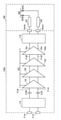
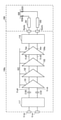
- FIG. 1 is a circuit diagram showing a configuration of a driver circuit according to a first embodiment of the present invention.
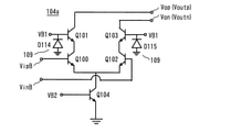
- FIG. 2 is a circuit diagram showing a configuration of an output circuit of the driver circuit according to the first embodiment of the present invention.
- 3A-3B are circuit diagrams illustrating the function of the ESD protection circuit of the driver circuit according to the first embodiment of the present invention.
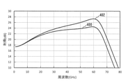
- FIG. 4 is a diagram showing a simulation result of the transmission characteristics of the conventional driver circuit and the driver circuit according to the first embodiment of the present invention.
- FIG. 5 is a diagram showing a simulation result of transmission characteristics of a configuration in which a conventional ESD protection circuit on the output side is used instead of the ESD protection circuit on the output side in the driver circuit according to the first embodiment of the present invention.
- FIG. 1 is a circuit diagram showing a configuration of a driver circuit according to a first embodiment of the present invention.
- FIG. 2 is a circuit diagram showing a configuration of an output circuit of the driver circuit according to the first embodiment of the present invention.
- FIG. 6 is a diagram showing a simulation result of transmission characteristics of a configuration in which a conventional ESD protection circuit on the input side is used instead of the ESD protection circuit on the input side in the driver circuit according to the first embodiment of the present invention.
- FIG. 7 is a circuit diagram showing a configuration of a driver circuit according to a second embodiment of the present invention.
- FIG. 8 is a circuit diagram showing a configuration of an ESD protection circuit on the output side of the driver circuit according to the second embodiment of the present invention.
- FIG. 9 is a circuit diagram showing a configuration of a driver circuit according to a third embodiment of the present invention.
- FIG. 10 is a circuit diagram showing a configuration of an ESD protection circuit on the input side of the driver circuit according to the third embodiment of the present invention.
- FIG. 11 is a circuit diagram showing a configuration of a driver circuit according to a fourth embodiment of the present invention.
- FIG. 12 is a circuit diagram showing a configuration of an ESD protection circuit on the input side of the driver circuit according to the fourth embodiment of the present invention.
- FIG. 13 is a circuit diagram showing a configuration of a driver circuit according to a fifth embodiment of the present invention.
- FIG. 14 is a circuit diagram showing a configuration of an ESD protection circuit on the input side of the driver circuit according to the fifth embodiment of the present invention.
- FIG. 15 is a circuit diagram showing a configuration of a driver circuit according to a sixth embodiment of the present invention.
- FIG. 16 is a circuit diagram showing a configuration of an ESD protection circuit on the input side of the driver circuit according to the sixth embodiment of the present invention.
- FIG. 17 is a circuit diagram showing the configuration of a conventional driver circuit.
- FIG. 18 is a circuit diagram showing a configuration of an output circuit of a conventional driver circuit.
- FIG. 1 is a circuit diagram showing a configuration of a driver circuit according to a first embodiment of the present invention.
- the driver circuit 100a of this embodiment adjusts the gain so that the amplitude of the input buffer 101 to which the differential signal for driving the MZM 200 is input and the differential signal output from the input buffer 101 are constant is constant.
- a pre-amplifier 103 that amplifies the differential signal output from the GCA 102, an open collector type output circuit 104a that drives the MZM200 in response to the differential signal output from the pre-amplifier 103, and a driver circuit at one end.
- the DC cut capacitor C100 connected to the input signal terminal Vinp on the positive phase side of 100a and the other end connected to the non-inverting input terminal VipA of the input buffer 101, and the input signal terminal Vinn on the opposite phase side of the driver circuit 100a at one end.
- the DC cut capacitor C101 the other end of which is connected to the inverting input terminal VinA of the input buffer 101, and the two input termination resistors R100 and R101 connected in series between the input signal terminals Vinp and Vinn, and the input termination. It is composed of an ESD protection circuit 107 connected to the connection points of the resistors R100 and R101 and an ESD protection circuit 108 connected to the output signal terminals Voutp and Voutn.
- the respective resistance values of the input terminating resistors R100 and R101 are 50 ⁇ .
- the ESD protection circuit 107 has a diode D110 in which the anode is connected to the connection points of the input terminating resistors R100 and R101 and the cathode is connected to the power supply voltage VCS, and the anode is connected to the ground and the cathode is the input terminating resistors R100 and R101. It is composed of a diode D111 connected to a connection point.
- the anode is connected to the output signal terminal Voutp on the positive phase side of the driver circuit 100a, the cathode is connected to the power supply voltage VCC, and the anode is the diode D112, and the anode is the output signal terminal on the opposite phase side of the driver circuit 100a. It is composed of a diode D113 connected to Voutn and having a cathode connected to a power supply voltage VCS.
- FIG. 2 is a circuit diagram showing the configuration of the output circuit 104a of the driver circuit 100a.
- the base terminal is connected to the input transistor Q100 connected to the non-inverting input terminal VipB of the output circuit 104a, the base terminal is connected to the bias voltage VB1, and the collector terminal is connected to the non-inverting output terminal Vop of the output circuit 104a.
- the output transistor Q101 whose emitter terminal is connected to the collector terminal of the input transistor Q100, the input transistor Q102 whose base terminal is connected to the inverting input terminal VinB of the output circuit 104a, and the base terminal are connected to the bias voltage VB1.
- the collector terminal is connected to the inverting output terminal Von of the output circuit 104a, the emitter terminal is connected to the output transistor Q103 connected to the collector terminal of the input transistor Q102, the base terminal is connected to the bias voltage VB2, and the collector terminal is connected to the input transistor Q100,
- the current source transistor Q104 which is connected to the emitter terminal of Q102 and the emitter terminal is connected to the ground, the diode D114 whose anode is connected to the ground and the cathode is connected to the base terminal of the output transistor Q101, and the anode is connected to the ground.
- the cathode is composed of a diode D115 connected to the base terminal of the output transistor Q103.
- Diodes D114 and D115 constitute an ESD protection circuit 109.
- the power supply voltage VCS of the driver circuit 100a, the power supply voltage VDC of the MZM200, and the bias voltages VB1 and VB2 (VCC ⁇ VB1> VB2) are positive voltages.
- the ESD protection circuit 107 is connected to the midpoint of the input terminating resistors R100 and R101 as shown in FIG.
- a positive voltage higher than the power supply voltage VCS is applied to the input signal terminal Vimp
- a current flows from the input signal terminal Vimp to the power supply voltage VCS side via the input terminating resistor R100 and the diode D110.
- a positive voltage higher than the power supply voltage VCS is applied to the input signal terminal Vinn
- a current flows from the input signal terminal Vinn to the power supply voltage VCC side via the input terminating resistor R101 and the diode D110. ..
- the differential input signal terminals Vimp and Vinn Since the influence of the parasitic capacitance added to the conventional driver circuit is weaker than that of the conventional driver circuit, it is possible to realize a wider frequency characteristic than the conventional one.
- the ESD protection circuit 108 is connected to the differential output signal terminals Voutp and Voutn, and the ESD protection circuit 109 is connected to the base terminals of the output transistors Q101 and Q103 of the output circuit 104a.
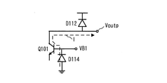
- FIG. 3A is a diagram showing the output transistor Q101 of FIG. 3A as an equivalent circuit including diodes D1010 and D1011.
- the parasitic capacitance of the diode D114 does not affect the output signal terminal Voutp (collector terminal of the output transistor Q101).
- the parasitic capacitance of the diode D115 does not affect the output signal terminal Voutn (collector terminal of the output transistor Q103). Therefore, according to the driver circuit 100a of this embodiment, it is possible to realize a frequency characteristic having a wider band than the conventional one.
- the output impedance of the output circuit 104a can be increased and oscillation is suppressed. There is also a synergistic effect of being able to do it.
- FIG. 4 shows the simulation results of the transmission characteristics of the conventional driver circuit 100 shown in FIG. 17 and the driver circuit 100a of this embodiment.
- 400 in FIG. 4 shows the transmission characteristics of the conventional driver circuit 100
- 401 shows the transmission characteristics of the driver circuit 100a of this embodiment.
- the ESD protection circuit 107 and the ESD protection circuits 108 and 109 are provided at the same time. However, only the ESD protection circuit 107 may be provided or only the ESD protection circuits 108 and 109 are provided. You may do so.
- FIG. 5 shows the simulation results of the transmission characteristics of the configuration in which the conventional ESD protection circuit 106 is used instead of the ESD protection circuits 108 and 109 in the driver circuit 100a of this embodiment. Similar to FIG. 4, 400 shows the transmission characteristics of the conventional driver circuit 100, and 402 shows the transmission characteristics of the configuration in which the ESD protection circuit 106 is used instead of the ESD protection circuits 108 and 109. According to FIG. 5, it can be seen that a wide band can be realized even when only the ESD protection circuit 107 is provided.
- FIG. 6 shows the simulation result of the transmission characteristic of the configuration in which the conventional ESD protection circuit 105 is used instead of the ESD protection circuit 107 in the driver circuit 100a of this embodiment. Similar to FIG. 4, 400 shows the transmission characteristics of the conventional driver circuit 100, and 403 shows the transmission characteristics of the configuration in which the ESD protection circuit 105 is used instead of the ESD protection circuit 107. According to FIG. 6, it can be seen that a wide band can be realized even when only the ESD protection circuits 108 and 109 are provided.
- FIG. 7 is a circuit diagram showing a configuration of a driver circuit according to a second embodiment of the present invention.
- the driver circuit 100b of this embodiment includes an input buffer 101, a GCA 102, a pre-amplifier 103, an output circuit 104a, DC cut capacitors C100 and C101, input termination resistors R100 and R101, and an ESD protection circuit 107. It is composed of an ESD protection circuit 110 connected between the output circuit 104a and the differential output signal terminals Voutp and Voutn of the driver circuit 100b.
- FIG. 8 is a circuit diagram showing the configuration of the ESD protection circuit 110.
- the ESD protection circuit 110 has a transmission line 111 whose input end is connected to the non-inverting output terminal Vop of the output circuit 104a and whose output end is connected to the output signal terminal Voutp on the positive phase side of the driver circuit 100b, and the input end is an output.
- a transmission line 112 connected to the inverting output terminal Von of the circuit 104a, the output end connected to the output signal terminal Voutn on the opposite phase side of the driver circuit 100b, and the transmission line 111 are arranged along the transmission line 111, and the anode is connected to the transmission line 111.
- the transmission line 111 has a configuration in which a plurality of transmission lines 1110, 1111, 1112 are connected in series.
- the characteristic impedance is different between the transmission line 1111 between the diodes D116 and the transmission line 1110 on the input side. The reason is that in the case of the transmission line 1110, it is necessary for the transmission line 1110 to absorb the influence of the parasitic capacitance of the output circuit 104a or the like in the previous stage.
- the transmission line 1111 and the transmission line 1112 have different characteristic impedances. The reason is that in the case of the transmission line 1112, it is necessary for the transmission line 1112 to absorb the influence of the parasitic capacitance of the MZM200 or the like in the subsequent stage.
- the transmission line 112 has a configuration in which a plurality of transmission lines 1120, 1121, 1122 are connected in series.
- the characteristic impedance of the transmission line 1121 between the diodes D117 and the transmission line 1120 on the input side are different. The reason is that in the case of the transmission line 1120, it is necessary for the transmission line 1120 to absorb the influence of the parasitic capacitance of the output circuit 104a or the like in the previous stage.
- the transmission line 1121 and the transmission line 1122 have different characteristic impedances. The reason is that in the case of the transmission line 1122, it is necessary for the transmission line 1122 to absorb the influence of the parasitic capacitance of the MZM200 or the like in the subsequent stage.
- diodes D112 and D113 having a large size (current capacity) were used in order to satisfy the allowable withstand voltage against static electricity.
- the diode D112 is divided into a diode D116 having a small size so that the total size (total current capacity) of the diode D116 becomes equal to the size of the diode D112.
- the diode D113 is divided into small size diodes D117 so that the total size of the diodes D117 is equal to the size of the diode D113.
- the driver It is possible to prevent multiple reflection of the signal at the connection point between the circuit 100b and the MZM200.
- the cutoff frequency of the pseudo transmission line is basically regulated by the parasitic capacitance of the diode connected to the transmission line per unit length, the smaller the diode size and the larger the number of diodes, the more the driver circuit.
- the bandwidth of 100b can be increased. That is, if the number of each of the diodes D116 and D117 is N (N is an integer of 2 or more), the size of each of the diodes D116 and D117 is set to 1 / N of the size of the diodes D112 and D113.
- the loss of the transmission lines 111 and 112 is large, it becomes difficult to widen the band, so it is desirable that the loss of the transmission lines 111 and 112 is small.
- the influence of the diodes D116 and D117 connected to the power supply voltage VCS is reduced by the transmission lines 111 and 112, and the influence of the diodes D114 and D115 connected to the ground is affected by the output transistor of the output circuit 104a.
- the combination with the configuration reduced by Q101 and Q103 has a synergistic effect on widening the bandwidth of the driver circuit 100b. The reason is that, as described above, the parasitic capacitance of the diode connected to the transmission line per unit length can be reduced and the cutoff frequency can be increased.
- the configuration is described in which the ESD protection circuit 107 and the ESD protection circuits 109 and 110 are provided at the same time, but only the ESD protection circuits 109 and 110 may be provided.
- FIG. 9 is a circuit diagram showing a configuration of a driver circuit according to a third embodiment of the present invention.
- the driver circuit 100c of this embodiment includes an input buffer 101, a GCA 102, a pre-amplifier 103, an output circuit 104a, DC cut capacitors C100 and C101, an ESD protection circuit 110, and a differential input signal of the driver circuit 100c. It is composed of an ESD protection circuit 113 connected to terminals Vinp and Vinn.
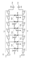
- FIG. 10 is a circuit diagram showing the configuration of the ESD protection circuit 113.
- the ESD protection circuit 113 has a transmission line 114 whose input end is connected to the input signal terminal Diode on the positive phase side of the driver circuit 100c and whose output end is connected to one end of the DC cut capacitor C100, and whose input end is the driver circuit 100c.
- a transmission line 115 connected to the input signal terminal Vinn on the opposite phase side and having an output end connected to one end of the DC cut capacitor C101, and a plurality of transmission lines 115 arranged along the transmission line 114 and having one end connected to the transmission line 114.
- the transmission line 114 has a configuration in which a plurality of transmission lines 1140, 1141, 1142 are connected in series.
- the characteristic impedance of the transmission line 1141 between the input terminating resistors R102 and the transmission line 1140 on the input side is different. The reason is that in the case of the transmission line 1140, it is necessary for the transmission line 1140 to absorb the influence of the parasitic capacitance of the circuit in the previous stage and the like.
- the transmission line 1141 and the transmission line 1142 have different characteristic impedances. The reason is that in the case of the transmission line 1142, it is necessary for the transmission line 1142 to absorb the influence of the capacitance of the DC cut capacitor C100 or the like in the subsequent stage.
- the transmission line 115 has a configuration in which a plurality of transmission lines 1150, 1151, 1152 are connected in series.
- the characteristic impedance is different between the transmission line 1151 between the input terminating resistor R103 and the transmission line 1150 on the input side. The reason is that in the case of the transmission line 1150, it is necessary for the transmission line 1150 to absorb the influence of the parasitic capacitance of the circuit in the previous stage and the like.
- the transmission line 1151 and the transmission line 1152 have different characteristic impedances. The reason is that in the case of the transmission line 1152, it is necessary for the transmission line 1152 to absorb the influence of the capacitance of the DC cut capacitor C101 or the like in the subsequent stage.
- the influence of band deterioration due to the diode of the ESD protection circuit connected to the differential input signal terminals Vimp and Vinn is further reduced.
- the diode D110 of the ESD protection circuit 107 of the first and second embodiments is divided into a diode D118 having a small size, and the total size (total current capacity) of the diode D118 is equal to the size of the diode D110.
- the diode D111 of the ESD protection circuit 107 is divided into a diode D119 having a small size so that the total size of the diodes D119 becomes equal to the size of the diode D111.
- the characteristic impedance of the pseudo transmission line composed of the transmission line 114, the diode D118 and the input termination resistor R102, and the characteristic impedance of the pseudo transmission line composed of the transmission line 115, the diode D119 and the input termination resistor R103 are set to 50 ⁇ . do.
- the size of the diodes D118 and D119 is set to 1 / N of the sizes of the diodes D110 and D111. Further, the resistance values of the N input terminating resistors R102 and the N input terminating resistors R103 are set to N ⁇ 50 ⁇ .
- the influence of band deterioration due to the diode of the ESD protection circuit on the input side can be further reduced, and the bandwidth is further widened as compared with the first and second embodiments. It is possible to make it.
- FIG. 9 shows an example in which the ESD protection circuit 113 of this embodiment is applied to the second embodiment
- the ESD protection circuit 113 may be applied to the first embodiment. That is, in FIG. 9, the ESD protection circuit 108 may be provided instead of the ESD protection circuit 110.
- FIG. 11 is a circuit diagram showing a configuration of a driver circuit according to a fourth embodiment of the present invention.
- the driver circuit 100d of this embodiment includes an input buffer 101, a GCA 102, a pre-amplifier 103, an output circuit 104a, DC cut capacitors C100 and C101, an ESD protection circuit 110, and a differential input signal of the driver circuit 100d. It is composed of an ESD protection circuit 116 connected to terminals Vinp and Vinn.
- FIG. 12 is a circuit diagram showing the configuration of the ESD protection circuit 116.
- the ESD protection circuit 116 has a transmission line 114 whose input end is connected to the input signal terminal Vimp on the positive phase side of the driver circuit 100d and whose output end is connected to one end of the DC cut capacitor C100, and whose input end is the driver circuit 100d.
- a transmission line 115 connected to the input signal terminal Vinn on the opposite phase side and having an output end connected to one end of the DC cut capacitor C101, and a plurality of transmission lines 115 arranged along the transmission line 114 and having one end connected to the transmission line 114.
- a plurality of diodes provided for every other set of the plurality of sets of the input terminating resistors R102 and R103, the anode is connected to the connection point of the input terminating resistors R102 and R103, and the cathode is connected to the power supply voltage VCS.
- the influence of band deterioration due to the diode of the ESD protection circuit connected to the differential input signal terminals Vimp and Vinn is further reduced.
- the diode D110 of the ESD protection circuit 107 of the first and second embodiments is divided into a diode D120 having a small size, and the total size (total current capacity) of the diode D120 is equal to the size of the diode D110.
- the diode D111 of the ESD protection circuit 107 is divided into a diode D121 having a small size so that the total size of the diodes D121 becomes equal to the size of the diode D111.
- the unit cell in which the diode D120 is connected to the midpoint of the input terminating resistors R102 and R103 and the unit cell in which the diode D121 is connected to the midpoint of the input terminating resistors R102 and R103 are alternately arranged. do.
- the characteristic impedance of the pseudo transmission line composed of the transmission line 114, the diode D120 and the input termination resistor R102, and the characteristic impedance of the pseudo transmission line composed of the transmission line 115, the diode D121 and the input termination resistor R103 are obtained. It is set to 50 ⁇ .
- the size of each of the diodes D120 and D121 is set to 2 / N of the size of the diodes D110 and D111. Further, the resistance values of the N input terminating resistors R102 and the N input terminating resistors R103 are set to N ⁇ 50 ⁇ .
- the parasitic capacitance of the diode connected to the transmission line per unit length can be reduced and the cutoff frequency can be increased. Further widening of the band is possible as compared with the examples.
- FIG. 11 shows an example in which the ESD protection circuit 116 of this embodiment is applied to the second embodiment
- the ESD protection circuit 116 may be applied to the first embodiment. That is, in FIG. 11, the ESD protection circuit 108 may be provided instead of the ESD protection circuit 110.
- FIG. 13 is a circuit diagram showing a configuration of a driver circuit according to a fifth embodiment of the present invention.
- the driver circuit 100e of this embodiment includes an input buffer 101, a GCA 102, a pre-amplifier 103, an output circuit 104a, DC cut capacitors C100 and C101, an ESD protection circuit 110, and a differential input signal of the driver circuit 100e. It is composed of an ESD protection circuit 117 connected to terminals Vinp and Vinn.
- FIG. 14 is a circuit diagram showing the configuration of the ESD protection circuit 117.
- the ESD protection circuit 117 has a transmission line 114 whose input end is connected to the input signal terminal Diode on the positive phase side of the driver circuit 100e and whose output end is connected to one end of the DC cut capacitor C100, and whose input end is the driver circuit 100e.
- the transmission line 115 which is connected to the input signal terminal VIN on the opposite phase side and whose output end is connected to one end of the DC cut capacitor C101, is connected in series between the output end of the transmission line 114 and the output end of the transmission line 115.
- Two input termination resistors R104 and R105, and a plurality of diodes D122 arranged along the transmission line 114, the anode connected to the transmission line 114, and the cathode connected to the power supply voltage VCS, and each diode D122 are provided.
- the anode is connected to the ground
- the cathode is located along the transmission line 115 with a plurality of diodes D123 connected to the diode of the diode D122
- the anode is connected to the transmission line 115
- the cathode is connected to the power supply voltage VCS.
- It is composed of a plurality of diodes D124 provided, and a plurality of diodes D125 provided for each diode D124, the anode is connected to the ground, and the cathode is connected to the anode of the diode D124.
- the diode D110 of the ESD protection circuit 107 of the first and second embodiments is divided into small size diodes D122 and D124, and the total size of the diode D122 and the total size of the diode D124 are each of the diode D110. Make it equal to the size.
- the diode D111 of the ESD protection circuit 107 is divided into small size diodes D123 and D125 so that the total size of the diode D123 and the total size of the diode D125 are each equal to the size of the diode D111.
- the characteristic impedance of the pseudo transmission line composed of the transmission line 114 and the diodes D122 and D123, and the characteristic impedance of the pseudo transmission line composed of the transmission line 115 and the diodes D124 and D125 are set to 50 ⁇ .
- the size of the diodes D122 to D125 is set to 1 / N of the sizes of the diodes D110 and D111. Further, the resistance values of the input terminating resistors R104 and R105 are set to 50 ⁇ .
- FIG. 13 shows an example in which the ESD protection circuit 117 of this embodiment is applied to the second embodiment
- the ESD protection circuit 117 may be applied to the first embodiment. That is, in FIG. 13, the ESD protection circuit 108 may be provided instead of the ESD protection circuit 110.
- FIG. 15 is a circuit diagram showing a configuration of a driver circuit according to a sixth embodiment of the present invention.
- the driver circuit 100f of this embodiment includes an input buffer 101, a GCA 102, a pre-amplifier 103, an output circuit 104a, DC cut capacitors C100 and C101, an ESD protection circuit 110, and a differential input signal of the driver circuit 100f. It is composed of an ESD protection circuit 118 connected to terminals Vinp and Vinn.
- FIG. 16 is a circuit diagram showing the configuration of the ESD protection circuit 118.
- the ESD protection circuit 118 has a transmission line 114 whose input end is connected to the input signal terminal Vimp on the positive phase side of the driver circuit 100f and whose output end is connected to one end of the DC cut capacitor C100, and whose input end is the driver circuit 100f.
- a transmission line 115 connected to the input signal terminal Vinn on the opposite phase side and having an output end connected to one end of the DC cut capacitor C101, and connected in series between the output end of the transmission line 114 and the output end of the transmission line 115.
- the influence of band deterioration due to the diode of the ESD protection circuit connected to the differential input signal terminals Vimp and Vinn is further reduced.
- the diode D110 of the ESD protection circuit 107 of the first and second embodiments is divided into small size diodes D126 and D128, and the total size of the diode D126 and the total size of the diode D128 are each of the diode D110. Make it equal to the size.
- the diode D111 of the ESD protection circuit 107 is divided into small size diodes D127 and D129 so that the total size of the diode D127 and the total size of the diode D129 are each equal to the size of the diode D111.
- the diodes D126 and D127 are alternately arranged so that the diode D126 and the diode D127 are connected to different points of the transmission line 114.
- the diodes D128 and D129 are alternately arranged so that the diode D128 and the diode D129 are connected to different points of the transmission line 115.
- the characteristic impedance of the pseudo transmission line composed of the transmission line 114 and the diodes D126 and D127, and the characteristic impedance of the pseudo transmission line composed of the transmission line 115 and the diodes D128 and D129 are set to 50 ⁇ .
- the size of the diodes D126 to D129 is the size of the diodes D110 and D111, respectively.
- the resistance values of the input terminating resistors R104 and R105 are set to 50 ⁇ .
- the parasitic capacitance of the diode connected to the transmission line per unit length can be reduced and the cutoff frequency can be increased. Further widening of the band is possible as compared with the examples.
- FIG. 15 shows an example in which the ESD protection circuit 118 of this embodiment is applied to the second embodiment
- the ESD protection circuit 118 may be applied to the first embodiment. That is, in FIG. 15, the ESD protection circuit 108 may be provided instead of the ESD protection circuit 110.
- the present invention can be applied to a driver circuit for driving an optical modulator.
- 100a-100f ... Driver circuit 101 ... Input buffer, 102 ... Gain control amplifier, 103 ... Pre-amplifier, 104a ... Output circuit, 107-110, 113, 116-118 ... ESD protection circuit, 111, 112, 114, 115 , 1110, 1111, 1112, 1120, 1121, 1122, 1140, 1141, 1142, 1150, 1151, 1152 ... Transmission line, Q100 to Q104 ... Transistor, D110 to D129 ... Diode, C100, C101 ... DC cut capacitor, R100 to R105 ... Input terminating resistor.
Landscapes
- Engineering & Computer Science (AREA)
- Power Engineering (AREA)
- Optical Modulation, Optical Deflection, Nonlinear Optics, Optical Demodulation, Optical Logic Elements (AREA)
- Amplifiers (AREA)
- Logic Circuits (AREA)
Abstract
Description
図18は出力回路104の構成を示す回路図である。出力回路104は、トランジスタQ100~Q104から構成される。
一方、ドライバ回路100の入力信号端子Vinp,Vinnに電源電圧VCCよりも高い電圧が印加された場合には、入力信号端子Vinp,VinnからダイオードD100,D102を経由して電源電圧VCC側に電流が流れることにより、ドライバ回路100のトランジスタが保護される。また、入力信号端子Vinp,Vinnにグラウンドよりも低い電圧が印加された場合には、グラウンドからダイオードD101,D103を経由して入力信号端子Vinp,Vinn側に電流が流れることにより、ドライバ回路100のトランジスタが保護される。
以下、本発明の実施例について図面を参照して説明する。図1は本発明の第1の実施例に係るドライバ回路の構成を示す回路図である。本実施例のドライバ回路100aは、MZM200の駆動のための差動信号が入力される入力バッファ101と、入力バッファ101から出力された差動信号の振幅が一定になるように利得を調整するGCA102と、GCA102から出力された差動信号を増幅する前置増幅器103と、前置増幅器103から出力された差動信号に応じてMZM200を駆動するオープンコレクタ型の出力回路104aと、一端がドライバ回路100aの正相側の入力信号端子Vinpに接続され、他端が入力バッファ101の非反転入力端子VipAに接続されたDCカットキャパシタC100と、一端がドライバ回路100aの逆相側の入力信号端子Vinnに接続され、他端が入力バッファ101の反転入力端子VinAに接続されたDCカットキャパシタC101と、入力信号端子Vinp,Vinn間に直列に接続された2つの入力終端抵抗R100,R101と、入力終端抵抗R100,R101の接続点に接続されたESD保護回路107と、出力信号端子Voutp,Voutnに接続されたESD保護回路108とから構成される。入力終端抵抗R100,R101のそれぞれの抵抗値は50Ωである。
入力信号端子Vinpに電源電圧VCCよりも高い正の電圧が印加された場合には、入力信号端子Vinpから入力終端抵抗R100とダイオードD110とを経由して電源電圧VCC側に電流が流れる。同様に、入力信号端子Vinnに電源電圧VCCよりも高い正の電圧が印加された場合には、入力信号端子Vinnから入力終端抵抗R101とダイオードD110とを経由して電源電圧VCC側に電流が流れる。
次に、本実施例の第2の実施例について説明する。図7は本発明の第2の実施例に係るドライバ回路の構成を示す回路図である。本実施例のドライバ回路100bは、入力バッファ101と、GCA102と、前置増幅器103と、出力回路104aと、DCカットキャパシタC100,C101と、入力終端抵抗R100,R101と、ESD保護回路107と、出力回路104aとドライバ回路100bの差動出力信号端子Voutp,Voutnとの間に接続されたESD保護回路110とから構成される。
図8はESD保護回路110の構成を示す回路図である。ESD保護回路110は、入力端が出力回路104aの非反転出力端子Vopに接続され、出力端がドライバ回路100bの正相側の出力信号端子Voutpに接続された伝送線路111と、入力端が出力回路104aの反転出力端子Vonに接続され、出力端がドライバ回路100bの逆相側の出力信号端子Voutnに接続された伝送線路112と、伝送線路111に沿って配置され、アノードが伝送線路111に接続され、カソードが電源電圧VCCに接続された複数のダイオードD116と、伝送線路112に沿って配置され、アノードが伝送線路112に接続され、カソードが電源電圧VCCに接続された複数のダイオードD117とから構成される。
ただし、伝送線路111,112の損失が大きい場合は広帯域化が困難になるので、伝送線路111,112の損失は小さい方が望ましい。
なお、グラウンドに接続されるダイオードをESD保護回路110と同様に疑似伝送線路に組み込んだ場合には、寄生容量が大きくなり、カットオフ周波数が低くなる。
次に、本発明の第3の実施例について説明する。図9は本発明の第3の実施例に係るドライバ回路の構成を示す回路図である。本実施例のドライバ回路100cは、入力バッファ101と、GCA102と、前置増幅器103と、出力回路104aと、DCカットキャパシタC100,C101と、ESD保護回路110と、ドライバ回路100cの差動入力信号端子Vinp,Vinnに接続されたESD保護回路113とから構成される。
図10はESD保護回路113の構成を示す回路図である。ESD保護回路113は、入力端がドライバ回路100cの正相側の入力信号端子Vinpに接続され、出力端がDCカットキャパシタC100の一端に接続された伝送線路114と、入力端がドライバ回路100cの逆相側の入力信号端子Vinnに接続され、出力端がDCカットキャパシタC101の一端に接続された伝送線路115と、伝送線路114に沿って配置され、一端が伝送線路114に接続された複数の入力終端抵抗R102と、伝送線路115に沿って配置され、一端が伝送線路115に接続され、他端が入力終端抵抗R102の他端に接続された複数の入力終端抵抗R103と、直列に接続された入力終端抵抗R102,R103の組毎に設けられ、アノードが入力終端抵抗R102,R103の接続点に接続され、カソードが電源電圧VCCに接続された複数のダイオードD118と、ダイオードD118毎に設けられ、アノードがグラウンドに接続され、カソードがダイオードD118のアノードに接続された複数のダイオードD119とから構成される。
また、N個の入力終端抵抗R102とN個の入力終端抵抗R103のそれぞれの抵抗値をN×50Ωとする。
次に、本発明の第4の実施例について説明する。図11は本発明の第4の実施例に係るドライバ回路の構成を示す回路図である。本実施例のドライバ回路100dは、入力バッファ101と、GCA102と、前置増幅器103と、出力回路104aと、DCカットキャパシタC100,C101と、ESD保護回路110と、ドライバ回路100dの差動入力信号端子Vinp,Vinnに接続されたESD保護回路116とから構成される。
図12はESD保護回路116の構成を示す回路図である。ESD保護回路116は、入力端がドライバ回路100dの正相側の入力信号端子Vinpに接続され、出力端がDCカットキャパシタC100の一端に接続された伝送線路114と、入力端がドライバ回路100dの逆相側の入力信号端子Vinnに接続され、出力端がDCカットキャパシタC101の一端に接続された伝送線路115と、伝送線路114に沿って配置され、一端が伝送線路114に接続された複数の入力終端抵抗R102と、伝送線路115に沿って配置され、一端が伝送線路115に接続され、他端が入力終端抵抗R102の他端に接続された複数の入力終端抵抗R103と、直列に接続された入力終端抵抗R102,R103の複数の組のうち1つおきの組毎に設けられ、アノードが入力終端抵抗R102,R103の接続点に接続され、カソードが電源電圧VCCに接続された複数のダイオードD120と、アノードがグラウンドに接続され、入力終端抵抗R102,R103の複数の組のうちダイオードD120が接続されていない入力終端抵抗R102,R103の接続点にカソードが接続された複数のダイオードD121とから構成される。
また、N個の入力終端抵抗R102とN個の入力終端抵抗R103のそれぞれの抵抗値をN×50Ωとする。
次に、本発明の第5の実施例について説明する。図13は本発明の第5の実施例に係るドライバ回路の構成を示す回路図である。本実施例のドライバ回路100eは、入力バッファ101と、GCA102と、前置増幅器103と、出力回路104aと、DCカットキャパシタC100,C101と、ESD保護回路110と、ドライバ回路100eの差動入力信号端子Vinp,Vinnに接続されたESD保護回路117とから構成される。
図14はESD保護回路117の構成を示す回路図である。ESD保護回路117は、入力端がドライバ回路100eの正相側の入力信号端子Vinpに接続され、出力端がDCカットキャパシタC100の一端に接続された伝送線路114と、入力端がドライバ回路100eの逆相側の入力信号端子Vinnに接続され、出力端がDCカットキャパシタC101の一端に接続された伝送線路115と、伝送線路114の出力端と伝送線路115の出力端との間に直列に接続された2つの入力終端抵抗R104,R105と、伝送線路114に沿って配置され、アノードが伝送線路114に接続され、カソードが電源電圧VCCに接続された複数のダイオードD122と、ダイオードD122毎に設けられ、アノードがグラウンドに接続され、カソードがダイオードD122のアノードに接続された複数のダイオードD123と、伝送線路115に沿って配置され、アノードが伝送線路115に接続され、カソードが電源電圧VCCに接続された複数のダイオードD124と、ダイオードD124毎に設けられ、アノードがグラウンドに接続され、カソードがダイオードD124のアノードに接続された複数のダイオードD125とから構成される。
また、入力終端抵抗R104,R105のそれぞれの抵抗値を50Ωとする。
次に、本発明の第6の実施例について説明する。図15は本発明の第6の実施例に係るドライバ回路の構成を示す回路図である。本実施例のドライバ回路100fは、入力バッファ101と、GCA102と、前置増幅器103と、出力回路104aと、DCカットキャパシタC100,C101と、ESD保護回路110と、ドライバ回路100fの差動入力信号端子Vinp,Vinnに接続されたESD保護回路118とから構成される。
図16はESD保護回路118の構成を示す回路図である。ESD保護回路118は、入力端がドライバ回路100fの正相側の入力信号端子Vinpに接続され、出力端がDCカットキャパシタC100の一端に接続された伝送線路114と、入力端がドライバ回路100fの逆相側の入力信号端子Vinnに接続され、出力端がDCカットキャパシタC101の一端に接続された伝送線路115と、伝送線路114の出力端と伝送線路115の出力端との間に直列に接続された2つの入力終端抵抗R104,R105と、伝送線路114に沿って配置され、アノードが伝送線路114に接続され、カソードが電源電圧VCCに接続された複数のダイオードD126と、伝送線路114に沿って配置され、アノードがグラウンドに接続され、カソードが伝送線路114に接続された複数のダイオードD127と、伝送線路115に沿って配置され、アノードが伝送線路115に接続され、カソードが電源電圧VCCに接続された複数のダイオードD128と、伝送線路115に沿って配置され、アノードがグラウンドに接続され、カソードが伝送線路115に接続された複数のダイオードD129とから構成される。
また、入力終端抵抗R104,R105のそれぞれの抵抗値を50Ωとする。
Claims (8)
- 一端がドライバ回路の正相側の第1の入力信号端子に接続された第1のキャパシタと、
一端がドライバ回路の逆相側の第2の入力信号端子に接続された第2のキャパシタと、
非反転入力端子が前記第1のキャパシタの他端に接続され、反転入力端子が前記第2のキャパシタの他端に接続された入力バッファと、
前記第1の入力信号端子と前記第2の入力信号端子との間に直列に接続された第1、第2の入力終端抵抗と、
前記第1、第2の入力終端抵抗の接続点に接続されたESD保護回路とを備え、
前記ESD保護回路は、
アノードが前記第1、第2の入力終端抵抗の接続点に接続され、カソードが電源電圧に接続された第1のダイオードと、
アノードがグラウンドに接続され、カソードが前記第1、第2の入力終端抵抗の接続点に接続された第2のダイオードとから構成されることを特徴とするドライバ回路。 - ドライバ回路の正相側の第1の入力信号端子と逆相側の第2の入力信号端子とに接続されたESD保護回路と、
一端が前記ESD保護回路に接続された第1、第2のキャパシタと、
非反転入力端子が前記第1のキャパシタの他端に接続され、反転入力端子が前記第2のキャパシタの他端に接続された入力バッファとを備え、
前記ESD保護回路は、
入力端が前記第1の入力信号端子に接続され、出力端が前記第1のキャパシタの一端に接続された第1の伝送線路と、
入力端が前記第2の入力信号端子に接続され、出力端が前記第2のキャパシタの一端に接続された第2の伝送線路と、
前記第1の伝送線路に沿って配置され、一端が前記第1の伝送線路に接続された複数の第1の入力終端抵抗と、
前記第2の伝送線路に沿って配置され、一端が前記第2の伝送線路に接続され、他端が前記第1の入力終端抵抗の他端に接続された複数の第2の入力終端抵抗と、
直列に接続された前記第1、第2の入力終端抵抗の組毎に設けられ、アノードが前記第1、第2の入力終端抵抗の接続点に接続され、カソードが電源電圧に接続された複数の第1のダイオードと、
前記第1のダイオード毎に設けられ、アノードがグラウンドに接続され、カソードが前記第1のダイオードのアノードに接続された複数の第2のダイオードとから構成されることを特徴とするドライバ回路。 - ドライバ回路の正相側の第1の入力信号端子と逆相側の第2の入力信号端子とに接続されたESD保護回路と、
一端が前記ESD保護回路に接続された第1、第2のキャパシタと、
非反転入力端子が前記第1のキャパシタの他端に接続され、反転入力端子が前記第2のキャパシタの他端に接続された入力バッファとを備え、
前記ESD保護回路は、
入力端が前記第1の入力信号端子に接続され、出力端が前記第1のキャパシタの一端に接続された第1の伝送線路と、
入力端が前記第2の入力信号端子に接続され、出力端が前記第2のキャパシタの一端に接続された第2の伝送線路と、
前記第1の伝送線路に沿って配置され、一端が前記第1の伝送線路に接続された複数の第1の入力終端抵抗と、
前記第2の伝送線路に沿って配置され、一端が前記第2の伝送線路に接続され、他端が前記第1の入力終端抵抗の他端に接続された複数の第2の入力終端抵抗と、
直列に接続された前記第1、第2の入力終端抵抗の複数の組のうち1つおきの組毎に設けられ、アノードが前記第1、第2の入力終端抵抗の接続点に接続され、カソードが電源電圧に接続された複数の第1のダイオードと、
アノードがグラウンドに接続され、前記第1、第2の入力終端抵抗の複数の組のうち前記第1のダイオードが接続されていない第1、第2の入力終端抵抗の接続点にカソードが接続された複数の第2のダイオードとから構成されることを特徴とするドライバ回路。 - ドライバ回路の正相側の第1の入力信号端子と逆相側の第2の入力信号端子とに接続されたESD保護回路と、
一端が前記ESD保護回路に接続された第1、第2のキャパシタと、
非反転入力端子が前記第1のキャパシタの他端に接続され、反転入力端子が前記第2のキャパシタの他端に接続された入力バッファとを備え、
前記ESD保護回路は、
入力端が前記第1の入力信号端子に接続され、出力端が前記第1のキャパシタの一端に接続された第1の伝送線路と、
入力端が前記第2の入力信号端子に接続され、出力端が前記第2のキャパシタの一端に接続された第2の伝送線路と、
前記第1の伝送線路の出力端と前記第2の伝送線路の出力端との間に直列に接続された第1、第2の入力終端抵抗と、
前記第1の伝送線路に沿って配置され、アノードが前記第1の伝送線路に接続され、カソードが電源電圧に接続された複数の第1のダイオードと、
前記第1のダイオード毎に設けられ、アノードがグラウンドに接続され、カソードが前記第1のダイオードのアノードに接続された複数の第2のダイオードと、
前記第2の伝送線路に沿って配置され、アノードが前記第2の伝送線路に接続され、カソードが前記電源電圧に接続された複数の第3のダイオードと、
前記第3のダイオード毎に設けられ、アノードがグラウンドに接続され、カソードが前記第3のダイオードのアノードに接続された複数の第4のダイオードとから構成されることを特徴とするドライバ回路。 - ドライバ回路の正相側の第1の入力信号端子と逆相側の第2の入力信号端子とに接続されたESD保護回路と、
一端が前記ESD保護回路に接続された第1、第2のキャパシタと、
非反転入力端子が前記第1のキャパシタの他端に接続され、反転入力端子が前記第2のキャパシタの他端に接続された入力バッファとを備え、
前記ESD保護回路は、
入力端が前記第1の入力信号端子に接続され、出力端が前記第1のキャパシタの一端に接続された第1の伝送線路と、
入力端が前記第2の入力信号端子に接続され、出力端が前記第2のキャパシタの一端に接続された第2の伝送線路と、
前記第1の伝送線路の出力端と前記第2の伝送線路の出力端との間に直列に接続された第1、第2の入力終端抵抗と、
前記第1の伝送線路に沿って配置され、アノードが前記第1の伝送線路に接続され、カソードが電源電圧に接続された複数の第1のダイオードと、
前記第1のダイオード毎に設けられ、アノードがグラウンドに接続され、カソードが前記第1の伝送線路に接続された複数の第2のダイオードと、
前記第2の伝送線路に沿って配置され、アノードが前記第2の伝送線路に接続され、カソードが前記電源電圧に接続された複数の第3のダイオードと、
前記第3のダイオード毎に設けられ、アノードがグラウンドに接続され、カソードが前記第2の伝送線路に接続された複数の第4のダイオードとから構成され、
前記第1のダイオードと前記第2のダイオードとは、前記第1の伝送線路の異なる点に接続されるように交互に配置され、
前記第3のダイオードと前記第4のダイオードとは、前記第2の伝送線路の異なる点に接続されるように交互に配置されることを特徴とするドライバ回路。 - 非反転出力端子がドライバ回路の正相側の第1の出力信号端子に接続され、反転出力端子がドライバ回路の逆相側の第2の出力信号端子に接続された出力回路と、
前記第1、第2の出力信号端子に接続された第1のESD保護回路とを備え、
前記第1のESD保護回路は、
アノードが前記第1の出力信号端子に接続され、カソードが電源電圧に接続された第1のダイオードと、
アノードが前記第2の出力信号端子に接続され、カソードが前記電源電圧に接続された第2のダイオードとから構成され、
前記出力回路は、
ベース端子に光変調器の駆動のための差動信号が入力される第1、第2のトランジスタと、
コレクタ端子が前記第1の出力信号端子に接続され、エミッタ端子が前記第1のトランジスタのコレクタ端子に接続された第3のトランジスタと、
コレクタ端子が前記第2の出力信号端子に接続され、エミッタ端子が前記第2のトランジスタのコレクタ端子に接続された第4のトランジスタと、
前記第3、第4のトランジスタのベース端子に接続された第2のESD保護回路とから構成され、
前記第2のESD保護回路は、
アノードがグラウンドに接続され、カソードが前記第3のトランジスタのベース端子に接続された第3のダイオードと、
アノードがグラウンドに接続され、カソードが前記第4のトランジスタのベース端子に接続された第4のダイオードとから構成されることを特徴とするドライバ回路。 - 非反転出力端子がドライバ回路の正相側の第1の出力信号端子に接続され、反転出力端子がドライバ回路の逆相側の第2の出力信号端子に接続された出力回路と、
前記出力回路と前記第1、第2の出力信号端子との間に接続された第1のESD保護回路とを備え、
前記第1のESD保護回路は、
入力端が前記出力回路の非反転出力端子に接続され、出力端が前記第1の出力信号端子に接続された第1の伝送線路と、
入力端が前記出力回路の反転出力端子に接続され、出力端が前記第2の出力信号端子に接続された第2の伝送線路と、
前記第1の伝送線路に沿って配置され、アノードが前記第1の伝送線路に接続され、カソードが電源電圧に接続された複数の第1のダイオードと、
前記第2の伝送線路に沿って配置され、アノードが前記第2の伝送線路に接続され、カソードが前記電源電圧に接続された複数の第2のダイオードとから構成され、
前記出力回路は、
ベース端子に光変調器の駆動のための差動信号が入力される第1、第2のトランジスタと、
コレクタ端子が前記第1の出力信号端子に接続され、エミッタ端子が前記第1のトランジスタのコレクタ端子に接続された第3のトランジスタと、
コレクタ端子が前記第2の出力信号端子に接続され、エミッタ端子が前記第2のトランジスタのコレクタ端子に接続された第4のトランジスタと、
前記第3、第4のトランジスタのベース端子に接続された第2のESD保護回路とから構成され、
前記第2のESD保護回路は、
アノードがグラウンドに接続され、カソードが前記第3のトランジスタのベース端子に接続された第3のダイオードと、
アノードがグラウンドに接続され、カソードが前記第4のトランジスタのベース端子に接続された第4のダイオードとから構成されることを特徴とするドライバ回路。 - 請求項6または7記載のドライバ回路において、
前記出力回路は、
ベース端子が出力回路の非反転入力端子に接続された前記第1のトランジスタと、
ベース端子が出力回路の反転入力端子に接続された前記第2のトランジスタと、
ベース端子が第1のバイアス電圧に接続され、コレクタ端子が前記第1の出力信号端子に接続され、エミッタ端子が前記第1のトランジスタのコレクタ端子に接続された前記第3のトランジスタと、
ベース端子が前記第1のバイアス電圧に接続され、コレクタ端子が前記第2の出力信号端子に接続され、エミッタ端子が前記第2のトランジスタのコレクタ端子に接続された前記第4のトランジスタと、
ベース端子が第2のバイアス電圧に接続され、コレクタ端子が前記第1、第2のトランジスタのエミッタ端子に接続され、エミッタ端子がグラウンドに接続された第5のトランジスタと、
前記第2のESD保護回路とから構成されることを特徴とするドライバ回路。
Priority Applications (3)
| Application Number | Priority Date | Filing Date | Title |
|---|---|---|---|
| PCT/JP2020/028253 WO2022018823A1 (ja) | 2020-07-21 | 2020-07-21 | ドライバ回路 |
| JP2022538526A JP7420258B2 (ja) | 2020-07-21 | 2020-07-21 | ドライバ回路 |
| US18/005,938 US12278625B2 (en) | 2020-07-21 | 2020-07-21 | Driver circuit |
Applications Claiming Priority (1)
| Application Number | Priority Date | Filing Date | Title |
|---|---|---|---|
| PCT/JP2020/028253 WO2022018823A1 (ja) | 2020-07-21 | 2020-07-21 | ドライバ回路 |
Publications (1)
| Publication Number | Publication Date |
|---|---|
| WO2022018823A1 true WO2022018823A1 (ja) | 2022-01-27 |
Family
ID=79729346
Family Applications (1)
| Application Number | Title | Priority Date | Filing Date |
|---|---|---|---|
| PCT/JP2020/028253 Ceased WO2022018823A1 (ja) | 2020-07-21 | 2020-07-21 | ドライバ回路 |
Country Status (3)
| Country | Link |
|---|---|
| US (1) | US12278625B2 (ja) |
| JP (1) | JP7420258B2 (ja) |
| WO (1) | WO2022018823A1 (ja) |
Families Citing this family (1)
| Publication number | Priority date | Publication date | Assignee | Title |
|---|---|---|---|---|
| EP4607209A1 (en) * | 2024-02-22 | 2025-08-27 | Rohde & Schwarz GmbH & Co. KG | Voltage limiter module, directive module, and measurement instrument |
Citations (11)
| Publication number | Priority date | Publication date | Assignee | Title |
|---|---|---|---|---|
| JPS631211A (ja) * | 1986-06-20 | 1988-01-06 | Fujitsu Ltd | インタフエイス回路 |
| JPH02170458A (ja) * | 1988-12-22 | 1990-07-02 | Sony Corp | 保護回路 |
| JPH07226557A (ja) * | 1994-02-15 | 1995-08-22 | Hitachi Ltd | 電子回路およびこれを用いた半導体装置 |
| JP2000510653A (ja) * | 1997-04-16 | 2000-08-15 | ザ ボード オブ トラスティーズ オブ ザ リーランド スタンフォード ジュニア ユニバーシティ | 高速集積回路のための分散型esd保護デバイス |
| JP2003023101A (ja) * | 2001-07-05 | 2003-01-24 | Mitsubishi Electric Corp | 半導体装置 |
| US20060256489A1 (en) * | 2005-05-10 | 2006-11-16 | Taiwan Semiconductor Manufacturing Co., Ltd. | ESD protection circuits with impedance matching for radio-frequency applications |
| JP2010233140A (ja) * | 2009-03-30 | 2010-10-14 | Hitachi Ltd | 半導体集積回路装置 |
| JP2011228372A (ja) * | 2010-04-16 | 2011-11-10 | Toshiba Corp | 半導体集積回路装置 |
| US20130308232A1 (en) * | 2012-05-16 | 2013-11-21 | Nxp B.V. | Protection circuit |
| JP2017175008A (ja) * | 2016-03-24 | 2017-09-28 | アンリツ株式会社 | Esd保護回路およびesd保護方法 |
| CN108322195A (zh) * | 2017-01-16 | 2018-07-24 | 天津大学(青岛)海洋工程研究院有限公司 | 一种具有静电放电保护电路的功率放大器 |
Family Cites Families (16)
| Publication number | Priority date | Publication date | Assignee | Title |
|---|---|---|---|---|
| JP2838836B2 (ja) * | 1990-04-26 | 1998-12-16 | 富士通株式会社 | 半導体集積回路及び半導体集積回路装置 |
| TW431042B (en) * | 1999-05-18 | 2001-04-21 | Sunplus Technology Co Ltd | Electrostatic discharge protection apparatus of polydiode |
| JP2003197754A (ja) * | 2001-12-26 | 2003-07-11 | Mitsubishi Electric Corp | 高周波半導体装置 |
| US7009827B1 (en) * | 2002-10-15 | 2006-03-07 | Silicon Image, Inc. | Voltage swing detection circuit for hot plug event or device detection via a differential link |
| US6738248B1 (en) * | 2002-10-28 | 2004-05-18 | Lsi Logic Corporation | ESD protection circuit for low amplitude signals |
| US7218491B2 (en) * | 2002-12-23 | 2007-05-15 | Intel Corporation | Electrostatic discharge protection unit including equalization |
| US8346198B2 (en) * | 2005-06-30 | 2013-01-01 | Silicon Laboratories Inc. | Low noise amplifier for a radio receiver |
| US7355476B2 (en) * | 2005-06-30 | 2008-04-08 | Silicon Laboratories Inc. | Input stage for an amplifier |
| US9019669B1 (en) * | 2012-12-19 | 2015-04-28 | Pmc-Sierra Us, Inc. | Distributed electrostatic discharge protection circuit |
| US9438188B2 (en) * | 2014-09-15 | 2016-09-06 | Qualcomm Incorporated | Common-gate amplifier for high-speed DC-coupling communications |
| US9432230B1 (en) * | 2015-10-21 | 2016-08-30 | Freescale Semiconductor, Inc. | Passive equalizer capable of use in a receiver |
| US20190089150A1 (en) * | 2017-09-19 | 2019-03-21 | Kandou Labs, S.A. | Distributed electrostatic discharge protection for chip-to-chip communications interface |
| CN111492591B (zh) * | 2017-12-18 | 2022-05-17 | 日本电信电话株式会社 | Ic芯片 |
| US10917084B2 (en) * | 2018-04-27 | 2021-02-09 | Shanghai Zhaoxin Semiconductor Co., Ltd. | Output driving system with capacitance compensation |
| US11405068B2 (en) * | 2020-08-03 | 2022-08-02 | Apple Inc. | Bi-directional single-ended transmission systems |
| JP7679620B2 (ja) * | 2020-11-19 | 2025-05-20 | 住友電気工業株式会社 | 静電気保護回路および半導体集積回路 |
-
2020
- 2020-07-21 US US18/005,938 patent/US12278625B2/en active Active
- 2020-07-21 WO PCT/JP2020/028253 patent/WO2022018823A1/ja not_active Ceased
- 2020-07-21 JP JP2022538526A patent/JP7420258B2/ja active Active
Patent Citations (11)
| Publication number | Priority date | Publication date | Assignee | Title |
|---|---|---|---|---|
| JPS631211A (ja) * | 1986-06-20 | 1988-01-06 | Fujitsu Ltd | インタフエイス回路 |
| JPH02170458A (ja) * | 1988-12-22 | 1990-07-02 | Sony Corp | 保護回路 |
| JPH07226557A (ja) * | 1994-02-15 | 1995-08-22 | Hitachi Ltd | 電子回路およびこれを用いた半導体装置 |
| JP2000510653A (ja) * | 1997-04-16 | 2000-08-15 | ザ ボード オブ トラスティーズ オブ ザ リーランド スタンフォード ジュニア ユニバーシティ | 高速集積回路のための分散型esd保護デバイス |
| JP2003023101A (ja) * | 2001-07-05 | 2003-01-24 | Mitsubishi Electric Corp | 半導体装置 |
| US20060256489A1 (en) * | 2005-05-10 | 2006-11-16 | Taiwan Semiconductor Manufacturing Co., Ltd. | ESD protection circuits with impedance matching for radio-frequency applications |
| JP2010233140A (ja) * | 2009-03-30 | 2010-10-14 | Hitachi Ltd | 半導体集積回路装置 |
| JP2011228372A (ja) * | 2010-04-16 | 2011-11-10 | Toshiba Corp | 半導体集積回路装置 |
| US20130308232A1 (en) * | 2012-05-16 | 2013-11-21 | Nxp B.V. | Protection circuit |
| JP2017175008A (ja) * | 2016-03-24 | 2017-09-28 | アンリツ株式会社 | Esd保護回路およびesd保護方法 |
| CN108322195A (zh) * | 2017-01-16 | 2018-07-24 | 天津大学(青岛)海洋工程研究院有限公司 | 一种具有静电放电保护电路的功率放大器 |
Also Published As
| Publication number | Publication date |
|---|---|
| JP7420258B2 (ja) | 2024-01-23 |
| US12278625B2 (en) | 2025-04-15 |
| JPWO2022018823A1 (ja) | 2022-01-27 |
| US20230275581A1 (en) | 2023-08-31 |
Similar Documents
| Publication | Publication Date | Title |
|---|---|---|
| CN112019176B (zh) | H桥集成激光驱动器 | |
| CN111446935A (zh) | 差分信号放大电路、数字隔离器和数字接收器 | |
| US20060261912A1 (en) | Radio frequency switching circuit and semiconductor device including the same | |
| US9614351B1 (en) | Low-power, direct-drive driver circuit for driving an externally modulated laser (EML), and methods | |
| EP1289081A1 (en) | Laser driver circuit and method of driving a laser therewith | |
| US8710922B2 (en) | Method and apparatus for filter-less class D audio amplifier EMI reduction | |
| US11799288B2 (en) | Electrostatic protection circuit and semiconductor integrated circuit | |
| US11990747B2 (en) | Electrostatic protection circuit and semiconductor integrated circuit | |
| US7003007B2 (en) | System and method for using an output transformer for packaged laser diode drivers | |
| JP7420258B2 (ja) | ドライバ回路 | |
| JP4712061B2 (ja) | トランスインピーダンスアンプ接続回路 | |
| CN111492591B (zh) | Ic芯片 | |
| JP4763662B2 (ja) | トランスインピーダンスアンプ | |
| CN103595361A (zh) | 放大器 | |
| US12140825B2 (en) | Optical communication device and transmission module | |
| JP2006074074A (ja) | 高周波電力増幅器 | |
| US11869399B2 (en) | Driving circuit and semiconductor integrated circuit for use in an optical communication device | |
| KR0176094B1 (ko) | 병렬 궤환 트랜지스터를 이용한 광대역 증폭기 구조 | |
| CN116827331A (zh) | 发送端电路 | |
| US20230268889A1 (en) | Power enhanced hybrid chireix-doherty amplifier | |
| JP7544125B2 (ja) | 増幅回路およびドライバ回路 | |
| CN110661524B (zh) | 接口电路 | |
| JP5418162B2 (ja) | トランスインピーダンスアンプ | |
| JP6557955B2 (ja) | 光電変換回路 | |
| CN121055912B (zh) | 射频功率放大器及电子设备 |
Legal Events
| Date | Code | Title | Description |
|---|---|---|---|
| 121 | Ep: the epo has been informed by wipo that ep was designated in this application |
Ref document number: 20946508 Country of ref document: EP Kind code of ref document: A1 |
|
| ENP | Entry into the national phase |
Ref document number: 2022538526 Country of ref document: JP Kind code of ref document: A |
|
| NENP | Non-entry into the national phase |
Ref country code: DE |
|
| 122 | Ep: pct application non-entry in european phase |
Ref document number: 20946508 Country of ref document: EP Kind code of ref document: A1 |
|
| WWG | Wipo information: grant in national office |
Ref document number: 18005938 Country of ref document: US |