WO2022014572A1 - 防汚層付き光学フィルム - Google Patents
防汚層付き光学フィルム Download PDFInfo
- Publication number
- WO2022014572A1 WO2022014572A1 PCT/JP2021/026250 JP2021026250W WO2022014572A1 WO 2022014572 A1 WO2022014572 A1 WO 2022014572A1 JP 2021026250 W JP2021026250 W JP 2021026250W WO 2022014572 A1 WO2022014572 A1 WO 2022014572A1
- Authority
- WO
- WIPO (PCT)
- Prior art keywords
- layer
- antifouling layer
- antifouling
- optical film
- film
- Prior art date
Links
Images

Classifications
-
- B—PERFORMING OPERATIONS; TRANSPORTING
- B32—LAYERED PRODUCTS
- B32B—LAYERED PRODUCTS, i.e. PRODUCTS BUILT-UP OF STRATA OF FLAT OR NON-FLAT, e.g. CELLULAR OR HONEYCOMB, FORM
- B32B27/00—Layered products comprising a layer of synthetic resin
-
- B—PERFORMING OPERATIONS; TRANSPORTING
- B32—LAYERED PRODUCTS
- B32B—LAYERED PRODUCTS, i.e. PRODUCTS BUILT-UP OF STRATA OF FLAT OR NON-FLAT, e.g. CELLULAR OR HONEYCOMB, FORM
- B32B7/00—Layered products characterised by the relation between layers; Layered products characterised by the relative orientation of features between layers, or by the relative values of a measurable parameter between layers, i.e. products comprising layers having different physical, chemical or physicochemical properties; Layered products characterised by the interconnection of layers
- B32B7/02—Physical, chemical or physicochemical properties
- B32B7/023—Optical properties
-
- B—PERFORMING OPERATIONS; TRANSPORTING
- B32—LAYERED PRODUCTS
- B32B—LAYERED PRODUCTS, i.e. PRODUCTS BUILT-UP OF STRATA OF FLAT OR NON-FLAT, e.g. CELLULAR OR HONEYCOMB, FORM
- B32B9/00—Layered products comprising a layer of a particular substance not covered by groups B32B11/00 - B32B29/00
-
- C—CHEMISTRY; METALLURGY
- C23—COATING METALLIC MATERIAL; COATING MATERIAL WITH METALLIC MATERIAL; CHEMICAL SURFACE TREATMENT; DIFFUSION TREATMENT OF METALLIC MATERIAL; COATING BY VACUUM EVAPORATION, BY SPUTTERING, BY ION IMPLANTATION OR BY CHEMICAL VAPOUR DEPOSITION, IN GENERAL; INHIBITING CORROSION OF METALLIC MATERIAL OR INCRUSTATION IN GENERAL
- C23C—COATING METALLIC MATERIAL; COATING MATERIAL WITH METALLIC MATERIAL; SURFACE TREATMENT OF METALLIC MATERIAL BY DIFFUSION INTO THE SURFACE, BY CHEMICAL CONVERSION OR SUBSTITUTION; COATING BY VACUUM EVAPORATION, BY SPUTTERING, BY ION IMPLANTATION OR BY CHEMICAL VAPOUR DEPOSITION, IN GENERAL
- C23C14/00—Coating by vacuum evaporation, by sputtering or by ion implantation of the coating forming material
- C23C14/06—Coating by vacuum evaporation, by sputtering or by ion implantation of the coating forming material characterised by the coating material
- C23C14/08—Oxides
- C23C14/083—Oxides of refractory metals or yttrium
-
- C—CHEMISTRY; METALLURGY
- C23—COATING METALLIC MATERIAL; COATING MATERIAL WITH METALLIC MATERIAL; CHEMICAL SURFACE TREATMENT; DIFFUSION TREATMENT OF METALLIC MATERIAL; COATING BY VACUUM EVAPORATION, BY SPUTTERING, BY ION IMPLANTATION OR BY CHEMICAL VAPOUR DEPOSITION, IN GENERAL; INHIBITING CORROSION OF METALLIC MATERIAL OR INCRUSTATION IN GENERAL
- C23C—COATING METALLIC MATERIAL; COATING MATERIAL WITH METALLIC MATERIAL; SURFACE TREATMENT OF METALLIC MATERIAL BY DIFFUSION INTO THE SURFACE, BY CHEMICAL CONVERSION OR SUBSTITUTION; COATING BY VACUUM EVAPORATION, BY SPUTTERING, BY ION IMPLANTATION OR BY CHEMICAL VAPOUR DEPOSITION, IN GENERAL
- C23C14/00—Coating by vacuum evaporation, by sputtering or by ion implantation of the coating forming material
- C23C14/06—Coating by vacuum evaporation, by sputtering or by ion implantation of the coating forming material characterised by the coating material
- C23C14/10—Glass or silica
-
- C—CHEMISTRY; METALLURGY
- C23—COATING METALLIC MATERIAL; COATING MATERIAL WITH METALLIC MATERIAL; CHEMICAL SURFACE TREATMENT; DIFFUSION TREATMENT OF METALLIC MATERIAL; COATING BY VACUUM EVAPORATION, BY SPUTTERING, BY ION IMPLANTATION OR BY CHEMICAL VAPOUR DEPOSITION, IN GENERAL; INHIBITING CORROSION OF METALLIC MATERIAL OR INCRUSTATION IN GENERAL
- C23C—COATING METALLIC MATERIAL; COATING MATERIAL WITH METALLIC MATERIAL; SURFACE TREATMENT OF METALLIC MATERIAL BY DIFFUSION INTO THE SURFACE, BY CHEMICAL CONVERSION OR SUBSTITUTION; COATING BY VACUUM EVAPORATION, BY SPUTTERING, BY ION IMPLANTATION OR BY CHEMICAL VAPOUR DEPOSITION, IN GENERAL
- C23C14/00—Coating by vacuum evaporation, by sputtering or by ion implantation of the coating forming material
- C23C14/06—Coating by vacuum evaporation, by sputtering or by ion implantation of the coating forming material characterised by the coating material
- C23C14/12—Organic material
-
- C—CHEMISTRY; METALLURGY
- C23—COATING METALLIC MATERIAL; COATING MATERIAL WITH METALLIC MATERIAL; CHEMICAL SURFACE TREATMENT; DIFFUSION TREATMENT OF METALLIC MATERIAL; COATING BY VACUUM EVAPORATION, BY SPUTTERING, BY ION IMPLANTATION OR BY CHEMICAL VAPOUR DEPOSITION, IN GENERAL; INHIBITING CORROSION OF METALLIC MATERIAL OR INCRUSTATION IN GENERAL
- C23C—COATING METALLIC MATERIAL; COATING MATERIAL WITH METALLIC MATERIAL; SURFACE TREATMENT OF METALLIC MATERIAL BY DIFFUSION INTO THE SURFACE, BY CHEMICAL CONVERSION OR SUBSTITUTION; COATING BY VACUUM EVAPORATION, BY SPUTTERING, BY ION IMPLANTATION OR BY CHEMICAL VAPOUR DEPOSITION, IN GENERAL
- C23C14/00—Coating by vacuum evaporation, by sputtering or by ion implantation of the coating forming material
- C23C14/22—Coating by vacuum evaporation, by sputtering or by ion implantation of the coating forming material characterised by the process of coating
- C23C14/24—Vacuum evaporation
-
- C—CHEMISTRY; METALLURGY
- C23—COATING METALLIC MATERIAL; COATING MATERIAL WITH METALLIC MATERIAL; CHEMICAL SURFACE TREATMENT; DIFFUSION TREATMENT OF METALLIC MATERIAL; COATING BY VACUUM EVAPORATION, BY SPUTTERING, BY ION IMPLANTATION OR BY CHEMICAL VAPOUR DEPOSITION, IN GENERAL; INHIBITING CORROSION OF METALLIC MATERIAL OR INCRUSTATION IN GENERAL
- C23C—COATING METALLIC MATERIAL; COATING MATERIAL WITH METALLIC MATERIAL; SURFACE TREATMENT OF METALLIC MATERIAL BY DIFFUSION INTO THE SURFACE, BY CHEMICAL CONVERSION OR SUBSTITUTION; COATING BY VACUUM EVAPORATION, BY SPUTTERING, BY ION IMPLANTATION OR BY CHEMICAL VAPOUR DEPOSITION, IN GENERAL
- C23C14/00—Coating by vacuum evaporation, by sputtering or by ion implantation of the coating forming material
- C23C14/22—Coating by vacuum evaporation, by sputtering or by ion implantation of the coating forming material characterised by the process of coating
- C23C14/34—Sputtering
-
- C—CHEMISTRY; METALLURGY
- C23—COATING METALLIC MATERIAL; COATING MATERIAL WITH METALLIC MATERIAL; CHEMICAL SURFACE TREATMENT; DIFFUSION TREATMENT OF METALLIC MATERIAL; COATING BY VACUUM EVAPORATION, BY SPUTTERING, BY ION IMPLANTATION OR BY CHEMICAL VAPOUR DEPOSITION, IN GENERAL; INHIBITING CORROSION OF METALLIC MATERIAL OR INCRUSTATION IN GENERAL
- C23C—COATING METALLIC MATERIAL; COATING MATERIAL WITH METALLIC MATERIAL; SURFACE TREATMENT OF METALLIC MATERIAL BY DIFFUSION INTO THE SURFACE, BY CHEMICAL CONVERSION OR SUBSTITUTION; COATING BY VACUUM EVAPORATION, BY SPUTTERING, BY ION IMPLANTATION OR BY CHEMICAL VAPOUR DEPOSITION, IN GENERAL
- C23C14/00—Coating by vacuum evaporation, by sputtering or by ion implantation of the coating forming material
- C23C14/22—Coating by vacuum evaporation, by sputtering or by ion implantation of the coating forming material characterised by the process of coating
- C23C14/56—Apparatus specially adapted for continuous coating; Arrangements for maintaining the vacuum, e.g. vacuum locks
- C23C14/562—Apparatus specially adapted for continuous coating; Arrangements for maintaining the vacuum, e.g. vacuum locks for coating elongated substrates
-
- G—PHYSICS
- G02—OPTICS
- G02B—OPTICAL ELEMENTS, SYSTEMS OR APPARATUS
- G02B1/00—Optical elements characterised by the material of which they are made; Optical coatings for optical elements
- G02B1/10—Optical coatings produced by application to, or surface treatment of, optical elements
- G02B1/11—Anti-reflection coatings
- G02B1/113—Anti-reflection coatings using inorganic layer materials only
- G02B1/115—Multilayers
-
- G—PHYSICS
- G02—OPTICS
- G02B—OPTICAL ELEMENTS, SYSTEMS OR APPARATUS
- G02B1/00—Optical elements characterised by the material of which they are made; Optical coatings for optical elements
- G02B1/10—Optical coatings produced by application to, or surface treatment of, optical elements
- G02B1/14—Protective coatings, e.g. hard coatings
-
- G—PHYSICS
- G02—OPTICS
- G02B—OPTICAL ELEMENTS, SYSTEMS OR APPARATUS
- G02B1/00—Optical elements characterised by the material of which they are made; Optical coatings for optical elements
- G02B1/10—Optical coatings produced by application to, or surface treatment of, optical elements
- G02B1/18—Coatings for keeping optical surfaces clean, e.g. hydrophobic or photo-catalytic films
Definitions
- the present invention relates to an optical film with an antifouling layer.
- an optical film with an antifouling layer is attached to the outer surface of a display such as a touch panel display on the image display side.
- the optical film with an antifouling layer includes a transparent base material and an antifouling layer arranged on the outermost surface on one side of the transparent base material.
- the antifouling layer suppresses the adhesion of contaminants such as hand grease on the display surface, and facilitates the removal of the adhered contaminants.
- Patent Document 1 A technique relating to such an optical film with an antifouling layer is described in, for example, Patent Document 1 below.
- the present invention provides an optical film with an antifouling layer suitable for suppressing deterioration of the antifouling property of the antifouling layer.
- a transparent base material and an antifouling layer are provided in order in the thickness direction, and the surface side of the antifouling layer opposite to the transparent base material is analyzed by elemental analysis by X-ray photoelectron spectroscopy.
- An optical film with an antifouling layer having a detected ratio of F to Si of 20 or more at an analysis depth of 1 nm is included.
- the present invention [2] includes the optical film with an antifouling layer according to the above [1], wherein the ratio in the antifouling layer monotonically decreases from an analysis depth of 1 nm to an analysis depth of 5 nm.
- the present invention [3] includes the optical film with an antifouling layer according to the above [1] or [2], wherein the antifouling layer contains an alkoxysilane compound having a perfluoropolyether group.
- the present invention [4] includes the optical film with an antifouling layer according to any one of the above [1] to [3], wherein the antifouling layer is a dry coating film.
- an inorganic oxide base layer is provided between the transparent base material and the antifouling layer, and the antifouling layer is arranged on the inorganic oxide base layer.
- the optical film with an antifouling layer according to any one of [4] is included.
- the present invention [6] includes the optical film with an antifouling layer according to the above [5], wherein the inorganic oxide base layer contains silicon dioxide.
- the antifouling according to the above [5] or [6], wherein the surface of the inorganic oxide underlayer on the antifouling layer side has a surface roughness Ra of 0.5 nm or more and 10 nm or less. includes layered optical film.
- the ratio of F to Si detected by elemental analysis by X-ray photoelectron spectroscopy on the surface side of the antifouling layer opposite to the transparent substrate is At an analysis depth of 1 nm, it is 20 or more. Therefore, the optical film with the antifouling layer is suitable for suppressing the deterioration of the antifouling property of the antifouling layer.
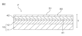
- the optical film F as an embodiment of the optical film with an antifouling layer of the present invention comprises a transparent base material 10, an optical functional layer 20, and an antifouling layer 30 in a thickness direction T. Prepare in this order toward one side.
- the optical film F includes a transparent base material 10, an adhesion layer 41, an optical functional layer 20, and an antifouling layer 30 in this order toward one side in the thickness direction T.
- the optical film F has a shape that spreads in a direction (plane direction) orthogonal to the thickness direction T.
- the transparent base material 10 is provided with the resin film 11 and the hard coat layer 12 in this order toward one side in the thickness direction T.
- the resin film 11 is a transparent resin film having flexibility.
- the material of the resin film 11 include polyester resin, polyolefin resin, polystyrene resin, acrylic resin, polycarbonate resin, polyether sulfone resin, polysulfone resin, polyamide resin, polyimide resin, cellulose resin, norbornene resin, polyarylate resin, and Polyvinyl alcohol resin can be mentioned.
- the polyester resin include polyethylene terephthalate (PET), polybutylene terephthalate, and polyethylene naphthalate.
- Polyolefin resins include, for example, polyethylene, polypropylene, and cycloolefin polymers (COPs).
- the cellulose resin include triacetyl cellulose (TAC).
- the material of the resin film 11 one selected from the group consisting of polyester resin, polyolefin resin, and cellulose resin is used from the viewpoint of transparency and strength, and more preferably, the group consisting of PET, COP, and TAC. The one selected from is used.
- the surface of the resin film 11 on the hard coat layer 12 side may be surface-modified.
- Examples of the surface modification treatment include corona treatment, plasma treatment, ozone treatment, primer treatment, glow treatment, and coupling agent treatment.
- the thickness of the resin film 11 is preferably 5 ⁇ m or more, more preferably 10 ⁇ m or more, and further preferably 20 ⁇ m or more.
- the thickness of the resin film 11 is preferably 300 ⁇ m or less, more preferably 200 ⁇ m or less, from the viewpoint of handleability.
- the total light transmittance (JIS K 7375-2008) of the resin film 11 is preferably 80% or more, more preferably 90% or more, still more preferably 95% or more. Such a configuration is suitable for ensuring the transparency required for the optical film F when the optical film F is provided on the surface of a display such as a touch panel display.
- the total light transmittance of the resin film 11 is, for example, 100% or less.
- the hard coat layer 12 is arranged on one surface of the resin film 11 in the thickness direction T.
- the hard coat layer 12 is a layer for making it difficult for scratches to be formed on the exposed surface (upper surface in FIG. 1) of the optical film F.
- the hard coat layer 12 is a cured product of the curable resin composition.
- the curable resin contained in the curable resin composition include polyester resin, acrylic resin, urethane resin, acrylic urethane resin, amide resin, silicone resin, epoxy resin, and melamine resin. These curable resins may be used alone or in combination of two or more. From the viewpoint of ensuring high hardness of the hard coat layer 12, an acrylic urethane resin is preferably used as the curable resin.
- examples of the curable resin composition include an ultraviolet curable resin composition and a thermosetting resin composition.
- an ultraviolet curable resin composition is preferably used from the viewpoint of helping to improve the production efficiency of the optical film F because it can be cured without heating at a high temperature.
- the UV curable resin composition contains at least one selected from the group consisting of UV curable monomers, UV curable oligomers, and UV curable polymers.
- Specific examples of the ultraviolet curable resin composition include the composition for forming a hard coat layer described in JP-A-2016-179686.
- the curable resin composition may contain fine particles.
- the formulation of the fine particles in the curable resin composition is useful for adjusting the hardness, adjusting the surface roughness, adjusting the refractive index, and imparting antiglare property in the hard coat layer 12.
- the fine particles include metal oxide particles, glass particles, and organic particles.
- Materials for the metal oxide particles include, for example, silica, alumina, titania, zirconia, calcium oxide, tin oxide, indium oxide, cadmium oxide, and antimony oxide.
- Materials for organic particles include, for example, polymethylmethacrylate, polystyrene, polyurethane, acrylic-styrene copolymers, benzoguanamines, melamines, and polycarbonates.
- the thickness of the hard coat layer 12 is preferably 1 ⁇ m or more, more preferably 3 ⁇ m or more, still more preferably 5 ⁇ m or more, from the viewpoint of ensuring the hardness of the surface of the antifouling layer 30 by ensuring the hardness of the hard coat layer 12.
- the thickness of the hard coat layer 12 is preferably 50 ⁇ m or less, more preferably 40 ⁇ m or less, still more preferably 35 ⁇ m or less, and particularly preferably 30 ⁇ m or less, from the viewpoint of ensuring the flexibility of the optical film F.
- the surface of the hard coat layer 12 on the adhesion layer 41 side may be surface-modified.
- Examples of the surface modification treatment include plasma treatment, corona treatment, ozone treatment, primer treatment, glow treatment, and coupling agent treatment. From the viewpoint of ensuring a high adhesion between the hard coat layer 12 and the adhesion layer 41, the surface of the hard coat layer 12 on the adhesion layer 41 side is preferably plasma-treated.
- the thickness of the transparent substrate 10 is preferably 5 ⁇ m or more, more preferably 10 ⁇ m or more, and further preferably 20 ⁇ m or more.
- the thickness of the transparent substrate 10 is preferably 300 ⁇ m or less, more preferably 200 ⁇ m or less, from the viewpoint of handleability.
- the total light transmittance (JIS K 7375-2008) of the transparent base material 10 is preferably 80% or more, more preferably 90% or more, still more preferably 95% or more. Such a configuration is suitable for ensuring the transparency required for the optical film F when the optical film F is provided on the surface of a display such as a touch panel display.
- the total light transmittance of the transparent substrate 10 is, for example, 100% or less.
- the adhesion layer 41 is a layer for ensuring the adhesion of the inorganic oxide layer (first high-refractive index layer 21 described later in this embodiment) to the transparent base material 10 (hard coat layer 12 in this embodiment). ..
- the adhesion layer 41 is arranged on one surface of the hard coat layer 12 in the thickness direction T.
- Examples of the material of the adhesion layer 41 include metals such as silicon, indium, nickel, chromium, aluminum, tin, gold, silver, platinum, zinc, titanium, tungsten, zirconium, and palladium, and two or more alloys of these metals. And the oxides of these metals are mentioned.
- both the adhesion to both the organic layer (specifically, the hard coat layer 12) and the inorganic oxide layer (specifically, the first high-refractive index layer 21 in this embodiment) and the transparency of the adhesion layer 41 are compatible.
- indium tin oxide (ITO) or silicon oxide (SiOx) is preferably used as the material of the adhesion layer 41.
- SiOx having a smaller oxygen content than the stoichiometric composition is preferably used, and more preferably SiOx having x of 1.2 or more and 1.9 or less is used. ..
- the thickness of the adhesion layer 41 ensures both the adhesion between the hard coat layer 12 and the inorganic oxide layer (first high-refractive index layer 21 in this embodiment) and the transparency of the adhesion layer 41. From the viewpoint, it is preferably 1 nm or more, and preferably 10 nm or less.
- the optical functional layer 20 is arranged on one surface of the adhesion layer 41 in the thickness direction T.
- the optical functional layer 20 is an antireflection layer for suppressing the reflection intensity of external light. That is, the optical film F is an antireflection film in this embodiment.
- the optical functional layer 20 (antireflection layer) has a high refractive index layer having a relatively large refractive index and a low refractive index layer having a relatively small refractive index alternately in the thickness direction.
- the net reflected light intensity is attenuated by the interference action between the reflected light at the plurality of interfaces in the plurality of thin layers (high refractive index layer, low refractive index layer).
- an interference effect for attenuating the reflected light intensity can be exhibited by adjusting the optical film thickness (product of the refractive index and the thickness) of each thin layer.
- the optical functional layer 20 as such an antireflection layer includes a first high refractive index layer 21, a first low refractive index layer 22, a second high refractive index layer 23, and a second low refractive index.
- the rate layer 24 is provided in this order toward one side of the thickness direction T.
- the first high-refractive index layer 21 and the second high-refractive index layer 23 are each made of a high-refractive index material having a refractive index of preferably 1.9 or more at a wavelength of 550 nm.
- high refractive index materials include, for example, niobium oxide (Nb 2 O 5 ), titanium oxide, zirconium oxide, tin-doped indium oxide (ITO), and antimony.
- Dope tin oxide (ATO) is mentioned, and niobium oxide is preferably used.
- the optical film thickness (product of refractive index and thickness) of the first high refractive index layer 21 is, for example, 20 nm or more, and is, for example, 55 nm or less.
- the optical film thickness of the second high-refractive index layer 23 is, for example, 60 nm or more, and for example, 330 nm or less.
- the first low refractive index layer 22 and the second low refractive index layer 24 are each made of a low refractive index material having a refractive index of preferably 1.6 or less at a wavelength of 550 nm.
- examples of the low refractive index material include silicon dioxide (SiO 2 ) and magnesium fluoride, and silicon dioxide is preferably used.
- the optical film thickness of the first low refractive index layer 22 is, for example, 15 nm or more, and is, for example, 70 nm or less.
- the optical film thickness of the second low refractive index layer 24 is, for example, 100 nm or more, and is, for example, 160 nm or less.
- the thickness of the first high refractive index layer 21 is, for example, 1 nm or more, preferably 5 nm or more, and for example, 30 nm or less, preferably 20 nm or less.
- the thickness of the first low refractive index layer 22 is, for example, 10 nm or more, preferably 20 nm or more, and for example, 50 nm or less, preferably 30 nm or less.
- the thickness of the second high refractive index layer 23 is, for example, 50 nm or more, preferably 80 nm or more, and for example, 200 nm or less, preferably 150 nm or less.
- the thickness of the second low refractive index layer 24 is, for example, 50 nm or more, preferably 60 nm or more, and for example, 150 nm or less, preferably 100 nm or less.
- the second low refractive index layer 24 also serves as an inorganic oxide base layer (inorganic oxide base layer 42) that ensures the peeling resistance of the antifouling layer 30.
- the material of the second low refractive index layer 24 include silicon dioxide and magnesium fluoride from the viewpoint of ensuring adhesion to the antifouling layer 30, and silicon dioxide is preferably used.
- the thickness of the second low refractive index layer 24 is preferably 50 nm or more, more preferably 65 nm or more, still more preferably 80 nm or more, and particularly preferably 90 nm or more. be. The same thickness is, for example, 150 nm or less.
- the surface of the inorganic oxide base layer 42 on the antifouling layer 30 side may be surface-modified.
- Examples of the surface modification treatment include corona treatment, plasma treatment, ozone treatment, primer treatment, glow treatment, and coupling agent treatment.
- the surface roughness Ra (arithmetic mean surface roughness) of the surface of the inorganic oxide base layer 42 on the antifouling layer 30 side is preferably 0.5 nm or more, more preferably 0.8 nm or more.
- the surface roughness Ra is preferably 10 nm or less, more preferably 8 nm or less.
- the surface roughness Ra is obtained from, for example, an observation image of 1 ⁇ m square by an AFM (atomic force microscope).
- the antifouling layer 30 is a layer having an antifouling function.
- the antifouling layer 30 is arranged on one surface of the inorganic oxide base layer 42 in the thickness direction T.
- the antifouling layer 30 has a surface 31 (outer surface) on one side in the thickness direction T.
- the antifouling function of the antifouling layer 30 includes a function of suppressing the adhesion of contaminants such as hand grease to the exposed surface of the film when the optical film F is used, and a function of facilitating the removal of the adhered contaminants.
- Examples of the material of the antifouling layer 30 include organic fluorine compounds.
- an alkoxysilane compound having a perfluoropolyether group is preferably used.
- Examples of the alkoxysilane compound having a perfluoropolyether group include a compound represented by the following general formula (1).
- R 1 is a linear or branched alkyl fluoride group in which one or more hydrogen atoms in the alkyl group are replaced with a fluorine atom (for example, the number of carbon atoms is 1 or more and 20 or less).
- R 2 represents a structure containing at least one repeating structure of a perfluoropolyether (PFPE) group, and preferably represents a structure containing two repeating structures of a PFPE group.
- the repeating structure of the PFPE group include a repeating structure of a linear PFPE group and a repeating structure of a branched PFPE group.
- the repeating structure of the linear PFPE group for example, a structure represented by- (OC n F 2n) p- (n represents an integer of 1 or more and 20 or less, and p is an integer of 1 or more and 50 or less. Represented. The same shall apply hereinafter).
- Examples of the repeating structure of the branched PFPE group include a structure represented by-(OC (CF 3 ) 2 ) p- and a structure represented by-(OCF 2 CF (CF 3 ) CF 2 ) p-. Can be mentioned.
- the repeating structure of the PFPE group is preferably a repeating structure of a linear PFPE group, and more preferably- (OCF 2 ) p- and-(OC 2 F 4 ) p- .
- R 3 represents an alkyl group having 1 or more and 4 or less carbon atoms, and preferably represents a methyl group.
- X represents an ether group, a carbonyl group, an amino group, or an amide group, and preferably represents an ether group.
- M represents an integer of 1 or more. Further, m represents an integer of preferably 20 or less, more preferably 10 or less, still more preferably 5 or less.
- the compound represented by the following general formula (2) is preferably used.
- q represents an integer of 1 or more and 50 or less
- r represents an integer of 1 or more and 50 or less
- alkoxysilane compound having a perfluoropolyether group may be used alone or in combination of two or more.
- the ratio of F to Si detected by elemental analysis of the antifouling layer 30 surface 31 (the surface of the antifouling layer 30 opposite to the transparent substrate 10) by X-ray photoelectron spectroscopy (F / Si, atoms).
- the number ratio) is 20 or more, preferably 22 or more, more preferably 24 or more, and further preferably 26 or more at an analysis depth of 1 nm.
- the antifouling layer 30 contains an alkoxysilane compound having a perfluoropolyether group, the higher the orientation of the compound having the following orientation, the more the compound having such orientation. The higher the number, the higher the above ratio.
- the orientation means that the alkyl fluoride group (preferably a perfluoroalkyl group) at one end of the long-chain structure of the compound is located on the surface 31 side, and the alkoxysilane structure portion at the other end is located on the optical functional layer 20 side.
- the orientation is preferably such that the long chain structure extends along the thickness direction T.
- the ratio of F to Si (F / Si) of the surface 31 of the antifouling layer 30 detected by elemental analysis by X-ray photoelectron spectroscopy preferably decreases monotonically from an analysis depth of 1 nm to an analysis depth of 5 nm. ..
- the antifouling layer 30 contains an alkoxysilane compound having a perfluoropolyether group, the higher the orientation of the same compound having the above orientation, and the more the same compound having the above orientation, the more the said.
- the degree of change in monotonous decrease is large.
- the elemental analysis of the antifouling layer 30 by X-ray photoelectron spectroscopy is specifically carried out as described later with respect to Examples.
- a method for adjusting the ratio (F / Si) for example, selection of the type of the organic fluorine compound, adjustment of the content ratio of the organic fluorine compound in the antifouling layer 30, selection of a method for forming the antifouling layer 30;
- the selection of the material of the base layer of the antifouling layer 30 (the second low refractive index layer 24 in the present embodiment) and the adjustment of the surface roughness of the surface of the base layer on the antifouling layer 30 side can be mentioned.
- a step of forming the base layer (second low refractive index layer 24 in the present embodiment) for the antifouling layer 30 and a step of forming the antifouling layer 30 on the base layer 30 are used. Also included is the choice of whether or not to perform in a series of roll-to-roll lines (ie, without winding the work film between the two steps).
- the antifouling layer 30 is a film (dry coating film) formed by the dry coating method in the present embodiment.
- the dry coating method include a sputtering method, a vacuum vapor deposition method, and a CVD method.
- the antifouling layer 30 is preferably a dry coating film, and more preferably a vacuum-deposited film.
- the structure in which the material of the antifouling layer 30 contains an alkoxysilane compound having a perfluoropolyether group and the antifouling layer 30 is a dry coating film (preferably a vacuum-deposited film) is relative to the optical functional layer 20. It is suitable for ensuring a high bonding force of the antifouling layer 30, and therefore suitable for ensuring the peeling resistance of the antifouling layer 30.
- the high peel resistance of the antifouling layer 30 helps maintain the antifouling function of the antifouling layer 30.
- the water contact angle (pure water contact angle) of the outer surface 31 of the antifouling layer 30 is 110 ° or more, preferably 111 ° or more, more preferably 112 ° or more, still more preferably 113 ° or more, and particularly preferably 114 °. It is above °.
- the configuration in which the water contact angle on the outer surface 31 is as high as this is suitable for realizing high antifouling property in the antifouling layer 30.
- the water contact angle is, for example, 130 ° or less.
- the water contact angle is determined by forming water droplets (droplets of pure water) having a diameter of 2 mm or less on the outer surface 31 (exposed surface) of the antifouling layer 30 and measuring the contact angle of the water droplets with respect to the surface of the antifouling layer 30. Is required by.
- the water contact angle of the outer surface 31 is, for example, the composition of the antifouling layer 30, the roughness of the outer surface 31, the composition of the hard coat layer 12, and the roughness of the surface of the hard coat layer 12 on the optical functional layer 20 side. It can be adjusted by adjustment.
- the thickness of the antifouling layer 30 is preferably 1 nm or more, more preferably 3 nm or more, further preferably 5 nm or more, and particularly preferably 7 nm or more. Such a configuration is suitable for ensuring the peeling resistance of the antifouling layer 30.
- the thickness of the antifouling layer 30 is preferably 25 nm or less, more preferably 20 nm or less, still more preferably 18 nm or less. Such a configuration is suitable for realizing the above-mentioned water contact angle in the antifouling layer 30.
- the adhesion layer 41, the optical functional layer 20, and the antifouling layer 30 are sequentially laminated on the transparent base material 10.
- the optical functional layer 20 is formed by sequentially laminating a first high refractive index layer 21, a first low refractive index layer 22, a second high refractive index layer 23, and a second low refractive index layer 24 on the close contact layer 41. Can be formed.
- the transparent base material 10 can be produced by forming the hard coat layer 12 on the resin film 11.
- the hard coat layer 12 is formed by, for example, applying a curable resin composition containing a curable resin and, if necessary, fine particles on a resin film 11 to form a coating film, and then curing the coating film. Can be formed by.
- the curable resin composition contains an ultraviolet-type resin
- the coating film is cured by irradiation with ultraviolet rays.
- the curable resin composition contains a thermosetting resin
- the coating film is cured by heating.
- the exposed surface of the hard coat layer 12 formed on the transparent base material 10 is surface-modified as necessary (hard coat layer pretreatment step).
- the treatment gas include argon gas and oxygen gas.
- the discharge power in the plasma processing is, for example, 10 W or more, and for example, 10000 W or less.
- the adhesion layer 41, the first high refractive index layer 21, the first low refractive index layer 22, the second high refractive index layer 23, and the second low refractive index layer 24 are each sequentially formed by a dry coating method. It can be formed by (dry film formation step). Examples of the dry coating method include a sputtering method, a vacuum vapor deposition method, and a CVD method, and a sputtering method is preferably used.
- a negative voltage is applied to a target arranged on the cathode while introducing a gas into the sputtering chamber under vacuum conditions.
- a glow discharge is generated to ionize the gas atom, the gas ion collides with the target surface at high speed, the target material is ejected from the target surface, and the ejected target material is deposited on a predetermined surface.
- reactive sputtering is preferable as the sputtering method.
- a metal target is used as the target, and a mixed gas of an inert gas such as argon and oxygen (reactive gas) is used as the above-mentioned gas.
- Examples of the power supply for carrying out the sputtering method include a DC power supply, an AC power supply, an RF power supply, and an MFAC power supply (AC power supply having a frequency band of several kHz to several MHz).
- the discharge voltage in the sputtering method is, for example, 200 V or more, and is, for example, 1000 V or less.
- the film forming pressure in the sputtering chamber where the sputtering method is carried out is, for example, 0.01 Pa or more, and is, for example, 2 Pa or less.
- the exposed surface of the antireflection layer is surface-modified as necessary (base layer pretreatment step).
- the treatment gas include oxygen gas and argon gas, and oxygen gas is preferably used.
- the discharge power in the plasma processing is, for example, 10 W or more, preferably 50 W or more, and more preferably 70 W or more.
- the discharge power is, for example, 10000 W or less, preferably 8000 W or less, more preferably 5000 W or less, still more preferably 4000 W or less, and particularly preferably 3000 W or less.
- the antifouling layer 30 can be formed by forming the above-mentioned organic fluorine compound on the optical functional layer 20 (antifouling layer forming step).
- Examples of the method for forming the antifouling layer 30 include a dry coating method.
- Examples of the dry coating method include a vacuum vapor deposition method, a sputtering method, and a CVD method, and a vacuum vapor deposition method is preferably used.
- a series of processes from the dry film forming step to the antifouling layer forming step is carried out in one continuous line while running the work film by the roll-to-roll method. More preferably, a series of processes from the hard coat layer pretreatment step to the antifouling layer forming step is carried out in one continuous line while running the work film in a roll-to-roll method. During the process on one continuous line, the work film is never exposed to the atmosphere and is preferably not rolled into a roll.
- the optical film F can be manufactured as described above.
- the optical film F is used with the transparent base material 10 side bonded to the adherend via, for example, an adhesive.
- the adherend include a transparent cover arranged on the image display side of a display such as a touch panel display.
- the ratio of F to Si (F / Si, atomic number ratio) of the surface 31 of the antifouling layer 30 to Si detected by elemental analysis by X-ray photoelectron spectroscopy is the analysis depth. At 1 nm, it is 20 or more, preferably 22 or more, more preferably 24 or more, and further preferably 26 or more. Further, the ratio preferably decreases monotonically from an analysis depth of 1 nm to an analysis depth of 5 nm. These configurations are suitable for exhibiting excellent antifouling property on the surface 31 by superimposing high hydrophobicity and high oleophobicity due to the terminal fluoroalkyl group of the organic fluorine compound.
- the above configuration regarding the ratio (F / Si) is suitable for ensuring a state in which the terminal fluoride alkyl group is densely arranged with high orientation on the surface 31.
- the optical film F may be an optical film other than the antireflection film.
- optical films include transparent conductive films and electromagnetic wave shielding films.
- the optical functional layer 20 of the optical film F has, for example, a first dielectric thin film, a transparent electrode film such as an ITO film, and a second dielectric film. Prepare in this order toward one side of the direction T.
- the optical functional layer 20 having such a laminated structure both visible light transmission and conductivity are compatible.
- the optical functional layer 20 of the optical film F is provided with, for example, a metal thin film having an electromagnetic wave reflecting ability and a metal oxide film alternately in the thickness direction T.
- the optical functional layer 20 having such a laminated structure both shielding property against electromagnetic waves having a specific wavelength and visible light transmission property are compatible.
- the optical film F does not have to include the optical functional layer 20.
- the transparent base material 10 resin film 11, hard coat layer 12
- the adhesion layer 41 the inorganic oxide base layer 42
- the antifouling layer 30 are formed in the thickness direction T. Prepare in this order toward one side.
- the inorganic oxide base layer 42 is arranged on the adhesion layer 41.
- the present invention will be specifically described below with reference to examples.
- the present invention is not limited to the examples.
- the specific numerical values such as the compounding amount (content), the physical property value, the parameter, etc. described below are the compounding amounts corresponding to them described in the above-mentioned "form for carrying out the invention” (forms for carrying out the invention). It can be replaced with the upper limit (numerical value defined as “less than or equal to” or “less than”) or lower limit (numerical value defined as "greater than or equal to” or “greater than or equal to”) such as content), physical property value, and parameter.
- a hard coat layer was formed on one side of a long triacetyl cellulose (TAC) film (thickness 80 ⁇ m) as a transparent resin film (hard coat layer forming step).
- TAC triacetyl cellulose
- this step first, 100 parts by mass of an ultraviolet curable acrylic monomer (trade name "GRANDIC PC-1070", manufactured by DIC) and an organosilica sol containing nanosilica particles (trade name "MEK-ST-L", nanosilica)
- the average primary particle size of the particles is 50 nm, the solid content concentration is 30% by mass, manufactured by Nissan Chemical Co., Ltd.
- a high-pressure mercury lamp was used as a light source, ultraviolet rays having a wavelength of 365 nm were used, and the integrated irradiation light amount was set to 200 mJ / cm 2 .
- the heating time was 80 ° C., and the heating temperature was 3 minutes.
- HC hard coat
- the surface of the HC layer of the film was plasma-treated by a plasma processing device in a vacuum atmosphere of 1.0 Pa (HC layer pretreatment). Process).
- argon gas was used as the treatment gas, and the discharge power (discharge output) was set to 150 W.
- an adhesion layer and an antireflection layer were sequentially formed on the HC layer of the TAC film with the HC layer after the plasma treatment (sputter film formation step).
- a roll-to-roll spatter film forming apparatus is used to provide an indium tin oxide (ITO) layer with a thickness of 1.5 nm as an adhesion layer on the HC layer of the TAC film with an HC layer, and the first height.
- ITO indium tin oxide
- an ITO target is used, an argon gas as an inert gas and 10 parts by volume of oxygen gas as a reactive gas with respect to 100 parts by volume of the argon gas are used, and the discharge voltage is set to 400 V.
- the pressure in the film chamber was 0.2 Pa, and the ITO layer was formed by MFAC sputtering.
- an Nb target is used, 100 parts by volume of argon gas and 5 parts by volume of oxygen gas are used, the discharge voltage is 415 V, the film formation pressure is 0.42 Pa, and Nb is formed by MFAC sputtering. the 2 O 5 layer was formed.
- a Si target is used, 100 parts by volume of argon gas and 30 parts by volume of oxygen gas are used, the discharge voltage is 350 V, the film formation pressure is 0.3 Pa, and SiO is used by MFAC sputtering. Two layers were formed.
- an Nb target is used, 100 parts by volume of argon gas and 13 parts by volume of oxygen gas are used, the discharge voltage is 460 V, the film formation pressure is 0.5 Pa, and Nb is Nb by MFAC sputtering. the 2 O 5 layer was formed.
- a Si target is used, 100 parts by volume of argon gas and 30 parts by volume of oxygen gas are used, the discharge voltage is 340 V, the film formation pressure is 0.25 Pa, and SiO is used by MFAC sputtering. Two layers were formed.
- the antireflection layer (first high refractive index layer, first low refractive index layer, second high refractive index layer, second low) is placed on the HC layer of the TAC film with the HC layer via the adhesion layer.
- the refractive index layer was laminated and formed.
- the surface of the formed antireflection layer was plasma-treated with a plasma processing device in a vacuum atmosphere of 1.0 Pa (underlayer pretreatment step).
- oxygen gas was used as the treatment gas, and the discharge power was set to 100 W.
- an antifouling layer was formed on the antireflection layer (antifouling layer forming step). Specifically, an antifouling layer having a thickness of 8 nm was formed on the antireflection layer by a vacuum vapor deposition method using an alkoxysilane compound containing a perfluoropolyether group as a vapor deposition source.
- the vapor deposition source is a solid content obtained by drying "Optur UD509" manufactured by Daikin Industries, Ltd. (perfluoropolyether group-containing alkoxysilane compound represented by the above general formula (2), solid content concentration 20% by mass). be.
- the heating temperature of the vapor deposition source in the vacuum vapor deposition method was 260 ° C.
- the optical film of Example 1 was produced.
- the optical film of Example 1 is provided with a transparent base material (resin film, hard coat layer), an adhesion layer, an antireflection layer, and an antifouling layer in this order toward one side in the thickness direction.
- Example 2 An optical film of Example 2 was produced in the same manner as the optical film of Example 1 except for the following.
- the underlayer pretreatment step was not carried out (that is, the discharge power of the plasma treatment as the underlayer pretreatment was set to 0 W).
- the antifouling layer forming step vacuum vapor deposition
- Comparative Example 1 The optical film of Comparative Example 1 was produced in the same manner as the optical film of Example 1 except that the work film was once wound into a roll shape after the base layer pretreatment step and before the antifouling layer forming step. did.
- Comparative Example 2 An optical film of Comparative Example 2 was produced in the same manner as the optical film of Example 1 except for the antifouling layer forming step.
- the antifouling layer was formed by the wet coating method. Specifically, first, "Optur UD509" (manufactured by Daikin Industries, Ltd.) as a coating agent is diluted with a diluting solvent (trade name "Fluorinert", manufactured by 3M Co., Ltd.) to obtain a solid content concentration of 0.1% by mass. A coating solution was prepared. Next, a coating liquid was applied by gravure coating on the antireflection layer formed in the sputtering film formation step to form a coating film. The coating was then dried by heating at 60 ° C. for 2 minutes. As a result, an antifouling layer having a thickness of 7 nm was formed on the antireflection layer.
- the sample for analysis was prepared by cutting out from an optical film to a size of about 10 mm ⁇ 10 mm.
- An X-ray photoelectron spectrometer (trade name "Quantum 2000", manufactured by ULVAC-PHI, Inc.) was used for the analysis. In this analysis, X-ray photoelectron spectroscopy was performed under the following conditions.
- Excited X-ray source Monochrome AI K ⁇ X-ray Settinng: 200 ⁇ m ⁇ (15 kV, 30 W) Photoelectron extraction angle: 5 degrees, 15 degrees, 30 degrees, 45 degrees with respect to the sample surface
- the analysis depth was adjusted by adjusting the photoelectron extraction angle. Specifically, the analysis depth is set to 1 nm by setting the photoelectron extraction angle to 5 degrees, the analysis depth is set to 2 nm by setting the photoelectron extraction angle to 15 degrees, and the analysis is performed by setting the photoelectron extraction angle to 30 degrees. By setting the depth to 3 nm and the photoelectron extraction angle to 45 degrees, the analysis depth was set to 5 nm.
- the elemental analysis results are shown in Table 1.
- the ratio of F to the detected Si is also shown in Table 1.
- ⁇ Eraser sliding test> For each of the optical films of Examples 1 and 2 and Comparative Examples 1 and 2, the degree of deterioration of the antifouling property on the surface of the antifouling layer by passing through the eraser sliding test was investigated. Specifically, first, a sliding test was carried out in which the eraser was reciprocated while sliding the eraser against the surface of the antifouling layer of the optical film. In this test, an eraser ( ⁇ 6 mm) manufactured by Minoan was used, the load of the eraser on the surface of the antifouling layer was 1 kg / 6 mm ⁇ , and the sliding distance of the eraser on the surface of the antifouling layer (one way in reciprocating movement) was 20 mm.
- the sliding speed of the eraser was set to 40 rpm, and the number of times the eraser was reciprocated with respect to the surface of the antifouling layer was set to 3000 reciprocations.
- the water contact angle of the eraser sliding portion on the surface of the antifouling layer of the optical film was measured by the same method as the initial measurement method of the water contact angle ⁇ 0.
- the measurement results are shown in Table 1 as the water contact angle ⁇ 1 after the eraser sliding test.
- the degree of decrease in the water contact angle on the surface of the antifouling layer due to the eraser sliding test is significantly smaller than that of the optical films of Comparative Examples 1 and 2, therefore.
- the decrease in antifouling property is significantly small (on the surface of the antifouling layer, the smaller the decrease in water contact angle, the smaller the decrease in antifouling property).
- the optical film with an antifouling layer of the present invention can be applied to, for example, an antireflection film with an antifouling layer, a transparent conductive film with an antifouling layer, and an electromagnetic wave shielding film with an antifouling layer.
- Optical film (optical film with antifouling layer) 10 Transparent base material 11 Resin film 12 Hard coat layer 20 Optical functional layer 21 First high refractive index layer 22 First low refractive index layer 23 Second high refractive index layer 24 Second low refractive index layer 30 Antifouling layer 31 Surface 41 Adhesion layer 42 Inorganic oxide base layer T Thickness direction
Abstract
Description
反応性スパッタリングでは、ターゲットとして金属ターゲットを用い、上述のガスとして、アルゴンなどの不活性ガスと酸素(反応性ガス)との混合ガスを用いる。不活性ガスと酸素との流量比(sccm)の調整により、成膜される無機酸化物に含まれる酸素の割合を調整できる。
まず、透明な樹脂フィルムとしての長尺のトリアセチルセルロース(TAC)フィルム(厚さ80μm)の片面に、ハードコート層を形成した(ハードコート層形成工程)。本工程では、まず、紫外線硬化型のアクリルモノマー(商品名「GRANDIC PC-1070」,DIC社製)100質量部と、ナノシリカ粒子を含有するオルガノシリカゾル(商品名「MEK-ST-L」,ナノシリカ粒子の平均一次粒子径は50nm,固形分濃度30質量%,日産化学社製)25質量部(ナノシリカ粒子換算量)と、チキソトロピー付与剤(商品名「ルーセンタイトSAN」,有機粘土である合成スメクタイト,コープケミカル社製)1.5質量部と、光重合開始剤(商品名「OMNIRAD907」,BASF社製)3質量部と、レベリング剤(商品名「LE303」,共栄社化学社製)0.15質量部とを混合して、固形分濃度55質量%の組成物(ワニス)を調製した。混合には、超音波分散機を使用した。次に、上記TACフィルムの片面に組成物を塗布して塗膜を形成した。次に、この塗膜を、紫外線照射により硬化させた後、加熱により乾燥させた。紫外線照射では、光源として高圧水銀ランプを使用し、波長365nmの紫外線を用い、積算照射光量を200mJ/cm2とした。また、加熱の時間は80℃とし、加熱の温度は3分間とした。これにより、TACフィルム上に厚さ6μmのハードコート(HC)層を形成した。
次のこと以外は、実施例1の光学フィルムと同様にして、実施例2の光学フィルムを作製した。下地層前処理工程を実施しなかった(即ち、下地層前処理としてのプラズマ処理の放電電力は0Wとした)。防汚層形成工程(真空蒸着)において、蒸着源として、信越化学社製の「KY1903-1」(パーフルオロポリエーテル基含有アルコキシシラン化合物)を乾燥して得た固形分を用いた。
下地層前処理工程後であって防汚層形成工程前に、ワークフィルムを一旦 ロール状に巻き取ったこと以外は、実施例1の光学フィルムと同様にして、比較例1の光学フィルムを作製した。
防汚層形成工程以外は、実施例1の光学フィルムと同様にして、比較例2の光学フィルムを作製した。本比較例の防汚層形成工程では、ウェットコーティング法によって防汚層を形成した。具体的には、まず、コーティング剤としての「オプツール UD509」(ダイキン工業社製)を、希釈溶媒(商品名「フロリナート」,3M社製)で希釈して、固形分濃度0.1質量%のコーティング液を調製した。次に、スパッタ成膜工程で形成された反射防止層の上に、コーティング液をグラビアコーティングによって塗布して塗膜を形成した。次に、この塗膜を、60℃で2分間の加熱によって乾燥させた。これにより、反射防止層上に厚さ7nmの防汚層を形成した。
実施例1,2および比較例1,2の各光学フィルムの防汚層表面を、X線光電子分光法(ESCA)によって分析した。分析用の試料は、光学フィルムから10mm×10mm程度のサイズに切り出して用意した。分析には、X線光電子分光装置(商品名「Quantum 2000」,アルバック・ファイ社製)を使用した。本分析では、下記の条件でX線光電子分光測定を行った。
X-ray Settinng:200μmφ(15kV,30W)
光電子取り出し角:試料表面に対して5度、15度、30度、45度
実施例1,2および比較例1,2の各光学フィルムについて、防汚層表面の水接触角を調べた。まず、光学フィルムの防汚層表面に、約1μLの純水の滴下によって水滴を形成した。次に、防汚層表面上の水滴の表面と防汚層表面とがなす角度を測定した。測定には、接触角計(商品名「DMo-501」,協和界面科学社製)を使用した。その測定結果を、初期の水接触角θ0として表1に示す。
実施例1,2および比較例1,2の各光学フィルムについて、消しゴム摺動試験を経ることによる防汚層表面の防汚性低下の程度を調べた。具体的には、まず、光学フィルムの防汚層表面に対して消しゴムを摺動させつつ往復動させる摺動試験を実施した。この試験では、Minoan社製の消しゴム(Φ6mm)を使用し、防汚層表面に対する消しゴムの荷重を1kg/6mmΦとし、防汚層表面上の消しゴムの摺動距離(往復動における片道)を20mmとし、消しゴムの摺動速度を40rpmとし、防汚層表面に対して消しゴムを往復動させる回数は3000往復とした。次に、光学フィルムの防汚層表面における消しゴム摺動箇所の水接触角を、初期の水接触角θ0の測定方法と同様の方法で測定した。その測定結果を、消しゴム摺動試験後の水接触角θ1として、表1に示す。
実施例1,2の光学フィルムでは、比較例1,2の各光学フィルムと比較して、消しゴム摺動試験を経ることによる防汚層表面における水接触角の低下の程度が有意に小さく、従って、防汚性の低下が有意に小さい(防汚層表面では、水接触角の低下が小さいほど、防汚性の低下は小さい)。

10 透明基材
11 樹脂フィルム
12 ハードコート層
20 光学機能層
21 第1高屈折率層
22 第1低屈折率層
23 第2高屈折率層
24 第2低屈折率層
30 防汚層
31 表面
41 密着層
42 無機酸化物下地層
T 厚さ方向
Claims (7)
- 透明基材と防汚層とを厚さ方向に順に備え、
前記防汚層における前記透明基材とは反対の表面側の、X線光電子分光法での元素分析によって検出されるSiに対するFの比率が、分析深さ1nmでは20以上である、防汚層付き光学フィルム。 - 前記防汚層における前記比率が、分析深さ1nmから分析深さ5nmにかけて単調減少する、請求項1に記載の防汚層付き光学フィルム。
- 前記防汚層が、パーフルオロポリエーテル基を有するアルコキシシラン化合物を含有する、請求項1または2に記載の防汚層付き光学フィルム。
- 前記防汚層がドライコーティング膜である、請求項1から3のいずれか一つに記載の防汚層付き光学フィルム。
- 前記透明基材と前記防汚層との間に無機酸化物下地層を備え、当該無機酸化物下地層上に前記防汚層が配置されている、請求項1から4のいずれか一つに記載の防汚層付き光学フィルム。
- 前記無機酸化物下地層が二酸化ケイ素を含む、請求項5に記載の防汚層付き光学フィルム。
- 前記無機酸化物下地層における前記防汚層側の表面が、0.5nm以上10nm以下の表面粗さRaを有する、請求項5または6に記載の防汚層付き光学フィルム。
Priority Applications (4)
| Application Number | Priority Date | Filing Date | Title |
|---|---|---|---|
| JP2022536376A JP7169492B2 (ja) | 2020-07-13 | 2021-07-13 | 防汚層付き光学フィルム |
| KR1020227045624A KR102517502B1 (ko) | 2020-07-13 | 2021-07-13 | 방오층이 형성된 광학 필름 |
| CN202180046973.7A CN115916528B (zh) | 2020-07-13 | 2021-07-13 | 带防污层的光学薄膜 |
| JP2022172169A JP7219849B2 (ja) | 2020-07-13 | 2022-10-27 | 防汚層付き光学フィルム |
Applications Claiming Priority (10)
| Application Number | Priority Date | Filing Date | Title |
|---|---|---|---|
| JP2020-120131 | 2020-07-13 | ||
| JP2020120131 | 2020-07-13 | ||
| JP2020146144 | 2020-08-31 | ||
| JP2020-146144 | 2020-08-31 | ||
| JP2020166844 | 2020-10-01 | ||
| JP2020-166844 | 2020-10-01 | ||
| JP2020-166847 | 2020-10-01 | ||
| JP2020166847 | 2020-10-01 | ||
| JP2020-190468 | 2020-11-16 | ||
| JP2020190468 | 2020-11-16 |
Publications (1)
| Publication Number | Publication Date |
|---|---|
| WO2022014572A1 true WO2022014572A1 (ja) | 2022-01-20 |
Family
ID=79555574
Family Applications (1)
| Application Number | Title | Priority Date | Filing Date |
|---|---|---|---|
| PCT/JP2021/026250 WO2022014572A1 (ja) | 2020-07-13 | 2021-07-13 | 防汚層付き光学フィルム |
Country Status (5)
| Country | Link |
|---|---|
| JP (2) | JP7169492B2 (ja) |
| KR (1) | KR102517502B1 (ja) |
| CN (1) | CN115916528B (ja) |
| TW (1) | TWI811735B (ja) |
| WO (1) | WO2022014572A1 (ja) |
Citations (6)
| Publication number | Priority date | Publication date | Assignee | Title |
|---|---|---|---|---|
| JPH10232301A (ja) * | 1996-12-19 | 1998-09-02 | Nitto Denko Corp | 反射防止膜及び光学素材 |
| JP2000009906A (ja) * | 1998-06-23 | 2000-01-14 | Toppan Printing Co Ltd | 反射防止光学部材、防汚層の形成方法、光学機能性部材および表示装置 |
| JP2000144097A (ja) * | 1998-01-31 | 2000-05-26 | Toppan Printing Co Ltd | 防汚剤、防汚層の形成方法、光学部材、反射防止光学部材、光学機能性部材及び表示装置 |
| JP2002006103A (ja) * | 2000-06-23 | 2002-01-09 | Toppan Printing Co Ltd | 反射防止フィルム、光学機能性フィルム、及び表示装置 |
| JP2002243906A (ja) * | 2001-02-21 | 2002-08-28 | Toppan Printing Co Ltd | 反射防止積層体及びその製造方法 |
| JP2010210945A (ja) * | 2009-03-10 | 2010-09-24 | Seiko Epson Corp | 光学多層フィルムおよびその製造方法 |
Family Cites Families (6)
| Publication number | Priority date | Publication date | Assignee | Title |
|---|---|---|---|---|
| KR101173451B1 (ko) * | 2004-08-12 | 2012-08-13 | 후지필름 가부시키가이샤 | 반사방지 필름, 편광판 및 이를 이용한 화상 표시 장치 |
| WO2017086316A1 (ja) * | 2015-11-20 | 2017-05-26 | 旭硝子株式会社 | 膜付き曲げ基材およびその製造方法、ならびに画像表示装置 |
| JP6746410B2 (ja) * | 2016-07-13 | 2020-08-26 | 大日本印刷株式会社 | 光学積層体 |
| JP7133354B2 (ja) * | 2018-05-17 | 2022-09-08 | 日東電工株式会社 | 映り込み防止層付偏光板 |
| JP7217118B2 (ja) | 2018-09-26 | 2023-02-02 | 日東電工株式会社 | 保護フィルム付き光学フィルム |
| JP2020060657A (ja) * | 2018-10-09 | 2020-04-16 | 日東電工株式会社 | 反射防止ガラス |
-
2021
- 2021-07-13 JP JP2022536376A patent/JP7169492B2/ja active Active
- 2021-07-13 KR KR1020227045624A patent/KR102517502B1/ko active IP Right Grant
- 2021-07-13 WO PCT/JP2021/026250 patent/WO2022014572A1/ja active Application Filing
- 2021-07-13 CN CN202180046973.7A patent/CN115916528B/zh active Active
- 2021-07-13 TW TW110125727A patent/TWI811735B/zh active
-
2022
- 2022-10-27 JP JP2022172169A patent/JP7219849B2/ja active Active
Patent Citations (6)
| Publication number | Priority date | Publication date | Assignee | Title |
|---|---|---|---|---|
| JPH10232301A (ja) * | 1996-12-19 | 1998-09-02 | Nitto Denko Corp | 反射防止膜及び光学素材 |
| JP2000144097A (ja) * | 1998-01-31 | 2000-05-26 | Toppan Printing Co Ltd | 防汚剤、防汚層の形成方法、光学部材、反射防止光学部材、光学機能性部材及び表示装置 |
| JP2000009906A (ja) * | 1998-06-23 | 2000-01-14 | Toppan Printing Co Ltd | 反射防止光学部材、防汚層の形成方法、光学機能性部材および表示装置 |
| JP2002006103A (ja) * | 2000-06-23 | 2002-01-09 | Toppan Printing Co Ltd | 反射防止フィルム、光学機能性フィルム、及び表示装置 |
| JP2002243906A (ja) * | 2001-02-21 | 2002-08-28 | Toppan Printing Co Ltd | 反射防止積層体及びその製造方法 |
| JP2010210945A (ja) * | 2009-03-10 | 2010-09-24 | Seiko Epson Corp | 光学多層フィルムおよびその製造方法 |
Also Published As
| Publication number | Publication date |
|---|---|
| TWI811735B (zh) | 2023-08-11 |
| KR20230007543A (ko) | 2023-01-12 |
| KR102517502B1 (ko) | 2023-04-03 |
| JP2023010726A (ja) | 2023-01-20 |
| CN115916528B (zh) | 2024-03-12 |
| JPWO2022014572A1 (ja) | 2022-01-20 |
| JP7219849B2 (ja) | 2023-02-08 |
| TW202216426A (zh) | 2022-05-01 |
| CN115916528A (zh) | 2023-04-04 |
| JP7169492B2 (ja) | 2022-11-10 |
Similar Documents
| Publication | Publication Date | Title |
|---|---|---|
| WO2022014569A1 (ja) | 防汚層付き光学フィルム | |
| WO2022014568A1 (ja) | 防汚層付き光学フィルム | |
| WO2022014572A1 (ja) | 防汚層付き光学フィルム | |
| WO2022014570A1 (ja) | 防汚層付き光学フィルム | |
| WO2022014571A1 (ja) | 防汚層付き光学フィルム | |
| WO2022014573A1 (ja) | 防汚層付き光学フィルム | |
| JP2022079332A (ja) | 防汚層付き光学フィルム | |
| JP7389259B2 (ja) | 防汚層付き光学フィルム | |
| JP7186334B2 (ja) | 積層体 | |
| JP7186333B2 (ja) | 積層体 |
Legal Events
| Date | Code | Title | Description |
|---|---|---|---|
| 121 | Ep: the epo has been informed by wipo that ep was designated in this application |
Ref document number: 21842367 Country of ref document: EP Kind code of ref document: A1 |
|
| ENP | Entry into the national phase |
Ref document number: 2022536376 Country of ref document: JP Kind code of ref document: A |
|
| ENP | Entry into the national phase |
Ref document number: 20227045624 Country of ref document: KR Kind code of ref document: A |
|
| NENP | Non-entry into the national phase |
Ref country code: DE |
|
| 122 | Ep: pct application non-entry in european phase |
Ref document number: 21842367 Country of ref document: EP Kind code of ref document: A1 |