WO2022014319A1 - Substrat d'isolation, et procédé de fabrication de celui-ci - Google Patents
Substrat d'isolation, et procédé de fabrication de celui-ci Download PDFInfo
- Publication number
- WO2022014319A1 WO2022014319A1 PCT/JP2021/024584 JP2021024584W WO2022014319A1 WO 2022014319 A1 WO2022014319 A1 WO 2022014319A1 JP 2021024584 W JP2021024584 W JP 2021024584W WO 2022014319 A1 WO2022014319 A1 WO 2022014319A1
- Authority
- WO
- WIPO (PCT)
- Prior art keywords
- metal plate
- insulating substrate
- heat
- main surface
- circuit
- Prior art date
Links
Images


Classifications
-
- H—ELECTRICITY
- H01—ELECTRIC ELEMENTS
- H01L—SEMICONDUCTOR DEVICES NOT COVERED BY CLASS H10
- H01L23/00—Details of semiconductor or other solid state devices
- H01L23/34—Arrangements for cooling, heating, ventilating or temperature compensation ; Temperature sensing arrangements
- H01L23/36—Selection of materials, or shaping, to facilitate cooling or heating, e.g. heatsinks
- H01L23/373—Cooling facilitated by selection of materials for the device or materials for thermal expansion adaptation, e.g. carbon
- H01L23/3735—Laminates or multilayers, e.g. direct bond copper ceramic substrates
-
- C—CHEMISTRY; METALLURGY
- C04—CEMENTS; CONCRETE; ARTIFICIAL STONE; CERAMICS; REFRACTORIES
- C04B—LIME, MAGNESIA; SLAG; CEMENTS; COMPOSITIONS THEREOF, e.g. MORTARS, CONCRETE OR LIKE BUILDING MATERIALS; ARTIFICIAL STONE; CERAMICS; REFRACTORIES; TREATMENT OF NATURAL STONE
- C04B37/00—Joining burned ceramic articles with other burned ceramic articles or other articles by heating
- C04B37/02—Joining burned ceramic articles with other burned ceramic articles or other articles by heating with metallic articles
- C04B37/023—Joining burned ceramic articles with other burned ceramic articles or other articles by heating with metallic articles characterised by the interlayer used
- C04B37/026—Joining burned ceramic articles with other burned ceramic articles or other articles by heating with metallic articles characterised by the interlayer used consisting of metals or metal salts
-
- H—ELECTRICITY
- H01—ELECTRIC ELEMENTS
- H01L—SEMICONDUCTOR DEVICES NOT COVERED BY CLASS H10
- H01L23/00—Details of semiconductor or other solid state devices
- H01L23/34—Arrangements for cooling, heating, ventilating or temperature compensation ; Temperature sensing arrangements
- H01L23/36—Selection of materials, or shaping, to facilitate cooling or heating, e.g. heatsinks
- H01L23/373—Cooling facilitated by selection of materials for the device or materials for thermal expansion adaptation, e.g. carbon
- H01L23/3736—Metallic materials
-
- C—CHEMISTRY; METALLURGY
- C04—CEMENTS; CONCRETE; ARTIFICIAL STONE; CERAMICS; REFRACTORIES
- C04B—LIME, MAGNESIA; SLAG; CEMENTS; COMPOSITIONS THEREOF, e.g. MORTARS, CONCRETE OR LIKE BUILDING MATERIALS; ARTIFICIAL STONE; CERAMICS; REFRACTORIES; TREATMENT OF NATURAL STONE
- C04B2235/00—Aspects relating to ceramic starting mixtures or sintered ceramic products
- C04B2235/65—Aspects relating to heat treatments of ceramic bodies such as green ceramics or pre-sintered ceramics, e.g. burning, sintering or melting processes
- C04B2235/658—Atmosphere during thermal treatment
- C04B2235/6581—Total pressure below 1 atmosphere, e.g. vacuum
-
- C—CHEMISTRY; METALLURGY
- C04—CEMENTS; CONCRETE; ARTIFICIAL STONE; CERAMICS; REFRACTORIES
- C04B—LIME, MAGNESIA; SLAG; CEMENTS; COMPOSITIONS THEREOF, e.g. MORTARS, CONCRETE OR LIKE BUILDING MATERIALS; ARTIFICIAL STONE; CERAMICS; REFRACTORIES; TREATMENT OF NATURAL STONE
- C04B2237/00—Aspects relating to ceramic laminates or to joining of ceramic articles with other articles by heating
- C04B2237/02—Aspects relating to interlayers, e.g. used to join ceramic articles with other articles by heating
- C04B2237/12—Metallic interlayers
- C04B2237/125—Metallic interlayers based on noble metals, e.g. silver
-
- C—CHEMISTRY; METALLURGY
- C04—CEMENTS; CONCRETE; ARTIFICIAL STONE; CERAMICS; REFRACTORIES
- C04B—LIME, MAGNESIA; SLAG; CEMENTS; COMPOSITIONS THEREOF, e.g. MORTARS, CONCRETE OR LIKE BUILDING MATERIALS; ARTIFICIAL STONE; CERAMICS; REFRACTORIES; TREATMENT OF NATURAL STONE
- C04B2237/00—Aspects relating to ceramic laminates or to joining of ceramic articles with other articles by heating
- C04B2237/02—Aspects relating to interlayers, e.g. used to join ceramic articles with other articles by heating
- C04B2237/12—Metallic interlayers
- C04B2237/126—Metallic interlayers wherein the active component for bonding is not the largest fraction of the interlayer
- C04B2237/127—The active component for bonding being a refractory metal
-
- C—CHEMISTRY; METALLURGY
- C04—CEMENTS; CONCRETE; ARTIFICIAL STONE; CERAMICS; REFRACTORIES
- C04B—LIME, MAGNESIA; SLAG; CEMENTS; COMPOSITIONS THEREOF, e.g. MORTARS, CONCRETE OR LIKE BUILDING MATERIALS; ARTIFICIAL STONE; CERAMICS; REFRACTORIES; TREATMENT OF NATURAL STONE
- C04B2237/00—Aspects relating to ceramic laminates or to joining of ceramic articles with other articles by heating
- C04B2237/30—Composition of layers of ceramic laminates or of ceramic or metallic articles to be joined by heating, e.g. Si substrates
- C04B2237/32—Ceramic
- C04B2237/36—Non-oxidic
- C04B2237/366—Aluminium nitride
-
- C—CHEMISTRY; METALLURGY
- C04—CEMENTS; CONCRETE; ARTIFICIAL STONE; CERAMICS; REFRACTORIES
- C04B—LIME, MAGNESIA; SLAG; CEMENTS; COMPOSITIONS THEREOF, e.g. MORTARS, CONCRETE OR LIKE BUILDING MATERIALS; ARTIFICIAL STONE; CERAMICS; REFRACTORIES; TREATMENT OF NATURAL STONE
- C04B2237/00—Aspects relating to ceramic laminates or to joining of ceramic articles with other articles by heating
- C04B2237/30—Composition of layers of ceramic laminates or of ceramic or metallic articles to be joined by heating, e.g. Si substrates
- C04B2237/40—Metallic
- C04B2237/407—Copper
-
- H—ELECTRICITY
- H01—ELECTRIC ELEMENTS
- H01L—SEMICONDUCTOR DEVICES NOT COVERED BY CLASS H10
- H01L23/00—Details of semiconductor or other solid state devices
- H01L23/34—Arrangements for cooling, heating, ventilating or temperature compensation ; Temperature sensing arrangements
- H01L23/36—Selection of materials, or shaping, to facilitate cooling or heating, e.g. heatsinks
- H01L23/367—Cooling facilitated by shape of device
-
- H—ELECTRICITY
- H05—ELECTRIC TECHNIQUES NOT OTHERWISE PROVIDED FOR
- H05K—PRINTED CIRCUITS; CASINGS OR CONSTRUCTIONAL DETAILS OF ELECTRIC APPARATUS; MANUFACTURE OF ASSEMBLAGES OF ELECTRICAL COMPONENTS
- H05K1/00—Printed circuits
- H05K1/02—Details
- H05K1/0201—Thermal arrangements, e.g. for cooling, heating or preventing overheating
- H05K1/0203—Cooling of mounted components
- H05K1/0209—External configuration of printed circuit board adapted for heat dissipation, e.g. lay-out of conductors, coatings
-
- H—ELECTRICITY
- H05—ELECTRIC TECHNIQUES NOT OTHERWISE PROVIDED FOR
- H05K—PRINTED CIRCUITS; CASINGS OR CONSTRUCTIONAL DETAILS OF ELECTRIC APPARATUS; MANUFACTURE OF ASSEMBLAGES OF ELECTRICAL COMPONENTS
- H05K1/00—Printed circuits
- H05K1/02—Details
- H05K1/03—Use of materials for the substrate
- H05K1/0306—Inorganic insulating substrates, e.g. ceramic, glass
Definitions
- the present invention relates to an insulating substrate used for a semiconductor power module or the like and a method for manufacturing the same.
- an insulating substrate such as the semiconductor power module, AlN, brazed by Al 2 O 3, Si 3 N brazing material layer copper plate on both surfaces of the ceramic substrate made of like 4 It is configured. Then, the copper plate on the circuit side is made into a predetermined copper circuit, electronic parts such as semiconductor chips are soldered, and the copper plate on the heat dissipation side is a heat sink (base plate) such as Cu or Al having excellent thermal conductivity. Soldering is used to manufacture semiconductor power modules and the like.
- insulating substrate for example, as shown in Patent Document 2, a metal-ceramic insulating substrate in which a metal plate is bonded to a ceramic substrate using a brazing material containing Ag, Cu, and an active metal is used as the insulating substrate. It is used. Further, as shown in Patent Document 3, in order to improve the soldering of electronic parts and heat sinks and to improve the corrosion resistance, the entire copper plate is covered with Ni plating.
- a heat dissipation side metal plate is formed on one main surface of the ceramic substrate, and a circuit side metal plate (circuit) is formed on the other main surface of the ceramic substrate.
- a pattern) is formed, and the ceramic substrate, the heat-dissipating side metal plate, and the circuit-side metal plate are joined via a brazing material layer.
- the surface (the other main surface) of the heat-dissipating metal plate is a plate-shaped relatively thick (for example, about 2 to 5 mm) heat-dissipating plate made of, for example, Cu (for example, about 2 to 5 mm).
- the base plate) is bonded by soldering, and electronic components such as semiconductor chips and terminals are mounted on the surface (the other main surface) of the circuit-side metal plate by soldering or ultrasonic bonding. Further, after wiring by bonding power semiconductors or the like is completed, a resin case is formed on the heat sink so as to surround the insulating substrate, the gel material for sealing is filled in the case, and the case lid is closed.
- the power module is manufactured through processes such as being closed.
- the insulating substrate is required to have reliability (heat resistance) against the heat load (heat history) generated in the above-mentioned power module assembly process (in the insulating substrate alone).
- heat resistance heat resistance
- heat history heat history generated in the above-mentioned power module assembly process
- the ceramic insulating substrates of Patent Documents 1 and 3 are not sufficient in the furnace resistance of the insulating substrate alone, and there is a possibility that cracks may occur in the ceramic substrate after passing through the furnace.
- the insulating substrate of Patent Document 2 has excellent resistance to furnace passage by itself, but when a high-temperature heat cycle test is performed with the heat-dissipating plate soldered to the metal plate on the heat-dissipating side of the insulating substrate, the insulating substrate cracks into a ceramic substrate. Has been found to occur.
- the present invention has been made in view of such circumstances, and assumes a state in which the insulating substrate alone has excellent resistance to furnace passage, and a heat sink is soldered to the insulating substrate (that is, a state in which the insulating substrate is incorporated in the power module). ), It is an object of the present invention to provide an insulating substrate having excellent heat cycle characteristics at high temperature.
- the present inventors investigated the factors of cracks generated in the ceramic substrate. As a result, when an electronic component or a heat sink is soldered to an insulating substrate, a component derived from the solder (for example, Sn) erodes (diffuses) into the brazing material layer to which the copper plate is bonded, and the component of the brazing material (for example, Sn) is eroded (diffused). It was speculated that solder erosion of the brazing filler metal layer, such as forming a brittle compound with Ag, Cu, etc., may cause cracks. Therefore, in the present invention, by using Ni plating to prevent the solder from coming into direct contact with the brazing filler metal layer, it is possible to prevent solder components such as Sn from diffusing into the brazing filler metal layer. ..
- an insulating substrate in which one main surface of a heat-dissipating metal plate is brazed to one main surface of a ceramics substrate via a brazing material layer, wherein the ceramic substrate and the heat-dissipating metal plate are used.
- a Ni-plated layer is provided to cover the brazing material layer exposed from between, and at least a part of the other main surface of the heat-dissipating metal plate is not covered with the Ni-plated layer, and the surface of the heat-dissipating metal plate is not covered.
- An insulating substrate is provided, characterized in that it is in an exposed state.
- a part or all of the side surface of the heat radiation side metal plate may be covered with the Ni plating layer. Further, the periphery of the other main surface of the heat radiation side metal plate may be covered with the Ni plating layer. Further, one main surface of the circuit-side metal plate may be brazed to the other main surface of the ceramic substrate via a brazing material layer.
- the circuit-side metal plate may be a copper plate or a copper alloy plate. Further, the heat radiation side metal plate may be a copper plate or a copper alloy plate.
- one main surface of the heat radiation side metal plate is bonded to one main surface of the ceramic substrate via a brazing filler metal layer, and one main surface of the circuit side metal plate is bonded to the other main surface of the ceramic substrate.
- a plating resist is formed on the other main surface of the heat radiation side metal plate, and the insulating substrate on which the plating resist is formed is placed in a Ni plating solution. It is characterized in that a Ni plating layer is formed on a brazing material layer exposed from between the ceramic substrate on which the plating resist is not formed and the heat radiation side metal plate, and then the plating resist is peeled off.
- a method of manufacturing an insulating substrate is provided.
- a part or all of the side surface of the heat radiation side metal plate may be covered with the Ni plating layer. Further, the periphery of the other main surface of the heat radiation side metal plate may be covered with the Ni plating layer. Further, a plating resist may be formed on the other main surface of the circuit-side metal plate, and a Ni-plated layer may be formed on a brazing material layer exposed from between the ceramic substrate and the circuit-side metal plate. Further, a part or all of the side surface of the circuit-side metal plate may be covered with the Ni plating layer. Further, the heat dissipation side metal plate and the circuit side metal plate may be a copper plate or a copper alloy plate. Further, the brazing filler metal layer may have any one metal component selected from Cu, Ag and Sn, and any one active metal component selected from Ti, Hf and Zr.
- an insulating substrate having excellent resistance to passing through the insulating substrate (single unit) and also having excellent heat cycle characteristics in a state where a heat sink is soldered to the insulating substrate.
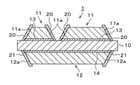
- the insulating substrate 1 is one main surface (surface) of a (plate-shaped) ceramic substrate 10 composed of AlN, Al 2 O 3 , Si 3 N 4, and the like.
- Insulating substrate 1 in which one main surface (surface) of the heat-dissipating side metal plate 12 (made of copper, aluminum, etc.) is brazed via a brazing material layer 14, the ceramic substrate 10 and the heat-dissipating side.
- a Ni plating layer 21 is provided to cover (the end portion) of the brazing material layer 14 exposed from between the metal plate 12, and at least a part of the other main surface of the heat dissipation side metal plate 12 is covered with the Ni plating layer.
- the feature is that the surface of the heat-dissipating metal plate is exposed. Further, a part or all of the side surface 12a of the heat radiating side metal plate 12 may be covered with the Ni plating layer 21, and the periphery of the other main surface (surface) of the heat radiating side metal plate 12 may be covered with the Ni plating. It may be covered with layer 21.
- one main surface (surface) of the circuit-side metal plate 11 (made of copper, aluminum, etc.) is brazed to the other main surface (surface) of the ceramic substrate 10 via the brazing material layer 13. .
- the heat radiation side metal plate 12 is a copper plate or a copper alloy plate
- the circuit side metal plate 11 is a copper plate or a copper alloy plate.
- the region where the other main surface of the heat radiating side metal plate 12 is not covered with the Ni plating layer and the main surface of the heat radiating side metal plate is exposed is the other main surface of the heat radiating side metal plate. It is preferably 70 area% or more, more preferably 80% or more, and further preferably 90% or more with respect to the surface area.
- one main surface (surface) of the circuit-side metal plate 11 is brazed to the other main surface (upper surface) of the ceramic substrate 10 by a brazing material layer 13, and one of the ceramic substrates 10 is brazed.
- a state in which one main surface (surface) of the heat radiation side metal plate 12 is brazed to the main surface (lower surface) by the brazing material layer 14 is shown.
- the circuit-side metal plate 11 has a predetermined circuit shape, and an electronic component (not shown) such as a semiconductor chip is soldered to the circuit-side metal plate 11. Further, a Cu or Al heat dissipation plate (base plate, not shown) having excellent thermal conductivity is soldered to substantially the entire surface of the other surface of the heat dissipation side metal plate 12 to the power module. Etc. are produced.
- the insulating substrate 1 When the insulating substrate 1 is used as a power module, when the above-mentioned semiconductor chip is soldered to the circuit-side copper plate 11, when the heat-dissipating plate is soldered to the heat-dissipating metal plate 12, and further, the semiconductor. Due to repeated heat generation when the chip is energized, the thermal stress generated by the difference in thermal expansion rate between the ceramic substrate 10, the circuit-side metal plate 11 and the heat-dissipating metal plate 12, and the heat cycle load, the circuit-side metal plate 11. At the end of the heat-dissipating side metal plate 12, stress concentration may occur on the surface of the ceramic substrate 10 to cause cracks in the ceramic substrate 10.
- the circuit-side metal plate 11 and the heat-dissipating side are formed by forming the side surfaces 11a and 12a of the circuit-side metal plate 11 and the heat-dissipating-side metal plate 12 on the tapered surface.
- measures are taken to alleviate the stress concentration generated on the ceramic substrate 10.
- a technique for improving heat cycle characteristics by forming a step at the end of a copper plate is also known. Whether or not cracks can be prevented in the ceramic substrate 10 of the insulating substrate 1 against such thermal stress and heat cycle load can be evaluated by the furnace resistance of the insulating substrate 1 (single unit) described later.
- the insulating substrate 1 had a problem even if the above-mentioned furnace resistance was satisfied. That is, in a state where the heat radiating plate is soldered (for example, in a state of being incorporated in a semiconductor power module), a crack may occur in the ceramic substrate 10 at a portion (joint region) inside the end portion of the heat radiating side metal plate 12. I found that. The present inventor investigated the cause of cracks generated in the ceramic substrate 10 at a portion inside the end portion of the heat-dissipating side metal plate 12.
- the heat radiating plate is soldered to the heat radiating side metal plate 12
- the components constituting the solder for example, Sn
- solder erosion of the brazing filler metal layer 14 occurs, such as formation of compounds with elements such as Ag and Cu.
- cracks which are considered to be caused by the formation of a brittle compound such as Cu—Sn in the brazing filler metal layer 14 due to the solder biting of the brazing filler metal layer 14, are formed inside the brazing filler metal layer 14 (substantially parallel to the bonding interface). It was observed to occur (in the direction).
- the ceramic substrate was found at a portion in the brazing filler metal layer 14 inside the end portion of the heat radiation side metal plate 12 and at the tip portion of a crack in the brazing filler metal layer 14. It was observed that cracks were generated in the thickness direction from one surface (surface) of 10. Further, when stress analysis was performed by simulation, it was confirmed that when the cracks were present in the brazing filler metal layer 14, stress concentration was generated on the surface of the ceramic substrate 10 at the tip of the cracks, and the stress concentration caused the ceramics. It was found that cracks were generated on the surface of the substrate 10.
- the operating temperature of power modules has tended to rise, and the use of high-temperature solder having a high Sn content has increased, resulting in an increase in the occurrence of cracks in the ceramic substrate 10 due to the above-mentioned corrosion of the brazing material.
- the solder by preventing the solder from coming into contact with the brazing filler metal layer 14 by Ni plating, erosion of Sn or the like into the brazing filler metal layer 14 is avoided, and cracks in the brazing filler metal layer 14 are prevented.
- the Ni plating layer 21 is provided so as to cover the end portion of the brazing material layer 14 exposed from between the ceramic substrate 10 and the heat radiation side metal plate 12.
- the end portion of the brazing material layer 14 exposed from between the ceramic substrate 10 and the heat radiating side metal plate 12 and a part of the side surface 12a of the heat radiating side metal plate 12 are covered so as to cover a part of the side surface 12a of the heat radiating side metal plate 12.
- the Ni plating layer 21 is provided.
- the heat-dissipating side metal plate 12 On the surface of the heat-dissipating side metal plate 12 excluding the joint surface (one surface) with the ceramic substrate 10, the heat-dissipating side metal plate 12 is exposed in the remaining portion where the Ni plating layer 21 does not exist. That is, there is no Ni plating layer 21 on the other surface of the heat radiating plate side metal plate 12 (lower surface in FIG. 1) and the portion excluding a part of the side surface 12a of the heat radiating side metal plate 12, and the surface of the heat radiating side metal plate 12 is not provided. Is exposed.
- a Ni plating region is provided in which a Ni plating layer 21 is formed to cover the brazing material layer 14 exposed from between the ceramic substrate 10 and the heat radiation side metal plate 12, and the other main surface of the heat radiation side metal plate 12 is provided.
- a region excluding at least the periphery thereof is an insulating substrate 1 which is a non-Ni plated region in which Ni plating is not formed. If the entire surface of the heat radiating side metal plate 12 is covered with Ni plating, the resistance to passing through the furnace may deteriorate. Therefore, it is preferable not to cover the other main surface of the heat radiating side metal plate 12 with Ni plating.
- the Ni-plated layer 21 may have a function of preventing mutual diffusion between the components (for example, Ag) in the brazing material layer and the solder constituents (for example, Sn) from the brazing material layer 14, and the present invention may be used.
- the Ni plating layer means a Ni plating layer or a Ni alloy plating layer, and also includes Ni or Ni alloy plating such as an electric Ni plating layer, a non-electrolytic Ni-P plating layer, and a non-electrolytic Ni-B plating layer.
- a Ni plating layer 20 may be provided so as to cover the end portion of the brazing material layer 13 exposed from between the ceramic substrate 10 and the circuit side metal plate 11.
- the brazing material layer 13 (end portion) exposed from between the ceramic substrate 10 and the circuit-side metal plate 11 and a part of the side surface 11a of the circuit-side metal plate 11 are covered.
- the surface of the circuit-side metal plate 11 is exposed in the remaining portion not covered by the Ni plating layer 20, that is, the circuit.
- an electronic component such as a semiconductor chip is mounted on the other surface of the circuit-side metal plate 11 having a predetermined circuit shape by soldering or the like. Will be done. Further, a Cu or Al heat radiating plate (base plate, not shown) having excellent thermal conductivity is soldered to the other surface of the heat radiating side metal plate 12. As a result, a semiconductor power module or the like is manufactured.
- the end portion of the brazing material layer 13 exposed from between the ceramic substrate 10 and the circuit side metal plate 11 is a Ni plating layer 20. It is covered.
- the brazing filler metal layer 13 on the circuit side does not have to be coated with Ni plating. This is because, when an electronic component is soldered to the circuit-side metal plate 11 in the process of assembling the power module, it is usually unlikely that the solder will adhere to the circuit-side brazing filler metal layer 13.
- electroless plating immersion plating
- plating resist is applied to the other main surface (surface) of the circuit-side metal plate 11 and the other main surface (surface) of the heat-dissipating metal plate 12 so that Ni plating is not coated, and then nickel-free Ni plating is applied. Since each surface is not covered with Ni plating, the characteristics such as furnace resistance and ultrasonic bondability of terminals are good.
- the brazing material layer 13 on the circuit side is also coated with Ni plating.
- Ni plating has higher hardness than the circuit side metal plate 11 such as copper and aluminum and the heat radiation side metal plate 12, and further has higher hardness due to the thermal history such as soldering of chips and heat radiation plates like electroless Ni-P plating. May become.
- Ni plating with high hardness deteriorates the resistance to passing through the furnace, but according to the present invention, in a structure in which the entire metal plate of the insulating substrate (the other main surface of the circuit side metal plate and the heat radiation side metal plate) is covered with Ni plating. Therefore, there is no problem of deterioration of furnace resistance due to Ni plating having high hardness.
- the Ni plating layer does not exist on the surface where the copper bus bar and the circuit upper surface of the insulating substrate are joined, the copper of the copper bus bar and the copper of the circuit are bonded at the time of ultrasonic joining of the copper bus bar. Solid phase diffusion is promoted, and terminal bonding with high bonding strength can be obtained.
- the power module is excellent in mountability (further resistance and ultrasonic bonding property) at the time of assembling, and at high temperature in the power module (structure in which an insulating substrate is soldered to a heat sink). It is possible to provide an insulating substrate having excellent heat cycle characteristics.
- a Ni plating layer 20 is provided so as to cover an end portion of the brazing metal layer 13 on the circuit side and a part of the side surface 11a of the metal plate 11 on the circuit side, and the end portion of the brazing filler metal layer 14 on the heat dissipation side.
- An example is shown in which the Ni plating layer 21 is provided so as to cover a part of the side surface 12a of the heat radiation side metal plate 12, but as shown in FIG. 2, in addition to the ends of the brazing filler metal layers 13 and 14, the circuit
- the entire side surfaces 11a and 12a of the side metal plate 11 and the heat radiation side metal plate 12 may be covered with the Ni plating layers 20 and 21. Further, as shown in FIG.
- one main surface of a heat-dissipating metal plate is bonded to one main surface of a ceramic substrate via a brazing filler metal layer, and the other main surface of the ceramic substrate is bonded to a circuit-side metal.
- a plating resist is formed on the other main surface of the heat-dissipating metal plate (and preferably the other main surface of the circuit-side metal plate), and the insulating substrate on which the resist is formed is immersed in a Ni plating solution.
- a Ni-plated layer is formed on the brazing filler metal layer exposed from between the ceramic substrate on which the resist is not formed and the heat-dissipating metal plate (and preferably between the ceramic substrate and the circuit-side metal plate), and then a Ni-plated layer is formed. It is characterized by peeling off the resist. A part or all of the side surface of the heat radiation side metal plate and the circuit side metal plate may be covered with the Ni plating layer, and the periphery of the other main surface of the heat radiation side metal plate is covered with the Ni plating layer. It may be broken.
- the heat dissipation side metal plate and the circuit side metal plate are preferably copper plates or copper alloy plates, and the brazing metal layer is composed of any one metal component selected from Cu, Ag, and Sn, and Ti, Hf, and Zr. It is preferable to have any one of the active metal components selected from the above.
- an ultraviolet curable alkaline stripping resist having a predetermined circuit pattern shape is applied by screen printing to the other main surface (the surface opposite to the surface bonded to the ceramic substrate) of the copper plate for forming the circuit pattern of the bonded body.
- a 45 mm ⁇ 47 mm rectangular UV-curable alkali peeling resist is placed in the center of the other main surface (the surface opposite to the surface bonded to the ceramic substrate) of the copper plate for forming the heat-dissipating side copper plate of the bonded body.
- the unnecessary part of the copper plate is etched with an etching solution consisting of copper chloride, hydrochloric acid and the rest of the water, and the resist is made with an aqueous sodium hydroxide solution. It was removed to form a circuit pattern (circuit-side copper plate) and a heat-dissipating-side copper plate made of copper plates.
- the intermediate product was immersed in a chemical polishing solution consisting of 14% by mass of sulfuric acid, 3.2% by mass of hydrogen, and the remaining water at 45 ° C. for 5 minutes, and the surfaces of the circuit-side copper plate and the heat-dissipating-side copper plate were immersed. Is removed by chemical polishing so that the active metal-containing brazing material protrudes from the side surfaces of the circuit-side copper plate and the heat-dissipating side copper plate by about 0.3 mm, and the process of forming the circuit-side copper plate and the heat-dissipating side copper plate having a predetermined shape is completed. rice field.
- an ultraviolet curable alkali peeling resist is applied by screen printing on the entire surface of the main surface of the circuit side copper plate and the heat radiation side copper plate, and the resist is irradiated with ultraviolet rays to be cured. Only the main surface of each copper plate was covered with a resist film.
- electroless Ni-P plating is applied to the bonded body with a resist film to form a plating film having a thickness of 4 ⁇ m, and then the resist is removed with an aqueous sodium hydroxide solution between the ceramic substrate and the heat-dissipating copper plate.
- a metal-ceramic insulating substrate was obtained in which the brazing filler metal layer exposed from the above, the brazing filler metal layer exposed from between the ceramic substrate and the circuit side copper plate, and the side surfaces of each copper plate were coated with a Ni plating layer.
- the Ni plating layer is not formed on the other main surfaces of the circuit-side metal plate and the heat-dissipating-side metal plate.
- the above-mentioned metal on the paste solder - that mounting the ceramic insulating substrate after heating to 270 ° C. under a N 2 atmosphere, the temperature is lowered after performing the evacuation while maintaining a 270 ° C. 3 min Then, the metal-ceramic insulating substrate was soldered to the copper base plate (heat dissipation plate).
- the solder thickness after soldering was about 200 ⁇ m.
- Comparative Example 1 As shown in FIG. 4, the resist printing step (for partial Ni plating) and the electroless Ni-P plating step after forming the circuit side copper plate and the heat dissipation side copper plate are not performed, and no Ni plating layer is present.
- a metal-ceramics insulating substrate of Comparative Example 1 was obtained by the same method as in Example 1 except for the above.
- the metal-ceramic insulating substrate of Comparative Example 1 had a bonding area ratio of 70% or more and a share strength of 1500 N or more at the ultrasonic bonding portion, and showed good ultrasonic bonding properties. Further, when the cross section of the ultrasonic bonding portion was observed by SEM / EDS, it was confirmed that the copper terminal portion and the copper circuit portion of the insulating substrate were integrated.
- Comparative Example 2 As shown in FIG. 5, the surface of the circuit-side copper plate and the heat-dissipating copper plate of the insulating substrate has a thickness of 4 ⁇ m without performing the resist printing step (for partial Ni plating) after forming the circuit-side copper plate and the heat-dissipating side copper plate.
- a metal-ceramic insulating substrate of Comparative Example 2 was obtained by the same method as in Example 1 except that it was covered with a Ni-P plating layer.
- the bonding area ratio of the ultrasonic bonding portion was 50%, the share strength was as low as 600N, and the ultrasonic bonding property was poor.
- SEM / EDS observation was performed on the cross section of the ultrasonic joint, there was a place where a Ni-P plating film remained between the copper terminal and the copper circuit of the insulating substrate, and the copper terminal and copper were found. The circuit part was not integrated.
- Example 1 The results of Example 1 and Comparative Examples 1 and 2 are summarized in Table 1.
- the Ni-plated layer When a Ni-plated layer is formed on the entire surface of the circuit-side metal plate (circuit-side copper plate) and the heat-dissipating-side metal plate (heat-dissipating-side copper plate) of the insulating substrate, the Ni-plated layer contains Ag of the brazing material layer and Sn derived from solder. In order to prevent mutual diffusion, the above-mentioned brazing metal is not eaten. However, when a Ni-plated layer is formed on the entire surface of the circuit-side metal plate (circuit-side copper plate) and the heat-dissipating-side metal plate (heat-dissipating-side copper plate) of the insulating substrate, the presence of the hard Ni-plated layer causes power.
- the present invention can be used for an insulating substrate used for, for example, a semiconductor power module.
- Insulation board 10 Ceramic board 11 Circuit side metal plate (circuit side copper plate) 12 Heat dissipation side metal plate (heat dissipation side copper plate) 13, 14 Wax layer 11a, 12a Side surface 20, 21 Ni plating layer
Abstract
L'invention concerne un substrat d'isolation (1) dans lequel une des faces principales d'une plaque métallique côté dissipation de chaleur (12) est brasée sur une des faces principales d'un substrat en céramique (10) par l'intermédiaire d'une couche de brasure (14). Ce substrat d'isolation (1) est caractéristique en ce qu'une couche de placage de Ni (20) revêtant la couche de brasure (14) exposée entre le substrat en céramique (10) et la plaque métallique côté dissipation de chaleur (12), est agencée, au moins une partie de l'autre face principale de la plaque métallique côté dissipation de chaleur (12) n'est pas revêtue par la couche de placage de Ni (20), et la surface de la plaque métallique côté dissipation de chaleur (12) se trouve dans un état d'exposition. Le substrat d'isolation (1) (corps simple) présente une excellente résistance au passage au four. En outre, l'invention permet d'obtenir un substrat d'isolation (1) également excellent en termes de caractéristiques de cycle de traitement thermique dans un état dans lequel une plaque de dissipation de chaleur est soudée sur le substrat d'isolation (1).
Priority Applications (4)
| Application Number | Priority Date | Filing Date | Title |
|---|---|---|---|
| CN202180049035.2A CN115812342A (zh) | 2020-07-15 | 2021-06-29 | 绝缘基板及其制造方法 |
| KR1020237001568A KR20230039649A (ko) | 2020-07-15 | 2021-06-29 | 절연 기판 및 그 제조 방법 |
| EP21842920.7A EP4184562A1 (fr) | 2020-07-15 | 2021-06-29 | Substrat d'isolation, et procédé de fabrication de celui-ci |
| US18/010,104 US20230268245A1 (en) | 2020-07-15 | 2021-06-29 | Insulating substrate and manufacturing method thereof |
Applications Claiming Priority (2)
| Application Number | Priority Date | Filing Date | Title |
|---|---|---|---|
| JP2020-121493 | 2020-07-15 | ||
| JP2020121493A JP2022024310A (ja) | 2020-07-15 | 2020-07-15 | 絶縁基板およびその製造方法 |
Publications (1)
| Publication Number | Publication Date |
|---|---|
| WO2022014319A1 true WO2022014319A1 (fr) | 2022-01-20 |
Family
ID=79555435
Family Applications (1)
| Application Number | Title | Priority Date | Filing Date |
|---|---|---|---|
| PCT/JP2021/024584 WO2022014319A1 (fr) | 2020-07-15 | 2021-06-29 | Substrat d'isolation, et procédé de fabrication de celui-ci |
Country Status (6)
| Country | Link |
|---|---|
| US (1) | US20230268245A1 (fr) |
| EP (1) | EP4184562A1 (fr) |
| JP (1) | JP2022024310A (fr) |
| KR (1) | KR20230039649A (fr) |
| CN (1) | CN115812342A (fr) |
| WO (1) | WO2022014319A1 (fr) |
Citations (8)
| Publication number | Priority date | Publication date | Assignee | Title |
|---|---|---|---|---|
| JP2001024296A (ja) | 1999-07-07 | 2001-01-26 | Kyocera Corp | セラミック回路基板 |
| JP2002009212A (ja) * | 2000-06-23 | 2002-01-11 | Denki Kagaku Kogyo Kk | 放熱構造体の製造方法 |
| JP2006228918A (ja) * | 2005-02-17 | 2006-08-31 | Hitachi Metals Ltd | セラミックス回路基板およびそれを用いた半導体モジュール |
| JP2009070863A (ja) | 2007-09-11 | 2009-04-02 | Hitachi Ltd | 半導体パワーモジュール |
| JP2010241627A (ja) | 2009-04-03 | 2010-10-28 | Dowa Metaltech Kk | 金属−セラミックス接合基板およびそれに用いるろう材 |
| JP2011097049A (ja) * | 2009-10-01 | 2011-05-12 | Hitachi Metals Ltd | 窒化珪素回路基板およびその製造方法 |
| JP2011181634A (ja) * | 2010-02-26 | 2011-09-15 | Nisshin Steel Co Ltd | 半導体発熱部品搭載用放熱構造体の製造法 |
| JP2016076603A (ja) * | 2014-10-07 | 2016-05-12 | Dowaメタルテック株式会社 | 金属−セラミックス回路基板およびその製造方法 |
-
2020
- 2020-07-15 JP JP2020121493A patent/JP2022024310A/ja active Pending
-
2021
- 2021-06-29 WO PCT/JP2021/024584 patent/WO2022014319A1/fr unknown
- 2021-06-29 CN CN202180049035.2A patent/CN115812342A/zh active Pending
- 2021-06-29 EP EP21842920.7A patent/EP4184562A1/fr active Pending
- 2021-06-29 US US18/010,104 patent/US20230268245A1/en active Pending
- 2021-06-29 KR KR1020237001568A patent/KR20230039649A/ko unknown
Patent Citations (8)
| Publication number | Priority date | Publication date | Assignee | Title |
|---|---|---|---|---|
| JP2001024296A (ja) | 1999-07-07 | 2001-01-26 | Kyocera Corp | セラミック回路基板 |
| JP2002009212A (ja) * | 2000-06-23 | 2002-01-11 | Denki Kagaku Kogyo Kk | 放熱構造体の製造方法 |
| JP2006228918A (ja) * | 2005-02-17 | 2006-08-31 | Hitachi Metals Ltd | セラミックス回路基板およびそれを用いた半導体モジュール |
| JP2009070863A (ja) | 2007-09-11 | 2009-04-02 | Hitachi Ltd | 半導体パワーモジュール |
| JP2010241627A (ja) | 2009-04-03 | 2010-10-28 | Dowa Metaltech Kk | 金属−セラミックス接合基板およびそれに用いるろう材 |
| JP2011097049A (ja) * | 2009-10-01 | 2011-05-12 | Hitachi Metals Ltd | 窒化珪素回路基板およびその製造方法 |
| JP2011181634A (ja) * | 2010-02-26 | 2011-09-15 | Nisshin Steel Co Ltd | 半導体発熱部品搭載用放熱構造体の製造法 |
| JP2016076603A (ja) * | 2014-10-07 | 2016-05-12 | Dowaメタルテック株式会社 | 金属−セラミックス回路基板およびその製造方法 |
Also Published As
| Publication number | Publication date |
|---|---|
| JP2022024310A (ja) | 2022-02-09 |
| KR20230039649A (ko) | 2023-03-21 |
| CN115812342A (zh) | 2023-03-17 |
| US20230268245A1 (en) | 2023-08-24 |
| EP4184562A1 (fr) | 2023-05-24 |
Similar Documents
| Publication | Publication Date | Title |
|---|---|---|
| JP5656962B2 (ja) | 電子部品モジュール | |
| EP2980843B1 (fr) | Module d'alimentation | |
| KR20170044105A (ko) | 접합체, 히트 싱크가 부착된 파워 모듈용 기판, 히트 싱크, 접합체의 제조 방법, 히트 싱크가 부착된 파워 모듈용 기판의 제조 방법, 및 히트 싱크의 제조 방법 | |
| KR20170046649A (ko) | 접합체, 히트 싱크가 부착된 파워 모듈용 기판, 히트 싱크, 접합체의 제조 방법, 히트 싱크가 부착된 파워 모듈용 기판의 제조 방법, 및 히트 싱크의 제조 방법 | |
| JP2000323618A (ja) | 銅回路接合基板及びその製造方法 | |
| JP2002043482A (ja) | 電子回路用部材及びその製造方法並びに電子部品 | |
| JP4703377B2 (ja) | 段差回路基板、その製造方法およびそれを用いた電力制御部品。 | |
| JP4360847B2 (ja) | セラミック回路基板、放熱モジュール、および半導体装置 | |
| JP4104429B2 (ja) | モジュール構造体とそれを用いたモジュール | |
| US10798824B2 (en) | Method for manufacturing insulated circuit board, insulated circuit board, and thermoelectric conversion module | |
| WO2022014319A1 (fr) | Substrat d'isolation, et procédé de fabrication de celui-ci | |
| JP2013191640A (ja) | パワーモジュール用基板及びその製造方法 | |
| JP2005347767A (ja) | セラミックス回路基板の製造方法 | |
| JP4018264B2 (ja) | アルミニウム−窒化アルミニウム絶縁基板の製造方法 | |
| WO2020218193A1 (fr) | Substrat de circuit céramique et module de composant électronique | |
| TWI231019B (en) | Lead frame and manufacturing method thereof and a semiconductor device | |
| WO2022014318A1 (fr) | Substrat d'isolation, et procédé de fabrication de celui-ci | |
| JP7298988B2 (ja) | セラミックス回路基板及びその製造方法 | |
| JP3199028B2 (ja) | 半導体装置及びその製造方法 | |
| JP2006279035A (ja) | セラミックス回路基板及びその製造方法 | |
| JP2001135902A (ja) | セラミックス回路基板 | |
| JP2005285885A (ja) | 半導体装置 | |
| JP2004080060A (ja) | 電子部品用パッケージ及びその製造方法 | |
| JPS628532A (ja) | 金メツキされた電子部品パツケ−ジ | |
| JP3526711B2 (ja) | 窒化アルミニウム回路基板 |
Legal Events
| Date | Code | Title | Description |
|---|---|---|---|
| 121 | Ep: the epo has been informed by wipo that ep was designated in this application |
Ref document number: 21842920 Country of ref document: EP Kind code of ref document: A1 |
|
| NENP | Non-entry into the national phase |
Ref country code: DE |
|
| ENP | Entry into the national phase |
Ref document number: 2021842920 Country of ref document: EP Effective date: 20230215 |