WO2022009259A1 - 光受信モジュール - Google Patents
光受信モジュール Download PDFInfo
- Publication number
- WO2022009259A1 WO2022009259A1 PCT/JP2020/026367 JP2020026367W WO2022009259A1 WO 2022009259 A1 WO2022009259 A1 WO 2022009259A1 JP 2020026367 W JP2020026367 W JP 2020026367W WO 2022009259 A1 WO2022009259 A1 WO 2022009259A1
- Authority
- WO
- WIPO (PCT)
- Prior art keywords
- transmission line
- block
- relay board
- receiving module
- type light
- Prior art date
- Legal status (The legal status is an assumption and is not a legal conclusion. Google has not performed a legal analysis and makes no representation as to the accuracy of the status listed.)
- Ceased
Links
Images





Classifications
-
- G—PHYSICS
- G01—MEASURING; TESTING
- G01J—MEASUREMENT OF INTENSITY, VELOCITY, SPECTRAL CONTENT, POLARISATION, PHASE OR PULSE CHARACTERISTICS OF INFRARED, VISIBLE OR ULTRAVIOLET LIGHT; COLORIMETRY; RADIATION PYROMETRY
- G01J1/00—Photometry, e.g. photographic exposure meter
- G01J1/02—Details
- G01J1/0271—Housings; Attachments or accessories for photometers
-
- G—PHYSICS
- G01—MEASURING; TESTING
- G01J—MEASUREMENT OF INTENSITY, VELOCITY, SPECTRAL CONTENT, POLARISATION, PHASE OR PULSE CHARACTERISTICS OF INFRARED, VISIBLE OR ULTRAVIOLET LIGHT; COLORIMETRY; RADIATION PYROMETRY
- G01J1/00—Photometry, e.g. photographic exposure meter
- G01J1/02—Details
- G01J1/04—Optical or mechanical part supplementary adjustable parts
- G01J1/0407—Optical elements not provided otherwise, e.g. manifolds, windows, holograms, gratings
-
- G—PHYSICS
- G01—MEASURING; TESTING
- G01J—MEASUREMENT OF INTENSITY, VELOCITY, SPECTRAL CONTENT, POLARISATION, PHASE OR PULSE CHARACTERISTICS OF INFRARED, VISIBLE OR ULTRAVIOLET LIGHT; COLORIMETRY; RADIATION PYROMETRY
- G01J1/00—Photometry, e.g. photographic exposure meter
- G01J1/42—Photometry, e.g. photographic exposure meter using electric radiation detectors
- G01J1/44—Electric circuits
- G01J1/46—Electric circuits using a capacitor
-
- H—ELECTRICITY
- H01—ELECTRIC ELEMENTS
- H01P—WAVEGUIDES; RESONATORS, LINES, OR OTHER DEVICES OF THE WAVEGUIDE TYPE
- H01P3/00—Waveguides; Transmission lines of the waveguide type
- H01P3/02—Waveguides; Transmission lines of the waveguide type with two longitudinal conductors
- H01P3/08—Microstrips; Strip lines
- H01P3/081—Microstriplines
-
- H—ELECTRICITY
- H10—SEMICONDUCTOR DEVICES; ELECTRIC SOLID-STATE DEVICES NOT OTHERWISE PROVIDED FOR
- H10F—INORGANIC SEMICONDUCTOR DEVICES SENSITIVE TO INFRARED RADIATION, LIGHT, ELECTROMAGNETIC RADIATION OF SHORTER WAVELENGTH OR CORPUSCULAR RADIATION
- H10F30/00—Individual radiation-sensitive semiconductor devices in which radiation controls the flow of current through the devices, e.g. photodetectors
- H10F30/20—Individual radiation-sensitive semiconductor devices in which radiation controls the flow of current through the devices, e.g. photodetectors the devices having potential barriers, e.g. phototransistors
- H10F30/21—Individual radiation-sensitive semiconductor devices in which radiation controls the flow of current through the devices, e.g. photodetectors the devices having potential barriers, e.g. phototransistors the devices being sensitive to infrared, visible or ultraviolet radiation
- H10F30/22—Individual radiation-sensitive semiconductor devices in which radiation controls the flow of current through the devices, e.g. photodetectors the devices having potential barriers, e.g. phototransistors the devices being sensitive to infrared, visible or ultraviolet radiation the devices having only one potential barrier, e.g. photodiodes
-
- H—ELECTRICITY
- H10—SEMICONDUCTOR DEVICES; ELECTRIC SOLID-STATE DEVICES NOT OTHERWISE PROVIDED FOR
- H10F—INORGANIC SEMICONDUCTOR DEVICES SENSITIVE TO INFRARED RADIATION, LIGHT, ELECTROMAGNETIC RADIATION OF SHORTER WAVELENGTH OR CORPUSCULAR RADIATION
- H10F30/00—Individual radiation-sensitive semiconductor devices in which radiation controls the flow of current through the devices, e.g. photodetectors
- H10F30/20—Individual radiation-sensitive semiconductor devices in which radiation controls the flow of current through the devices, e.g. photodetectors the devices having potential barriers, e.g. phototransistors
- H10F30/21—Individual radiation-sensitive semiconductor devices in which radiation controls the flow of current through the devices, e.g. photodetectors the devices having potential barriers, e.g. phototransistors the devices being sensitive to infrared, visible or ultraviolet radiation
- H10F30/22—Individual radiation-sensitive semiconductor devices in which radiation controls the flow of current through the devices, e.g. photodetectors the devices having potential barriers, e.g. phototransistors the devices being sensitive to infrared, visible or ultraviolet radiation the devices having only one potential barrier, e.g. photodiodes
- H10F30/225—Individual radiation-sensitive semiconductor devices in which radiation controls the flow of current through the devices, e.g. photodetectors the devices having potential barriers, e.g. phototransistors the devices being sensitive to infrared, visible or ultraviolet radiation the devices having only one potential barrier, e.g. photodiodes the potential barrier working in avalanche mode, e.g. avalanche photodiodes
-
- H—ELECTRICITY
- H10—SEMICONDUCTOR DEVICES; ELECTRIC SOLID-STATE DEVICES NOT OTHERWISE PROVIDED FOR
- H10F—INORGANIC SEMICONDUCTOR DEVICES SENSITIVE TO INFRARED RADIATION, LIGHT, ELECTROMAGNETIC RADIATION OF SHORTER WAVELENGTH OR CORPUSCULAR RADIATION
- H10F77/00—Constructional details of devices covered by this subclass
- H10F77/40—Optical elements or arrangements
- H10F77/407—Optical elements or arrangements indirectly associated with the devices
-
- H—ELECTRICITY
- H10—SEMICONDUCTOR DEVICES; ELECTRIC SOLID-STATE DEVICES NOT OTHERWISE PROVIDED FOR
- H10F—INORGANIC SEMICONDUCTOR DEVICES SENSITIVE TO INFRARED RADIATION, LIGHT, ELECTROMAGNETIC RADIATION OF SHORTER WAVELENGTH OR CORPUSCULAR RADIATION
- H10F77/00—Constructional details of devices covered by this subclass
- H10F77/50—Encapsulations or containers
-
- H—ELECTRICITY
- H10—SEMICONDUCTOR DEVICES; ELECTRIC SOLID-STATE DEVICES NOT OTHERWISE PROVIDED FOR
- H10F—INORGANIC SEMICONDUCTOR DEVICES SENSITIVE TO INFRARED RADIATION, LIGHT, ELECTROMAGNETIC RADIATION OF SHORTER WAVELENGTH OR CORPUSCULAR RADIATION
- H10F77/00—Constructional details of devices covered by this subclass
- H10F77/93—Interconnections
- H10F77/933—Interconnections for devices having potential barriers
-
- H—ELECTRICITY
- H10—SEMICONDUCTOR DEVICES; ELECTRIC SOLID-STATE DEVICES NOT OTHERWISE PROVIDED FOR
- H10F—INORGANIC SEMICONDUCTOR DEVICES SENSITIVE TO INFRARED RADIATION, LIGHT, ELECTROMAGNETIC RADIATION OF SHORTER WAVELENGTH OR CORPUSCULAR RADIATION
- H10F77/00—Constructional details of devices covered by this subclass
- H10F77/95—Circuit arrangements
- H10F77/953—Circuit arrangements for devices having potential barriers
-
- H—ELECTRICITY
- H10—SEMICONDUCTOR DEVICES; ELECTRIC SOLID-STATE DEVICES NOT OTHERWISE PROVIDED FOR
- H10W—GENERIC PACKAGES, INTERCONNECTIONS, CONNECTORS OR OTHER CONSTRUCTIONAL DETAILS OF DEVICES COVERED BY CLASS H10
- H10W44/00—Electrical arrangements for controlling or matching impedance
- H10W44/20—Electrical arrangements for controlling or matching impedance at high-frequency [HF] or radio frequency [RF]
-
- H—ELECTRICITY
- H10—SEMICONDUCTOR DEVICES; ELECTRIC SOLID-STATE DEVICES NOT OTHERWISE PROVIDED FOR
- H10W—GENERIC PACKAGES, INTERCONNECTIONS, CONNECTORS OR OTHER CONSTRUCTIONAL DETAILS OF DEVICES COVERED BY CLASS H10
- H10W44/00—Electrical arrangements for controlling or matching impedance
- H10W44/20—Electrical arrangements for controlling or matching impedance at high-frequency [HF] or radio frequency [RF]
- H10W44/203—Electrical connections
- H10W44/206—Wires
-
- H—ELECTRICITY
- H10—SEMICONDUCTOR DEVICES; ELECTRIC SOLID-STATE DEVICES NOT OTHERWISE PROVIDED FOR
- H10W—GENERIC PACKAGES, INTERCONNECTIONS, CONNECTORS OR OTHER CONSTRUCTIONAL DETAILS OF DEVICES COVERED BY CLASS H10
- H10W44/00—Electrical arrangements for controlling or matching impedance
- H10W44/20—Electrical arrangements for controlling or matching impedance at high-frequency [HF] or radio frequency [RF]
- H10W44/203—Electrical connections
- H10W44/216—Waveguides, e.g. strip lines
Definitions
- This disclosure relates to an optical receiving module.
- the waveguide type light receiving element is an end face incident type light receiving element that can achieve both high sensitivity and a wide band.
- An optical receiving module in which such an end face incident type light receiving element is mounted in a small and inexpensive CAN package has been proposed (see, for example, Patent Document 1).
- the present disclosure has been made to solve the above-mentioned problems, and the purpose of the present disclosure is to obtain an optical receiving module that can be miniaturized while preventing band deterioration.
- the optical receiving module includes a circular stem, a plurality of lead pins penetrating the stem and having signal lead pins, a block provided on the upper surface of the stem, and a guide provided on a side surface of the block.
- a waveguide type light receiving element an amplifier provided on the side surface of the block and amplifying an electric signal output from the waveguide type light receiving element, and an amplifier provided on the upper surface of the stem of the block and the signal lead pin.
- a first wire arranged between the first relay board, the first transmission line provided on the first relay board, one end of the first transmission line, and the output terminal of the amplifier. And a second wire connecting the other end of the first transmission line and the signal lead pin.
- the relay board on the upper surface of the stem, the degree of freedom in arranging the plurality of lead pins is increased, and the plurality of lead pins can be arranged so that the radius of the circular stem becomes smaller. Further, by using the relay board, the length of the wire between the amplifier and the signal lead pin is shortened, and the inductance of the wire is reduced. As a result, it is possible to obtain an optical receiving module that can be miniaturized while preventing deterioration of the band.
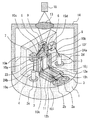
- FIG. It is a perspective view which shows the optical receiving module which concerns on Embodiment 1.
- FIG. It is a circuit diagram of the optical reception module which concerns on Embodiment 1.
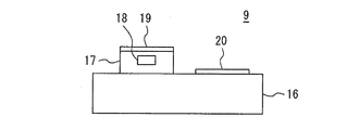
- FIG. It is sectional drawing which shows the waveguide type light receiving element.
- It is a top view which shows the optical receiving module which concerns on a comparative example.
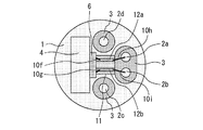
- It is a top view which shows the optical receiving module which concerns on Embodiment 1.
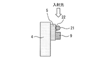
- FIG. It is an enlarged side view which shows the modification of the optical receiving module which concerns on Embodiment 1.
- FIG. It is an enlarged side view which shows the modification of the optical receiving module which concerns on Embodiment 1.
- FIG. It is a perspective view which shows the optical receiving module which concerns on Embodiment 2.
- FIG. It is a perspective view which shows the optical receiving module which concerns on Embodiment 3.
- optical receiving module according to the embodiment will be described with reference to the drawings.
- the same or corresponding components may be designated by the same reference numerals and the description may be omitted.
- FIG. 1 is a perspective view showing an optical receiving module according to the first embodiment.
- FIG. 2 is a circuit diagram of the optical receiving module according to the first embodiment.
- the stem 1 is a circular conductor and has a ground potential.
- a block 4 is provided on the upper surface of the stem 1, and the upper surface of the stem 1 and the lower surface of the block 4 are joined to each other.
- the block 4 is a conductor and is connected to the stem 1 to have a ground potential.
- a submount 5, a TIA (Transimpedance Amplifier) 6, and capacitors 7 and 8 are provided on one side surface of the block 4.
- the waveguide type light receiving element 9 is mounted on the submount 5.
- the waveguide type light receiving element 9 is a PD (Photo Diode) or an APD (Avalanche Photo Diode). Since the plurality of configurations are provided on one side surface of the block 4 in this way, the width of the block 4 is wider than the distance between the lead pins 2c and 2d.
- the bottom electrodes of the capacitors 7 and 8 are connected to the block 4.
- the top electrodes of the capacitors 7 and 8 are connected to the lead pins 2c and 2d by wires 10a and 10b, respectively.
- the top electrode of the capacitor 7 is connected to the cathode electrode of the waveguide type light receiving element 9 by a wire 10c.
- the top electrode of the capacitor 8 is connected to the power supply terminal of the TIA 6 by the wire 10d.
- the anode electrode of the waveguide type light receiving element 9 is connected to the input terminal of the TIA 6 by the wire 10e.
- a relay board 11 made of an insulator is provided on the upper surface of the stem 1 and is arranged between the block 4 and the lead pins 2a and 2b.
- Transmission lines 12a and 12b are provided on the relay board 11. One end of the transmission line 12a is connected to the positive phase output terminal of the TIA 6 by the wire 10f. One end of the transmission line 12b is connected to the reverse phase output terminal of the TIA 6 by a wire 10g. The other ends of the transmission lines 12a and 12b are connected to the lead pins 2a and 2b by wires 10h and 10i, respectively.
- the wires 10a to 10i are, for example, Au wires.
- the cap 14 having the lens 13 is fixed to the upper surface of the stem 1 so as to cover the waveguide type light receiving element 9 and the like.
- the waveguide type light receiving element 9 is arranged so that the end face thereof is substantially perpendicular to the optical axis of the incident light from the optical fiber 15.
- the incident light from the optical fiber 15 is collected by the lens 13 and incident on the end face of the waveguide type light receiving element 9. Therefore, the waveguide type light receiving element 9 is arranged in the central portion of the circular stem 1.
- the waveguide type light receiving element 9 converts an incident optical signal into an electric signal.
- the TIA 6 is a differential amplifier that amplifies the electric signal output from the waveguide type light receiving element 9.
- the differential output signal of the TIA 6 is output to the outside of the module via the transmission lines 12a and 12b and the lead pins 2a and 2b.
- the lead pin 2c is provided to supply electric power to the waveguide type light receiving element 9.
- the lead pin 2d is provided to supply power to the TIA 6.
- FIG. 3 is a cross-sectional view showing a waveguide type light receiving element.
- a semiconductor laminated structure 17 is provided on the semiconductor substrate 16.
- the semiconductor laminated structure 17 has a waveguide 18.
- the anode electrode 19 is provided on the semiconductor laminated structure 17.
- a cathode electrode 20 is provided on the semiconductor substrate 16.
- the waveguide 18 serves as a light receiving portion of the waveguide type light receiving element 9.
- FIG. 4 is a top view showing an optical receiving module according to a comparative example.
- the relay board 11 does not exist in the comparative example. Therefore, the positive phase output terminal and the negative phase output terminal of the TIA 6 are directly connected to the lead pins 2a and 2b by the wires 10h and 10i, respectively.
- the lead pins 2a and 2b for signals are brought closer to the block 4 in order to shorten the wires 10h and 10i, a plurality of lead pins 2a to 2d are lined up in a row. Then, the lead pins 2a and 2b for signals and the lead pins 2c and 2d for power supply need to be separated from each other to some extent. Therefore, the radius of the circular stem 1 becomes large.
- FIG. 5 is a top view showing the optical receiving module according to the first embodiment.
- a relay board 11 for connecting between the TIA 6 and the lead pins 2a and 2b for signals is provided on the upper surface of the stem 1.
- the relay board 11 is arranged between the lead pins 2c and 2d for power supply.
- the relay board 11 By using the relay board 11 in this way, the degree of freedom in arranging the plurality of lead pins 2a to 2d is increased, and the plurality of lead pins 2a to 2d can be arranged so that the radius of the circular stem 1 becomes smaller.
- the relay board 11 the length of the wire between the TIA 6 and the lead pins 2a and 2b for signals is shortened, and the inductance of the wire is reduced. As a result, it is possible to obtain an optical receiving module that can be miniaturized while preventing deterioration of the band.
- FIG. 6 and 7 are enlarged side views showing a modified example of the optical receiving module according to the first embodiment.
- the lens 21 is adhered to the end surface of the waveguide type light receiving element 9 with an adhesive 22.
- the lens 21 is adhered to the submount 5 with an adhesive 22 in front of the end surface of the waveguide type light receiving element 9.
- FIG. 8 is a perspective view showing the optical receiving module according to the second embodiment.
- a relay board 23 made of an insulator is provided on the side surface of the block 4.
- Transmission lines 24a and 24b are provided on the relay board 23.
- One end of the transmission line 24a is connected to the positive phase output of the TIA 6 by a wire 10f.
- One end of the transmission line 24b is connected to the reverse phase output of the TIA 6 by a wire 10g.
- the other ends of the transmission lines 24a and 24b are connected to the transmission lines 12a and 12b by wires 10j and 10k, respectively.
- the two relay boards 11 and 23 may be integrated to form a relay board having an L-shaped cross section.
- the TIA 6 on the side surface of the block 4 and the transmission lines 12a and 12b of the relay board 11 on the upper surface of the stem 1 are connected.
- the wires 10f and 10g are lengthened, and the inductance of the wires increases.
- the wires 10f, 10g, 10j, and 10k can be shortened by using the relay board 23 also on the side surface of the block 4. As a result, the inductance can be reduced and the deterioration of the band can be suppressed.
- the wire becomes long because a space for operating the capillary is required when the TIA 6 and the relay board 11 on the orthogonal planes are connected by the wire.
- the wire can be shortened because there is a space for the capillary to operate when the wire is connected between the TIA 6 and the relay board 23 on the same plane.
- Other configurations and effects are the same as those in the first embodiment.
- the transmission lines 24a and 24b may be connected to the transmission lines 12a and 12b by soldering. As a result, the overall wire length can be shortened, so that the inductance can be further reduced.
- FIG. 9 is a perspective view showing the optical receiving module according to the third embodiment.
- the block 4 is made of an insulating material such as ceramic.
- a GND wiring pattern 25 and transmission lines 24a and 24b are provided on the surface of the block 4.
- One ends of the transmission lines 24a and 24b are connected to the positive phase output and the negative phase output of the TIA 6 by wires 10f and 10g, respectively.
- the other ends of the transmission lines 24a and 24b are joined to the transmission lines 12a and 12b by solders 26a and 26b, respectively.
- the transmission lines 24a and 24b may be connected to the transmission lines 12a and 12b by wires.
- the relay board 23 on the block 4 can be omitted by providing the transmission lines 24a and 24b on the surface of the insulating block 4.
- Other configurations and effects are the same as those in the second embodiment.
Landscapes
- Physics & Mathematics (AREA)
- General Physics & Mathematics (AREA)
- Spectroscopy & Molecular Physics (AREA)
- Engineering & Computer Science (AREA)
- Power Engineering (AREA)
- Light Receiving Elements (AREA)
- Microelectronics & Electronic Packaging (AREA)
Abstract
複数のリードピン(2a~2d)が、円形のステム(1)を貫通し、信号用リードピン(2a,2b)を有する。ブロック(4)がステム(1)の上面に設けられている。導波路型受光素子(9)がブロック(4)の側面に設けられている。増幅器(6)がブロック(4)の側面に設けられ、導波路型受光素子(9)から出力された電気信号を増幅する。第1の中継基板(11)がステム(1)の上面に設けられ、ブロック(4)と信号用リードピン(2a,2b)の間に配置されている。第1の伝送線路(12a,12b)が第1の中継基板(11)に設けられている。第1のワイヤ(10f,10g)が第1の伝送線路(12a,12b)の一端と増幅器(6)の出力端子を接続する。第2のワイヤ(10h,10i)が第1の伝送線路(12a,12b)の他端と信号用リードピン(2a,2b)を接続する。
Description
本開示は、光受信モジュールに関する。
導波路型受光素子は、高感度と広帯域を両立できる端面入射型の受光素子である。このような端面入射型の受光素子を小型・安価なCANパッケージに搭載した光受信モジュールが提案されている(例えば、特許文献1参照)。
従来のモジュールでは、ステム上のブロックの側面に設けられた増幅器と信号用のリードピンを接続するワイヤの長さが長くなり、ワイヤのインダクタンスが増加して帯域が劣化するという問題があった。
また、信号用のリードピン以外にも複数のリードピンがステムを貫通している。ワイヤを短くするために信号用のリードピンをブロックに近づけると複数のリードピンの配置の自由度が下がる。従って、円形のステムの半径が小さくなるように複数のリードピンを配置することができなくなるため、モジュールが大きくなるという問題があった。
本開示は、上述のような課題を解決するためになされたもので、その目的は帯域の劣化を防ぎつつ小型化が可能な光受信モジュールを得るものである。
本開示に係る光受信モジュールは、円形のステムと、前記ステムを貫通し、信号用リードピンを有する複数のリードピンと、前記ステムの上面に設けられたブロックと、前記ブロックの側面に設けられた導波路型受光素子と、前記ブロックの前記側面に設けられ、前記導波路型受光素子から出力された電気信号を増幅する増幅器と、前記ステムの前記上面に設けられ、前記ブロックと前記信号用リードピンの間に配置された第1の中継基板と、前記第1の中継基板に設けられた第1の伝送線路と、前記第1の伝送線路の一端と前記増幅器の出力端子を接続する第1のワイヤと、前記第1の伝送線路の他端と前記信号用リードピンを接続する第2のワイヤとを備えることを特徴とする。
本開示では、ステムの上面に中継基板を設けることで複数のリードピンの配置の自由度が上がり、円形のステムの半径が小さくなるように複数のリードピンを配置することができる。また、中継基板を用いることで増幅器と信号用リードピンとの間のワイヤの長さが短くなり、ワイヤのインダクタンスが低減する。この結果、帯域の劣化を防ぎつつ小型化が可能な光受信モジュールを得ることができる。
実施の形態に係る光受信モジュールについて図面を参照して説明する。同じ又は対応する構成要素には同じ符号を付し、説明の繰り返しを省略する場合がある。
実施の形態1.
図1は、実施の形態1に係る光受信モジュールを示す斜視図である。図2は、実施の形態1に係る光受信モジュールの回路図である。ステム1は円形の導電体であり、接地電位になっている。
図1は、実施の形態1に係る光受信モジュールを示す斜視図である。図2は、実施の形態1に係る光受信モジュールの回路図である。ステム1は円形の導電体であり、接地電位になっている。
信号用のリードピン2a,2bと電源用のリードピン2c,2dがステム1を貫通している。ステム1とリードピン2a~2dとの間に絶縁性のシールガラス3が設けられているため、両者は互いに絶縁されている。リードピン2a~2dの先端はステム1の上面から突出している。
ステム1の上面にブロック4が設けられ、ステム1の上面とブロック4の下面が接合されている。本実施の形態ではブロック4は導電体であり、ステム1に接続されて接地電位になっている。サブマウント5、TIA(Transimpedance Amplifier)6、キャパシタ7,8がブロック4の1つの側面に設けられている。導波路型受光素子9がサブマウント5に実装されている。導波路型受光素子9はPD(Photo Diode)又はAPD(Avalanche Photo Diode)である。このように複数の構成がブロック4の1つの側面に設けられるため、ブロック4の横幅はリードピン2c,2dの間隔よりも広くなる。
キャパシタ7,8の下面電極がブロック4に接続されている。キャパシタ7,8の上面電極がそれぞれリードピン2c,2dにワイヤ10a,10bにより接続されている。キャパシタ7の上面電極がワイヤ10cにより導波路型受光素子9のカソード電極に接続されている。キャパシタ8の上面電極がワイヤ10dによりTIA6の電源端子に接続されている。導波路型受光素子9のアノード電極がワイヤ10eによりTIA6の入力端子に接続されている。
絶縁体からなる中継基板11がステム1の上面に設けられ、ブロック4とリードピン2a,2bの間に配置されている。中継基板11に伝送線路12a,12bが設けられている。伝送線路12aの一端はワイヤ10fによりTIA6の正相出力端子に接続されている。伝送線路12bの一端はワイヤ10gによりTIA6の逆相出力端子に接続されている。伝送線路12a,12bの他端はそれぞれワイヤ10h,10iによりリードピン2a,2bに接続されている。ワイヤ10a~10iは例えばAuワイヤである。
レンズ13を有するキャップ14が、導波路型受光素子9等を覆うようにステム1の上面に固定されている。導波路型受光素子9は、端面が光ファイバ15からの入射光の光軸に対してほぼ垂直になるように配置されている。光ファイバ15からの入射光がレンズ13により集光され、導波路型受光素子9の端面に入射される。このため、導波路型受光素子9は円形のステム1の中央部に配置される。
導波路型受光素子9は入射した光信号を電気信号に変換する。TIA6は、導波路型受光素子9から出力された電気信号を増幅する差動増幅器である。TIA6の差動出力信号は伝送線路12a,12b及びリードピン2a,2bを介してモジュール外部に出力される。リードピン2cは導波路型受光素子9に電力を供給するために設けられている。リードピン2dはTIA6に電力を供給するために設けられている。
図3は、導波路型受光素子を示す断面図である。半導体基板16の上に半導体積層構造17が設けられている。半導体積層構造17は導波路18を有する。半導体積層構造17の上にアノード電極19が設けられている。半導体基板16の上にカソード電極20が設けられている。導波路18が導波路型受光素子9の受光部となる。
続いて、本実施の形態の効果を比較例と比較して説明する。図4は、比較例に係る光受信モジュールを示す上面図である。比較例には中継基板11が存在しない。このため、TIA6の正相出力端子と逆相出力端子がそれぞれワイヤ10h,10iにより直接的にリードピン2a,2bに接続されている。ワイヤ10h,10iを短くするために信号用のリードピン2a,2bをブロック4に近づけると、複数のリードピン2a~2dが一列に並ぶ。そして、信号用のリードピン2a,2bと電源用のリードピン2c,2dはある程度の距離を離す必要がある。このため、円形のステム1の半径が大きくなってしまう。
図5は、実施の形態1に係る光受信モジュールを示す上面図である。TIA6と信号用のリードピン2a,2bとの間を接続する中継基板11がステム1の上面に設けられている。中継基板11は電源用のリードピン2c,2dの間に配置される。このように中継基板11を用いることで複数のリードピン2a~2dの配置の自由度が上がり、円形のステム1の半径が小さくなるように複数のリードピン2a~2dを配置することができる。また、中継基板11を用いることでTIA6と信号用のリードピン2a,2bとの間のワイヤの長さが短くなり、ワイヤのインダクタンスが低減する。この結果、帯域の劣化を防ぎつつ小型化が可能な光受信モジュールを得ることができる。
図6及び図7は、実施の形態1に係る光受信モジュールの変形例を示す拡大側面図である。図6では、導波路型受光素子9の端面にレンズ21が接着剤22で接着されている。図7では、導波路型受光素子9の端面の前方において、レンズ21がサブマウント5に接着剤22で接着されている。これにより、光ファイバ15と導波路型受光素子9の光結合トレランスが広がり、実装位置精度を緩和することができる。
実施の形態2.
図8は、実施の形態2に係る光受信モジュールを示す斜視図である。絶縁体からなる中継基板23がブロック4の側面に設けられている。中継基板23に伝送線路24a,24bが設けられている。伝送線路24aの一端はワイヤ10fによりTIA6の正相出力に接続されている。伝送線路24bの一端はワイヤ10gによりTIA6の逆相出力に接続されている。伝送線路24a,24bの他端はそれぞれワイヤ10j,10kにより伝送線路12a,12bに接続されている。なお、2つの中継基板11,23を一体化して断面がL字型の中継基板としてもよい。
図8は、実施の形態2に係る光受信モジュールを示す斜視図である。絶縁体からなる中継基板23がブロック4の側面に設けられている。中継基板23に伝送線路24a,24bが設けられている。伝送線路24aの一端はワイヤ10fによりTIA6の正相出力に接続されている。伝送線路24bの一端はワイヤ10gによりTIA6の逆相出力に接続されている。伝送線路24a,24bの他端はそれぞれワイヤ10j,10kにより伝送線路12a,12bに接続されている。なお、2つの中継基板11,23を一体化して断面がL字型の中継基板としてもよい。
ここで、導波路型受光素子9の高さ調整のためにブロック4を高くすると、実施の形態1ではブロック4の側面のTIA6とステム1の上面の中継基板11の伝送線路12a,12bを接続するワイヤ10f,10gが長くなり、ワイヤのインダクタンスが上昇してしまう。これに対して、本実施の形態では、ブロック4の側面にも中継基板23を用いることで、ワイヤ10f,10g,10j,10kを短くすることができる。これにより、インダクタンスを低減し、帯域の劣化を抑えることができる。
また、実施の形態1では直交する平面上にあるTIA6と中継基板11をワイヤ接続する際にキャピラリが動作する空間が必要なため、ワイヤが長くなる。これに対して本実施の形態では、同一平面上にあるTIA6と中継基板23の間をワイヤ接続する際にキャピラリが動作する空間的余裕があるため、ワイヤを短くすることができる。その他の構成及び効果は実施の形態1と同様である。
なお、伝送線路24a,24bをはんだにより伝送線路12a,12bに接続してもよい。これにより全体のワイヤ長を短くできるため、更にインダクタンスを低減することができる。
実施の形態3.
図9は、実施の形態3に係る光受信モジュールを示す斜視図である。本実施の形態では、ブロック4はセラミックなどの絶縁性材料からなる。ブロック4の表面にGND用配線パターン25と伝送線路24a,24bが設けられている。伝送線路24a,24bの一端はそれぞれワイヤ10f,10gによりTIA6の正相出力と逆相出力に接続されている。伝送線路24a,24bの他端は、それぞれはんだ26a,26bにより伝送線路12a,12bに接合されている。なお、伝送線路24a,24bをワイヤにより伝送線路12a,12bに接続してもよい。本実施の形態では、絶縁性のブロック4の表面に伝送線路24a,24bを設けることにより、ブロック4上の中継基板23を省略することができる。その他の構成及び効果は実施の形態2と同様である。
図9は、実施の形態3に係る光受信モジュールを示す斜視図である。本実施の形態では、ブロック4はセラミックなどの絶縁性材料からなる。ブロック4の表面にGND用配線パターン25と伝送線路24a,24bが設けられている。伝送線路24a,24bの一端はそれぞれワイヤ10f,10gによりTIA6の正相出力と逆相出力に接続されている。伝送線路24a,24bの他端は、それぞれはんだ26a,26bにより伝送線路12a,12bに接合されている。なお、伝送線路24a,24bをワイヤにより伝送線路12a,12bに接続してもよい。本実施の形態では、絶縁性のブロック4の表面に伝送線路24a,24bを設けることにより、ブロック4上の中継基板23を省略することができる。その他の構成及び効果は実施の形態2と同様である。
1 ステム、2a,2b リードピン(信号用リードピン)、2c リードピン(第1の電源用リードピン)、2d リードピン(第2の電源用リードピン)、4 ブロック、5 サブマウント、9 導波路型受光素子、10f,10g ワイヤ(第1のワイヤ)、10h,10i ワイヤ(第2のワイヤ)、11 中継基板(第1の中継基板)、12a,12b 伝送線路(第1の伝送線路)、21 レンズ、23 中継基板(第2の中継基板)、24a,24b 伝送線路(第2の伝送線路)、26a,26b はんだ
Claims (8)
- 円形のステムと、
前記ステムを貫通し、信号用リードピンを有する複数のリードピンと、
前記ステムの上面に設けられたブロックと、
前記ブロックの側面に設けられた導波路型受光素子と、
前記ブロックの前記側面に設けられ、前記導波路型受光素子から出力された電気信号を増幅する増幅器と、
前記ステムの前記上面に設けられ、前記ブロックと前記信号用リードピンの間に配置された第1の中継基板と、
前記第1の中継基板に設けられた第1の伝送線路と、
前記第1の伝送線路の一端と前記増幅器の出力端子を接続する第1のワイヤと、
前記第1の伝送線路の他端と前記信号用リードピンを接続する第2のワイヤとを備えることを特徴とする光受信モジュール。 - 前記複数のリードピンは、前記導波路型受光素子に電力を供給する第1の電源用リードピンと、前記増幅器に電力を供給する第2の電源用リードピンとを有し、
前記第1の中継基板は、前記第1の電源用リードピンと前記第2の電源用リードピンの間に配置されていることを特徴とする請求項1に記載の光受信モジュール。 - 前記ブロックの前記側面に設けられた第2の中継基板と、
前記第2の中継基板に設けられた第2の伝送線路とを更に備え、
前記第2の伝送線路の一端は前記増幅器の前記出力端子に接続され、他端は前記第1の伝送線路の前記一端に接続されていることを特徴とする請求項1又は2に記載の光受信モジュール。 - 前記第1の中継基板と前記第2の中継基板は一体化されていることを特徴とする請求項3に記載の光受信モジュール。
- 前記ブロックの前記側面に設けられた第2の伝送線路を更に備え、
前記ブロックは絶縁性材料からなり、
前記第2の伝送線路の一端は前記増幅器の前記出力端子に接続され、前記第2の伝送線路の他端は前記第1の伝送線路の前記一端に接続されていることを特徴とする請求項1又は2に記載の光受信モジュール。 - 前記第2の伝送線路の前記他端は前記第1の伝送線路の前記一端にはんだにより接続されていることを特徴とする請求項3~5の何れか1項に記載の光受信モジュール。
- 前記導波路型受光素子の端面に接着されたレンズを更に備えることを特徴とする請求項1~6の何れか1項に記載の光受信モジュール。
- 前記ブロックの前記側面に設けられ、前記導波路型受光素子が実装されたサブマウントと、
前記導波路型受光素子の端面の前方において前記サブマウントに接着されたレンズとを更に備えることを特徴とする請求項1~6の何れか1項に記載の光受信モジュール。
Priority Applications (4)
| Application Number | Priority Date | Filing Date | Title |
|---|---|---|---|
| JP2020560417A JP6879440B1 (ja) | 2020-07-06 | 2020-07-06 | 光受信モジュール |
| US17/760,163 US11953375B2 (en) | 2020-07-06 | 2020-07-06 | Light receiving module comprising stem and block on an upper surface of the stem |
| CN202080100018.2A CN115943499A (zh) | 2020-07-06 | 2020-07-06 | 光接收模块 |
| PCT/JP2020/026367 WO2022009259A1 (ja) | 2020-07-06 | 2020-07-06 | 光受信モジュール |
Applications Claiming Priority (1)
| Application Number | Priority Date | Filing Date | Title |
|---|---|---|---|
| PCT/JP2020/026367 WO2022009259A1 (ja) | 2020-07-06 | 2020-07-06 | 光受信モジュール |
Publications (1)
| Publication Number | Publication Date |
|---|---|
| WO2022009259A1 true WO2022009259A1 (ja) | 2022-01-13 |
Family
ID=76083818
Family Applications (1)
| Application Number | Title | Priority Date | Filing Date |
|---|---|---|---|
| PCT/JP2020/026367 Ceased WO2022009259A1 (ja) | 2020-07-06 | 2020-07-06 | 光受信モジュール |
Country Status (4)
| Country | Link |
|---|---|
| US (1) | US11953375B2 (ja) |
| JP (1) | JP6879440B1 (ja) |
| CN (1) | CN115943499A (ja) |
| WO (1) | WO2022009259A1 (ja) |
Citations (10)
| Publication number | Priority date | Publication date | Assignee | Title |
|---|---|---|---|---|
| JPS5513927A (en) * | 1978-07-14 | 1980-01-31 | Mitsubishi Electric Corp | Manufacturing method for semiconductor luminous device |
| JPH03150891A (ja) * | 1989-11-07 | 1991-06-27 | Mitsubishi Electric Corp | 半導体装置 |
| JP2000028872A (ja) * | 1998-07-15 | 2000-01-28 | Furukawa Electric Co Ltd:The | 光モジュール |
| JP2004088046A (ja) * | 2002-06-25 | 2004-03-18 | Sumitomo Electric Ind Ltd | 光受信器及びその製造方法 |
| JP2004184663A (ja) * | 2002-12-03 | 2004-07-02 | Rohm Co Ltd | 光モジュール |
| JP2005516404A (ja) * | 2002-01-18 | 2005-06-02 | オーピック, インコーポレイテッド | 高速TO−can光電子パッケージ |
| JP2005159036A (ja) * | 2003-11-26 | 2005-06-16 | Matsushita Electric Ind Co Ltd | 光送受信モジュール |
| JP2007305731A (ja) * | 2006-05-10 | 2007-11-22 | Fujitsu Ltd | ステムおよび光モジュール |
| WO2010140473A1 (ja) * | 2009-06-02 | 2010-12-09 | 三菱電機株式会社 | 半導体光変調装置 |
| JP2012227486A (ja) * | 2011-04-22 | 2012-11-15 | Sumitomo Electric Device Innovations Inc | 光デバイス |
Family Cites Families (5)
| Publication number | Priority date | Publication date | Assignee | Title |
|---|---|---|---|---|
| JP3680303B2 (ja) * | 1994-11-08 | 2005-08-10 | 住友電気工業株式会社 | 光電変換モジュール |
| JP2003318418A (ja) | 2002-04-22 | 2003-11-07 | Sumitomo Electric Ind Ltd | 光受信モジュール |
| US7376312B2 (en) | 2002-11-05 | 2008-05-20 | Rohm Co., Ltd. | Optical module and method for manufacturing the same |
| WO2007098433A2 (en) * | 2006-02-17 | 2007-08-30 | Finisar Corporation | Discrete bootstrapping in an optical receiver to prevent signal feedback |
| JP2012114342A (ja) * | 2010-11-26 | 2012-06-14 | Renesas Electronics Corp | 光受信サブアセンブリ、光受信サブアセンブリの製造方法及び光受信モジュール |
-
2020
- 2020-07-06 JP JP2020560417A patent/JP6879440B1/ja active Active
- 2020-07-06 CN CN202080100018.2A patent/CN115943499A/zh active Pending
- 2020-07-06 US US17/760,163 patent/US11953375B2/en active Active
- 2020-07-06 WO PCT/JP2020/026367 patent/WO2022009259A1/ja not_active Ceased
Patent Citations (10)
| Publication number | Priority date | Publication date | Assignee | Title |
|---|---|---|---|---|
| JPS5513927A (en) * | 1978-07-14 | 1980-01-31 | Mitsubishi Electric Corp | Manufacturing method for semiconductor luminous device |
| JPH03150891A (ja) * | 1989-11-07 | 1991-06-27 | Mitsubishi Electric Corp | 半導体装置 |
| JP2000028872A (ja) * | 1998-07-15 | 2000-01-28 | Furukawa Electric Co Ltd:The | 光モジュール |
| JP2005516404A (ja) * | 2002-01-18 | 2005-06-02 | オーピック, インコーポレイテッド | 高速TO−can光電子パッケージ |
| JP2004088046A (ja) * | 2002-06-25 | 2004-03-18 | Sumitomo Electric Ind Ltd | 光受信器及びその製造方法 |
| JP2004184663A (ja) * | 2002-12-03 | 2004-07-02 | Rohm Co Ltd | 光モジュール |
| JP2005159036A (ja) * | 2003-11-26 | 2005-06-16 | Matsushita Electric Ind Co Ltd | 光送受信モジュール |
| JP2007305731A (ja) * | 2006-05-10 | 2007-11-22 | Fujitsu Ltd | ステムおよび光モジュール |
| WO2010140473A1 (ja) * | 2009-06-02 | 2010-12-09 | 三菱電機株式会社 | 半導体光変調装置 |
| JP2012227486A (ja) * | 2011-04-22 | 2012-11-15 | Sumitomo Electric Device Innovations Inc | 光デバイス |
Also Published As
| Publication number | Publication date |
|---|---|
| US11953375B2 (en) | 2024-04-09 |
| JP6879440B1 (ja) | 2021-06-02 |
| CN115943499A (zh) | 2023-04-07 |
| JPWO2022009259A1 (ja) | 2022-01-13 |
| US20230051355A1 (en) | 2023-02-16 |
Similar Documents
| Publication | Publication Date | Title |
|---|---|---|
| JPS6237206Y2 (ja) | ||
| JP7263697B2 (ja) | 受光装置 | |
| JP2016197634A (ja) | 光モジュール | |
| US9893810B2 (en) | Receiver optical module | |
| JPH11231173A (ja) | 高速動作可能な光デバイス | |
| US10078189B2 (en) | Optical module | |
| JP2008226988A (ja) | 光電変換モジュール | |
| JP2006253676A (ja) | 光アセンブリ | |
| JP4828103B2 (ja) | 光送受信モジュール | |
| JP2009054938A (ja) | 受光モジュール | |
| JP6879440B1 (ja) | 光受信モジュール | |
| JP5117419B2 (ja) | 並列伝送モジュール | |
| US20040008953A1 (en) | Optical module and optical transceiver module | |
| JPH04354376A (ja) | 光受信モジュール | |
| JP3972677B2 (ja) | 光モジュール | |
| JP2007242708A (ja) | 光受信サブアセンブリ | |
| JP2006351610A (ja) | 光モジュール | |
| TWI767609B (zh) | 光收發模組及光收發裝置 | |
| US20240222532A1 (en) | Light-Receiving Element and Light Receiving Circuit | |
| JP5234059B2 (ja) | 光送受信モジュール | |
| JP2016206382A (ja) | 光電気変換装置、およびそれを用いた信号伝送装置 | |
| JP2012114342A (ja) | 光受信サブアセンブリ、光受信サブアセンブリの製造方法及び光受信モジュール | |
| JP2020017657A (ja) | 光受信サブアセンブリ及び光モジュール | |
| US20220069143A1 (en) | Optical receiver module | |
| JP2005222003A (ja) | マウント、光部品、光送受信モジュール及び双方向光通信モジュール |
Legal Events
| Date | Code | Title | Description |
|---|---|---|---|
| ENP | Entry into the national phase |
Ref document number: 2020560417 Country of ref document: JP Kind code of ref document: A |
|
| 121 | Ep: the epo has been informed by wipo that ep was designated in this application |
Ref document number: 20944783 Country of ref document: EP Kind code of ref document: A1 |
|
| NENP | Non-entry into the national phase |
Ref country code: DE |
|
| 122 | Ep: pct application non-entry in european phase |
Ref document number: 20944783 Country of ref document: EP Kind code of ref document: A1 |