US10078189B2 - Optical module - Google Patents

Optical module Download PDF

Info

Publication number
US10078189B2
US10078189B2 US15/635,610 US201715635610A US10078189B2 US 10078189 B2 US10078189 B2 US 10078189B2 US 201715635610 A US201715635610 A US 201715635610A US 10078189 B2 US10078189 B2 US 10078189B2
Authority
US
United States
Prior art keywords
optical module
lens sheet
face
circuit board
printed circuit
Prior art date
Legal status (The legal status is an assumption and is not a legal conclusion. Google has not performed a legal analysis and makes no representation as to the accuracy of the status listed.)
Expired - Fee Related
Application number
US15/635,610
Other versions
US20180011264A1 (en
Inventor
Takuya Uchiyama
Shinichiro Akieda
Mariko Kase
Current Assignee (The listed assignees may be inaccurate. Google has not performed a legal analysis and makes no representation or warranty as to the accuracy of the list.)
Fujitsu Ltd
Fujitsu Component Ltd
Original Assignee
Fujitsu Ltd
Fujitsu Component Ltd
Priority date (The priority date is an assumption and is not a legal conclusion. Google has not performed a legal analysis and makes no representation as to the accuracy of the date listed.)
Filing date
Publication date
Application filed by Fujitsu Ltd, Fujitsu Component Ltd filed Critical Fujitsu Ltd
Assigned to FUJITSU LIMITED, FUJITSU COMPONENT LIMITED reassignment FUJITSU LIMITED ASSIGNMENT OF ASSIGNORS INTEREST (SEE DOCUMENT FOR DETAILS). Assignors: KASE, MARIKO, AKIEDA, SHINICHIRO, UCHIYAMA, TAKUYA
Publication of US20180011264A1 publication Critical patent/US20180011264A1/en
Application granted granted Critical
Publication of US10078189B2 publication Critical patent/US10078189B2/en
Expired - Fee Related legal-status Critical Current
Anticipated expiration legal-status Critical

Links

Images

Classifications

    • GPHYSICS
    • G02OPTICS
    • G02BOPTICAL ELEMENTS, SYSTEMS OR APPARATUS
    • G02B6/00Light guides; Structural details of arrangements comprising light guides and other optical elements, e.g. couplings
    • G02B6/24Coupling light guides
    • G02B6/42Coupling light guides with opto-electronic elements
    • G02B6/4201Packages, e.g. shape, construction, internal or external details
    • G02B6/4204Packages, e.g. shape, construction, internal or external details the coupling comprising intermediate optical elements, e.g. lenses, holograms
    • G02B6/4206Optical features
    • GPHYSICS
    • G02OPTICS
    • G02BOPTICAL ELEMENTS, SYSTEMS OR APPARATUS
    • G02B6/00Light guides; Structural details of arrangements comprising light guides and other optical elements, e.g. couplings
    • G02B6/24Coupling light guides
    • G02B6/26Optical coupling means
    • G02B6/32Optical coupling means having lens focusing means positioned between opposed fibre ends
    • GPHYSICS
    • G02OPTICS
    • G02BOPTICAL ELEMENTS, SYSTEMS OR APPARATUS
    • G02B6/00Light guides; Structural details of arrangements comprising light guides and other optical elements, e.g. couplings
    • G02B6/24Coupling light guides
    • G02B6/42Coupling light guides with opto-electronic elements
    • G02B6/4201Packages, e.g. shape, construction, internal or external details
    • G02B6/4204Packages, e.g. shape, construction, internal or external details the coupling comprising intermediate optical elements, e.g. lenses, holograms
    • G02B6/4214Packages, e.g. shape, construction, internal or external details the coupling comprising intermediate optical elements, e.g. lenses, holograms the intermediate optical element having redirecting reflective means, e.g. mirrors, prisms for deflecting the radiation from horizontal to down- or upward direction toward a device
    • GPHYSICS
    • G02OPTICS
    • G02BOPTICAL ELEMENTS, SYSTEMS OR APPARATUS
    • G02B6/00Light guides; Structural details of arrangements comprising light guides and other optical elements, e.g. couplings
    • G02B6/24Coupling light guides
    • G02B6/42Coupling light guides with opto-electronic elements
    • G02B6/4201Packages, e.g. shape, construction, internal or external details
    • G02B6/4219Mechanical fixtures for holding or positioning the elements relative to each other in the couplings; Alignment methods for the elements, e.g. measuring or observing methods especially used therefor
    • G02B6/4236Fixing or mounting methods of the aligned elements
    • G02B6/4239Adhesive bonding; Encapsulation with polymer material
    • GPHYSICS
    • G02OPTICS
    • G02BOPTICAL ELEMENTS, SYSTEMS OR APPARATUS
    • G02B6/00Light guides; Structural details of arrangements comprising light guides and other optical elements, e.g. couplings
    • G02B6/24Coupling light guides
    • G02B6/42Coupling light guides with opto-electronic elements
    • G02B6/4201Packages, e.g. shape, construction, internal or external details
    • G02B6/4246Bidirectionally operating package structures
    • GPHYSICS
    • G02OPTICS
    • G02BOPTICAL ELEMENTS, SYSTEMS OR APPARATUS
    • G02B6/00Light guides; Structural details of arrangements comprising light guides and other optical elements, e.g. couplings
    • G02B6/24Coupling light guides
    • G02B6/42Coupling light guides with opto-electronic elements
    • G02B6/4201Packages, e.g. shape, construction, internal or external details
    • G02B6/4249Packages, e.g. shape, construction, internal or external details comprising arrays of active devices and fibres
    • GPHYSICS
    • G02OPTICS
    • G02BOPTICAL ELEMENTS, SYSTEMS OR APPARATUS
    • G02B6/00Light guides; Structural details of arrangements comprising light guides and other optical elements, e.g. couplings
    • G02B6/24Coupling light guides
    • G02B6/42Coupling light guides with opto-electronic elements
    • G02B6/4201Packages, e.g. shape, construction, internal or external details
    • G02B6/4274Electrical aspects
    • G02B6/428Electrical aspects containing printed circuit boards [PCB]

Definitions

  • the disclosures herein relate to an optical module.
  • High-speed interface for supercomputers and high-end servers has been increasingly employing optical communications because of their capacity to achieve high-speed signal transmission and to increase transmission distance.
  • Next generation interface employs optical communications because of the need for a long transmission distance such as a few dozen meters, and uses optical connectors for converting between electrical signals and optical signals.
  • Optical connectors which are used to couple optical cables to servers or the like, convert optical signals from optical cables into electrical signals for outputting to servers, and also convert electrical signals from servers into optical signals for outputting to optical cables.
  • Such optical connectors have a light emitting device for converting an electrical signal into an optical signal, a light receiving device for converting an optical signal into an electrical signal, and an optical module containing an optical waveguide.
  • a certain type of optical module known in the art is made by bonding, with adhesive sheets, a sheet optical waveguide, a lens sheet, and a substrate having a light emitting device and a light receiving device mounted thereon.
  • the area where light paths are provided between a lens sheet and either a light emitting device or a light receiving device is an empty space.
  • Such an optical module may have dew condensation developing in the space when ambient temperature is low.
  • Dew condensation developing between the lens sheet and the light emitting device or the light receiving device may cause water droplets of the dew condensation to be attached to the lenses or to the surface of the light emitting device and the light receiving device.
  • the concentration characteristics of lenses and/or the direction of light paths may change, so that the amount of light condensed by the lenses and entering the light receiving device is not sufficient, and/or the amount of light emitted by the light emitting device and entering the lenses is not sufficient, resulting in the performance of the optical module being lowered.
  • Patent Document 1 Japanese Patent Application Publication No. 2012-68539
  • Patent Document 2 Japanese Patent Application Publication No. 2005-322809
  • Patent Document 3 International Publication Pamphlet No. WO 2013/105470
  • an optical module includes a lens sheet having one or more lenses, a substrate having a photoelectric conversion device mounted on a first face thereof and having a first penetrating hole formed therethrough between the photoelectric conversion device and the one or more lenses, and an adhesive layer configured to bond a face of the lens sheet to a second face of the substrate, wherein the adhesive layer has a second penetrating hole formed therethrough between the one or more lenses and the photoelectric conversion device, and a pathway is provided to connect a space constituted by the first penetrating hole and the second penetrating hole to an outside of the space.
  • an optical module is capable of avoiding dew condensation in a space between a lens sheet and a light emitting device or a light receiving device, thereby preventing characteristics from changing even at low temperature.
  • FIGS. 1A and 1B are drawings illustrating the structure of an optical module
  • FIG. 2 is a drawing illustrating separate adhesive sheets
  • FIG. 3 is a cross-sectional view of an optical module of a first embodiment
  • FIGS. 4A and 4B are drawings illustrating an adhesive sheet of the optical module of the first embodiment
  • FIG. 5 is a drawing illustrating another adhesive sheet of the optical module of the first embodiment
  • FIG. 6 is a cross-sectional view of an optical module of a second embodiment
  • FIGS. 7A and 7B are drawings illustrating a lens sheet of the optical module of the second embodiment
  • FIG. 8 is a cross-sectional view of an optical module of a third embodiment
  • FIGS. 9A through 9C are drawings illustrating a printed circuit board of the optical module of the third embodiment
  • FIGS. 10A through 10C are drawings illustrating another printed circuit board of the optical module of the third embodiment
  • FIGS. 11A and 11B are drawings illustrating an adhesive sheet of the optical module of a fourth embodiment
  • FIGS. 12A and 12B are drawings illustrating another adhesive sheet of the optical module of the fourth embodiment
  • FIGS. 13A and 13B are drawings illustrating a lens sheet of the optical module of a fifth embodiment
  • FIGS. 14A and 14B are drawings illustrating another lens sheet of the optical module of the fifth embodiment
  • FIGS. 15A and 15B are drawings illustrating a printed circuit board of the optical module of a sixth embodiment.
  • FIGS. 16A and 16B are drawings illustrating another printed circuit board of the optical module of the sixth embodiment.
  • An optical module having a light emitting device and a light receiving device mounted on an optical waveguide includes a lens sheet 30 and a printed circuit board 40 (i.e., circuit substrate) stacked over an optical waveguide 20 as illustrated in FIGS. 1A and 1B .
  • FIG. 1A is a cross-sectional view of the optical module.
  • FIG. 1B is a top view of the lens sheet 30 to which an adhesive sheet 90 is attached.
  • the structure of the optical waveguide 20 is such that a core 21 a disposed at the center is placed between, and covered with, clads 21 b disposed on the opposite faces of the core 21 a .
  • the optical waveguide 20 has one end thereof coupled to a lens ferrule (not shown) and the other end thereof having a mirror 22 that is made by forming a triangular notch in the optical waveguide 20 from the direction of a face 20 b .
  • Lenses 31 are formed on a face 30 a of the lens sheet 30 .
  • a face 20 a of the optical waveguide 20 and a face 30 b of the lens sheet 30 are bonded to each other via an adhesive sheet 80 .
  • the printed circuit board 40 has conductive tracks (not shown) formed thereon.
  • a face 40 a of the printed circuit board 40 has a light emitting device 50 , a light receiving device 60 , a driver 71 , and a TIA (trans-impedance amplifier) 72 mounted thereon.
  • the light emitting device 50 which may be a VCSEL (vertical cavity surface emitting laser), has a plurality of light emitting points.
  • the light receiving device 60 which may be a photodiode, has a plurality of light receiving points.
  • the driver 71 is an IC (integrated circuit) for driving the light emitting device 50 .
  • the TIA 72 is an IC for converting electric current into voltage as the electric current is generated by the light receiving device 60 detecting light.
  • the light emitting device 50 and the light receiving device 60 may sometimes be referred to as a photoelectric conversion device.
  • the printed circuit board 40 has a penetrating hole 41 at the position of a light path for light emitted by the light emitting device 50 and for light entering the light receiving device 60 .
  • a face 30 a of the lens sheet 30 and a face 40 b of the printed circuit board 40 are bonded to each other via an adhesive sheet 90 .
  • the adhesive sheet 90 also has a penetrating hole 91 at the position of a light path for light emitted by the light emitting device 50 and for light entering the light receiving device 60 .
  • the light emitting device 50 , the light receiving device 60 , the driver 71 , and the TIA 72 mounted on the face 40 a of the printed circuit board 40 are electrically coupled to conductive tracks formed on the printed circuit board 40 via bumps 42 .
  • the bumps 42 are made of gold or the like.
  • the adhesive sheets 80 and 90 may be a transparent double-sided tape.
  • the substrate and sheets of the optical module are bonded together such that the light emitting points of the light emitting device 50 , the light receiving points of the light receiving device 60 , the penetrating hole 41 of the printed circuit board 40 , lenses 31 of the lens sheet 30 , and the mirror 22 of the optical waveguide 20 are aligned with each other.
  • Light emitted by the light emitting device 50 passes through the penetrating hole 41 of the printed circuit board 40 and lenses 31 , and is reflected by the mirror 22 to enter the core 21 a of the optical waveguide 20 .
  • Light traveling in the core 21 a is reflected by the mirror 22 , and passes through the lenses 31 and the penetrating hole 41 to enter the light receiving device 60 .
  • the respective components are aligned and bonded to each other to ensure such light paths.
  • a space 92 constituted by the penetrating hole 41 of the printed circuit board 40 and the penetrating hole 91 of the adhesive sheet 90 is created between the lens sheet 30 and the light emitting device 50 or the light receiving device 60 .
  • the space 92 is hermetic.
  • Driving ICs mounted on the optical module causes temperature to increase. A drop in the ambient temperature of the driving optical module thus causes dew condensation to occur due to moisture in the air inside the space 92 . Water droplets created by dew condensation may adhere to the lenses 31 of the lens sheet 30 , the light emitting device 50 , and the light receiving device 60 , which affects the concentration characteristics of the lenses 31 and the direction of light paths, resulting in the performance of the optical module being lowered.
  • two adhesive sheets 990 a and 990 b illustrated in FIG. 2 may be used in place of the adhesive sheet 90 illustrated in FIG. 1 .
  • the use of the two adhesive sheets 990 a and 990 b separate from each other leads to a reduced area size of the adhesive area, which may lower adhesiveness between the lens sheet 30 and the printed circuit board 40 .
  • the aligning and bonding of the two adhesive sheets 990 a and 990 b are necessary, thereby increasing the number of production steps.
  • the aligning of the two adhesive sheets 990 a and 990 b is not easy, so that the two adhesive sheets 990 a and 990 b may be attached away from desired positions.
  • the optical module of the present embodiment includes the lens sheet 30 and the printed circuit board 40 stacked over the sheet optical waveguide 20 as illustrated in FIG. 3 and FIGS. 4A and 4B .
  • the lens sheet 30 and the printed circuit board 40 are bonded to each other via an adhesive sheet 190 .
  • the adhesive sheet 190 has a groove 193 .
  • FIG. 3 is a cross-sectional view of the optical module of the present embodiment.
  • FIG. 4A is a top view of the lens sheet 30 to which the adhesive sheet 190 is bonded.
  • FIG. 4B is a cross-sectional view of the adhesive sheet 190 taken along a dashed line 4 A- 4 B in FIG. 4A .
  • the adhesive sheet 190 may be referred to as an adhesive film or a first adhesive film.
  • the adhesive sheet 80 may be referred to as a second adhesive film.
  • the face 30 a of the lens sheet 30 and the face 40 b of the printed circuit board 40 are bonded to each other via the adhesive sheet 190 .
  • the adhesive sheet 190 has a penetrating hole 191 at the position of a light path for light emitted by the light emitting points of the light emitting device 50 and for light entering the light receiving points of the light receiving device 60 , and also has the groove 193 that connects the penetrating hole 191 and the outside of the adhesive sheet 190 .
  • the face having the groove 193 of the adhesive sheet 190 is bonded to the face 40 b of the printed circuit board 40 .
  • the adhesive sheet 190 which may be a transparent double-sided tape, has adhesive layers on both faces.
  • a space 192 constituted by the penetrating hole 41 of the printed circuit board 40 and the penetrating hole 191 of the adhesive sheet 190 is created between the lens sheet 30 and the light emitting device 50 or the light receiving device 60 .
  • the space 192 is not hermetic, and is in communication with the outside through the groove 193 formed in the adhesive sheet 190 .
  • the adhesive sheet 190 is not in contact with the face 40 b of the printed circuit board 40 where the groove 193 is formed. With this arrangement, moisture inside the space 192 may escape to the outside of the space 192 through the groove 193 serving as an escape pathway.
  • the groove of the adhesive sheet 190 may alternatively be formed on the face that is bonded to the face 30 a of the lens sheet 30 .
  • a curved section 195 a for preventing dusts or the like from entering the space 192 from the outside may be formed on a groove 195 of the adhesive sheet 190 .
  • the curved groove 195 reduces the likelihood of dust intrusion by use of the curved section 195 a , compared with the case in which the straight groove 193 is formed.
  • FIG. 6 is a cross-sectional view of the optical module of the present embodiment.
  • FIG. 7A is a top view of the lens sheet 230 .
  • FIG. 7B is a cross-sectional view of the lens sheet 230 taken along a dashed line 7 A- 7 B in FIG. 7A .
  • the lens sheet 230 of the optical module of the present embodiment has a plurality of lenses 31 and the groove 233 on one face 230 a thereof.
  • the face 230 a of the lens sheet 230 and the face 40 b of the printed circuit board 40 are bonded to each other via the adhesive sheet 90 .
  • a face 230 b of the lens sheet 230 and the face 20 a of the optical waveguide 20 are bonded to each other via the adhesive sheet 80 .
  • the adhesive sheet 90 may be referred to as an adhesive film or a first adhesive film.
  • a space 292 constituted by the penetrating hole 41 of the printed circuit board 40 and the penetrating hole 91 of the adhesive sheet 90 is created between the lens sheet 230 and the light emitting device 50 or the light receiving device 60 .
  • the space 292 is not hermetic, and is in communication with the outside through the groove 233 formed in the lens sheet 230 .
  • the portion of the lens sheet 230 where the groove 233 is formed is not in contact with the adhesive sheet 90 , so that moisture inside the space 292 may escape to the outside of the space 292 through the groove 233 .
  • the third embodiment is directed to an optical module in which a printed circuit board 340 has a groove 343 as illustrated in FIG. 8 and FIGS. 9A through 9C , rather than an adhesive sheet or a lens sheet having a groove.
  • the optical module according to the present embodiment will be described with reference to FIG. 8 and FIGS. 9A through 9C .
  • the printed circuit board 340 has a metal layer 342 a formed on one face 340 a thereof for providing conductive tracks and the like, and has a metal layer 342 b on the other face 340 b thereof for providing conductive tracks and the like.
  • FIG. 8 is a cross-sectional view of the optical module of the present embodiment.
  • FIG. 9A is a top view of the printed circuit board 340 .
  • FIG. 9B is a bottom view of the printed circuit board 340 .
  • FIG. 9C is a cross-sectional view of the printed circuit board 340 taken along a dashed line 9 A- 9 B in FIG. 9B .
  • the printed circuit board 340 has a penetrating hole 341 at the position of a light path for light emitted by the light emitting device 50 and for light entering the light receiving device 60 .
  • the area of the face 340 b of the printed circuit board 340 where the lens sheet 30 is bonded has the groove 343 that is formed by removing part of the metal layer 342 b .
  • the face 30 a of the lens sheet 30 and the face 340 b of the printed circuit board 340 are bonded to each other via an adhesive sheet 90 .
  • the face 340 a of the printed circuit board 340 has the light emitting device 50 , the light receiving device 60 , the driver 71 , and the TIA 72 mounted thereon.
  • a space 392 constituted by the penetrating hole 341 of the printed circuit board 340 and the penetrating hole 91 of the adhesive sheet 90 is created between the lens sheet 30 and the light emitting device 50 or the light receiving device 60 .
  • the space 92 is not hermetic, and is in communication with the outside through the groove 343 of the printed circuit board 340 .
  • the portion of the face 340 b of the printed circuit board 340 where the groove 343 is formed is not in contact with the adhesive sheet 90 , so that moisture inside the space 392 may escape to the outside of the space 392 through the groove 233 .
  • part of the metal layer 342 b may be removed in the area of the face 340 b of the printed circuit board 340 where the lens sheet 30 is bonded, such that the removed area may be situated at the position corresponding to the conductive tracks formed in the metal layer 342 a between the light receiving device 60 and the TIA 72 .
  • the metal layer 342 b of the printed circuit board 340 is coupled to a ground potential, thereby serving as a ground electrode.
  • part of the metal layer 342 b serving as a ground electrode is removed at the same horizontal position as the conductive tracks between the light receiving device 60 and the TIA 72 to increase the inductance of the signal tracks, thereby improving frequency characteristic through inductor peaking. Accordingly, the provision of the groove 344 serves both to prevent dew condensation and to improve the frequency characteristics of the optical module. It may be noted that the groove 344 is formed such as to extend beyond the area where the lens sheet is bonded.
  • the fourth embodiment is directed to the configuration in which an adhesive sheet has an uneven surface.
  • FIG. 11A is a top view of the adhesive sheet 490 bonded to the lens sheet 30 .
  • FIG. 11B is a cross-sectional view of the adhesive sheet 490 taken along a dashed line 11 A- 11 B in FIG. 11A .
  • the provision of the straight-line ridges and furrows 493 in the surface of the adhesive sheet 490 creates gaps between the printed circuit board 40 and the face of the adhesive sheet 490 having the ridges and furrows 493 .
  • mounting the printed circuit board 40 on the adhesive sheet 490 causes the ridge portions of the ridges and furrows 493 to come in contact with the printed circuit board 40 , without the furrow portions of the ridges and furrows 493 coming in contact with the printed circuit board 40 .
  • the space 192 is thus connected to the outside through these gaps without the provision of a structured groove formed in the adhesive sheet.
  • an adhesive sheet 590 may have random bumps 593 formed on the surface thereof. This arrangement brings about the same or similar results and effects as in the case of FIGS. 11A and 11B .
  • FIG. 12A is a top view of the adhesive sheet 590 .
  • FIG. 12B is a cross-sectional view of the adhesive sheet 590 taken along a dashed line 12 A and 12 B in FIG. 12A .
  • the fifth embodiment is directed to the configuration in which the lens sheet has an uneven surface.
  • FIG. 13A is a top view of the lens sheet 430 .
  • FIG. 13B is a cross-sectional view of the lens sheet 430 taken along a dashed line 13 A and 13 B in FIG. 13A .
  • the provision of the straight-line ridges and furrows 433 in the surface of the lens sheet 430 creates gaps between the adhesive sheet 90 and the face of the lens sheet 430 having the ridges and furrows 433 .
  • Mounting the adhesive sheet 90 on the lens sheet 430 causes the ridge portions of the ridges and furrows 433 to come in contact with the adhesive sheet 90 , without the furrow portions of the ridges and furrows 433 coming in contact with the adhesive sheet 90 .
  • the space 292 is connected to the outside through the gaps between the furrow portions and the adhesive sheet 90 , without the provision of a structured groove formed in the lens sheet.
  • a lens sheet 530 may have random bumps 533 formed on the surface thereof. This arrangement brings about the same or similar results and effects as in the case of FIGS. 13A and 13B .
  • FIG. 14A is a top view of the lens sheet 530 .
  • FIG. 14B is a cross-sectional view of the lens sheet 530 taken along a dashed line 14 A and 14 B in FIG. 14A .
  • the sixth embodiment is directed to the configuration in which the printed circuit board has an uneven surface.
  • FIG. 15A is a bottom view of the printed circuit board 440 .
  • FIG. 15B is a cross-sectional view of the printed circuit board 440 taken along a dashed line 15 A and 15 B in FIG. 15A .
  • the provision of the straight-line ridges and furrows 433 in the surface of the printed circuit board 440 creates gaps between the adhesive sheet 90 and the face of the printed circuit board 440 having the ridges and furrows 443 .
  • Mounting the printed circuit board 440 on the adhesive sheet 90 causes the ridge portions of the ridges and furrows 443 to come in contact with the adhesive sheet 90 , without the furrow portions coming in contact with the adhesive sheet 90 .
  • a printed circuit board 540 may have random bumps 543 formed on the surface thereof. This arrangement also brings about the same or similar results and effects as in the case of FIGS. 15A and 15B .
  • FIG. 16A is a bottom view of the printed circuit board 540 .
  • FIG. 16B is a cross-sectional view of the printed circuit board 540 taken along a dashed line 16 A and 16 B in FIG. 16A .

Abstract

An optical module includes a lens sheet having one or more lenses, a substrate having a photoelectric conversion device mounted on a first face thereof and having a first penetrating hole formed therethrough between the photoelectric conversion device and the one or more lenses, and an adhesive layer configured to bond a face of the lens sheet to a second face of the substrate, wherein the adhesive layer has a second penetrating hole formed therethrough between the one or more lenses and the photoelectric conversion device, and a pathway is provided to connect a space constituted by the first penetrating hole and the second penetrating hole to an outside of the space.

Description

BACKGROUND OF THE INVENTION 1. Field of the Invention
The disclosures herein relate to an optical module.
2. Description of the Related Art
High-speed interface for supercomputers and high-end servers has been increasingly employing optical communications because of their capacity to achieve high-speed signal transmission and to increase transmission distance.
Next generation interface employs optical communications because of the need for a long transmission distance such as a few dozen meters, and uses optical connectors for converting between electrical signals and optical signals. Optical connectors, which are used to couple optical cables to servers or the like, convert optical signals from optical cables into electrical signals for outputting to servers, and also convert electrical signals from servers into optical signals for outputting to optical cables.
Such optical connectors have a light emitting device for converting an electrical signal into an optical signal, a light receiving device for converting an optical signal into an electrical signal, and an optical module containing an optical waveguide. For the purpose of allowing low-cost manufacturing, a certain type of optical module known in the art is made by bonding, with adhesive sheets, a sheet optical waveguide, a lens sheet, and a substrate having a light emitting device and a light receiving device mounted thereon.
In an optical module, the area where light paths are provided between a lens sheet and either a light emitting device or a light receiving device is an empty space.
Such an optical module may have dew condensation developing in the space when ambient temperature is low. Dew condensation developing between the lens sheet and the light emitting device or the light receiving device may cause water droplets of the dew condensation to be attached to the lenses or to the surface of the light emitting device and the light receiving device. In such a case, the concentration characteristics of lenses and/or the direction of light paths may change, so that the amount of light condensed by the lenses and entering the light receiving device is not sufficient, and/or the amount of light emitted by the light emitting device and entering the lenses is not sufficient, resulting in the performance of the optical module being lowered.
It may thus be desired to provide an optical module that does not sustain dew condensation, and thus does not exhibit changes in characteristics even at low temperature.
RELATED-ART DOCUMENTS Patent Document
[Patent Document 1] Japanese Patent Application Publication No. 2012-68539
[Patent Document 2] Japanese Patent Application Publication No. 2005-322809
[Patent Document 3] International Publication Pamphlet No. WO 2013/105470
SUMMARY OF THE INVENTION
It is a general object of the present invention to provide an optical module that substantially obviates one or more problems caused by the limitations and disadvantages of the related art.
According to an embodiment, an optical module includes a lens sheet having one or more lenses, a substrate having a photoelectric conversion device mounted on a first face thereof and having a first penetrating hole formed therethrough between the photoelectric conversion device and the one or more lenses, and an adhesive layer configured to bond a face of the lens sheet to a second face of the substrate, wherein the adhesive layer has a second penetrating hole formed therethrough between the one or more lenses and the photoelectric conversion device, and a pathway is provided to connect a space constituted by the first penetrating hole and the second penetrating hole to an outside of the space.
According to at least one embodiment, an optical module is capable of avoiding dew condensation in a space between a lens sheet and a light emitting device or a light receiving device, thereby preventing characteristics from changing even at low temperature.
BRIEF DESCRIPTION OF THE DRAWINGS
Other objects and further features of the present invention will be apparent from the following detailed description when read in conjunction with the accompanying drawings, in which:
FIGS. 1A and 1B are drawings illustrating the structure of an optical module;
FIG. 2 is a drawing illustrating separate adhesive sheets;
FIG. 3 is a cross-sectional view of an optical module of a first embodiment;
FIGS. 4A and 4B are drawings illustrating an adhesive sheet of the optical module of the first embodiment;
FIG. 5 is a drawing illustrating another adhesive sheet of the optical module of the first embodiment;
FIG. 6 is a cross-sectional view of an optical module of a second embodiment;
FIGS. 7A and 7B are drawings illustrating a lens sheet of the optical module of the second embodiment;
FIG. 8 is a cross-sectional view of an optical module of a third embodiment;
FIGS. 9A through 9C are drawings illustrating a printed circuit board of the optical module of the third embodiment;
FIGS. 10A through 10C are drawings illustrating another printed circuit board of the optical module of the third embodiment;
FIGS. 11A and 11B are drawings illustrating an adhesive sheet of the optical module of a fourth embodiment;
FIGS. 12A and 12B are drawings illustrating another adhesive sheet of the optical module of the fourth embodiment;
FIGS. 13A and 13B are drawings illustrating a lens sheet of the optical module of a fifth embodiment;
FIGS. 14A and 14B are drawings illustrating another lens sheet of the optical module of the fifth embodiment;
FIGS. 15A and 15B are drawings illustrating a printed circuit board of the optical module of a sixth embodiment; and
FIGS. 16A and 16B are drawings illustrating another printed circuit board of the optical module of the sixth embodiment.
DESCRIPTION OF THE PREFERRED EMBODIMENTS
In the following, embodiments for implementing the invention will be described. The same members or the like are referred to by the same numerals, and a description thereof will be omitted.
First Embodiment
Generation of dew condensation in an optical module will be described first.
An optical module having a light emitting device and a light receiving device mounted on an optical waveguide includes a lens sheet 30 and a printed circuit board 40 (i.e., circuit substrate) stacked over an optical waveguide 20 as illustrated in FIGS. 1A and 1B. FIG. 1A is a cross-sectional view of the optical module. FIG. 1B is a top view of the lens sheet 30 to which an adhesive sheet 90 is attached.
The structure of the optical waveguide 20 is such that a core 21 a disposed at the center is placed between, and covered with, clads 21 b disposed on the opposite faces of the core 21 a. The optical waveguide 20 has one end thereof coupled to a lens ferrule (not shown) and the other end thereof having a mirror 22 that is made by forming a triangular notch in the optical waveguide 20 from the direction of a face 20 b. Lenses 31 are formed on a face 30 a of the lens sheet 30. A face 20 a of the optical waveguide 20 and a face 30 b of the lens sheet 30 are bonded to each other via an adhesive sheet 80.
The printed circuit board 40 has conductive tracks (not shown) formed thereon. A face 40 a of the printed circuit board 40 has a light emitting device 50, a light receiving device 60, a driver 71, and a TIA (trans-impedance amplifier) 72 mounted thereon. The light emitting device 50, which may be a VCSEL (vertical cavity surface emitting laser), has a plurality of light emitting points. The light receiving device 60, which may be a photodiode, has a plurality of light receiving points. The driver 71 is an IC (integrated circuit) for driving the light emitting device 50. The TIA 72 is an IC for converting electric current into voltage as the electric current is generated by the light receiving device 60 detecting light. In the disclosures herein, the light emitting device 50 and the light receiving device 60 may sometimes be referred to as a photoelectric conversion device.
The printed circuit board 40 has a penetrating hole 41 at the position of a light path for light emitted by the light emitting device 50 and for light entering the light receiving device 60. A face 30 a of the lens sheet 30 and a face 40 b of the printed circuit board 40 are bonded to each other via an adhesive sheet 90. The adhesive sheet 90 also has a penetrating hole 91 at the position of a light path for light emitted by the light emitting device 50 and for light entering the light receiving device 60. The light emitting device 50, the light receiving device 60, the driver 71, and the TIA 72 mounted on the face 40 a of the printed circuit board 40 are electrically coupled to conductive tracks formed on the printed circuit board 40 via bumps 42. The bumps 42 are made of gold or the like. The adhesive sheets 80 and 90 may be a transparent double-sided tape.
The substrate and sheets of the optical module are bonded together such that the light emitting points of the light emitting device 50, the light receiving points of the light receiving device 60, the penetrating hole 41 of the printed circuit board 40, lenses 31 of the lens sheet 30, and the mirror 22 of the optical waveguide 20 are aligned with each other. Light emitted by the light emitting device 50 passes through the penetrating hole 41 of the printed circuit board 40 and lenses 31, and is reflected by the mirror 22 to enter the core 21 a of the optical waveguide 20. Light traveling in the core 21 a is reflected by the mirror 22, and passes through the lenses 31 and the penetrating hole 41 to enter the light receiving device 60. The respective components are aligned and bonded to each other to ensure such light paths.
In the optical module illustrated in FIG. 1, a space 92 constituted by the penetrating hole 41 of the printed circuit board 40 and the penetrating hole 91 of the adhesive sheet 90 is created between the lens sheet 30 and the light emitting device 50 or the light receiving device 60. The space 92 is hermetic. Driving ICs mounted on the optical module causes temperature to increase. A drop in the ambient temperature of the driving optical module thus causes dew condensation to occur due to moisture in the air inside the space 92. Water droplets created by dew condensation may adhere to the lenses 31 of the lens sheet 30, the light emitting device 50, and the light receiving device 60, which affects the concentration characteristics of the lenses 31 and the direction of light paths, resulting in the performance of the optical module being lowered.
As a measure to reduce dew condensation, two adhesive sheets 990 a and 990 b illustrated in FIG. 2 may be used in place of the adhesive sheet 90 illustrated in FIG. 1. However, the use of the two adhesive sheets 990 a and 990 b separate from each other leads to a reduced area size of the adhesive area, which may lower adhesiveness between the lens sheet 30 and the printed circuit board 40. In this arrangement, also, the aligning and bonding of the two adhesive sheets 990 a and 990 b are necessary, thereby increasing the number of production steps. Moreover, the aligning of the two adhesive sheets 990 a and 990 b is not easy, so that the two adhesive sheets 990 a and 990 b may be attached away from desired positions.
There may be thus a need to provide an optical module that is manufactured at low cost and that avoids dew condensation between the lens sheet 30 and the light emitting device 50 or the light receiving device 60.
<Optical Module>
In the following, an optical module of the first embodiment will be described. The optical module of the present embodiment includes the lens sheet 30 and the printed circuit board 40 stacked over the sheet optical waveguide 20 as illustrated in FIG. 3 and FIGS. 4A and 4B. The lens sheet 30 and the printed circuit board 40 are bonded to each other via an adhesive sheet 190. The adhesive sheet 190 has a groove 193. FIG. 3 is a cross-sectional view of the optical module of the present embodiment. FIG. 4A is a top view of the lens sheet 30 to which the adhesive sheet 190 is bonded. FIG. 4B is a cross-sectional view of the adhesive sheet 190 taken along a dashed line 4A-4B in FIG. 4A. The adhesive sheet 190 may be referred to as an adhesive film or a first adhesive film. The adhesive sheet 80 may be referred to as a second adhesive film.
In the present embodiment, the face 30 a of the lens sheet 30 and the face 40 b of the printed circuit board 40 are bonded to each other via the adhesive sheet 190. The adhesive sheet 190 has a penetrating hole 191 at the position of a light path for light emitted by the light emitting points of the light emitting device 50 and for light entering the light receiving points of the light receiving device 60, and also has the groove 193 that connects the penetrating hole 191 and the outside of the adhesive sheet 190. The face having the groove 193 of the adhesive sheet 190 is bonded to the face 40 b of the printed circuit board 40. The adhesive sheet 190, which may be a transparent double-sided tape, has adhesive layers on both faces.
In the optical module of the present embodiment, a space 192 constituted by the penetrating hole 41 of the printed circuit board 40 and the penetrating hole 191 of the adhesive sheet 190 is created between the lens sheet 30 and the light emitting device 50 or the light receiving device 60. The space 192 is not hermetic, and is in communication with the outside through the groove 193 formed in the adhesive sheet 190. Namely, the adhesive sheet 190 is not in contact with the face 40 b of the printed circuit board 40 where the groove 193 is formed. With this arrangement, moisture inside the space 192 may escape to the outside of the space 192 through the groove 193 serving as an escape pathway.
According to the present embodiment described above, moisture inside the space 192 may escape to the outside of the space 192 through the groove 193, which prevents dew condensation from developing inside the space 192 even when the ambient temperature of the optical module drops. Consequently, no water droplets adhere to the lenses 31 of the lens sheet 30, the light emitting device 50, and the light receiving device 60. The performance of the optical module is thus not lowered. In the present embodiment, the groove of the adhesive sheet 190 may alternatively be formed on the face that is bonded to the face 30 a of the lens sheet 30.
Moreover, a curved section 195 a for preventing dusts or the like from entering the space 192 from the outside may be formed on a groove 195 of the adhesive sheet 190. The curved groove 195 reduces the likelihood of dust intrusion by use of the curved section 195 a, compared with the case in which the straight groove 193 is formed.
Second Embodiment
In the following, a second embodiment will be described. The second embodiment is directed to an optical module in which a lens sheet 230 has a groove 233 as illustrated in FIG. 6 and FIGS. 7A and 7B, rather than an adhesive sheet having a groove. The optical module according to the present embodiment will be described with reference to FIG. 6 and FIGS. 7A and 7B. FIG. 6 is a cross-sectional view of the optical module of the present embodiment. FIG. 7A is a top view of the lens sheet 230. FIG. 7B is a cross-sectional view of the lens sheet 230 taken along a dashed line 7A-7B in FIG. 7A.
The lens sheet 230 of the optical module of the present embodiment has a plurality of lenses 31 and the groove 233 on one face 230 a thereof. The face 230 a of the lens sheet 230 and the face 40 b of the printed circuit board 40 are bonded to each other via the adhesive sheet 90. A face 230 b of the lens sheet 230 and the face 20 a of the optical waveguide 20 are bonded to each other via the adhesive sheet 80. The adhesive sheet 90 may be referred to as an adhesive film or a first adhesive film.
In the optical module of the present embodiment, a space 292 constituted by the penetrating hole 41 of the printed circuit board 40 and the penetrating hole 91 of the adhesive sheet 90 is created between the lens sheet 230 and the light emitting device 50 or the light receiving device 60. The space 292 is not hermetic, and is in communication with the outside through the groove 233 formed in the lens sheet 230. The portion of the lens sheet 230 where the groove 233 is formed is not in contact with the adhesive sheet 90, so that moisture inside the space 292 may escape to the outside of the space 292 through the groove 233.
Configurations other than those described above are the same as or similar to those of the first embodiment.
Third Embodiment
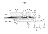
In the following, a third embodiment will be described. The third embodiment is directed to an optical module in which a printed circuit board 340 has a groove 343 as illustrated in FIG. 8 and FIGS. 9A through 9C, rather than an adhesive sheet or a lens sheet having a groove. The optical module according to the present embodiment will be described with reference to FIG. 8 and FIGS. 9A through 9C.
The printed circuit board 340 has a metal layer 342 a formed on one face 340 a thereof for providing conductive tracks and the like, and has a metal layer 342 b on the other face 340 b thereof for providing conductive tracks and the like. FIG. 8 is a cross-sectional view of the optical module of the present embodiment. FIG. 9A is a top view of the printed circuit board 340. FIG. 9B is a bottom view of the printed circuit board 340. FIG. 9C is a cross-sectional view of the printed circuit board 340 taken along a dashed line 9A-9B in FIG. 9B.
In the optical module of the present embodiment, the printed circuit board 340 has a penetrating hole 341 at the position of a light path for light emitted by the light emitting device 50 and for light entering the light receiving device 60. The area of the face 340 b of the printed circuit board 340 where the lens sheet 30 is bonded has the groove 343 that is formed by removing part of the metal layer 342 b. The face 30 a of the lens sheet 30 and the face 340 b of the printed circuit board 340 are bonded to each other via an adhesive sheet 90. The face 340 a of the printed circuit board 340 has the light emitting device 50, the light receiving device 60, the driver 71, and the TIA 72 mounted thereon.
In the optical module of the present embodiment, a space 392 constituted by the penetrating hole 341 of the printed circuit board 340 and the penetrating hole 91 of the adhesive sheet 90 is created between the lens sheet 30 and the light emitting device 50 or the light receiving device 60. The space 92 is not hermetic, and is in communication with the outside through the groove 343 of the printed circuit board 340. The portion of the face 340 b of the printed circuit board 340 where the groove 343 is formed is not in contact with the adhesive sheet 90, so that moisture inside the space 392 may escape to the outside of the space 392 through the groove 233.
Alternatively, as illustrated in FIGS. 10A through 10C, part of the metal layer 342 b may be removed in the area of the face 340 b of the printed circuit board 340 where the lens sheet 30 is bonded, such that the removed area may be situated at the position corresponding to the conductive tracks formed in the metal layer 342 a between the light receiving device 60 and the TIA 72. In this case, the metal layer 342 b of the printed circuit board 340 is coupled to a ground potential, thereby serving as a ground electrode. In the present embodiment, part of the metal layer 342 b serving as a ground electrode is removed at the same horizontal position as the conductive tracks between the light receiving device 60 and the TIA 72 to increase the inductance of the signal tracks, thereby improving frequency characteristic through inductor peaking. Accordingly, the provision of the groove 344 serves both to prevent dew condensation and to improve the frequency characteristics of the optical module. It may be noted that the groove 344 is formed such as to extend beyond the area where the lens sheet is bonded.
Configurations other than those described above are the same as or similar to those of the first embodiment.
Fourth Embodiment
In the following, a fourth embodiment will be described. The fourth embodiment is directed to the configuration in which an adhesive sheet has an uneven surface.
In the optical module of the present embodiment, one face of an adhesive sheet 490 has straight-line ridges and furrows 493 formed therein as illustrated in FIGS. 11A and 11B. FIG. 11A is a top view of the adhesive sheet 490 bonded to the lens sheet 30. FIG. 11B is a cross-sectional view of the adhesive sheet 490 taken along a dashed line 11A-11B in FIG. 11A.
The provision of the straight-line ridges and furrows 493 in the surface of the adhesive sheet 490 creates gaps between the printed circuit board 40 and the face of the adhesive sheet 490 having the ridges and furrows 493. Specifically, mounting the printed circuit board 40 on the adhesive sheet 490 causes the ridge portions of the ridges and furrows 493 to come in contact with the printed circuit board 40, without the furrow portions of the ridges and furrows 493 coming in contact with the printed circuit board 40. This creates gaps between the printed circuit board 40 and the furrow portions of the ridges and furrows 493. The space 192 is thus connected to the outside through these gaps without the provision of a structured groove formed in the adhesive sheet.
As illustrated in FIGS. 12A and 12B, an adhesive sheet 590 may have random bumps 593 formed on the surface thereof. This arrangement brings about the same or similar results and effects as in the case of FIGS. 11A and 11B. FIG. 12A is a top view of the adhesive sheet 590. FIG. 12B is a cross-sectional view of the adhesive sheet 590 taken along a dashed line 12A and 12B in FIG. 12A.
Configurations other than those described above are the same as or similar to those of the first embodiment.
Fifth Embodiment
In the following, a fifth embodiment will be described. The fifth embodiment is directed to the configuration in which the lens sheet has an uneven surface.
In the optical module of the present embodiment, one face of a lens sheet 430 has straight-line ridges and furrows 433 formed therein as illustrated in FIGS. 13A and 13B. FIG. 13A is a top view of the lens sheet 430. FIG. 13B is a cross-sectional view of the lens sheet 430 taken along a dashed line 13A and 13B in FIG. 13A.
The provision of the straight-line ridges and furrows 433 in the surface of the lens sheet 430 creates gaps between the adhesive sheet 90 and the face of the lens sheet 430 having the ridges and furrows 433. Mounting the adhesive sheet 90 on the lens sheet 430 causes the ridge portions of the ridges and furrows 433 to come in contact with the adhesive sheet 90, without the furrow portions of the ridges and furrows 433 coming in contact with the adhesive sheet 90. This creates gaps between the adhesive sheet 90 and the furrow portions of the ridges and furrows 433. Accordingly, the space 292 is connected to the outside through the gaps between the furrow portions and the adhesive sheet 90, without the provision of a structured groove formed in the lens sheet.
As illustrated in FIGS. 14A and 14B, a lens sheet 530 may have random bumps 533 formed on the surface thereof. This arrangement brings about the same or similar results and effects as in the case of FIGS. 13A and 13B. FIG. 14A is a top view of the lens sheet 530. FIG. 14B is a cross-sectional view of the lens sheet 530 taken along a dashed line 14A and 14B in FIG. 14A.
Configurations other than those described above are the same as or similar to those of the second embodiment.
Sixth Embodiment
In the following, a sixth embodiment will be described. The sixth embodiment is directed to the configuration in which the printed circuit board has an uneven surface.
In the optical module of the present embodiment, one face of a printed circuit board 440 has straight-line ridges and furrows 443 formed therein as illustrated in FIGS. 15A and 15B. FIG. 15A is a bottom view of the printed circuit board 440. FIG. 15B is a cross-sectional view of the printed circuit board 440 taken along a dashed line 15A and 15B in FIG. 15A.
The provision of the straight-line ridges and furrows 433 in the surface of the printed circuit board 440 creates gaps between the adhesive sheet 90 and the face of the printed circuit board 440 having the ridges and furrows 443. Mounting the printed circuit board 440 on the adhesive sheet 90 causes the ridge portions of the ridges and furrows 443 to come in contact with the adhesive sheet 90, without the furrow portions coming in contact with the adhesive sheet 90. This creates gaps between the adhesive sheet 90 and the furrow portions of the ridges and furrows 433. Accordingly, the space 392 is connected to the outside through the gaps between the furrow portions and the adhesive sheet 90, without the provision of a structured groove formed in the printed circuit board.
As illustrated in FIGS. 16A and 16B, a printed circuit board 540 may have random bumps 543 formed on the surface thereof. This arrangement also brings about the same or similar results and effects as in the case of FIGS. 15A and 15B. FIG. 16A is a bottom view of the printed circuit board 540. FIG. 16B is a cross-sectional view of the printed circuit board 540 taken along a dashed line 16A and 16B in FIG. 16A.
Configurations other than those described above are the same as or similar to those of the third embodiment.
Further, although a description has been given with respect to one or more embodiments of the present invention, the contents of such a description do not limit the scope of the invention.
The present application is based on and claims the benefit of priority of Japanese priority application No. 2016-136641 filed on Jul. 11, 2016, with the Japanese Patent Office, the entire contents of which are hereby incorporated by reference.

Claims (5)

What is claimed is:
1. An optical module, comprising:
a lens sheet having one or more lenses formed thereon;
a substrate having a photoelectric conversion device mounted on a first face thereof and having a first penetrating hole formed therethrough between the photoelectric conversion device and the one or more lenses; and
an adhesive layer configured to bond a face of the lens sheet to a second face of the substrate,
wherein the adhesive layer has a second penetrating hole formed therethrough between the one or more lenses and the photoelectric conversion device, and a pathway is provided to connect a space constituted by the first penetrating hole and the second penetrating hole to an outside of the space,
wherein an outer perimeter, below the one or more lenses, of the lens sheet encompasses an entirety of the second penetrating hole in a plan view as viewed in a thickness direction of the lens sheet, and
wherein an outer perimeter of the adhesive layer encompasses an entirety of the second penetrating hole in the plan view, and the pathway extends along or in the adhesive layer to connect the second penetrating hole to an outside of the outer perimeter of the adhesive layer in the plan view.
2. The optical module as claimed in claim 1, wherein the pathway is formed in the adhesive layer.
3. The optical module as claimed in claim 1, wherein the pathway is formed in the lens sheet.
4. The optical module as claimed in claim 1, wherein the pathway is formed in the substrate.
5. The optical module as claimed in claim 1, further comprising:
an optical waveguide having a mirror formed thereon; and
a second adhesive layer configured to bond a face of the optical waveguide to another face of the lens sheet.
US15/635,610 2016-07-11 2017-06-28 Optical module Expired - Fee Related US10078189B2 (en)

Applications Claiming Priority (2)

Application Number Priority Date Filing Date Title
JP2016136641A JP2018010030A (en) 2016-07-11 2016-07-11 Optical module
JP2016-136641 2016-07-11

Publications (2)

Publication Number Publication Date
US20180011264A1 US20180011264A1 (en) 2018-01-11
US10078189B2 true US10078189B2 (en) 2018-09-18

Family

ID=60892918

Family Applications (1)

Application Number Title Priority Date Filing Date
US15/635,610 Expired - Fee Related US10078189B2 (en) 2016-07-11 2017-06-28 Optical module

Country Status (2)

Country Link
US (1) US10078189B2 (en)
JP (1) JP2018010030A (en)

Cited By (1)

* Cited by examiner, † Cited by third party
Publication number Priority date Publication date Assignee Title
US10659169B2 (en) * 2018-08-10 2020-05-19 Fujitsu Limited Optical transmitter

Families Citing this family (1)

* Cited by examiner, † Cited by third party
Publication number Priority date Publication date Assignee Title
JP2018017861A (en) * 2016-07-27 2018-02-01 富士通コンポーネント株式会社 Optical module

Citations (15)

* Cited by examiner, † Cited by third party
Publication number Priority date Publication date Assignee Title
US20050041906A1 (en) * 2001-02-28 2005-02-24 Akio Sugama Optical wiring substrate, method of manufacturing optical wiring substrate and multilayer optical wiring
JP2005322809A (en) 2004-05-10 2005-11-17 Sharp Corp Semiconductor device, method for manufacturing the same, and module for optical device
US20110317958A1 (en) * 2010-06-29 2011-12-29 Lightwire, Inc. Vent Structures For Encapsulated Components On An SOI-Based Photonics Platform
JP2012068539A (en) 2010-09-24 2012-04-05 Fujitsu Ltd Optical module and manufacturing method thereof
WO2013105470A1 (en) 2012-01-10 2013-07-18 日立化成株式会社 Optical waveguide with mirror, optical fiber connector, and manufacturing method thereof
US20130315543A1 (en) * 2012-05-23 2013-11-28 Kuo-Fong Tseng Optical-electrical conversion module and optical transmission connecting assembly using the same
US20140140657A1 (en) * 2012-11-20 2014-05-22 Fujitsu Limited Optical module and fabrication method
JP2014164198A (en) * 2013-02-26 2014-09-08 Fujitsu Component Ltd Optical communication device
US8827572B2 (en) * 2009-03-26 2014-09-09 Wuhan Telecommunication Devices Co., Ltd. Side coupling optical fiber assembly and fabrication method thereof
US20140290850A1 (en) * 2013-03-28 2014-10-02 Fujitsu Limited Bonding apparatus and bonding method
US20150212285A1 (en) * 2014-01-28 2015-07-30 Fujitsu Limited Optical module, method for manufacturing optical module, and optical transceiver
US20160341903A1 (en) * 2015-02-12 2016-11-24 Source Photonics (Chengdu) Co., Ltd. Integrated Lens With Multiple Optical Structures and/or Surfaces, Optical Module and Transceiver Including the Same, and Methods of Making and Using the Same
US20160349469A1 (en) * 2015-06-01 2016-12-01 Fujitsu Limited Manufacturing method of printed circuit board, printed circuit board, and optical device
US20170068057A1 (en) * 2015-09-04 2017-03-09 Ccs Technology, Inc. Fiber coupling device for coupling of at least one optical fiber
US20170068056A1 (en) * 2015-09-03 2017-03-09 Fujitsu Component Limited Device mounting apparatus and device mounting method

Patent Citations (19)

* Cited by examiner, † Cited by third party
Publication number Priority date Publication date Assignee Title
US20050041906A1 (en) * 2001-02-28 2005-02-24 Akio Sugama Optical wiring substrate, method of manufacturing optical wiring substrate and multilayer optical wiring
JP2005322809A (en) 2004-05-10 2005-11-17 Sharp Corp Semiconductor device, method for manufacturing the same, and module for optical device
US7456483B2 (en) 2004-05-10 2008-11-25 Sharp Kabushiki Kaisha Semiconductor device, manufacturing method of semiconductor device and module for optical device
US8827572B2 (en) * 2009-03-26 2014-09-09 Wuhan Telecommunication Devices Co., Ltd. Side coupling optical fiber assembly and fabrication method thereof
US20110317958A1 (en) * 2010-06-29 2011-12-29 Lightwire, Inc. Vent Structures For Encapsulated Components On An SOI-Based Photonics Platform
US8774576B2 (en) 2010-09-24 2014-07-08 Fujitsu Limited Optical module and method for manufacturing the same
JP2012068539A (en) 2010-09-24 2012-04-05 Fujitsu Ltd Optical module and manufacturing method thereof
US9442251B2 (en) 2012-01-10 2016-09-13 Hitachi Chemical Company, Ltd. Optical waveguide with mirror, optical fiber connector, and manufacturing method thereof
WO2013105470A1 (en) 2012-01-10 2013-07-18 日立化成株式会社 Optical waveguide with mirror, optical fiber connector, and manufacturing method thereof
US20130315543A1 (en) * 2012-05-23 2013-11-28 Kuo-Fong Tseng Optical-electrical conversion module and optical transmission connecting assembly using the same
US20140140657A1 (en) * 2012-11-20 2014-05-22 Fujitsu Limited Optical module and fabrication method
JP2014164198A (en) * 2013-02-26 2014-09-08 Fujitsu Component Ltd Optical communication device
US20140290850A1 (en) * 2013-03-28 2014-10-02 Fujitsu Limited Bonding apparatus and bonding method
US20150212285A1 (en) * 2014-01-28 2015-07-30 Fujitsu Limited Optical module, method for manufacturing optical module, and optical transceiver
JP2015141300A (en) * 2014-01-28 2015-08-03 富士通株式会社 Optical module, manufacturing method of optical module, and optical signal transceiver
US20160341903A1 (en) * 2015-02-12 2016-11-24 Source Photonics (Chengdu) Co., Ltd. Integrated Lens With Multiple Optical Structures and/or Surfaces, Optical Module and Transceiver Including the Same, and Methods of Making and Using the Same
US20160349469A1 (en) * 2015-06-01 2016-12-01 Fujitsu Limited Manufacturing method of printed circuit board, printed circuit board, and optical device
US20170068056A1 (en) * 2015-09-03 2017-03-09 Fujitsu Component Limited Device mounting apparatus and device mounting method
US20170068057A1 (en) * 2015-09-04 2017-03-09 Ccs Technology, Inc. Fiber coupling device for coupling of at least one optical fiber

Cited By (1)

* Cited by examiner, † Cited by third party
Publication number Priority date Publication date Assignee Title
US10659169B2 (en) * 2018-08-10 2020-05-19 Fujitsu Limited Optical transmitter

Also Published As

Publication number Publication date
US20180011264A1 (en) 2018-01-11
JP2018010030A (en) 2018-01-18

Similar Documents

Publication Publication Date Title
US7679095B2 (en) Optoelectric composite substrate and electronic apparatus
US20070051877A1 (en) Optical transmitter-receiver, optical transmitter-receiver module, and optical communication device
US20140099123A1 (en) Flexible printed circuit board and optical communication module including the same
JP7263697B2 (en) Photodetector
JP2012058731A (en) Electro-optical coupler module having optical waveguide structure
KR20070080987A (en) Optical module
US20120207437A1 (en) Optical module
JP2011248361A (en) Signal transmission module having optical waveguide structure
JP2005203553A (en) Optical transmission/reception module and optical transmitter-receiver
US20090074352A1 (en) Bidirectional optical transmission device
US8851733B2 (en) Light signal transmitter and light receiver for an optical sensor
JP5692581B2 (en) Photoelectric conversion module and method for manufacturing photoelectric conversion module
US10078189B2 (en) Optical module
JP5223879B2 (en) Transceiver module
JP2007123739A (en) Optical transmission module, optical transmission/reception module and optical communication apparatus
US20170219787A1 (en) Communication Module
US20070147747A1 (en) Optical module and optical transmission system using the same
JP2004235418A (en) Optical module, optical communication apparatus, photoelectricity mixed loading integrated circuit, circuit board, and electronic apparatus
JP2019179816A (en) Optical reception module, optical module and optical transmission device
US11539446B2 (en) Optical receiver
JP2008145931A (en) Photoelectric composite wiring
JP5117419B2 (en) Parallel transmission module
JP6589345B2 (en) Optical wiring board, optical module, and optical active cable
JP4553026B2 (en) Optical transmission equipment
KR100440431B1 (en) opto-electronic submount for photo electric modules

Legal Events

Date Code Title Description
AS Assignment

Owner name: FUJITSU LIMITED, JAPAN

Free format text: ASSIGNMENT OF ASSIGNORS INTEREST;ASSIGNORS:UCHIYAMA, TAKUYA;AKIEDA, SHINICHIRO;KASE, MARIKO;SIGNING DATES FROM 20170612 TO 20170621;REEL/FRAME:042845/0759

Owner name: FUJITSU COMPONENT LIMITED, JAPAN

Free format text: ASSIGNMENT OF ASSIGNORS INTEREST;ASSIGNORS:UCHIYAMA, TAKUYA;AKIEDA, SHINICHIRO;KASE, MARIKO;SIGNING DATES FROM 20170612 TO 20170621;REEL/FRAME:042845/0759

STCF Information on status: patent grant

Free format text: PATENTED CASE

FEPP Fee payment procedure

Free format text: MAINTENANCE FEE REMINDER MAILED (ORIGINAL EVENT CODE: REM.); ENTITY STATUS OF PATENT OWNER: LARGE ENTITY

LAPS Lapse for failure to pay maintenance fees

Free format text: PATENT EXPIRED FOR FAILURE TO PAY MAINTENANCE FEES (ORIGINAL EVENT CODE: EXP.); ENTITY STATUS OF PATENT OWNER: LARGE ENTITY

STCH Information on status: patent discontinuation

Free format text: PATENT EXPIRED DUE TO NONPAYMENT OF MAINTENANCE FEES UNDER 37 CFR 1.362

FP Lapsed due to failure to pay maintenance fee

Effective date: 20220918