WO2021240962A1 - 光透過性導電性シートの製造方法 - Google Patents
光透過性導電性シートの製造方法 Download PDFInfo
- Publication number
- WO2021240962A1 WO2021240962A1 PCT/JP2021/011147 JP2021011147W WO2021240962A1 WO 2021240962 A1 WO2021240962 A1 WO 2021240962A1 JP 2021011147 W JP2021011147 W JP 2021011147W WO 2021240962 A1 WO2021240962 A1 WO 2021240962A1
- Authority
- WO
- WIPO (PCT)
- Prior art keywords
- target
- light
- transmitting conductive
- layer
- film forming
- Prior art date
- Legal status (The legal status is an assumption and is not a legal conclusion. Google has not performed a legal analysis and makes no representation as to the accuracy of the status listed.)
- Ceased
Links
Images


Classifications
-
- C—CHEMISTRY; METALLURGY
- C23—COATING METALLIC MATERIAL; COATING MATERIAL WITH METALLIC MATERIAL; CHEMICAL SURFACE TREATMENT; DIFFUSION TREATMENT OF METALLIC MATERIAL; COATING BY VACUUM EVAPORATION, BY SPUTTERING, BY ION IMPLANTATION OR BY CHEMICAL VAPOUR DEPOSITION, IN GENERAL; INHIBITING CORROSION OF METALLIC MATERIAL OR INCRUSTATION IN GENERAL
- C23C—COATING METALLIC MATERIAL; COATING MATERIAL WITH METALLIC MATERIAL; SURFACE TREATMENT OF METALLIC MATERIAL BY DIFFUSION INTO THE SURFACE, BY CHEMICAL CONVERSION OR SUBSTITUTION; COATING BY VACUUM EVAPORATION, BY SPUTTERING, BY ION IMPLANTATION OR BY CHEMICAL VAPOUR DEPOSITION, IN GENERAL
- C23C14/00—Coating by vacuum evaporation, by sputtering or by ion implantation of the coating forming material
- C23C14/22—Coating by vacuum evaporation, by sputtering or by ion implantation of the coating forming material characterised by the process of coating
- C23C14/34—Sputtering
- C23C14/3464—Sputtering using more than one target
-
- B—PERFORMING OPERATIONS; TRANSPORTING
- B32—LAYERED PRODUCTS
- B32B—LAYERED PRODUCTS, i.e. PRODUCTS BUILT-UP OF STRATA OF FLAT OR NON-FLAT, e.g. CELLULAR OR HONEYCOMB, FORM
- B32B37/00—Methods or apparatus for laminating, e.g. by curing or by ultrasonic bonding
- B32B37/14—Methods or apparatus for laminating, e.g. by curing or by ultrasonic bonding characterised by the properties of the layers
-
- B—PERFORMING OPERATIONS; TRANSPORTING
- B32—LAYERED PRODUCTS
- B32B—LAYERED PRODUCTS, i.e. PRODUCTS BUILT-UP OF STRATA OF FLAT OR NON-FLAT, e.g. CELLULAR OR HONEYCOMB, FORM
- B32B7/00—Layered products characterised by the relation between layers; Layered products characterised by the relative orientation of features between layers, or by the relative values of a measurable parameter between layers, i.e. products comprising layers having different physical, chemical or physicochemical properties; Layered products characterised by the interconnection of layers
- B32B7/02—Physical, chemical or physicochemical properties
- B32B7/023—Optical properties
-
- B—PERFORMING OPERATIONS; TRANSPORTING
- B32—LAYERED PRODUCTS
- B32B—LAYERED PRODUCTS, i.e. PRODUCTS BUILT-UP OF STRATA OF FLAT OR NON-FLAT, e.g. CELLULAR OR HONEYCOMB, FORM
- B32B9/00—Layered products comprising a layer of a particular substance not covered by groups B32B11/00 - B32B29/00
-
- C—CHEMISTRY; METALLURGY
- C23—COATING METALLIC MATERIAL; COATING MATERIAL WITH METALLIC MATERIAL; CHEMICAL SURFACE TREATMENT; DIFFUSION TREATMENT OF METALLIC MATERIAL; COATING BY VACUUM EVAPORATION, BY SPUTTERING, BY ION IMPLANTATION OR BY CHEMICAL VAPOUR DEPOSITION, IN GENERAL; INHIBITING CORROSION OF METALLIC MATERIAL OR INCRUSTATION IN GENERAL
- C23C—COATING METALLIC MATERIAL; COATING MATERIAL WITH METALLIC MATERIAL; SURFACE TREATMENT OF METALLIC MATERIAL BY DIFFUSION INTO THE SURFACE, BY CHEMICAL CONVERSION OR SUBSTITUTION; COATING BY VACUUM EVAPORATION, BY SPUTTERING, BY ION IMPLANTATION OR BY CHEMICAL VAPOUR DEPOSITION, IN GENERAL
- C23C14/00—Coating by vacuum evaporation, by sputtering or by ion implantation of the coating forming material
- C23C14/0021—Reactive sputtering or evaporation
- C23C14/0036—Reactive sputtering
-
- C—CHEMISTRY; METALLURGY
- C23—COATING METALLIC MATERIAL; COATING MATERIAL WITH METALLIC MATERIAL; CHEMICAL SURFACE TREATMENT; DIFFUSION TREATMENT OF METALLIC MATERIAL; COATING BY VACUUM EVAPORATION, BY SPUTTERING, BY ION IMPLANTATION OR BY CHEMICAL VAPOUR DEPOSITION, IN GENERAL; INHIBITING CORROSION OF METALLIC MATERIAL OR INCRUSTATION IN GENERAL
- C23C—COATING METALLIC MATERIAL; COATING MATERIAL WITH METALLIC MATERIAL; SURFACE TREATMENT OF METALLIC MATERIAL BY DIFFUSION INTO THE SURFACE, BY CHEMICAL CONVERSION OR SUBSTITUTION; COATING BY VACUUM EVAPORATION, BY SPUTTERING, BY ION IMPLANTATION OR BY CHEMICAL VAPOUR DEPOSITION, IN GENERAL
- C23C14/00—Coating by vacuum evaporation, by sputtering or by ion implantation of the coating forming material
- C23C14/06—Coating by vacuum evaporation, by sputtering or by ion implantation of the coating forming material characterised by the coating material
- C23C14/08—Oxides
-
- C—CHEMISTRY; METALLURGY
- C23—COATING METALLIC MATERIAL; COATING MATERIAL WITH METALLIC MATERIAL; CHEMICAL SURFACE TREATMENT; DIFFUSION TREATMENT OF METALLIC MATERIAL; COATING BY VACUUM EVAPORATION, BY SPUTTERING, BY ION IMPLANTATION OR BY CHEMICAL VAPOUR DEPOSITION, IN GENERAL; INHIBITING CORROSION OF METALLIC MATERIAL OR INCRUSTATION IN GENERAL
- C23C—COATING METALLIC MATERIAL; COATING MATERIAL WITH METALLIC MATERIAL; SURFACE TREATMENT OF METALLIC MATERIAL BY DIFFUSION INTO THE SURFACE, BY CHEMICAL CONVERSION OR SUBSTITUTION; COATING BY VACUUM EVAPORATION, BY SPUTTERING, BY ION IMPLANTATION OR BY CHEMICAL VAPOUR DEPOSITION, IN GENERAL
- C23C14/00—Coating by vacuum evaporation, by sputtering or by ion implantation of the coating forming material
- C23C14/06—Coating by vacuum evaporation, by sputtering or by ion implantation of the coating forming material characterised by the coating material
- C23C14/08—Oxides
- C23C14/086—Oxides of zinc, germanium, cadmium, indium, tin, thallium or bismuth
-
- C—CHEMISTRY; METALLURGY
- C23—COATING METALLIC MATERIAL; COATING MATERIAL WITH METALLIC MATERIAL; CHEMICAL SURFACE TREATMENT; DIFFUSION TREATMENT OF METALLIC MATERIAL; COATING BY VACUUM EVAPORATION, BY SPUTTERING, BY ION IMPLANTATION OR BY CHEMICAL VAPOUR DEPOSITION, IN GENERAL; INHIBITING CORROSION OF METALLIC MATERIAL OR INCRUSTATION IN GENERAL
- C23C—COATING METALLIC MATERIAL; COATING MATERIAL WITH METALLIC MATERIAL; SURFACE TREATMENT OF METALLIC MATERIAL BY DIFFUSION INTO THE SURFACE, BY CHEMICAL CONVERSION OR SUBSTITUTION; COATING BY VACUUM EVAPORATION, BY SPUTTERING, BY ION IMPLANTATION OR BY CHEMICAL VAPOUR DEPOSITION, IN GENERAL
- C23C14/00—Coating by vacuum evaporation, by sputtering or by ion implantation of the coating forming material
- C23C14/22—Coating by vacuum evaporation, by sputtering or by ion implantation of the coating forming material characterised by the process of coating
- C23C14/56—Apparatus specially adapted for continuous coating; Arrangements for maintaining the vacuum, e.g. vacuum locks
- C23C14/562—Apparatus specially adapted for continuous coating; Arrangements for maintaining the vacuum, e.g. vacuum locks for coating elongated substrates
-
- C—CHEMISTRY; METALLURGY
- C23—COATING METALLIC MATERIAL; COATING MATERIAL WITH METALLIC MATERIAL; CHEMICAL SURFACE TREATMENT; DIFFUSION TREATMENT OF METALLIC MATERIAL; COATING BY VACUUM EVAPORATION, BY SPUTTERING, BY ION IMPLANTATION OR BY CHEMICAL VAPOUR DEPOSITION, IN GENERAL; INHIBITING CORROSION OF METALLIC MATERIAL OR INCRUSTATION IN GENERAL
- C23C—COATING METALLIC MATERIAL; COATING MATERIAL WITH METALLIC MATERIAL; SURFACE TREATMENT OF METALLIC MATERIAL BY DIFFUSION INTO THE SURFACE, BY CHEMICAL CONVERSION OR SUBSTITUTION; COATING BY VACUUM EVAPORATION, BY SPUTTERING, BY ION IMPLANTATION OR BY CHEMICAL VAPOUR DEPOSITION, IN GENERAL
- C23C14/00—Coating by vacuum evaporation, by sputtering or by ion implantation of the coating forming material
- C23C14/58—After-treatment
- C23C14/5806—Thermal treatment
-
- H—ELECTRICITY
- H01—ELECTRIC ELEMENTS
- H01B—CABLES; CONDUCTORS; INSULATORS; SELECTION OF MATERIALS FOR THEIR CONDUCTIVE, INSULATING OR DIELECTRIC PROPERTIES
- H01B5/00—Non-insulated conductors or conductive bodies characterised by their form
- H01B5/14—Non-insulated conductors or conductive bodies characterised by their form comprising conductive layers or films on insulating-supports
Definitions
- the present invention relates to a method for manufacturing a light transmissive conductive sheet.
- a transparent conductive film having a transparent conductive film made of ITO on the surface of a base film is known.
- the transparent conductive film is required to have a low resistivity.
- the transparent conductive film described in Patent Document 1 has a problem that the above-mentioned requirements cannot be satisfied.
- the present invention provides a method for manufacturing a light-transmitting conductive sheet provided with a light-transmitting conductive layer having a low resistivity.
- the present invention (1) comprises a step of forming a light-transmitting conductive layer on one surface in the thickness direction of a base sheet by a plurality of times of sputtering in which electric power is applied to each of a plurality of targets, and the light-transmitting property is described.
- the step of forming the conductive layer is a first target contained in the plurality of targets, and is an indium-tin composite oxide containing indium oxide and tin oxide, and the content of the tin oxide exceeds 8% by mass.
- the ratio (P1 / P) of the power density P1 in the first target to the total power density P in the plurality of targets is 0.
- a method for producing a light-transmitting conductive sheet having a value of 20 or less is included.
- the ratio (P1 / P) of the power density P1 in the first target to the total power density P in the plurality of targets is 0.20 or less, so that the inner layer is used.
- a dense outer layer can be formed, thereby reducing the specific resistance of the light-transmitting conductive layer.
- this method for producing a light-transmitting conductive sheet electric power is applied to a first target made of an indium-tin composite oxide having a tin oxide content of more than 8% by mass to form an inner layer.
- the specific resistance of the light-transmitting conductive layer can be sufficiently reduced.
- the first step sputtering is performed in an atmosphere of a sputtering gas containing a reactive gas
- sputtering is performed in an atmosphere of a sputtering gas containing a reactive gas
- the second step sputtering is performed in an atmosphere of a sputtering gas containing a reactive gas.
- the light according to (1), wherein the ratio (R1 / R2) of the ratio R1 of the reactive gas in the sputtering gas in the first step to the ratio R2 of the reactive gas in the sputtering gas in the step is 1 or less.
- the manufacturing method of the present invention it is possible to manufacture a light-transmitting conductive sheet provided with a light-transmitting conductive layer having a low resistivity.
- FIG. 1 is a schematic view of a sputtering apparatus used in one embodiment of the method for manufacturing a light-transmitting conductive sheet of the present invention.
- FIG. 2 is a cross-sectional view of a light-transmitting conductive sheet manufactured by the sputtering apparatus of FIG.
- FIG. 3 is a schematic view of a modified example of the sputtering apparatus shown in FIG.
- FIG. 4 is a cross-sectional view of a light transmissive conductive sheet manufactured by the sputtering apparatus of FIG.
- FIG. 5 is an image processing diagram of the TEM photograph of Example 1.
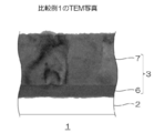
- FIG. 6 is an image processing diagram of the TEM photograph of Comparative Example 1.
- the light-transmitting conductive layer 3 is formed on one surface of the base sheet 2 in the thickness direction by sputtering in which electric power is applied to each of a plurality of targets 51, 52, 53, 54.
- the plurality of targets 51, 52, 53, 54 include the first target 51, the second target 52, the third target 53, and the fourth target 54.
- the sputtering apparatus 30 used for sputtering will be described. As shown in FIG. 1, the sputtering apparatus 30 includes a feeding section 35, a sputtering section 36, and a winding section 37 in this order.
- the feeding unit 35 includes a feeding roll 38.
- the sputter portion 36 includes a film forming roll 40, a first film forming chamber 41, and a plurality of film forming chambers 42, 43, 44.
- the plurality of film forming chambers 42, 43, 44 are a second film forming chamber 42, a third film forming chamber 43, and a fourth film forming chamber 44.
- the film forming roll 40 includes a cooling device (not shown) configured to cool the film forming roll 40.
- the first film forming chamber 41 accommodates the first target 51, the first gas supply machine 61, and the discharge port of the first pump 91.
- the first target 51, the first gas supply machine 61, and the discharge port of the first pump 91 are arranged at intervals with respect to the film forming roll 40.
- a magnet (not shown) is arranged on the opposite side of the film forming roll 40 with respect to the first target 51.
- the magnetic field strength of the magnet is adjusted so that the horizontal magnetic field strength on the first target 51 is, for example, 10 mT or more and 200 mT or less.
- the material of the first target 51 is ITO (indium-tin composite oxide).
- ITO contains indium oxide and tin oxide.
- the tin oxide content in ITO exceeds 8% by mass. On the other hand, if the tin oxide content is 8% by mass or less, the specific resistance of the light-transmitting conductive layer 3 cannot be sufficiently reduced.
- the content of tin oxide in ITO is preferably 8.5% by mass or more, more preferably 9% by mass or more, still more preferably 9.5% by mass or more, and for example, 30% by mass or less. It is preferably 25% by mass or less, more preferably 20% by mass or less, still more preferably 15% by mass or less. If the tin oxide content is not more than the above upper limit, the resistivity can be stably reduced.
- the content of indium oxide in ITO is the balance of the content of tin oxide.
- the ITO is, if necessary, at least one selected from the group consisting of Zn, Ga, Sb, Ti, Si, Zr, Mg, Al, Au, Ag, Cu, Pd and W in a trace amount (for example, for example). 5% by mass or less) may be doped.
- the material of the first target 51 contains a sintered body of a conductive oxide.
- the first gas supply machine 61 is configured to supply the sputtering gas to the first film forming chamber 41.
- the sputtering gas include an inert gas such as nitrogen, argon, krypton, and xenone, for example, a mixed gas containing an inert gas and a reactive gas such as oxygen, and a mixed gas is preferable. Be done. If the sputtering gas is a mixed gas, the first gas supply machine 61 includes the first inert gas supply machine 71 and the first reactive gas supply machine 72, from which the inert gas and the reaction are carried out. The inert gas is supplied to the first film forming chamber 41.
- the second film forming chamber 42 is arranged adjacent to the first film forming chamber 41 in the circumferential direction of the film forming roll 40.
- the second film forming chamber 42 accommodates the second target 52 as an example of the target, the second gas supply machine 62, and the discharge port of the second pump 92.
- the second target 52, the second gas supply machine 62, and the discharge port of the second pump 92 are arranged at intervals with respect to the film forming roll 40.
- a magnet (not shown) is arranged on the opposite side of the film forming roll 40 with respect to the second target 52.
- the magnetic field strength of the magnet is adjusted so that the horizontal magnetic field strength on the second target 52 is, for example, 10 mT or more and 200 mT or less.
- the material of the second target 52 is ITO.
- the content of tin oxide in ITO is not particularly limited.
- the content of tin oxide in ITO is, for example, 1% by mass or more, preferably 5% by mass or more, more preferably 8% by mass or more, and for example, 30% by mass or less, preferably 25% by mass. Hereinafter, it is more preferably 20% by mass or less, still more preferably 15% by mass or less.
- the tin oxide content in the material of the second target 52 is the same as the tin oxide content in the material of the first target 51.
- the material of the second target 52 includes a sintered body of a conductive oxide.
- the second gas supply machine 62 is configured to supply the sputtering gas to the second film forming chamber 42.
- the sputtering gas include the above-mentioned inert gas and the above-mentioned mixed gas, and preferably the above-mentioned mixed gas. If the sputtering gas is a mixed gas, the second gas supply machine 62 includes the second inert gas supply machine 73 and the second reactive gas supply machine 74, and reacts with the inert gas from each of them. The inert gas is supplied to the second film forming chamber 42.
- the third film forming chamber 43 is adjacent to the third film forming chamber 43 in the circumferential direction of the film forming roll 40, and is arranged on the opposite side of the first film forming chamber 41 with respect to the second film forming chamber 42. ..
- the third film forming chamber 43 accommodates the third target 53 as an example of the target, the third gas supply machine 63, and the discharge port of the third pump 93.
- the third target 53, the third gas supply machine 63, and the discharge port of the third pump 93 are arranged at intervals with respect to the film forming roll 40.
- a magnet (not shown) is arranged on the opposite side of the film forming roll 40 with respect to the third target 53.
- the magnetic field strength of the magnet is adjusted so that the horizontal magnetic field strength is, for example, 10 mT or more and 200 mT or less.
- the material of the third target 53 is ITO.
- the content of tin oxide in ITO is not particularly limited.
- the content of tin oxide in ITO is, for example, 1% by mass or more, preferably 5% by mass or more, more preferably 8% by mass or more, and for example, 30% by mass or less, preferably 25% by mass. Hereinafter, it is more preferably 20% by mass or less, still more preferably 15% by mass or less.
- the tin oxide content in the material of the third target 53 is the same as the tin oxide content in the material of the first target 51.
- the material of the third target 53 includes a sintered body of a conductive oxide.
- the third gas supply machine 63 is configured to supply the sputtering gas to the third film forming chamber 43.
- the sputtering gas include the above-mentioned inert gas and the above-mentioned mixed gas, and preferably the above-mentioned mixed gas. If the sputtering gas is a mixed gas, the third gas supply machine 63 includes the third inert gas supply machine 75 and the third reactive gas supply machine 76, from which the inert gas and the reaction occur. The inert gas is supplied to the third film forming chamber 43.
- the fourth film forming chamber 44 is adjacent to the third film forming chamber 43 in the circumferential direction of the film forming roll 40, and is arranged on the opposite side of the second film forming chamber 42 with respect to the third film forming chamber 43.
- the fourth film forming chamber 44 accommodates the fourth target 54 as an example of the target, the fourth gas supply machine 64, and the discharge port of the fourth pump 94.
- the fourth target 54, the fourth gas supply device 64, and the discharge port of the fourth pump 94 are arranged at intervals with respect to the film forming roll 40.
- a magnet (not shown) is arranged on the opposite side of the film forming roll 40 with respect to the fourth target 54.
- the magnetic field strength of the magnet is adjusted so that the horizontal magnetic field strength is, for example, 10 mT or more and 200 mT or less.
- the material of the 4th target 54 is ITO.
- the content of tin oxide in ITO is not particularly limited.
- the content of tin oxide in ITO is, for example, 1% by mass or more, preferably 5% by mass or more, more preferably 8% by mass or more, and for example, 30% by mass or less, preferably 25% by mass. Hereinafter, it is more preferably 20% by mass or less, still more preferably 15% by mass or less.
- the tin oxide content in the material of the fourth target 54 is the same as the tin oxide content in the material of the first target 51.
- the material of the fourth target 54 contains a sintered body of a conductive oxide.
- the fourth gas supply machine 64 is configured to supply the sputtering gas to the fourth film forming chamber 44.
- the sputtering gas include the above-mentioned inert gas and the above-mentioned mixed gas, and preferably the above-mentioned mixed gas. If the sputtering gas is a mixed gas, the fourth gas supply machine 64 includes the fourth inert gas supply machine 77 and the fourth reactive gas supply machine 78, from which the inert gas and the reaction occur. The inert gas is supplied to the fourth film forming chamber 44.
- the take-up unit 37 includes a take-up roll 39.
- Step of forming a light-transmitting conductive layer on a base sheet Next, the step of forming the light-transmitting conductive layer 3 on the base sheet 2 by the sputtering apparatus 30 will be specifically described.
- the base sheet 2 is prepared.
- the base material sheet 2 has a thickness and extends in a plane direction orthogonal to the thickness direction. Specifically, the base sheet 2 has a film shape extending in the plane direction. The base sheet 2 has flexibility.
- the base material sheet 2 includes at least the base material layer 4. Specifically, the base material sheet 2 includes the base material layer 4 and the hard coat layer 5 in order toward one side in the thickness direction. In this embodiment, the number of base sheet 2 provided in the light transmissive conductive sheet 1 is 1.
- the base material layer 4 has a film shape extending in the plane direction.
- the base material layer 4 forms the other surface of the base material sheet 2 in the thickness direction.
- the material of the base material layer 4 is not particularly limited, and examples thereof include polymers and glass. Preferred are polymers. Examples of the polymer include olefin resins such as polyethylene, polypropylene and cycloolefin polymer (COP), and polyester resins such as polyethylene terephthalate (PET), polybutylene terephthalate and polyethylene naphthalate, for example, polyacrylate and / or polymethacrylate.
- COP polypropylene and cycloolefin polymer
- PET polyethylene terephthalate
- PET polybutylene terephthalate
- polyethylene naphthalate for example, polyacrylate and / or polymethacrylate.
- (Meta) acrylic resins (acrylic resins and / or methacrylic resins) such as, for example, polycarbonate resins, polyether sulfone resins, polyarylate resins, melamine resins, polyamide resins, polyimide resins, cellulose resins, polystyrene resins and the like.
- a polyester resin is preferable, and PET is more preferable.
- the thickness of the base material layer 4 is, for example, 1 ⁇ m or more, preferably 10 ⁇ m or more, more preferably 30 ⁇ m or more, and for example, 300 ⁇ m or less, preferably 100 ⁇ m or less, more preferably 75 ⁇ m or less.
- the hard coat layer 5 is a scratch protection layer for making it difficult for the light-transmitting conductive layer 3 to be scratched.
- the hard coat layer 5 forms one side of the base sheet 2 in the thickness direction.
- the hard coat layer 5 is in contact with all of one surface of the base material layer 4 in the thickness direction.
- Examples of the material of the hard coat layer 5 include a cured product of the hard coat composition (acrylic resin, urethane resin, etc.) described in JP-A-2016-179686.
- the thickness of the hard coat layer 5 is, for example, 0.1 ⁇ m or more, preferably 0.5 ⁇ m or more, and for example, 10 ⁇ m or less, preferably 5 ⁇ m or less.
- the thickness of the base sheet 2 is, for example, 1 ⁇ m or more, preferably 10 ⁇ m or more, more preferably 15 ⁇ m or more, still more preferably 30 ⁇ m or more, and for example, 310 ⁇ m or less, preferably 210 or less, more preferably. Is 110 ⁇ m or less, more preferably 80 ⁇ m or less.
- the total light transmittance (JIS K 7375-2008) of the base sheet 2 is, for example, 60% or more, preferably 80% or more, more preferably 85% or more, and for example, 100% or less. ..
- the base sheet 2 is set in the sputtering apparatus 30. Specifically, the base sheet 2 is passed over the feeding roll 38, the film forming roll 40, and the winding roll 39.
- the sputtering gas is supplied from the first gas supply machine 61 to the first film forming chamber 41.
- the ratio R1 of the reactive gas to the inert gas in the mixed gas is, for example, 0.001 or more, preferably 0.005 or more, and for example, for example. It is 0.2 or less, preferably 0.1 or less.
- the pressure of the first film forming chamber 41 is, for example, 0.01 Pa or more and 1 Pa or less.
- the sputtering gas is supplied from the second gas supply machine 62 to the second film forming chamber 42.
- the ratio R2 of the reactive gas to the inert gas in the mixed gas is, for example, 0.001 or more, preferably 0.005 or more, and for example, on a volume basis. , 0.2 or less, preferably 0.1 or less.
- Ratio R1 of reactive gas in mixed gas in first film forming chamber 41 to ratio R2 of reactive gas in mixed gas in second film forming chamber 42 (ratio of ratio R1 to ratio R2) (R1 / R2) Is, for example, 3.0 or less, preferably 2 or less, more preferably 1 or less, more preferably 0.9 or less, still more preferably 0.8 or less, and particularly preferably 0.7 or less. Further, for example, it is 0.01 or more, preferably 0.1 or more, and more preferably 0.5 or more. When R1 / R2 is equal to or higher than the above-mentioned lower limit, the specific resistance of the light-transmitting conductive layer 3 can be further lowered.
- the pressure of the second film forming chamber 42 is, for example, 0.01 Pa or more and 1 Pa or less.
- the sputtering gas is supplied from the third gas supply machine 63 to the third film forming chamber 43.
- the ratio R3 of the reactive gas in the mixed gas is the same as the ratio R2 of the reactive gas in the second film forming chamber 42 described above.
- the pressure of the third film forming chamber 43 is, for example, 0.01 Pa or more and 1 Pa or less.
- the sputtering gas is supplied from the 4th gas supply machine 64 to the 4th film forming chamber 44.
- the ratio R4 of the reactive gas in the mixed gas is the same as the ratio R2 of the reactive gas in the second film forming chamber 42 described above.
- the pressure of the fourth film forming chamber 44 is, for example, 0.01 Pa or more and 1 Pa or less.
- the cooling device is driven to cool (the surface of) the film forming roll 40.
- the temperature (surface temperature) of the film forming roll 40 is, for example, 20 ° C. or lower, preferably 10.0 ° C. or lower, preferably 0.0 ° C. or lower, and for example, ⁇ 50 ° C. or higher, preferably ⁇ 50 ° C. or higher. It is -25 ° C or higher.
- Electric power is applied to each of the first target 51, the second target 52, the third target 53, and the fourth target 54. Specifically, electric power is applied to the first target 51 at a power density P1. Power is applied to the second target 52 at a power density P2. Power is applied to the third target 53 at a power density P3. Power is applied to the fourth target 54 at a power density P4.
- the power supply applied to each of the first target 51, the second target 52, the third target 53, and the fourth target 54 is not particularly limited, and examples thereof include DC and RF.
- the power source is preferably DC.
- the ratio (P1 / P) of the power density P1 in the above is 0.20 or less.
- the ratio (P1 / P) of the power density P1 of the first target 51 to the total power density P exceeds 0.20, the specific resistance of the light transmissive conductive layer 3 cannot be reduced.
- the ratio (P1 / P) of the power density P1 of the first target 51 to the total power density P is preferably 0.18 or less, more preferably 0.15 or less, still more preferably 0.10 or less, especially. It is preferably 0.05 or less.
- the ratio (P1 / P) of the power density P1 of the first target 51 to the total power density P is, for example, 0.001 or more, preferably 0.01 or more. If the ratio (P1 / P) of the power density P1 of the first target 51 to the total power density P is equal to or higher than the above-mentioned lower limit, sputtering in the first film forming chamber 41 can be reliably performed.
- the power density P3 in the third target 53 approximates the power density P2 in the second target 52
- the power density P4 in the fourth target 54 approximates the power density P3 in the third target 53.
- the power density P2, the power density P3, and the power density P4 are the same.
- the power density P1 is, for example, 0.1 W / cm 2 or more, and is, for example, 10 W / cm 2 or less.
- Each of the power density P2, the power density P3, and the power density P4 is, for example, 0.1 W / cm 2 or more, and is, for example, 15 W / cm 2 or less.
- the base sheet 2 is fed from the feeding roll 38.
- the base sheet 2 moves in order between the first film forming chamber 41, the second film forming chamber 42, the third film forming chamber 43, and the fourth film forming chamber 44 while contacting the surface of the film forming roll 40.
- the base sheet 2 is cooled by contact with the surface of the film forming roll 40.
- the sputtering gas is ionized by applying electric power at the power density P1 to the first target 51 to generate an ionized gas. Subsequently, the ionized gas collides with the first target 51, the ITO of the first target 51 becomes particles and is knocked out, and the particles adhere (deposit) to the base sheet 2 to form the inner layer 6. (First step).
- the sputtering gas is ionized by applying electric power at the power density P2 to the second target 52 to generate an ionized gas.
- the ionized gas collides with the second target 52, the ITO of the second target 52 becomes particles and is knocked out, and the particles adhere (deposit) to the inner layer 6 to form the first layer 7. Will be done.
- the sputtering gas is ionized by applying electric power at the power density P3 to the third target 53 to generate an ionized gas.
- the ionized gas collides with the third target 53, the ITO of the third target 53 becomes particles and is knocked out, and the particles adhere (deposit) to the first layer 7 to form the second layer 8. It is formed.
- the sputtering gas is ionized by applying electric power at the power density P4 to the fourth target 54 to generate an ionized gas.
- the ionized gas collides with the fourth target 54, the ITO of the fourth target 54 becomes particles and is knocked out, and the particles adhere (deposit) to the second layer 8 to form the third layer 9. It is formed (second step).
- the outer layer 22 composed of the first layer 7, the second layer 8, and the third layer 9 is formed. That is, the outer layer 22 includes the first layer 7, the second layer 8, and the third layer 9 in order toward one side in the thickness direction, and the layers adjacent to each other are in contact with each other. ing.
- the ratio (P1 / P) of the power density P1 of the first target 51 to the total power density P is 0.20 or less, that is, the total power density P is significantly higher than the power density P1 of the first target 51. High. Therefore, the film quality of the inner layer 6 and the film quality of the outer layer 22 are different. Therefore, the boundary between the inner layer 6 and the first layer 7 may be clearly observed by, for example, TEM.
- the thickness of the inner layer 6 is, for example, 1 nm or more, preferably 2 nm or more, and for example, 30 nm or less, preferably 20 nm or less.
- the ratio of the thickness of the inner layer 6 to the thickness of the light-transmitting conductive layer 3 is, for example, 0.005 or more, preferably 0.01 or more, and for example, 0.2 or less, preferably 0.1. It is as follows.
- the total thickness of the outer layer 22 composed of the first layer 7, the second layer 8 and the third layer 9 is, for example, 10 nm or more, preferably 30 nm or more, more preferably 50 nm or more, and for example, 480 nm. Below, it is preferably 250 nm or less, more preferably 200 nm or less, still more preferably 145 nm or less.
- the ratio of the thickness of the outer layer 22 to the thickness of the light-transmitting conductive layer 3 is the balance of the ratio of the thickness of the inner layer 6 to the thickness of the light-transmitting conductive layer 3.
- the boundary between the first layer 7 and the second layer 8 is not clearly observed.
- the boundaries between the second layer 8 and the third layer 9 are not clearly observed.
- the inner layer 6 and the outer layer 22 described above form the light-transmitting conductive layer 3.
- the inner layer 6 forms the other surface in the thickness direction of the light-transmitting conductive layer 3.
- the outer layer 22 contacts all of one surface of the inner layer 6 in the thickness direction.
- the thickness of the light-transmitting conductive layer 3 is, for example, 15 nm or more, preferably more than 30 nm, more preferably 40 nm or more, still more preferably 50 nm or more, particularly preferably 80 nm or more, and particularly preferably more than 100 nm. Further, for example, it is 500 nm or less, preferably 300 nm or less, more preferably less than 300 nm, still more preferably 200 nm or less, and particularly preferably less than 150 nm.
- the light-transmitting conductive layer 3 immediately after the film formation is, for example, amorphous.
- the light-transmitting conductive sheet 1 in which the base material sheet 2 and the light-transmitting conductive layer 3 are sequentially provided in the thickness direction can be obtained. Since the light-transmitting conductive layer 3 is amorphous, the light-transmitting conductive sheet 1 can be obtained as the amorphous light-transmitting conductive sheet 10.
- the light-transmitting conductive layer 3 is crystallized (third step).
- the amorphous light-transmitting conductive sheet 10 is heated.
- the heating temperature is, for example, 80 ° C. or higher, preferably 110 ° C. or higher, more preferably 140 ° C. or higher, still more preferably 160 ° C. or higher, and for example, 250 ° C. or lower, preferably less than 200 ° C.
- the heating time is preferably 180 ° C. or lower, and the heating time is, for example, 1 minute or longer, preferably 5 minutes or longer, more preferably 1 hour or longer, still more preferably 1.5 hours or longer, and also. For example, 5 hours or less, preferably 3 hours or less.
- the amorphous light-transmitting conductive sheet 10 can be left at room temperature for a long time.
- the amorphous light-transmitting conductive sheet 10 is left to stand in an atmosphere of 20 ° C. or higher and 40 ° C. or lower, for example, for 500 hours or longer, preferably 1500 hours or longer, and for example, 3000 hours or shorter.
- the total light transmittance (JIS K 7375-2008) of the light-transmitting conductive layer 3 is, for example, 60% or more, preferably 80% or more, and more. It is preferably 85% or more, and for example, 100% or less.
- the surface resistance of the light-transmitting conductive layer 3 (specifically, the crystallized light-transmitting conductive layer 3) is, for example, 200 ⁇ / ⁇ or less, preferably 100 ⁇ / ⁇ or less, more preferably 50 ⁇ / ⁇ or less. More preferably, it is 20 ⁇ / ⁇ or less, and is, for example, 0 ⁇ / ⁇ exceeding.
- the surface resistance is measured by the 4-terminal method in accordance with JIS K7194.
- the specific resistance of the light-transmitting conductive layer 3 is, for example, 4.0 ⁇ 10 -4 ⁇ cm or less, preferably 2.5 ⁇ 10 -4 ⁇ cm.
- it is more preferably 2.3 ⁇ 10 -4 ⁇ cm or less, further preferably 2.2 ⁇ 10 -4 ⁇ cm or less, and particularly preferably 2.1 ⁇ 10 -4 ⁇ cm or less, and, for example, Exceeding 0 ⁇ cm, further 0.1 ⁇ 10 -4 ⁇ cm or more, further 0.5 ⁇ 10 -4 ⁇ cm or more, and further 1.0 ⁇ 10 -4 ⁇ cm or more.
- the resistivity is obtained by multiplying the surface resistivity by the thickness.
- the thickness of the light-transmitting conductive sheet 1 is, for example, 1 ⁇ m or more, preferably 10 ⁇ m or more, more preferably 20 ⁇ m or more, still more preferably 40 ⁇ m or more, and for example, 310 ⁇ m or less, preferably 210 ⁇ m or less. , More preferably 120 ⁇ m or less, still more preferably 90 ⁇ m or less.
- the total light transmittance (JIS K 7375-2008) of the light-transmitting conductive sheet 1 is, for example, 60% or more, preferably 80% or more, more preferably 85% or more, and for example, 100%. It is as follows.
- the light-transmitting conductive sheet 1 (light-transmitting conductive sheet provided with the crystallized light-transmitting conductive layer 3) is used for various articles.
- the article include a touch sensor, an electromagnetic wave shield, a dimming element (for example, a voltage-driven dimming element such as PDLC, PNLC, and SPD, for example, a current-driven dimming element such as electrochromic (EC)) and photoelectric.
- a dimming element for example, a voltage-driven dimming element such as PDLC, PNLC, and SPD, for example, a current-driven dimming element such as electrochromic (EC)
- EC electrochromic
- Conversion element such as an electrode of a solar cell element represented by an organic thin-film solar cell or a dye-sensitized solar cell
- a heat ray control member for example, a near-infrared reflecting and / or absorbing member, for example, a far-infrared reflecting and / or absorbing member.
- Antenna member light transmissive antenna
- heater member light transmissive heater
- image display device lighting, etc.
- the article includes a light-transmitting conductive film 10 and a member corresponding to each article.
- Such an article can be obtained by fixing the light transmissive conductive film 10 and the member corresponding to each article.
- the light-transmitting conductive layer 1 (including the light-transmitting conductive layer 1 having a pattern shape) in the light-transmitting conductive film 10 and the member corresponding to each article are connected via the fixing functional layer. And fix it.
- Examples of the fixing functional layer include an adhesive layer and an adhesive layer.
- the fixing functional layer any material having transparency can be used without particular limitation.
- the fixing functional layer is preferably formed of a resin.
- the resin include acrylic resin, silicone resin, polyester resin, polyurethane resin, polyamide resin, polyvinyl ether resin, vinyl acetate / vinyl chloride copolymer, modified polyolefin resin, epoxy resin, fluororesin, natural rubber, and synthetic rubber.
- an acrylic resin is preferably selected as the resin from the viewpoints of excellent optical transparency, appropriate wettability, cohesiveness, adhesiveness and other adhesive properties, and excellent weather resistance and heat resistance. NS.
- the resin forming the fixing functional layer includes a known corrosion inhibitor and a migration inhibitor (for example, a material disclosed in JP-A-2015-0222397) in order to suppress corrosion and migration of the light-transmitting conductive layer 1. Can also be added. Further, a known ultraviolet absorber may be added to the fixing functional layer (resin forming the fixing functional layer) in order to suppress deterioration of the article when it is used outdoors. Examples of the ultraviolet absorber include benzophenone compounds, benzotriazole compounds, salicylic acid compounds, oxalic acid anilides compounds, cyanoacrylate compounds, and triazine compounds.
- the resin layer 11 in the light-transmitting conductive film 10 and the member corresponding to each article can be fixed via the fixing functional layer.
- the light-transmitting conductive layer 1 (including the light-transmitting conductive layer 1 having a pattern shape) is exposed in the light-transmitting conductive film 10. Therefore, the cover layer can be arranged on one side of the light-transmitting conductive layer 1 in the thickness direction.
- the cover layer is a layer that covers the light-transmitting conductive layer 1, and can improve the reliability of the light-transmitting conductive layer 1 and suppress functional deterioration due to scratches.
- the material of the cover layer is preferably a dielectric.
- the cover layer is formed from a mixture of resin and inorganic materials.
- the resin include the resin exemplified by the fixing functional layer.
- the inorganic material include materials exemplified by the material of the intermediate layer described later.
- a corrosion inhibitor, a migration inhibitor, and an ultraviolet absorber can be added to the above-mentioned mixture of the resin and the inorganic material from the same viewpoint as the above-mentioned fixing functional layer.
- the above-mentioned article is excellent in reliability because it includes the above-mentioned light-transmitting conductive film 10. Specifically, since the touch sensor, the light control element, the photoelectric conversion element, the heat ray control member, the antenna, the electromagnetic wave shield member, the image display device, the heater member, and the illumination include the above-mentioned light transmissive conductive film 10. Excellent reliability.
- the ratio (P1 / P) of the power density P1 in the first target 51 to the total power density P is 0.20 or less, so that it is crystalline.
- a high inner layer 6 can be formed, whereby the light-transmitting conductive layer of the light-transmitting conductive layer 3 can be reduced. As a result, the light-transmitting conductive sheet 1 provided with the light-transmitting conductive layer 3 having a low specific resistance can be manufactured.
- the ratio (R1 / R2) of the ratio R1 of the reactive gas in the sputtering gas of the first film forming chamber 41 to the ratio R2 of the reactive gas in the sputtering gas of the second film forming chamber 42 is 1 or less.
- the crystallinity of the inner layer 6 can be improved, and as a result, the light-transmitting conductive sheet 1 provided with the light-transmitting conductive layer 3 having a lower specific resistance can be manufactured.
- this method for manufacturing the light-transmitting conductive sheet 1 includes a third step of crystallizing the light-transmitting conductive layer 3, the light-transmitting conductive layer 3 including the light-transmitting conductive layer 3 having an even lower specific resistance.
- the sex sheet 1 can be manufactured.
- Modification example In the modified example, the same members and processes as in one embodiment are designated by the same reference numerals, and detailed description thereof will be omitted. Further, the modified example can exhibit the same action and effect as that of one embodiment, except for special mention. Further, one embodiment and a modification thereof can be appropriately combined.
- the inert gas constituting the sputtering gas may be a single inert gas or a mixed inert gas in which a plurality of inert gases are mixed.
- the inert gas may be only argon, or the inert gas may be a mixed inert gas in which argon, krypton, and xenon are mixed at an arbitrary ratio.
- the type of the inert gas supplied to each film forming chamber may be different.
- the inert gas of the first gas supply machine 61 may be argon
- the inert gas of the second gas supply machine 62 may be krypton.
- the number of multiple targets may be 2, 3, or 5 or more. If the number of the plurality of targets is 2, the total power density P is P1 + P2.
- the sputtering apparatus 30 includes only a first film forming chamber 41 and a second film forming chamber 42. In the light-transmitting conductive layer 3 formed by the sputtering apparatus 30 shown in FIG. 3, as shown in FIG. 4, the inner layer 6 and the outer layer 22 are sequentially arranged toward one side in the thickness direction.
- the base material sheet 2 can further include other functional layers.
- the anti-blocking layer 25 arranged on the other surface in the thickness direction of the base material layer 4 can be provided.
- the total power density P is P1 + P2 + P3.
- the total power density P is P1 + P2 + P3 + P4 + P5.
- a manufacturing method for cooling (the surface of) the film forming roll 40 is disclosed.
- the temperature of the film forming roll 40 is heated.
- the temperature of the film forming roll 40 is, for example, more than 20 ° C. and 180 ° C. or lower.
- Example 1 An ultraviolet curable hard coat composition containing an acrylic resin is applied to one surface in the thickness direction of a base material layer 4 made of a long PET film (manufactured by Toray Industries, Inc., thickness 50 ⁇ m), and this is irradiated with ultraviolet rays to cure it.
- the hard coat layer 5 having a thickness of 2 ⁇ m was formed.
- the base material sheet 2 including the base material layer 4 and the hard coat layer 5 was prepared.
- the base sheet 2 was set in the sputtering apparatus 30.
- the temperature of the film forming roll 40 was set to ⁇ 8 ° C.
- the first pump 91, the second pump 92, the third pump 93, and the fourth pump 94 were driven.
- the materials of the first target 51, the second target, the third target 53, and the fourth target 54 were all sintered bodies of indium oxide and tin oxide.
- the tin oxide concentration in the sintered body was 10% by mass.
- Argon was supplied to the first film forming chamber 41 from the first inert gas supply machine 71, and oxygen was supplied to the first film forming chamber 41 from the first reactive gas supply machine 72.
- the air pressure in the first film forming chamber 41 was 0.4 Pa.
- the ratio R1 (volume basis) of oxygen to argon in the mixed gas (argon and oxygen) of the first film forming chamber 41 was 0.010.
- Power was applied to the first target 51 at a power density P1 (0.7 W / cm 2 ), and the first target 51 was sputtered.
- the horizontal magnetic field strength on the first target 51 was 90 mT. DC was used as the power source applied to the first target 51.
- Argon was supplied to the second film forming chamber 42 from the second inert gas supply machine 73, and oxygen was supplied to the second film forming chamber 42 from the second reactive gas supply machine 74.
- the air pressure in the second film forming chamber 42 was 0.4 Pa.
- the ratio R2 (volume basis) of oxygen to argon in the mixed gas (argon and oxygen) of the second film forming chamber 42 was 0.017.
- Power was applied to the second target 52 at a power density P2 (5.0 W / cm 2 ), and the second target 52 was sputtered.
- the horizontal magnetic field strength on the second target 52 was 90 mT. DC was used as the power source applied to the second target 52.
- Argon was supplied to the third film forming chamber 43 from the third inert gas supply machine 75, and oxygen was supplied to the third film forming chamber 43 from the third reactive gas supply machine 76.
- the air pressure in the third film forming chamber 43 was 0.4 Pa.
- the ratio R4 (volume basis) of oxygen to argon in the mixed gas (argon and oxygen) of the third film forming chamber 43 was 0.017.
- Power was applied to the third target 53 at a power density P2 (5.0 W / cm 2 ), and the third target 53 was sputtered.
- the horizontal magnetic field strength on the third target 53 was 90 mT. DC was used as the power source applied to the third target 53.
- Argon was supplied to the fourth film forming chamber 44 from the fourth inert gas supply machine 77, and oxygen was supplied to the fourth film forming chamber 44 from the fourth reactive gas supply machine 78.
- the air pressure in the fourth film forming chamber 44 was 0.4 Pa.
- the ratio R4 (volume basis) of oxygen to argon in the mixed gas (argon and oxygen) of the fourth film forming chamber 44 was 0.017.
- Power was applied to the fourth target 54 at a power density of P2 (5.0 W / cm 2 ), and the fourth target 54 was sputtered.
- the horizontal magnetic field strength on the fourth target 54 was 90 mT. DC was used as the power source applied to the fourth target 54.
- the first target with respect to the total electrode density P of the power density P1 of the first target 51, the power density P2 of the second target 52, the power density P3 of the third target 53, and the power density P4 of the fourth target 54.
- the inner layer 6 and the outer layer 22 are sequentially formed on one side in the thickness direction of the base sheet 2.
- the inner layer 6 and the outer layer 22 form an amorphous light-transmitting conductive layer 3.
- the light-transmitting conductive sheet 1 (amorphous light-transmitting conductive sheet 10) in which the base material sheet 2 and the light-transmitting conductive layer 3 are sequentially provided toward one side in the thickness direction was manufactured.
- Example 2 to Example 6 Comparative Example 1, Comparative Example 2
- Table 1 shows the concentration of tin oxide of the first target 51, the power density of each target (P1, P2, P3, P4), the ratio of oxygen in the mixed gas R1 to R4, the total thickness of the inner layer 6 and the outer layer 22 and the like.
- a light-transmitting conductive sheet 1 (amorphous light-transmitting conductive sheet 10) was produced in the same manner as in Example 1 except for the changes according to the above.
- the surface resistance of the light-transmitting conductive layer 3 was measured by a four-terminal method according to JIS K7194 (1994).
- the surface resistivity of the light-transmitting conductive layer 3 was multiplied by the thickness of the light-transmitting conductive layer 3 to obtain the specific resistance.
- FIB device Hitachi FB2200, acceleration voltage: 10kV FE-TEM device: JEOL JEM-2800, acceleration voltage: 200kV
- Example 1 The TEM photograph of Example 1 is shown in FIG.
- Comparative Example 1 The TEM photograph of Comparative Example 1 is shown in FIG.
- the light transmissive conductive sheet is used for, for example, a touch sensor, a dimming element, a photoelectric conversion element, a heat ray control member, an antenna, an electromagnetic wave shielding member, an image display device, a heater member, and lighting.
Landscapes
- Chemical & Material Sciences (AREA)
- Chemical Kinetics & Catalysis (AREA)
- Engineering & Computer Science (AREA)
- Materials Engineering (AREA)
- Mechanical Engineering (AREA)
- Metallurgy (AREA)
- Organic Chemistry (AREA)
- Physics & Mathematics (AREA)
- Thermal Sciences (AREA)
- Physical Vapour Deposition (AREA)
- Manufacturing Of Electric Cables (AREA)
- Laminated Bodies (AREA)
- Non-Insulated Conductors (AREA)
Priority Applications (4)
| Application Number | Priority Date | Filing Date | Title |
|---|---|---|---|
| JP2021574330A JP7059455B1 (ja) | 2020-05-25 | 2021-03-18 | 光透過性導電性シートの製造方法 |
| KR1020227037763A KR20230015894A (ko) | 2020-05-25 | 2021-03-18 | 광투과성 도전성 시트의 제조 방법 |
| CN202180038168.XA CN115667573B (zh) | 2020-05-25 | 2021-03-18 | 透光性导电性片的制造方法 |
| JP2022065809A JP7102637B2 (ja) | 2020-05-25 | 2022-04-12 | 光透過性導電性シートの製造方法 |
Applications Claiming Priority (2)
| Application Number | Priority Date | Filing Date | Title |
|---|---|---|---|
| JP2020090595 | 2020-05-25 | ||
| JP2020-090595 | 2020-05-25 |
Publications (1)
| Publication Number | Publication Date |
|---|---|
| WO2021240962A1 true WO2021240962A1 (ja) | 2021-12-02 |
Family
ID=78723317
Family Applications (1)
| Application Number | Title | Priority Date | Filing Date |
|---|---|---|---|
| PCT/JP2021/011147 Ceased WO2021240962A1 (ja) | 2020-05-25 | 2021-03-18 | 光透過性導電性シートの製造方法 |
Country Status (5)
| Country | Link |
|---|---|
| JP (2) | JP7059455B1 (https=) |
| KR (1) | KR20230015894A (https=) |
| CN (1) | CN115667573B (https=) |
| TW (1) | TW202202642A (https=) |
| WO (1) | WO2021240962A1 (https=) |
Cited By (1)
| Publication number | Priority date | Publication date | Assignee | Title |
|---|---|---|---|---|
| WO2024004226A1 (ja) * | 2022-06-30 | 2024-01-04 | 日東電工株式会社 | 透明導電性フィルムの製造方法 |
Citations (6)
| Publication number | Priority date | Publication date | Assignee | Title |
|---|---|---|---|---|
| WO2012161095A1 (ja) * | 2011-05-20 | 2012-11-29 | 旭硝子株式会社 | 導電膜用素材、導電膜積層体、電子機器、及びそれらの製造方法 |
| JP2015063743A (ja) * | 2013-09-26 | 2015-04-09 | 日東電工株式会社 | 透明導電性フィルムの製造方法 |
| WO2015115237A1 (ja) * | 2014-01-28 | 2015-08-06 | 株式会社カネカ | 透明電極付き基板およびその製造方法 |
| WO2015151687A1 (ja) * | 2014-03-31 | 2015-10-08 | 株式会社カネカ | 透明導電フィルムの製造方法 |
| WO2016152808A1 (ja) * | 2015-03-24 | 2016-09-29 | 株式会社カネカ | 透明電極付き基板および透明電極付き基板の製造方法 |
| WO2016163323A1 (ja) * | 2015-04-06 | 2016-10-13 | 株式会社カネカ | 透明導電フィルムおよび表示デバイス |
Family Cites Families (6)
| Publication number | Priority date | Publication date | Assignee | Title |
|---|---|---|---|---|
| JP3176812B2 (ja) | 1994-12-21 | 2001-06-18 | 住友ベークライト株式会社 | 透明導電性フィルム |
| TW521280B (en) * | 2001-03-07 | 2003-02-21 | Ueyama Electric Co Ltd | Method of producing transparent conductive film-laminated substrate and method of producing color filter |
| JP4481593B2 (ja) * | 2003-05-26 | 2010-06-16 | キヤノン株式会社 | 表示素子 |
| WO2011061922A1 (ja) * | 2009-11-19 | 2011-05-26 | 株式会社アルバック | 透明導電膜の製造方法、透明導電膜の製造装置、スパッタリングターゲット及び透明導電膜 |
| JP6215062B2 (ja) * | 2013-01-16 | 2017-10-18 | 日東電工株式会社 | 透明導電フィルムの製造方法 |
| WO2015178298A1 (ja) * | 2014-05-20 | 2015-11-26 | 日東電工株式会社 | 透明導電性フィルムおよびその製造方法 |
-
2021
- 2021-03-18 KR KR1020227037763A patent/KR20230015894A/ko not_active Ceased
- 2021-03-18 WO PCT/JP2021/011147 patent/WO2021240962A1/ja not_active Ceased
- 2021-03-18 CN CN202180038168.XA patent/CN115667573B/zh active Active
- 2021-03-18 JP JP2021574330A patent/JP7059455B1/ja active Active
- 2021-03-19 TW TW110110045A patent/TW202202642A/zh unknown
-
2022
- 2022-04-12 JP JP2022065809A patent/JP7102637B2/ja active Active
Patent Citations (6)
| Publication number | Priority date | Publication date | Assignee | Title |
|---|---|---|---|---|
| WO2012161095A1 (ja) * | 2011-05-20 | 2012-11-29 | 旭硝子株式会社 | 導電膜用素材、導電膜積層体、電子機器、及びそれらの製造方法 |
| JP2015063743A (ja) * | 2013-09-26 | 2015-04-09 | 日東電工株式会社 | 透明導電性フィルムの製造方法 |
| WO2015115237A1 (ja) * | 2014-01-28 | 2015-08-06 | 株式会社カネカ | 透明電極付き基板およびその製造方法 |
| WO2015151687A1 (ja) * | 2014-03-31 | 2015-10-08 | 株式会社カネカ | 透明導電フィルムの製造方法 |
| WO2016152808A1 (ja) * | 2015-03-24 | 2016-09-29 | 株式会社カネカ | 透明電極付き基板および透明電極付き基板の製造方法 |
| WO2016163323A1 (ja) * | 2015-04-06 | 2016-10-13 | 株式会社カネカ | 透明導電フィルムおよび表示デバイス |
Cited By (2)
| Publication number | Priority date | Publication date | Assignee | Title |
|---|---|---|---|---|
| WO2024004226A1 (ja) * | 2022-06-30 | 2024-01-04 | 日東電工株式会社 | 透明導電性フィルムの製造方法 |
| JP2024005997A (ja) * | 2022-06-30 | 2024-01-17 | 日東電工株式会社 | 透明導電性フィルムの製造方法 |
Also Published As
| Publication number | Publication date |
|---|---|
| JP7059455B1 (ja) | 2022-04-25 |
| KR20230015894A (ko) | 2023-01-31 |
| JP7102637B2 (ja) | 2022-07-19 |
| JPWO2021240962A1 (https=) | 2021-12-02 |
| CN115667573A (zh) | 2023-01-31 |
| JP2022101604A (ja) | 2022-07-06 |
| CN115667573B (zh) | 2024-10-25 |
| TW202202642A (zh) | 2022-01-16 |
Similar Documents
| Publication | Publication Date | Title |
|---|---|---|
| JP6970861B1 (ja) | 透明導電性フィルム、および透明導電性フィルムの製造方法 | |
| JP2024032742A (ja) | 光透過性導電層および光透過性導電フィルム | |
| JP7820593B2 (ja) | 透明導電性フィルムおよび透明導電性フィルムの製造方法 | |
| JP2025065189A (ja) | 光透過性導電性シート、タッチセンサ、調光素子、光電変換素子、熱線制御部材、アンテナ、電磁波シールド部材および画像表示装置 | |
| JP7372995B2 (ja) | 光透過性導電層積層体の製造方法および光透過性導電層積層体 | |
| JP7102637B2 (ja) | 光透過性導電性シートの製造方法 | |
| WO2022091606A1 (ja) | 透明導電性フィルム | |
| JPWO2019130841A1 (ja) | 光透過性導電フィルム、その製造方法、調光フィルム、および、調光部材 | |
| KR102698069B1 (ko) | 투명 도전성 필름 | |
| JP7418506B1 (ja) | 透明導電性フィルム | |
| JP7478721B2 (ja) | 透明電極付き基板の製造方法 | |
| KR20240019750A (ko) | 투명 도전성 필름 | |
| KR20240147457A (ko) | 투명 도전성 필름 | |
| JPWO2019130842A1 (ja) | 光透過性導電フィルム、その製造方法、調光フィルム、および、調光部材 |
Legal Events
| Date | Code | Title | Description |
|---|---|---|---|
| ENP | Entry into the national phase |
Ref document number: 2021574330 Country of ref document: JP Kind code of ref document: A |
|
| 121 | Ep: the epo has been informed by wipo that ep was designated in this application |
Ref document number: 21812134 Country of ref document: EP Kind code of ref document: A1 |
|
| NENP | Non-entry into the national phase |
Ref country code: DE |
|
| 122 | Ep: pct application non-entry in european phase |
Ref document number: 21812134 Country of ref document: EP Kind code of ref document: A1 |