WO2021235439A1 - パターン形成装置 - Google Patents
パターン形成装置 Download PDFInfo
- Publication number
- WO2021235439A1 WO2021235439A1 PCT/JP2021/018802 JP2021018802W WO2021235439A1 WO 2021235439 A1 WO2021235439 A1 WO 2021235439A1 JP 2021018802 W JP2021018802 W JP 2021018802W WO 2021235439 A1 WO2021235439 A1 WO 2021235439A1
- Authority
- WO
- WIPO (PCT)
- Prior art keywords
- light
- light source
- substrate
- pattern forming
- illumination light
- Prior art date
Links
Images


Classifications
-
- G—PHYSICS
- G03—PHOTOGRAPHY; CINEMATOGRAPHY; ANALOGOUS TECHNIQUES USING WAVES OTHER THAN OPTICAL WAVES; ELECTROGRAPHY; HOLOGRAPHY
- G03F—PHOTOMECHANICAL PRODUCTION OF TEXTURED OR PATTERNED SURFACES, e.g. FOR PRINTING, FOR PROCESSING OF SEMICONDUCTOR DEVICES; MATERIALS THEREFOR; ORIGINALS THEREFOR; APPARATUS SPECIALLY ADAPTED THEREFOR
- G03F9/00—Registration or positioning of originals, masks, frames, photographic sheets or textured or patterned surfaces, e.g. automatically
- G03F9/70—Registration or positioning of originals, masks, frames, photographic sheets or textured or patterned surfaces, e.g. automatically for microlithography
- G03F9/7088—Alignment mark detection, e.g. TTR, TTL, off-axis detection, array detector, video detection
-
- G—PHYSICS
- G03—PHOTOGRAPHY; CINEMATOGRAPHY; ANALOGOUS TECHNIQUES USING WAVES OTHER THAN OPTICAL WAVES; ELECTROGRAPHY; HOLOGRAPHY
- G03F—PHOTOMECHANICAL PRODUCTION OF TEXTURED OR PATTERNED SURFACES, e.g. FOR PRINTING, FOR PROCESSING OF SEMICONDUCTOR DEVICES; MATERIALS THEREFOR; ORIGINALS THEREFOR; APPARATUS SPECIALLY ADAPTED THEREFOR
- G03F7/00—Photomechanical, e.g. photolithographic, production of textured or patterned surfaces, e.g. printing surfaces; Materials therefor, e.g. comprising photoresists; Apparatus specially adapted therefor
- G03F7/20—Exposure; Apparatus therefor
- G03F7/24—Curved surfaces
-
- G—PHYSICS
- G03—PHOTOGRAPHY; CINEMATOGRAPHY; ANALOGOUS TECHNIQUES USING WAVES OTHER THAN OPTICAL WAVES; ELECTROGRAPHY; HOLOGRAPHY
- G03F—PHOTOMECHANICAL PRODUCTION OF TEXTURED OR PATTERNED SURFACES, e.g. FOR PRINTING, FOR PROCESSING OF SEMICONDUCTOR DEVICES; MATERIALS THEREFOR; ORIGINALS THEREFOR; APPARATUS SPECIALLY ADAPTED THEREFOR
- G03F7/00—Photomechanical, e.g. photolithographic, production of textured or patterned surfaces, e.g. printing surfaces; Materials therefor, e.g. comprising photoresists; Apparatus specially adapted therefor
- G03F7/70—Microphotolithographic exposure; Apparatus therefor
- G03F7/70691—Handling of masks or workpieces
- G03F7/70791—Large workpieces, e.g. glass substrates for flat panel displays or solar panels
-
- G—PHYSICS
- G03—PHOTOGRAPHY; CINEMATOGRAPHY; ANALOGOUS TECHNIQUES USING WAVES OTHER THAN OPTICAL WAVES; ELECTROGRAPHY; HOLOGRAPHY
- G03F—PHOTOMECHANICAL PRODUCTION OF TEXTURED OR PATTERNED SURFACES, e.g. FOR PRINTING, FOR PROCESSING OF SEMICONDUCTOR DEVICES; MATERIALS THEREFOR; ORIGINALS THEREFOR; APPARATUS SPECIALLY ADAPTED THEREFOR
- G03F9/00—Registration or positioning of originals, masks, frames, photographic sheets or textured or patterned surfaces, e.g. automatically
Definitions
- the present invention relates to a pattern forming apparatus having an alignment system for aligning the forming position when forming a pattern in a forming region on a substrate.
- an exposure section is provided in which a plurality of exposure heads are arranged in a short direction (width direction) orthogonal to the long direction of the substrate, and the substrate is moved in the long direction.
- Japanese Patent Application Laid-Open No. 2006-106097 discloses a drawing device that draws (exposes) a pattern with each of a plurality of exposure heads while allowing the pattern to be drawn (exposed).
- the exposure section 30 exposes the pattern to the flexible substrate 100.
- An alignment unit 22 having two camera units 40 is provided.
- the alignment unit 22 detects the alignment mark 102 (FIG. 10) formed on the flexible substrate 100 by the camera unit 40.
- the camera unit 40 is provided so as to be movable along the guide rail 34 so that the imaging position on the substrate 100 can be changed in the width direction of the substrate 100.
- a ring-shaped strobe 46 is arranged at the protruding tip of the lens 44 provided on the substrate 100 side of the camera unit 40, and when the alignment mark 102 or the like of the substrate 100 is imaged, the substrate 100 is emitted by strobe light emission. It is lit.
- a first aspect of the present invention is a pattern including a pattern forming mechanism for forming a pattern in a predetermined region on a substrate moving in a first direction, and a mark detecting mechanism for detecting a mark formed on the substrate.
- the mark detection mechanism projects an illumination light into a detection region set on the substrate, and incidents the reflected light generated in the detection region, and the objective optical system and the objective optics.
- An image detection system that detects an image in the detection region generated by the reflected light incident on the system, and an objective optical system and the image detection system for epi-illuminating the detection region with the illumination light.
- Illumination having an optical divider arranged in an optical path between them, and projecting the illumination light toward the optical divider to form a light source image of the illumination light on the pupil surface of the objective optical system. It is provided with a system and an adjusting mechanism for changing the position of the light source image formed in the pupil surface of the objective optical system.
- a second aspect of the present invention is a pattern forming apparatus that forms a pattern for an electronic device in a predetermined region on a substrate that moves in the first direction, and supports the substrate and moves in the first direction.
- a substrate support mechanism for causing the substrate to be moved, a pattern forming mechanism for forming the pattern in the predetermined region of the substrate moving in the first direction, and a substrate mark formed on the substrate to form the pattern with respect to the movement of the substrate.
- the illumination light is epi-illuminated toward the detection area, and the reflected light from the substrate mark appearing in the detection area is incident.
- An objective optical system an image detection system in which the reflected light from the objective optical system is incident to detect an image of the substrate mark, and an illumination light arranged between the objective optical system and the image detection system.
- An alignment system having an optical division system that directs the reflected light from the objective optical system toward the objective optical system and an optical division system that directs the reflected light from the objective optical system, and the illumination light is projected toward the optical division system.
- An illumination system that forms a light source image of the illumination light on the pupil surface of the objective optical system, an adjustment mechanism that shifts the relative position of the pupil surface of the objective optical system and the light source image in the plane of the pupil surface, and Equipped with.
- FIG. 3 is a perspective view schematically showing the arrangement relationship between the rotary drum DR shown in FIG. 2, the seven alignment systems ALG1 to ALG7, and the reference bar member RB. The arrangement relationship between the drawing lines SL1 to SL6 shown in FIG.
- FIG. 6A is a diagram showing an example of the arrangement of the reference marks RM1 to RM7 formed at seven locations of the reference bar member RB
- FIG. 6B exaggerates an example of the arrangement relationship between the imaging region DIS'and the reference mark RM1.
- FIG. 6C is a diagram showing an exaggerated example of the arrangement relationship between the imaging region DIS'and the reference mark RM2.
- FIG. 1 It is a figure which shows an example of the detailed optical composition of the alignment system ALGn (ALG1 to ALG7), and the optical composition of the illumination system ILU which supplies the illumination light to the alignment system ALGn. It is a figure which shows the detection state of the reflected light LRf generated from the substrate P by the epi-illumination from the objective lens system OBL of the alignment system ALGn when there is a telecentric error. It is a figure explaining the detection state of the reflected light LRf generated from the substrate P by the epi-illumination from the objective lens system OBL of the alignment system ALGn when the influence by a telecentric error is corrected.
- FIG. 1 shows the optical composition by the 2nd Embodiment of the light guide member for supplying the illumination light to the alignment system ALGn. It is a graph which shows an example of the emission wavelength characteristic of the metal halide lamp which sealed the tin halide as the illumination light supplied to the alignment system ALGn. It is a schematic diagram which shows the modification 1 of the lighting system (lighting unit) ILU for the alignment system ALGn shown in FIG. It is a graph which shows an example of the wavelength selection characteristic of the dichroic mirror DCM and the emission wavelength characteristic of each of LED light sources LD1 and LD2 schematically.
- FIG. 7 is a diagram schematically showing an optical configuration according to a modification of the alignment system ALGn shown in FIGS. 7 and 10. It is a figure which shows the modification of the light source part ILS which forms the light source image SOa'in the lighting system (lighting unit) ILU shown in FIG. 12 is a diagram showing a modified example of the light source unit ILS applied to FIGS.
- FIG. 7 shows a schematic configuration of the illumination system ILU when the light guide member according to the configuration of FIG. 14 is used to supply the illumination light ILb to each of the alignment system ALGn of FIGS. 7, 10, and 16. It is a figure. It is a figure which shows the schematic structure of the alignment system ALGn and the lighting system (lighting unit) ILU according to the third embodiment. It is a perspective view exaggeratingly explaining the function by the wedge prism DP1 and DP2 shown in FIG. 21.
- substrate processing apparatus pattern forming apparatus
- the embodiment of the present invention is not limited to these embodiments, but includes various modifications or improvements. That is, the components described below include those that can be easily assumed by those skilled in the art and those that are substantially the same, and the components described below can be appropriately combined. In addition, various omissions, substitutions or changes of components can be made without departing from the gist of the present invention.
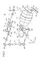
- FIG. 1 is a perspective view showing a schematic configuration of a pattern forming apparatus (pattern drawing apparatus) EX that exposes a pattern to a substrate (irradiated body) P as a substrate processing apparatus according to the first embodiment.
- a pattern forming apparatus pattern drawing apparatus
- EX that exposes a pattern to a substrate (irradiated body) P as a substrate processing apparatus according to the first embodiment.
- International Publication No. 2017/191777 International Publication No. 2018/061633.
- an XYZ Cartesian coordinate system with the gravity direction as the Z direction is set, and the X direction, the Y direction, and the Z direction are set according to the arrows shown in the figure.
- the pattern drawing device EX is used in a device manufacturing system that manufactures an electronic device by exposing a fine pattern for an electronic device to a photosensitive functional layer such as a photoresist coated on the substrate P.
- a photosensitive functional layer such as a photoresist coated on the substrate P.
- the substrate P is delivered from a supply roll (not shown) in which a flexible sheet-shaped substrate (sheet substrate) P is wound in a roll shape, and various processes are continuously performed on the sent substrate P.
- the substrate P has a so-called roll-to-roll (Roll To Roll) production method in which the substrate P after various treatments is wound up with a recovery roll (not shown). Therefore, at least on the substrate P being manufactured, a large number of patterns corresponding to the unit device (one display panel, etc.) to be the final product are arranged in a continuous state with a predetermined gap in the transport direction of the substrate P. Will be done.
- the substrate P has a strip shape in which the elongated direction is the moving direction (transporting direction) of the substrate P and the short direction orthogonal to the elongated direction is the width direction of the substrate P.
- the substrate P for example, a resin film, a foil made of a metal such as stainless steel, or a foil made of an alloy is used.
- the material of the resin film include polyethylene resin, polypropylene resin, polyester resin, ethylene vinyl copolymer resin, polyvinyl chloride resin, cellulose resin, polyamide resin, polyimide resin, polycarbonate resin, polystyrene resin, and vinyl acetate resin. Of these, those containing at least one may be used.
- the thickness and rigidity (Young's modulus) of the substrate P are within a range in which the substrate P does not have creases or irreversible wrinkles due to buckling when passing through the transport path of the device manufacturing system or the pattern drawing device EX. It should be.
- a film such as PET (polyethylene terephthalate), PEN (polyethylene naphthalate), or polyimide having a thickness of about 25 ⁇ m to 200 ⁇ m as a base material of the substrate P is typical of a suitable sheet substrate.
- the substrate P is a single layer of ultrathin glass having a thickness of about 30 to 100 ⁇ m manufactured by a float method or the like, a laminate obtained by laminating the above resin film, metal foil, or the like on the ultrathin glass, or A piece of paper containing nanocellulose and having its surface smoothed may be used.
- the photosensitive functional layer applied to the surface of the substrate P is applied as a solution on the substrate P and dried to become a layer (film).
- a typical photosensitive functional layer is a photoresist (liquid or dry film), but as a material that does not require development processing, the photosensitive functional layer is modified in terms of the liquid repellency of the portion exposed to ultraviolet rays.
- SAM silane coupling agent
- a photosensitive reducing agent that exposes a plating-reducing group to a portion irradiated with ultraviolet rays and a photosensitive reducing agent that removes a plating-reducing group from a portion irradiated with ultraviolet rays.
- the pattern portion exposed to ultraviolet rays on the substrate P is modified from liquid repellent to liquid repellent. Therefore, by selectively coating a conductive ink (ink containing conductive nanoparticles such as silver and copper) or a liquid containing a semiconductor material on the portion that has become liquid-friendly, a thin film transistor (TFT) or the like can be selected. It is possible to form a pattern layer as a wiring for electrodes, semiconductors, insulation, or connections constituting the above.
- the plating reducing group is exposed on the pattern portion exposed to ultraviolet rays on the substrate P or the unexposed pattern portion. Therefore, after exposure, the pattern layer is formed (precipitated) by electroless plating in which the substrate P is immediately immersed in a plating solution containing palladium ions, copper ions, or the like for a certain period of time.
- a plating process is an additive (addition type) process, but in addition, an etching process as a subtractive (subtraction type) process may be premised.
- the substrate P sent to the pattern drawing apparatus EX has a base material of PET or PEN, and a metallic thin film such as aluminum (Al) or copper (Cu) is deposited on the entire surface thereof or selectively, and the substrate P is further deposited. It is assumed that a photoresist layer is laminated on top.
- the pattern drawing device EX shown in FIG. 1 is a direct drawing type exposure device that does not use a mask, a so-called spot scanning type exposure device, and the substrate P conveyed from the process device in the previous process is used as a process device in the subsequent process. Transport in the elongated direction at a predetermined speed toward (including a single processing unit or a plurality of processing units).
- the pattern drawing device EX has one of a signal line constituting an electronic device, a wiring pattern of a power supply line, an electrode constituting a TFT, a semiconductor region, a through hole, etc. in the photosensitive functional layer of the substrate P.
- An optical pattern corresponding to the pattern shape of the above is formed by high-speed scanning in the Y direction (main scanning) of spot light whose intensity is modulated according to drawing data and movement of the substrate P in the long direction (secondary scanning). ..
- the pattern drawing device EX has a pattern for each portion of a rotary drum DR that supports a substrate P for subscanning and conveys it in a long direction, and a portion of the substrate P that is supported in a cylindrical surface by the rotary drum DR.
- a plurality of (here, 6) drawing units Un (U1 to U6) for exposure are provided, and each of the plurality of drawing units Un (U1 to U6) is a pulsed beam LB (pulse beam) for exposure.
- LB pulsed beam
- the substrate P is continuously conveyed along the elongated direction, the exposed region (device forming region) on the substrate P on which the pattern is exposed by the pattern drawing device EX is in the elongated direction of the substrate P.
- a plurality of can be set with a predetermined interval (margin) along the line.
- the pattern forming mechanism is configured by each or all of the six drawing units U1 to U6.
- the rotary drum DR has a central axis AXo extending in the Y direction and extending in a direction intersecting the direction in which gravity acts, and a cylindrical outer peripheral surface having a constant radius from the central axis AXo.
- the rotary drum DR rotates around the central axis AXo while supporting (holding close contact) a part of the substrate P by bending it in a cylindrical surface shape in the elongated direction following its outer peripheral surface (circumferential surface).
- the substrate P is conveyed in the long direction.
- the rotary drum DR supports a region (part) on the substrate P on which the beam LB (spot light) from each of the plurality of drawing units Un (U1 to U6) is projected by its outer peripheral surface.
- a rotational drive source for example, a motor, a deceleration mechanism, etc.
- a rotational torque from a rotational drive source (for example, a motor, a deceleration mechanism, etc.) (not shown) is applied to the shaft, and the rotary drum DR rotates at a constant rotational speed around the central axis AXo.
- the light source device (pulse light source device) LS generates and emits a pulsed beam (pulse beam, pulse light, laser) LB.
- This beam LB has sensitivity to the photosensitive functional layer of the substrate P, and has a peak wavelength (for example, a center wavelength of 405 nm, 365 nm, 355 nm, 344 nm, 308 nm, 248 nm, etc.) in the wavelength band of 410 to 200 nm. It is the ultraviolet light that it has.
- the light source device LS emits a pulsed beam LB at an FPL having a frequency (oscillation frequency, predetermined frequency) in the range of, for example, 100 MHz to 400 MHz, according to the control of a drawing control device (not shown here).
- the light source device LS is a laser light source device that generates ultraviolet light by a wavelength conversion element.
- a semiconductor laser element that generates pulsed light in the infrared wavelength range
- a fiber amplifier that converts the amplified pulsed light in the infrared wavelength range into pulsed light in the ultraviolet wavelength range
- a fiber amplifier laser light source composed of a generating element) or the like.
- the light source device LS is used as a fiber amplifier laser light source, and the pulse generation of the beam LB is turned on / off at high speed according to the state of the pixel bits (logical value "0" or "1") constituting the drawing data (spot light).
- the (intensity-modulated) configuration is disclosed in International Publication No. 2015/166910 and International Publication No. 2017/057415. It is assumed that the beam LB emitted from the light source device LS has a thin parallel luminous flux having a beam diameter of about 1 mm or about half of the beam diameter.
- the beam LB emitted from the light source device LS includes a selection optical element OSn (OS1 to OS6) as a plurality of switching elements, a plurality of reflection mirrors M1 to M12, and a plurality of epi-illumination mirrors (also referred to as selection mirrors) Imn (also referred to as a selection mirror). It is selectively (alternatively) supplied to each of the drawing units Un (U1 to U6) via the beam switching unit composed of the IM1 to IM6) and the absorber TR or the like.
- the selective optical elements OSn (OS1 to OS6) have transparency with respect to the beam LB, and are driven by an ultrasonic signal to efficiently generate only one of the ⁇ 1st-order diffracted light of the incident beam LB.
- the plurality of selection optical elements OSn and the plurality of epi-illumination mirrors Imn are provided corresponding to each of the plurality of drawing units Un.
- the selection optical elements OS1 and the epi-illumination mirror IM1 are provided corresponding to the drawing unit U1
- the selection optical elements OS2 to OS6 and the epi-illumination mirrors IM2 to IM6 correspond to the drawing units U2 to U6, respectively. It is provided.
- the optical path of the beam LB from the light source device LS is bent in a zigzag shape in a plane parallel to the XY plane by the reflection mirrors M1 to M12, and is guided to the absorber TR.
- the selection optical elements OSn OS1 to OS6
- a relay system using a plurality of lenses is provided in the beam optical path from the reflection mirror M1 to the absorber TR.
- the relay system is specifically arranged between the selection optical elements OS1 to OS6 arranged in series along the optical path of the beam LB from the light source device LS, as disclosed in International Publication No.
- Each of the six selection optical elements OS1 to OS6 is optically coupled to each other (imaging relationship). Further, each relay system maintains the diameter of the beam LB as a thin parallel luminous flux of 1 mm to 0.5 mm at each position of the six selection optical elements OS1 to OS6, while the diameter is 0 at the intermediate position in each relay system. Converge so that the beam waist is 2 mm or less. Each of the epi-illumination mirrors IM1 to IM6 is arranged at the position of the beam waist in the optical path of each relay system.
- the beam LB from the light source device LS travels in the ⁇ X direction, is reflected by the reflection mirror M1 in the ⁇ Y direction, and is incident on the reflection mirror M2.
- the beam LB reflected in the + X direction by the reflection mirror M2 passes straight through the selection optical element OS 5 and reaches the reflection mirror M3.
- the beam LB reflected in the ⁇ Y direction by the reflection mirror M3 is reflected in the ⁇ X direction by the reflection mirror M4, passes straight through the selection optical element OS6, and reaches the reflection mirror M5.
- the beam LB reflected in the ⁇ Y direction by the reflection mirror M5 reaches the reflection mirror M6.
- the beam LB reflected in the + X direction by the reflection mirror M6 passes straight through the selection optical element OS3 and reaches the reflection mirror M7.
- the beam LB reflected in the ⁇ Y direction by the reflection mirror M7 is reflected in the ⁇ X direction by the reflection mirror M8, and then passes straight through the selection optical element OS4 to reach the reflection mirror M9.
- the beam LB reflected in the ⁇ Y direction by the reflection mirror M9 is reflected in the + X direction by the reflection mirror M10, and then passes straight through the selection optical element OS1 to reach the reflection mirror M11.
- the beam LB reflected in the ⁇ Y direction by the reflection mirror M11 is reflected in the ⁇ X direction by the reflection mirror M12, and then passes straight through the selection optical element OS2 and is guided to the absorber TR.
- This absorber TR is an optical trap that absorbs the beam LB in order to suppress leakage of the beam LB to the outside, and is provided with a temperature control (air cooling or water cooling) mechanism so as to reduce heat generation due to absorption of light energy. ing.
- each selection optical element OSn When an ultrasonic signal (high frequency signal) is applied, each selection optical element OSn emits first-order diffracted light obtained by diffracting an incident beam LB (0th-order light) at a diffraction angle corresponding to a high-frequency frequency. It is generated as (beam LBn). Therefore, the beam emitted as the primary diffracted light from the selection optical element OS1 becomes LB1, and similarly, the beam emitted as the primary diffracted light from each of the selection optical elements OS2 to OS6 becomes LB2 to LB6. As described above, each selection optical element OSn (OS1 to OS6) functions to deflect the optical path of the beam LB from the light source device LS.
- only one of the selection optical elements OSn (OS1 to OS6) is turned on for a certain period of time (a state in which a high frequency signal is applied), which is not shown. It is controlled by the drawing control device.
- one selected optical element OSn for selection is in the ON state, about 10 to 20% of 0th-order light that travels straight without being diffracted by the optical element OSn for selection remains, which is finally due to the absorber TR. Be absorbed.
- Each of the selection optical elements OSn is installed so as to deflect the deflected primary diffracted light beam LBn (LB1 to LB6) in the ⁇ Z direction with respect to the traveling direction of the incident beam LB.
- the beam LBn (LB1 to LB6) deflected and emitted by each of the selection optical elements OSn is an epi-illumination mirror Imn (position of the beam waist) provided at a position (beam waist position) separated from each of the selection optical elements OSn by a predetermined distance. It is projected on IM1 to IM6).
- Each epi-mirror Imn reflects the incident beam LBn (LB1 to LB6) in the ⁇ Z direction to guide the beam LBn (LB1 to LB6) to the corresponding drawing units Un (U1 to U6).
- each selection optical element OSn The configuration, function, operation, etc. of each selection optical element OSn are the same as each other, and each of the plurality of selection optical elements OSn is incident by turning on / off the drive signal (high frequency signal) from the drawing control device.
- a switching (beam selection) operation is performed to turn on / off the generation of diffracted light (beams LB1 to LB6) diffracted by the beam LB.
- the beam LB from the light source device LS can be guided to any one drawing unit Un, and the drawing unit Un on which the beam LBn is incident can be switched. ..
- each of the selection optical elements OSn (OS1 to OS6) constituting the beam switching unit is turned on for a certain period of time. Determined by order.
- one of the drawing units U1 to U6 is synchronized by synchronizing the rotation speeds of the polygon mirrors PM provided in each of the six drawing units U1 to U6 and also synchronizing the phases of the rotation angles.
- One reflective surface of the polygon mirror in the above can be switched to time division so as to perform one spot scan on the substrate P.
- the order of spot scanning of the drawing unit Un may be any order as long as the phases of the rotation angles of the polygon mirrors of the drawing unit Un are synchronized in a predetermined relationship.
- three drawing units U1, U3, and U5 are arranged side by side in the Y direction on the upstream side of the substrate P in the transport direction (the direction in which the outer peripheral surface of the rotating drum DR moves in the circumferential direction), and the substrate P is arranged.
- Three drawing units U2, U4, and U6 are arranged side by side in the Y direction on the downstream side in the transport direction.
- the pattern drawing for one exposed area on the substrate P is started from the odd-numbered drawing units U1, U3, and U5 on the upstream side, and when the substrate P is sent for a certain length, the even-numbered drawing on the downstream side is drawn. Since the units U2, U4, and U6 also start pattern drawing, the order of spot scanning of the drawing unit Un can be set to U1 ⁇ U3 ⁇ U5 ⁇ U2 ⁇ U4 ⁇ U6 ⁇ U1 ⁇ ... .. Therefore, the order in which each of the selection optical elements OSn (OS1 to OS6) is turned on for a certain period of time is also determined in the order of OS1 ⁇ OS3 ⁇ OS5 ⁇ OS2 ⁇ OS4 ⁇ OS6 ⁇ OS1 ⁇ ....
- each of the drawing units U1 to U6 is provided with a polygon mirror PM for main scanning the incident beams LB1 to LB6.
- each of the polygon mirror PMs of each drawing unit Un is synchronously controlled so as to maintain a constant rotation angle phase with each other while precisely rotating at the same rotation speed.
- the timings of the main scans of the beams LB1 to LB6 projected from each of the drawing units U1 to U6 onto the substrate P (main scan period of the spot light) can be set so as not to overlap each other.
- the light source device by controlling the on / off switching of each of the selection optical elements OSn (OS1 to OS6) provided in the beam switching unit in synchronization with the rotation angle position of each of the six polygon mirror PMs, the light source device. Efficient exposure processing can be performed by distributing the beam LB from the LS to each of the plurality of drawing units Un in a time-division manner.
- the synchronization control between the phase matching of each rotation angle of the six polygon mirror PMs and the on / off switching timing of each of the selection optical elements OSn (OS1 to OS6) is also disclosed in International Publication No. 2015/166910. ing.
- the pattern drawing apparatus EX is a so-called multi-head type direct drawing exposure method in which a plurality of drawing units Un (U1 to U6) having the same configuration are arranged.
- Each of the drawing units Un draws a pattern for each partial region partitioned in the Y direction (main scanning direction) of the substrate P supported by the outer peripheral surface (circumferential surface) of the rotating drum DR.
- Each drawing unit Un (U1 to U6) focuses (converges) the beam LBn on the substrate P while projecting the beam LBn from the beam switching unit onto the substrate P (on the irradiated surface of the substrate P).
- the beam LBn (LB1 to LB6) projected on the substrate P becomes spot light having a diameter of 2 to 4 ⁇ m.
- each spot light of the beam LBn (LB1 to LB6) projected on the substrate P is scanned in the main scanning direction (Y direction).
- the drawing line SLn is a scanning locus of the spot light of the beam LBn on the substrate P.
- the odd-numbered drawing lines SL1, SL3, and SL5 are located on the irradiated surface of the substrate P on the upstream side (-X direction side) of the substrate P in the transport direction with respect to the central surface. Moreover, they are arranged in a row at predetermined intervals along the Y direction.
- the even-numbered drawing lines SL2, SL4, and SL6 are located on the irradiated surface of the substrate P on the downstream side (+ X direction side) of the substrate P in the transport direction with respect to the central surface, and are predetermined along the Y direction. They are arranged in a row at intervals of. Therefore, the odd-numbered drawing units U1, U3, and U5 and the even-numbered drawing units U2, U4, and U6 are provided symmetrically with respect to the central plane when viewed in the XZ plane (when viewed from the Y direction). There is.
- the odd-numbered drawing lines SL1, SL3, SL5 and the even-numbered drawing lines SL2, SL4, SL6 are separated from each other, but in the Y direction (width direction of the substrate P).
- Main scanning direction the patterns drawn on the substrate P are set so as to be spliced together without being separated from each other.
- the drawing lines SL1 to SL6 are set so as to be substantially parallel to the width direction of the substrate P, that is, the central axis AXo of the rotating drum DR.
- joining the drawing lines SLn in the Y direction means that the positions of the ends of the drawing lines SLn in the Y direction are adjacent to each other or partially overlapped with each other.
- the drawing start point or the drawing end point is included in the range of 1 to 5% in the Y direction. It is good to duplicate.
- the plurality of drawing units Un share a scanning area (main scanning range section) in the Y direction so as to cover the widthwise dimension of the exposed area (pattern forming area) on the substrate P in total. doing.
- the main scanning range (the length of the drawing line SLn) in the Y direction by one drawing unit Un is about 30 to 60 mm
- drawing is possible by arranging the six drawing units U1 to U6 in the Y direction.
- the width of the exposed area in the Y direction is widened to about 180 to 360 mm.
- the length (length of the drawing range) of each drawing line SLn (SL1 to SL6) is the same in principle. That is, in principle, the scanning distances of the spot light SPs of the beams LBn scanned along each of the drawing lines SL1 to SL6 are the same.
- Each drawing unit Un includes a telecentric f ⁇ lens system (scanning optical system for drawing) FT that incidents a beam LBn that is reflected by each reflecting surface RP of the polygon mirror PM and deflected in the main scanning direction.
- Each beam LBn emitted from the f ⁇ lens system FT and projected onto the substrate P is set to travel toward the central axis AXo of the rotating drum DR when viewed in the XZ plane.
- the main ray of the beam LBn traveling from each drawing unit Un (U1 to U6) toward the substrate P is directed to the tangent plane at the position of the drawing line SLn on the curved surface of the substrate P in the XZ plane.
- the beams LBn (LB1 to LB6) projected on the substrate P are scanned in a telecentric state with respect to the main scanning direction and the sub-scanning direction (circumferential direction along the outer peripheral surface of the rotating drum DR) of the spot light SP. ..
- FIG. 2 shows the arrangement of the rotary drum DR of the pattern drawing device EX and the six drawing units U1 to U6 shown in FIG. 1, the alignment mark formed on the substrate P, the reference pattern formed on the surface of the rotary drum DR, and the like. It is a figure which concretely showed the arrangement of a plurality of alignment systems ALGn (n is an integer of 2 or more) which detects, and the setting of the orthogonal coordinate system XYZ in FIG. 2 is the same as FIG.
- the basic arrangement of the rotary drum DR, the drawing units U1 to U6, and the alignment system ALGn shown in FIG. 2 is disclosed in, for example, International Publication No. 2016/152758 and International Publication No. 2017/199658.
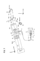
- the drawing unit U1 in a plane parallel to the XZ plane of the Cartesian coordinate system XYZ, the drawing unit U1 (and U3, U5) is tilted counterclockwise by a certain angle ⁇ c from the central plane CPo, and the drawing unit U2 (and U3, U5) And U4, U6) are tilted clockwise from the central surface CPo by a certain angle ⁇ c. Since the configurations of the drawing units U1 to U6 are the same, the configuration of the drawing unit U1 is shown in FIG. 3 as a representative.
- the beam LB1 (parallel light flux having a diameter of about 0.5 mm whose intensity is modulated according to the drawing data) supplied from the epi-illumination mirror IM1 shown in FIG. 1 is finally used as a spot light SP on the substrate P.
- the Cartesian coordinate system XtYtZt tilted with respect to the Cartesian coordinate system XYZ is set.
- the Yt direction is the same as the Y direction
- the Zt direction is the traveling direction of the main ray (center ray) of the beam LB1 incident on the drawing unit U1 from the epi-illumination mirror IM1, or the position of the drawing line SL1.
- the Xt direction is the direction of the optical axis AXf1 passing through the f ⁇ lens system FT.
- the optical axis of each f ⁇ lens system FT of the even-numbered drawing units U2, U4, and U6 is the optical axis AXf2.
- a mirror M30 In the drawing unit U1 (and U2 to U6), a mirror M30, a lens L6, a lens L7, a tiltable parallel flat plate HVP made of quartz, lenses L8, L9, a mirror M31, a polarizing beam splitter PBS, and an opening.
- Aperture AP 1/4 wavelength plate QW, mirror M32, first cylindrical lens CYa, lens L10, mirror M33, lens L11, mirror M34, M35, M36, 8-sided polygon mirror PM, f ⁇ lens system FT, mirror M37,
- the second cylindrical lens CYb is arranged in that order.
- the mirror M30 reflects the beam LB1 at 90 degrees so that the traveling direction of the incident beam LB1 is in the ⁇ Xt direction.
- the lenses L6, L7, L8, and L9 arranged along the optical path of the beam LB1 reflected by the mirror M30 have a thin beam LB1 (diameter of about 0.5 mm) reflected by the mirror M30 of several mm or more (5). It constitutes a beam expander system that expands to a parallel light flux with a diameter (in the range of ⁇ 10 mm).
- the parallel flat plate HVP is provided in the optical path between the lenses L6 to L9 of the beam expander system, and is configured to be rotatable (tilted) around the rotation axis AXh parallel to the Zt axis.
- the position of the spot light SP projected on the substrate P can be effectively changed to the sub-scanning direction (Xt direction, the sub-scanning direction which is the moving direction of the substrate P). It can be shifted in a distance range of several times to ten and several times the diameter ⁇ p.
- the polarization beam splitter PBS incident on the beam LB1 (parallel luminous flux) which is magnified through the lens L9 and reflected by the mirror M31 in the ⁇ Yt direction.
- the polarization beam splitter PBS reflects the beam LB1 at the polarization separation surface with an intensity of 90% or more and directs the beam LB1 to the aperture stop AP in the subsequent stage.
- the beam LB transmitted through the circular aperture of the aperture stop AP is converted from linearly polarized light to circularly polarized light when transmitted through the 1/4 wave plate QW.
- the beam LB1 (parallel luminous flux) transmitted through the 1/4 wave plate QW is reflected in the ⁇ Zt direction by the mirror M32, is incident on the first cylindrical lens CYa (the bus is parallel to the Yt axis), and is formed on the surface Pv in space.
- the width in the Xt direction is extremely small, and the light is focused on a slit-shaped intensity distribution extending in the Yt direction with a length of several mm (same as the opening diameter of the aperture throttle AP).
- the beam LB1 converged only in the one-dimensional direction by the surface Pv passes through the spherical lens L10 of the first group of the two-disc spherical lens system, is reflected by the mirror M33 in the + Xt direction, and then is reflected in the + Xt direction, and then the two-disc spherical lens system. It advances in the + Xt direction through the spherical lens L11 in the rear group.
- the beam LB1 after being emitted from the spherical lens L11 is reflected in the + Zt direction by the mirror M34 and then reflected in the + Yt direction by the mirror M35.
- the mirror M34 and the mirror M35 are arranged so that the main ray (center ray) of the beam LB1 traveling in the + Yt direction from the mirror M35 and the optical axis AXf1 of the f ⁇ lens system FT are orthogonal to each other in a plane parallel to the XtYt plane. There is.
- the beam LB1 traveling in the + Yt direction from the mirror M35 is reflected by the mirror M36 arranged on the opposite side of the mirror M35 with the optical axis AXf1 of the f ⁇ lens system FT interposed therebetween, and is projected onto the reflection surface RPa of the polygon mirror PM.
- the beam LB1 incident on the mirror M34 immediately after passing through the spherical lens L11 becomes a state of almost parallel light beam in the Zt direction and converges in the Yt direction. It becomes a state of light beam.
- the spherical lens system is composed of two spherical lenses L10 and L11 for adjusting the distance between the principal points, but it may be composed of only one spherical lens.
- the reflective surface of the mirror M36 is arranged at a narrow angle of 22.5 ° with respect to the surface including the optical axis AXf1 which is parallel to the Zt axis and parallel to the XtZt surface.
- the main ray (center ray) of the beam LB1 directed from the mirror M36 toward the reflection surface RPa of the polygon mirror PM, that is, the extension of the optical axis of the first cylindrical lens CYa and the spherical lens system (lenses L10, L11), the mirror M36.
- the optical axis from to the polygon mirror PM is set at an angle of 45 ° with respect to the optical axis AXf1 of the f ⁇ lens system FT in a plane parallel to the XtYt plane. Further, in FIG. 3, the beam LB1 reflected by the mirror M36 and directed toward the reflecting surface RPa of the polygon mirror PM is in a convergent light beam state so as to be focused on the reflecting surface RPa of the polygon mirror PM in the Zt direction, and is in the state of XtYt.
- the intensity distribution extends in a slit shape in the main scanning direction, that is, in the tangential direction of the inscribed circle centered on the rotation center axis AXp of the polygon mirror PM. It is condensed so as to be.
- the beam LB1 reflected by the reflecting surface RPa of the polygon mirror PM is reflected by the mirror M37 at a right angle in the ⁇ Zt direction after passing through the telecentric f ⁇ lens system FT, and is reflected by the second cylindrical lens CYb (the direction of the bus is Yt). It is incident on the substrate P and is focused as a spot light SP on the substrate P.
- the optical axis AXf1 of the f ⁇ lens system FT which is bent at a right angle in the ⁇ Zt direction by the mirror M37 and becomes perpendicular to the surface of the substrate P (the outer peripheral surface of the rotating drum DR), and toward the mirror M30.
- the central ray of the beam LB1 incident in the ⁇ Zt direction is set to be coaxial with the line segment LE1 parallel to the Zt axis (the line segments LE2 to LE6 are used for each of the other drawing units U2 to U6). ing.
- the drawing line SL1 is tilted by a small amount in the substrate P (plane parallel to the XtYt plane)
- each optical member from the mirror M30 to the second cylindrical lens CYb shown in FIG. 3 is integrated.
- the entire supporting housing (unit support frame) can be slightly rotated around the line segment LE1.
- the intensity of the reflected light generated when the spot light SP is projected onto the surface of the irradiated object (the substrate P or the outer peripheral surface of the rotating drum DR) installed on the scanned surface is detected. Therefore, a photoelectric sensor DTR and a lens system GF are provided.
- the reflected light (particularly normal reflected light) from the surface of the irradiated body is the second cylindrical lens CYb, the f ⁇ lens system FT, the reflecting surface RPa of the polygon mirror PM, the mirrors M36, M35, M34, the spherical lens L11, and the mirror M33.
- the polarizing beam splitter PBS It returns to the polarizing beam splitter PBS via the spherical lens L10, the first cylindrical lens CYa, the mirror M32, the 1/4 wavelength plate QW, and the aperture aperture AP. Since the spot light SP projected on the surface of the irradiated object is circularly polarized light and the reflected light also contains a large amount of circularly polarized light components, the reflected light passes through the 1/4 wave plate QW and becomes the polarized beam splitter PBS. When heading, its polarization characteristics are converted to linear P-polarized light. Therefore, the reflected light from the surface of the irradiated body passes through the polarization splitting surface of the polarizing beam splitter PBS and is incident on the lens system GF.
- the light receiving surface of the photoelectric sensor DTR is set to be optically coupled to the spot light SP on the scanned surface so that the reflected light from the irradiated body is focused on the light receiving surface of the photoelectric sensor DTR by the lens system GF. Will be done.
- the reflective surface of the polygon mirror PM on which the beam LB1 for drawing is projected is disclosed in International Publication No. 2015/166910 or International Publication No. 2016/152758.
- a pulse-shaped origin signal indicating that each reflective surface of the polygon mirror PM is at the angular position immediately before the start of drawing is sent to the reflective surface RPb immediately before the rotation direction of RPa for the origin sensor.
- a light beam is projected.
- the detailed internal configuration of the drawing unit U1 shown in FIG. 3 is the same for the other drawing units U2 to U6, but each of the even-numbered drawing units U2, U4, and U6 is the drawing unit U1 of FIG. Is installed in a direction rotated by 180 degrees around the line segment LE1.
- the configuration of the pattern drawing apparatus EX will be further described with reference to FIG. 2 again.
- the extension lines of the line segments LE1, LE3, and LE5 that is, the extension lines of the optical axis AXf1 of the f ⁇ lens system FT
- the line segments LE1, LE3, and LE5 are installed so as to be tilted counterclockwise by an angle ⁇ c with respect to the central surface CPo while facing the rotation center axis AXo of the rotating drum DR when viewed from the Y direction of 2.
- the extension lines of the line segments LE2, LE4, and LE6 (that is, the extension lines of the optical axis AXf2 of the f ⁇ lens system FT) are viewed from the Y direction in FIG.
- the line segments LE2, LE4, and LE6 are installed so as to be tilted clockwise by an angle + ⁇ c with respect to the center surface CPo while facing the rotation center axis AXo of the rotation drum DR.
- the angle ⁇ ⁇ c is set to be as small as possible within a range in which the odd-numbered drawing units U1, U3, U5 and the even-numbered drawing units U2, U4, and U6 do not spatially interfere with each other (do not collide).
- a plurality of alignment systems ALGn are arranged in the Y direction at predetermined intervals, and each includes an objective lens system (objective optical system) for detecting a mark or the like on the substrate P.
- the detection region (observation field of view) set on the substrate P via the objective lens system is drawn by each of the drawing units U1 to U6 with respect to the moving direction of the substrate P (circumferential direction of the outer peripheral surface of the rotating drum DR). It is arranged on the upstream side of the positions of lines SL1 to SL6.
- each optical axis AXs of the objective lens system passing through the center of the detection region (observation field) is directed toward the rotation center axis AXo of the rotating drum DR, and the surface of the substrate P is located at the position of the detection area (observation field). Alternatively, it is set to be perpendicular to the outer peripheral surface of the rotating drum DR.
- a reference bar member RB as a reference index member forming a reference mark (reference index mark) is attached near the tip of the alignment system ALGn.
- the reference mark of the reference bar member RB calibrates the mutual positional relationship of the detection areas (observation fields of view) by each of the objective lens systems, or the mutual positional relationship of the drawing lines SL1 to SL6 by each of the drawing units U1 to U6. It is also used when measuring the interval (baseline length) and positional relationship in the circumferential direction (moving direction of the substrate P) between the positions of the drawing lines SL1 to SL6 and each position of the plurality of detection areas.
- each optical axis AXs of the alignment system ALGn has an angle ⁇ a larger than the angle ⁇ c of the drawing lines SL1, SL3, SL5 by each of the odd-numbered drawing units U1, U3, U5. Only the central surface CPo is set to tilt counterclockwise.
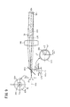
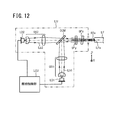
- FIG. 4 is a perspective view showing the arrangement relationship between the rotary drum DR shown in FIG. 2, the alignment system ALGn, and the reference bar member RB, and the quadrature coordinate system XYZ is the same as the quadrature coordinate system XYZ of FIG. Set to the same.
- seven alignment systems ALG1 to ALG7 (collectively referred to as ALGn) having the same configuration are linearly arranged in the Y direction at predetermined intervals.
- the optical axis AXs of the objective lens system (objective optical system) OBL of the alignment system ALGn is bent by a plane mirror Mb arranged between the objective lens system OBL and the substrate P (outer peripheral surface DRs of the rotating drum DR), and the substrate is bent.
- a plate-type beam splitter BS1 synthetic optical member inclined with respect to a plane perpendicular to the optical axis AXs is provided in the optical path between the objective lens system OBL and the plane mirror Mb.
- the alignment system ALGn further includes an optical splitter (beam splitter) BS2 for incidentally incident the illumination light ILb supplied from the optical fiber bundle ILF on the objective lens system OBL to epiilluminate the detection region ADn, and the objective lens system OBL. And the reflected light from the detection region ADn incident via the optical divider BS2 is received via the imaging lens system Gb, and an enlarged image of the alignment mark (board mark) on the substrate P that appears in the detection region ADn. It has an image pickup unit (imaging element) DIS that captures an image.
- imaging element imaging element
- FIG. 4 shows the configuration of the alignment system ALG1 and ALG2 only by the plane mirror Mb, the beam splitter BS1, the objective lens system OBL, the optical splitter BS2, the imaging lens system Gb, and the image pickup unit (imaging element) DIS.
- Each of the other alignment systems ALG3 to ALG7 has the same configuration, and the optical axes AXs of each of the alignment systems ALG3 to ALG7 are also set in the detection regions AD3 to AD7 (not shown in FIG. 4). (Omitted) is set to pass through the center point.
- FIG. 4 six drawing lines SL1 to SL6 are set on the substrate P.
- the odd-numbered drawing lines SL1, SL3, and SL5 are arranged on the downstream side of the detection region ADn of the alignment system ALGn with respect to the transport direction (sub-scanning direction) of the substrate P due to the rotation of the rotating drum DR, and the even-numbered drawing lines SL2.
- SL4, SL6 are arranged on the downstream side of the odd-numbered drawing lines SL1, SL3, SL5.
- the drawing line SL1 draws a pattern in the region between the line OL01 extending in the circumferential direction on the substrate P and the line OL12 in the Y direction, and the drawing line SL2 is drawn with the line OL12 extending in the circumferential direction on the substrate P.
- the pattern is drawn in the area between the line OL23 and the Y direction.
- the line OL12 represents a joint portion (or a portion exposed by partially overlapping) in which the pattern exposed by the drawing line SL1 and the pattern exposed by the drawing line SL2 are joined in the Y direction.
- the line OL23 represents the joint of the pattern exposed by the drawing line SL2 and the drawing line SL3
- the line OL34 is represented by the drawing line SL3 and the drawing line SL4.
- the line OL45 represents the joint of the pattern to be exposed
- the line OL45 represents the joint of the pattern exposed by the drawing line SL4 and the drawing line SL5
- the line OL56 represents the joint of the pattern exposed by the drawing line SL5 and the drawing line SL6. Represents a part.
- the detection area AD1 of the alignment system ALG1 is arranged around the drawing area formed by the drawing line SL1 shifted in the + Y direction from the line OL01, and the detection area AD7 of the alignment system ALG7 is also similarly arranged. It is arranged around the drawing area by the drawing line SL6.
- the detection regions AD2 to AD6 of the other alignment systems ALG2 to ALG6 are arranged on the lines OL12, OL23, OL34, OL45, and OL56, respectively.
- the reference bar member RB is elongated in the Y direction with a material having a low coefficient of thermal expansion (Invar, ceramics, quartz, etc.) and is attached in the vicinity of each beam splitter BS1 of the seven alignment systems ALG1 to ALG7.
- a material having a low coefficient of thermal expansion Invar, ceramics, quartz, etc.
- As the material of the reference bar member RB it is desirable to use ceramics that can be made lighter, and in particular, it is composed of three components: magnesium oxide (MgO), aluminum oxide (Al 2 O 3 ), and silicon dioxide (SiO 2). It is recommended to use aluminum-based ceramics.
- the detection region AR1 is located at a position corresponding to the detection region AD1 (AD2 to AD7) on the substrate P of the alignment system ALG1 (same for ALG2 to ALG7).
- a reference mark (reference pattern) RM1 observable by the objective lens system OBL is formed in the detection region AR1 of the reference surface RBa via the beam splitter BS1.
- detection regions AR2 to AR7 AR3 to AR7 are not shown) that can be observed by the objective lens system OBL via the beam splitters BS1 of each of the other alignment systems ALG2 to ALG7.
- Similar reference marks (reference patterns) RM2 to RM7 are formed in the detection regions AR2 to AR7.
- the image pickup unit DIS enables simultaneous or alternative observation.
- the reference marks (reference index marks) RM1 to RM7 formed on the reference surface RBa of the reference bar member (reference index member) RB correspond to the distance between the detection regions AD1 to AD7 set in the design in the Y direction. It is formed at each of the positions.
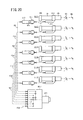
- FIG. 5 shows the arrangement relationship between the drawing lines SL1 to SL6 by each of the drawing units U1 to U6 shown in FIG. 4 and the detection areas AD1 to AD7 of the alignment systems ALG1 to ALG7, and the change in the rotation angle of the rotary drum DR.
- the scale disks SDa and SDb are fixed to each of the shafts Sft at both ends of the rotating drum DR in the Y direction so as to rotate coaxially with the central axis AXo.
- the diameters of the scale disks SDa and SDb are preferably the same as the diameter of the rotating drum DR, but the relative difference between the diameters may be within ⁇ 20%.
- Diffraction grating-like scales Gm engraved at a constant pitch in the circumferential direction are formed on the cylindrical outer peripheral surfaces of the scale disks SDa and SDb.
- the scale Gm may be formed directly on the outer peripheral surfaces of the rotary drum DR on both end sides in the Y direction.
- three optical encoder heads EHa1, EHa2, and EHa3 for measuring the amount of movement of the scale Gm in the circumferential direction are provided side by side in the circumferential direction of the outer peripheral surface of the scale disk SDa, and the scale disk SDb.
- Three optical encoder heads EHb1, EHb2, and EHb3 for measuring the amount of movement of the scale Gm in the circumferential direction are provided side by side in the circumferential direction of the outer peripheral surface of the scale disk SDb.
- the reading position in the circumferential direction of the scale Gm by the pair of encoder heads EHa1 and EHb1 is set to be the same as the angular position in the circumferential direction of each detection area AD1 to AD7 of the alignment systems ALG1 to ALG7 arranged in a row in the Y direction.
- the reading position in the circumferential direction of the scale Gm by the pair of encoder heads EHa2 and EHb2 is set to be the same as the angular position in the circumferential direction of the odd-numbered drawing lines SL1, SL3, and SL5 arranged in a row in the Y direction.
- the reading position of the scale Gm by the pair of encoder heads EHa3 and EHb3 in the circumferential direction is set to be the same as the angular position in the circumferential direction of the even-numbered drawing lines SL2, SL4, and SL6 arranged in a row in the Y direction.
- An encoder measurement system having such an arrangement of encoder heads can minimize the measurement error, as disclosed in, for example, International Publication No. 2013/146184.
- the short length of the substrate P is taken.
- the length LPy is smaller than the dimension in the Y direction of the outer peripheral surface of the rotary drum DR, and is smaller than the dimension in the Y direction of the detection regions AD1 and AD7 of the alignment systems ALG1 and ALG7 set on both ends in the Y direction. Set to be large.
- Alignment marks (board marks) MK1 are arranged in a row at regular intervals (for example, 5 to 20 mm) in the X direction (sub-scanning direction) at the ends in the ⁇ Y direction on the substrate P, and are arranged in the + Y direction on the substrate P.
- Alignment marks MK7 are arranged in a row at regular intervals (for example, 5 to 20 mm) in the X direction (sub-scanning direction) at the ends of the above.
- the alignment mark MK1 is formed at a position where it appears in the detection region AD1 of the alignment system ALG1, and the alignment mark MK7 is formed at a position where it appears in the detection region AD7 of the alignment system ALG7.
- an alignment mark (not shown in FIG. 5, but MK2 to MK6) arranged so as to appear in each of the detection regions AD2 to AD6 of the alignment system ALG2 to ALG6 is also formed on the substrate P.
- the alignment marks MK1 and MK7 on both ends are continuously formed along the long direction on the substrate P, while the other alignment marks MK2 to MK6 are formed at appropriate distances (dimensions) in the long direction. Will be done.
- the linear region formed by each of the drawing lines SL1 to SL6 or the rectangular region surrounded by the entire drawing lines SL1 to SL6 correspond to the pattern forming region.
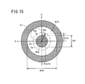
- FIG. 6A is a diagram showing an example of arrangement of reference marks RM1 to RM7 (RM3 to RM6 are omitted) formed at seven locations in the Y direction on the reference surface RB of the reference bar member RB.
- the plane parallel to the reference plane RBa is the X'Y'plane of the Cartesian coordinate system X'Y'Z'
- the axis parallel to the normal of the reference plane RBa is the Z'axis.
- the Y'axis of the Cartesian coordinate system X'Y'Z' is parallel to the Y axis of the Cartesian coordinate system XYZ.
- reference marks RM1 to RM7 are formed at predetermined spacing dimensions in the Y'direction along a virtual straight line CRy extending in the Y'direction (Y direction). .. That is, the center points CR1, CR2, ... CR7 of the reference marks RM1 to RM7 are precisely positioned on the virtual straight line CRy.
- the distance between the center point CR1 of the reference mark RM1 and the center point CR2 of the reference mark RM2 in the Y'direction (Y direction) is set to the dimension LBS12
- the Y'direction between the center point CR3 and the center point CR2 of the reference mark RM3 ( The distance in the Y direction is the dimension LBS23
- the distance between the center point CR4 of the reference mark RM4 and the center point CR3 in the Y'direction (Y direction) is the dimension LBS34
- the distance between the center point CR5 and the center point CR4 of the reference mark RM5 is Y'.
- the distance in the direction (Y direction) is the dimension LBS45
- the distance between the center point CR6 of the reference mark RM6 and the center point CR5 in the Y'direction (Y direction) is the dimension LBS56
- the center point CR7 and the center point CR6 of the reference mark RM7 is the dimension LBS67.
- the dimension LBS12 and the dimension LBS67 are set to the same value
- the dimensions LBS23, LBS34, LBS45, and LBS56 are set to the same value.
- FIG. 6B exaggerates an example of the arrangement relationship between the image pickup region DIS'by the image pickup element DIS of the alignment system ALG1 and the reference mark RM1 on the reference bar member RB in the XY'plane.
- FIG. 6C exaggerates an example of the arrangement relationship between the image pickup region DIS'by the image pickup element DIS of the alignment system ALG2 and the reference mark RM2 on the reference bar member RB in the XY'plane. ..
- the center point (reference point) between the X'direction and the Y'direction of the two-dimensional imaging region DIS'is CC1 the reference is due to the relative mounting error between the reference bar member RB and the alignment system ALG1.
- the installation error ⁇ C1 is + ⁇ XC1 ( ⁇ m) in the X'direction and + ⁇ YC1 ( ⁇ m) in the Y'direction with the center point CR1 of the reference mark RM1 as a reference (origin).
- the installation error ⁇ C2 is ⁇ XC2 ( ⁇ m) in the X'direction and ⁇ YC2 ( ⁇ m) in the Y'direction with respect to the center point CR2 of the reference mark RM2 as a reference (origin).
- the center points CC1 and CC2 of the imaging region DIS' correspond to a specific imaging pixel located in the center of a large number of imaging pixels distributed in a two-dimensional matrix on the imaging surface. It does not have to be exactly the true center point of the imaging region DIS', for example, the position of a specific imaging pixel deviated from the true center point by several to a dozen in the X'direction or Y'direction.
- the center points (reference points) CC1 and CC2 may be used.
- the reference marks RM1 and RM2 are set to appear in an L shape at the four corners in the imaging region DIS', but they are made into a cross-shaped mark shape. It may be set so that it appears in the central portion in the imaging region DIS', or in the portion to the left or right from the center.
- an optical microscope having a working distance (working distance) of 10 cm or more is used as the alignment system ALGn.
- Such a microscope is sold by, for example, Moritex Corporation as a lens for machine vision, and it can also be used.
- the entire alignment system ALGn is fixed to a support bracket (not shown) made of metal or ceramics having a low coefficient of thermal expansion.
- the support bracket is formed in a plate shape parallel to the XZ plane, and is fixed to a structural portion (metrology frame) connected to a device frame portion that supports the drawing units U1 to U6.
- the support bracket has an angle ⁇ e ( ⁇ e> 0) in the XZ plane with respect to the plane perpendicular to the optical axis AXs in the optical path between the plane mirror Mb and the objective lens system OBL, and the plane mirror Mb and the objective lens system OBL.
- Plate-type (parallel flat plate) beam splitter BS1 synthetic optical member made of transmissive optical glass material such as quartz, which is arranged at an angle of only
- an illumination system illumination unit
- the beam splitter BS2 that guides the illumination light ILb from the ILU, the imaging lens system Gb, and the image pickup element DIS are fixed.
- the illumination light ILb for epi-illumination is supplied from the illumination system ILU to the beam splitter BS2 from the emission end ILFb of the optical fiber bundle ILF via the optical fiber bundle (multimode fiber) ILF. ..
- the pupil surface (aperture diaphragm surface) Ep of the objective lens system OBL is formed on the imaging lens system Gb side of the beam splitter BS2, and the objective lens system OBL is also formed on the optical fiber bundle ILF side of the beam splitter BS2.
- a pupil plane (opening diaphragm plane) Ep' is formed.
- the emission end ILFb of the optical fiber bundle ILF is arranged so as to substantially coincide with the pupil surface Ep', and the emission end ILFb becomes a surface light source image of the illumination light ILb that irradiates each detection region ADn or ARn.
- the optical fiber bundle ILF is configured as a light guide member in which a large number of optical fiber strands are bundled, and the surface light source image formed on the emission end ILFb has the shape of the light intensity distribution of the illumination light ILb formed on the incident end ILFa. It will be the one saved.
- the illumination light ILb from the emission end ILFb of the optical fiber bundle ILF is reflected by the beam splitter BS2, enters the objective lens system OBL, passes through the beam splitter BS1, and then is reflected by the plane mirror Mb to be reflected in the detection region on the substrate P. It is projected onto ADn (alignment mark MKn).
- the light reflected by the detection region ADn on the substrate P becomes an imaging light beam (reflected light) Bma via the beam splitter BS1 and the objective lens system OBL, passes through the beam splitter BS2, and passes through the image forming lens system Gb. It leads to the image pickup element DIS.
- the image pickup surface Pis of the image pickup element DIS is set to have an optically conjugate relationship (imaging relationship) with the surface of the detection region ADn on the substrate P, and the reference surface RBa of the reference bar member RB is set via the beam splitter BS1. It is set to an optically conjugate relationship (imaging relationship) with (detection region ARn).
- the intensity of the illumination light ILb emitted from the objective lens system OBL depends on the angle ⁇ e, and the surface of the plate-type beam splitter BS1 (the optical splitting surface). , Photosynthetic surface) Reflected by Bsp and directed toward the reference bar member RB.
- the reference surface RBa of the reference bar member RB is optically set at a position corresponding to the surface of the substrate P, and the detection region ARn set on the reference surface RBa is illuminated with a uniform illuminance distribution by a part of the illumination light ILb. NS.
- the reflected light flux Bm generated at the reference mark RMn arranged in the detection region ARn reaches the beam splitter BS1 along the optical axis AXs', is reflected by the surface Bsp, and is combined with the imaged light beam Bma to be combined with the objective lens system. It is incident on the OBL.
- the plate-type beam splitter BS1 shown in FIG. 7 is a non-polarizing type and may be a glass material other than quartz.
- both the detection region ADn set on the substrate P and the detection region ARn set on the reference bar member RB are simultaneously illuminated by the illumination light ILb. Illuminated by epi-illumination. Therefore, in the image pickup region DIS'of the image pickup element DIS, an image of the alignment mark MKn of the substrate P appearing in the detection region ADn (or an image of the reference pattern on the rotating drum DR) and a reference mark in the detection region ARn. The image of RMn is combined and imaged at the same time.
- the image pickup device DIS outputs a video signal corresponding to each image of the alignment mark MKn and the reference mark RNn to be imaged.
- the emission end ILFb of the optical fiber bundle ILF is set to be located at the position of the pupil surface Ep'of the microscope optical system by the objective lens system OBL, and the emission end ILFb forming a substantially circular outer shape is the pupil.
- Telecentric epi-illumination (Koehler illumination) is performed as a secondary light source image in the surface Ep'.
- the plate-type beam splitter BS1 shown in FIG. 7 above tilts the illumination light ILb emitted from the objective lens system OBL by an angle ⁇ e with respect to the plane perpendicular to the optical axis AXs of the objective lens system OBL, and aligns the illumination light ILb. It was configured to face the reference bar member RB arranged in the space below the ALGn. However, when the reference bar member RB extends in the space above the alignment system ALGn, the inclination of the beam splitter BS1 with respect to the plane perpendicular to the optical axis AXs may be set in the opposite direction ( ⁇ e).
- the thickness of the plate-type beam splitter BS1 should be as thin as possible within a range that reduces the occurrence of various optical aberrations (ass, etc.) and has rigidity that does not cause deformation or distortion that deteriorates surface accuracy. good.
- the light splitting surface (photosynthetic surface) Bsp has an appropriate reflectance depending on the angle ⁇ e. Can be made.
- the angle ⁇ e is determined by the angle 2 ⁇ e (arrangement of the reference bar member RB in the XZ plane) formed by the optical axis AXs and the optical axis AXs', but when the angle ⁇ e becomes, for example, 45 ° or more, the reference bar member Since the intensity of the illumination light ILb toward the RB increases and the intensity of the illumination light ILb toward the substrate P decreases extremely, the angle ⁇ e is in the range of 0 ° ⁇ e ⁇ 45 °, more preferably 5 °. It is better to set it in the range of ⁇ ⁇ e ⁇ 30 °. Further, the thickness of the plate-type beam splitter BS1 may be 1 mm or less, for example, 0.1 mm, and a structure capable of adjusting the angle ⁇ e may be provided.
- the lighting system (lighting unit) ILU shown in FIG. 7 includes a light source unit ILS including a solid-state light source such as an LED or a halogen lamp light source, a lens system GR, and two parallel flat plates SFy and SFz made of a transmissive glass material.
- the lens system GR collects the illumination light ILb from the light source unit ILS so as to have a circular distribution of a predetermined diameter on the circular incident end ILF of the optical fiber bundle ILF.
- the parallel flat plate SFy is provided so as to be tiltable around an axis parallel to the Zt axis in the coordinate system XtYtZt in FIG.
- the parallel flat plate SFz is provided so as to be tiltable around an axis parallel to the Yt axis in the coordinate system XtYtZt in FIG. 7, and positions the illumination light ILb focused on the incident end ILF of the optical fiber bundle ILF in the Zt direction. Adjust the shift.
- the position of the illumination light ILb focused on the incident end ILF is shifted and adjusted to emit light.
- the distribution of the illumination light ILb (circular) formed as a light source image on the end ILFb can be laterally shifted in the pupil plane Ep'(in the plane perpendicular to the optical axis AXs).
- the position of the light source image is changed by the tiltable parallel flat plates SFy and SFz, and the telecentric error of the alignment system ALGn (the tilt error of the optical axis AXs of the objective lens system OBL with respect to the perpendicular line on the surface of the substrate P).
- An adjustment mechanism is configured to compensate for the effects of.
- the inclination of the parallel flat plates SFy and SFz may be adjusted manually or may be electrified by using a small actuator (piezomotor or the like).
- FIG. 8 is a diagram schematically showing the optical arrangement of the objective lens system OBL, the beam splitter BS2, and the exit end ILFb of the optical fiber bundle ILF in FIG. 7, and the planar mirror Mb and the beam splitter BS1 are not shown.
- the optical axis AXs passing through the objective lens system OBL is bent at 90 ° by the beam splitter BS2 and passes through the center of the circular exit end ILFb of the optical fiber bundle ILF.
- the angle formed by the surface of the substrate P (detection region ADn) and the optical axis AXs is relatively slightly tilted from 90 °.
- the maximum diameter of the emission end ILFb of the optical fiber bundle ILF located on the pupil surface Ep'on the illumination system ILU side of the beam splitter BS2 is set to be equal to or slightly smaller than the diameter ⁇ e of the pupil surface Ep'. Then, assuming that the light source image by the illumination light ILb formed on the emission end ILFb is SOb, its diameter ⁇ s is set to about half (40 to 60%) of the maximum diameter of the emission end ILFb.
- the numerical aperture (spread angle) NAi of the illumination light ILb irradiated to the detection region ADn on the substrate P is based on the focal length fob of the objective lens system OBL and the diameter ⁇ s of the light source image SOb of the pupil surface Ep'.
- ⁇ sin ( ⁇ s / 2 / fob).
- the ratio ( ⁇ s / ⁇ e) between the diameter ⁇ e of the pupil surface Ep'and the diameter ⁇ s of the light source image SOb is called the ⁇ value ( ⁇ 1), and the diameter ⁇ s of the light source image SOb is changed, that is, the ⁇ value is changed.
- NAi of the illumination light ILb can be adjusted.
- the main ray of the illumination light ILb emitted from the objective lens system OBL (The light beam generated from the center point on the optical axis AXs of the light source image SOb) reaches the substrate P in parallel with the optical axis AXs.
- the main ray of the reflected light LRf normally reflected in the detection region ADn is also tilted with respect to the optical axis AXs. It is incident on the objective lens system OBL.
- the main ray of the reflected light LRf transmitted through the objective lens system OBL is eccentric from the position on the optical axis AXs in the pupil surface Ep on the image forming lens system Gb side of the beam splitter BS2, for example, in the direction along the Z'axis. Cross (concentrate) at the desired position. Therefore, in the pupil plane Ep, the emission end image ILFb'of the optical fiber bundle ILF and the reflected light source image having a diameter of ⁇ s by the reflected light LRf are eccentric in the + Z'direction from the center point (the intersection of the Y axis and the Z'axis). SOb'is formed.
- the entire reflected light source image SOb' is located in the pupil surface Ep, but scattered light generated from the surface (detection region ADn) of the substrate P is further surrounded around the reflected light source image SOb'. Diffracted light is distributed with a predetermined spread. Due to the telecentric error, a part of the scattered light or diffracted light protrudes from the circular pupil surface Ep, and the symmetry of the image forming luminous flux Bma incident on the image forming lens system Gb is broken, and the image pickup element.
- the image quality of the alignment mark MKn imaged by DIS particularly the edge image of the alignment mark MKn regarding the direction in which the telecentric error occurs, deteriorates. Therefore, an error occurs in the position measurement of the alignment mark MKn by the image analysis based on the video signal.
- the reflected light source image SOb'itself When the telecentric error becomes larger than that in FIG. 8, the reflected light source image SOb'itself also protrudes (is eclipsed) from the circular pupil surface Ep, and the amount of light of the reflected light source image SOb' incident on the imaging lens system Gb. As the (0th-order reflected light amount) decreases, the symmetry of the scattered light and the diffracted light in the pupil surface Ep is significantly broken. Therefore, the brightness of the mark image of the alignment mark MKn imaged by the image sensor DIS is significantly reduced, and the image quality of the mark image is also significantly deteriorated.
- FIG. 9 is a diagram schematically showing the optical arrangement of the objective lens system OBL, the beam splitter BS2, and the emission end ILFb of the optical fiber bundle ILF in FIG. 7 as in FIG. 8. As shown in FIG.
- the center point of the light source image SOb formed on the emission end ILFb of the optical fiber bundle ILF by adjusting the parallel flat plates SFy and SFz (particularly the parallel flat plates SFz) is set in the + Z'direction from the position of the optical axis AXs. Can be shifted to.
- the main ray of the illumination light ILb irradiated from the objective lens system OBL to the detection region ADn on the substrate P is tilted from the state parallel to the optical axis AXs by an angle corresponding to the telecentric error of the alignment system ALGn, and the substrate.
- the main ray of the reflected light LRf from the surface of P can be set parallel to the optical axis AXs. Therefore, in the pupil surface Ep, the emission end image ILFb'of the optical fiber bundle ILF concentrically with the center point (the intersection of the Y axis and the Z'axis) and the reflected light source image SOb' with a diameter of ⁇ s by the reflected light LRf. Is formed.
- the symmetry of the image pickup beam Bma incident on the image pickup lens system Gb is maintained, and deterioration of the image quality (edge image) of the alignment mark MKn imaged by the image pickup element DIS can be prevented.
- the position of the light source image SOb formed on the emission end ILFb of the optical fiber bundle ILF is set independently in the pupil plane Ep'in the Y-axis direction and the Z'-axis direction. Since it can be adjusted, it can handle two-dimensional (Y-axis direction and Z'axis direction) telesen error.
- the influence of the telecentric error of the alignment system ALGn is corrected by adjusting the inclination of the parallel flat plates SFy and SFz, but when the parallel flat plates SFy and SFz are not provided, the figure is shown in the figure.
- the lens system GR in 7 may be tiltable, and the relative positional relationship between the illumination system ILU and the incident end ILF of the optical fiber bundle ILF may be physically adjusted in the Y-axis direction or the Z'axis direction.
- a mechanism fine movement mechanism
- an adjustment mechanism fine movement mechanism for finely moving the emission end ILFb of the optical fiber bundle ILF to the beam splitter BS2 in two dimensions along the pupil plane Ep'may be provided.
- the alignment system ALGn is assembled by laterally shifting (eccentricity) the position of the light source image formed on the pupil surface Ep'of the objective lens system OBL of the epi-illumination type alignment system ALGn. It is possible to correct the image quality deterioration of the mark image due to the telecentric error remaining afterwards. Further, in the present embodiment, the light source image is shifted on the incident end ILFa side of the optical fiber bundle ILF that transmits the illumination light ILb for epi-illumination.
- FIG. 10 is a diagram showing a schematic optical configuration of the alignment system ALGn according to the second embodiment, and the Cartesian coordinate system XYZ and the Cartesian coordinate system XtYtZt are set in the same manner as in FIG. 7 above. Further, in the alignment system ALGn of FIG. 10, the same reference numerals are given to the same optical members and arrangement relationships of the alignment system ALGn of FIG.
- the plate-type beam splitter BS1 arranged in the optical path between the objective lens system OBL and the plane mirror Mb has a wavelength selection characteristic and appears in the detection region ADn set on the substrate P.
- the emission end ILFb of the optical fiber bundle ILF is arranged at or near the position of the pupil surface Ep'of the objective lens system OBL, and the exit end ILFb and the cube-shaped beam splitter BS2 have a pupil surface Ep'.
- a thin diffuser (frosted glass) Gdf is provided at the position.
- the emission end ILFb of the optical fiber bundle ILF and the diffusion plate Gdf may be brought into close contact with each other without a gap in the optical axis direction as shown in FIG.
- the diffuser plate Gdf smoothes the intensity distribution of the light source image SOb formed on the pupil surface Ep', and improves the uniformity.
- the illumination light ILb transmitted by the optical fiber bundle ILF is supplied from, for example, an illumination system (illumination unit) ILU including a metal halide lamp having an intensity distribution in a wavelength band of 400 nm to 700 nm.
- an illumination system (illumination unit) ILU including a metal halide lamp having an intensity distribution in a wavelength band of 400 nm to 700 nm.
- the illumination light ILb for example, a component having a wavelength shorter than 480 nm is referred to as illumination light ILb1, and a component having a wavelength longer than 480 nm is referred to as illumination light ILb2.
- the illumination light ILb from the emission end ILFb of the optical fiber bundle ILF is reflected by the unpolarized beam splitter BS2 having no wavelength selection characteristic, is incident on the objective lens system OBL, and reaches the beam splitter BS1.
- the beam splitter BS1 of FIG. 10 is configured as a dichroic mirror having a wavelength of 480 nm as a crossover wavelength, and among the illumination light ILbs, the illumination light ILb1 having a wavelength component shorter than 480 nm is the objective lens system OBL of the beam splitter BS1. It is reflected by the side surface Bsp and heads toward the reference bar member RB. At the same time, among the illumination light ILb, the illumination light ILb2 having a wavelength component longer than 480 nm passes through the surface Bsp on the objective lens system OBL side of the beam splitter BS1 and heads toward the substrate P via the plane mirror Mb.
- a dielectric multilayer film designed to be a dichroic mirror having a crossover wavelength of 480 nm is formed on the front surface Bsp of the beam splitter BS1, and an antireflection film (AR coat layer) is formed on the back surface Bsp'on the back side of the beam splitter BS1. ) Is formed.
- the reflected luminous flux Bmr from the reference mark RNn (detection region ARn) of the reference bar member RB irradiated by the illumination light ILb1 reflected by the beam splitter BS1 is reflected again by the surface Bsp of the beam splitter BS1 to the objective lens system OBL.
- the imaged luminous flux (reflected light) Bma from the alignment mark MKn (detection region ADn) of the substrate P irradiated by the illumination light ILb2 transmitted through the beam splitter BS1 again passes through the beam splitter BS1 and is the objective lens system. It is incident on the OBL.
- the reflected light flux Bmr and the image forming light beam (reflected light) Bma incident on the objective lens system OBL pass through the beam splitter BS2 and are imaged by the image pickup element DIS which becomes the image forming light flux through the image forming lens system Gb. Reach the face Pis. Thereby, the image of the alignment mark MKn and the image of the reference mark RNn can be simultaneously detected by the image sensor DIS.
- the illumination light ILb incident on the incident end ILFa of the optical fiber bundle ILF is shifted in the Y-axis direction and the Z'axis direction by the parallel flat plates SFy and SFz, and remains. It is possible to reduce the adverse effect of the telecentric error.
- a metal halide lamp having a wavelength characteristic as shown in FIG. 11 is used as the light source unit ILS of the lighting system ILU that supplies the illumination light ILb (ILb1, ILb2) to the optical fiber bundle ILF.
- FIG. 11 is a graph showing an example of emission wavelength characteristics of a metal halide lamp in which tin halide is encapsulated, in which the horizontal axis represents wavelength (nm) and the vertical axis represents relative emission intensity (%).
- the illumination light ILb1 having a wavelength component (ultraviolet wavelength) shorter than the wavelength of 480 nm may expose a photosensitive layer (photoresist or the like) formed on the surface of the substrate P.
- the substrate P is not irradiated with the wavelength component having photosensitivity.
- the illumination light ILb2 irradiated on the substrate P has a wide band having a wavelength of 480 nm to 650 nm, an interference phenomenon that may occur when observing the alignment mark MKn on the substrate P through a light-transmitting photosensitive layer or a thin film layer. Can be reduced.
- the crossover wavelength of the beam splitter BS1 as a dichroic mirror is set to 480 nm, but it is set to an arbitrary wavelength according to the photosensitive wavelength characteristics of the photosensitive layer formed on the surface of the substrate P. ..
- the illumination light ILb1 from the first light source that generates light in a wavelength band shorter than the crossover wavelength as the dichroic mirror of the beam splitter BS1 and the second light that generates light in a wavelength band longer than the crossover wavelength.
- the illumination light ILb2 from the light source may be combined coaxially so as to be incident on the incident end ILFa of the optical fiber bundle ILF. In that case, by individually controlling the emission intensities of the first light source and the second light source, the balance of the illuminance between the image of the alignment mark MKn observed by the image sensor DIS and the image of the reference mark RNn is adjusted. Can be done.
- a liquid crystal shutter whose transmittance can be electrically changed may be provided in the optical path between the beam splitter BS1 and the reference bar member RB to adjust the balance.
- the liquid crystal shutter by minimizing the transmittance, the observation of the reference mark RN of the reference bar member RB by the image sensor DIS is prevented, and only the alignment mark MKn on the substrate P is observed.
- the beam splitter BS1 of the alignment system ALGn is provided with the wavelength selection characteristic, and the illumination light ILb1 for the detection region ARn on the reference bar member RB and the detection region ADn on the substrate P are provided. Since the illumination light ILb2 is separated by the wavelength band, the amount of each light amount of the imaged luminous flux (reflected light) Bma from the substrate P and the reflected luminous flux Bmr from the reference bar member RB is reduced as compared with the configuration of FIG. It can be suppressed.
- the image pickup device DIS when used as a color image pickup device, the image of the alignment mark MKn on the substrate P and the image of the reference mark RNn on the reference bar member RB can be easily separated by color during image processing. Therefore, there is an advantage that false detection and the like can be reduced.
- FIG. 12 is a schematic view showing a modified example of the lighting system (lighting unit) ILU for the alignment system ALGn of FIG.
- two types of high-brightness LED (light emitting diode) light sources having different emission wavelength characteristics are used by utilizing the wavelength selection characteristics of the beam splitter BS1 of the alignment system ALGn.
- the LED light source LD1 as the first light source outputs the illumination light ILb1 having an emission peak wavelength in a wavelength region (for example, blue) shorter than the crossover wavelength (for example, 480 nm) of the beam splitter BS1 and outputs the second illumination light ILb1.
- the LED light source LD2 as a light source of the above outputs illumination light ILb2 having a plurality of emission peak wavelengths in a wavelength range (for example, green to red) longer than the crossover wavelength (for example, 480 nm) of the beam splitter BS1.
- the illumination light ILb1 from the LED light source LD1 is condensed by the condenser lens system GS1 and reflected at a right angle by the dichroic mirror DCM, and then passes through the parallel flat plates SFy and SFz and is transmitted on the incident end ILF of the optical fiber bundle ILF. It is imaged as a light source image SOa.
- the illumination light ILb2 from the LED light source LD2 is condensed by the condenser lens system GS2, transmitted through the dichroic mirror DCM, synthesized coaxially with the illumination light ILb1, and then transmitted through the parallel flat plates SFy and SFz. Then, an image is formed as a light source image SOa on the incident end ILF of the optical fiber bundle ILF.
- the wavelength selection characteristic of the dichroic mirror DCM of FIG. 12 is set in the same manner as the wavelength selection characteristic of the beam splitter BS1 of the alignment system ALGn, and the crossover wavelength is set to, for example, 480 nm.
- FIG. 13 is a graph schematically showing the wavelength selection characteristics of the dichroic mirror DCM and the emission wavelength characteristics of the LED light sources LD1 and LD2.
- the horizontal axis represents the wavelength (nm), and the vertical axis represents the dichroic mirror DCM.
- the dichroic mirror DCM has a reflectance of 90 to 95% for light having a wavelength band shorter than 480 nm and a transmittance of 5% or less, and has a transmittance of 5% or less for light having a wavelength band longer than 480 nm. On the other hand, it has a transmittance of 90 to 95% and a reflectance of 5% or less.
- the LED light source LD1 outputs a blue illumination light ILb1 having an emission peak wavelength in the vicinity of a wavelength of 440 nm, but the emission peak wavelength may be shorter than 460 nm.
- the LED light source LD2 is composed of a multicolor light emitting diode, and as an example, green light having an emission peak wavelength near 520 nm, yellow light having an emission peak wavelength near 590 nm, and a wavelength near 670 nm. It outputs the illumination light ILb2 which is combined with the red light having the emission peak wavelength.
- the emission intensity (driving current) of each of the LED light sources LD1 and LD2 can be individually adjusted by the illumination control unit LCU, and the reflectance of the surface of the substrate P can be changed according to the change in the reflectance.
- the illuminance balance of the illumination lights ILb1 and ILb2 can be optimally adjusted.
- the LED light source LD2 is changed to a halogen lamp instead of a multicolor light emitting diode so that the illumination light ILb2 is incident on the condenser lens system GS2 through a wavelength filter that cuts a wavelength band shorter than 520 nm. May be.
- the light source image SOa formed on the incident end ILF of the optical fiber bundle ILF is configured so that the focal length (f value) and the position in the optical axis direction of the condenser lens systems GS1 and GS2 in FIG. 12 can be changed.
- the size (diameter) of the light can be changed, and as a result, the numerical aperture (NA value) of the epi-illumination via the objective lens system OBL of the alignment system ALGn can be adjusted.
- the diameter of the light source image SOa formed by the illumination light ILb1 formed on the incident end ILF of the optical fiber bundle ILF and the diameter of the light source image SOa can be made different.
- FIG. 14 is a diagram showing a modification of the optical configuration of the light guide member that transmits the illumination light ILb from the illumination system ILU to the alignment system ALGn shown in FIG. 7 or 10.
- the detection area ADn on the substrate P by the objective lens system OBL of the alignment system ALGn and the detection area ARn on the reference bar member RB have a size of about 1 mm square to 0.6 mm square, and the pupil surface Ep of the objective lens system OBL.
- the maximum diameter ⁇ e of Ep' is about 5 mm to 10 mm.
- the effective diameter (bundle diameter) of the incident end ILFa and the outgoing end ILFb may be about 1 mm to 3 mm.
- the light source image SOb (see FIG. 8 or 9) formed on the emission end ILFb of the optical fiber bundle ILF is largely adjusted (shifted) in the Y-axis direction or the Z'axis direction from the center point in the pupil surface Ep'. It becomes difficult to move).
- the illumination light ILb from the light source image SOa'with a diameter of ⁇ c created by the light source unit ILS in the illumination system ILU is positively transmitted via the parallel flat plates SFy and SFz.
- the light is focused on the incident end ILFa of the optical fiber bundle ILF through the reduced imaging system LK1 of the magnification MJ1 by the lens Gw1 and the positive lens Gw2.
- the reduced imaging system LK1 the position of the light source image SOa'of the light source unit ILS and the incident end ILFa of the optical fiber bundle ILF are optically coupled, and the light source image SOa' of diameter ⁇ c is reduced by the magnification MJ1.
- An image is formed on the incident end ILFa.
- the magnification MJ1 of the reduced imaging system LK1 is set to about 1/10 times, and the incident end of the optical fiber bundle ILF is set.
- the diameter ⁇ s'of the light source image SOa formed on the ILFa is 0.6 mm.
- the magnification MJ1 of the reduced imaging system LK1 is set to about 1/5 times, and the incident end of the optical fiber bundle ILF is set.
- the diameter ⁇ s'of the light source image SOa formed on the ILFa is 1.2 mm.
- the end faces of a large number of bundled optical fiber strands FBu are arranged in a circular shape in a dense state at the incident end ILFa (the same applies to the outgoing end ILFb) of the optical fiber bundle ILF.
- the optical fiber bundle ILF a multi-mode one is used as in the optical fiber bundle ILF of FIGS. 7 and 10, and the shape, dimensions, and arrangement of the light source image SOa formed at the incident end ILF are preserved. It is formed as a light source image SOb on the emission end ILFb.
- the illumination light ILb from the light source image SOb formed on the emission end ILFb of the optical fiber bundle ILF passes through the magnified imaging system LK2 of the magnification MJ2 by the positive lens Gw3 and the positive lens Gw4, and the pupil shown in FIG. 7 or FIG. It is focused on the surface Ep'.
- the position of the emission end ILFb of the optical fiber bundle ILF and the pupil surface Ep' are optically coupled, and the diameter of the light source image SOb of the emission end ILFb is enlarged by the magnification MJ2 to expand the pupil surface.
- An image is formed on Ep'as a light source image SOc' with a diameter of ⁇ s.
- the diffusion plate Gdf similar to that in FIG. 10 is provided at the position of the pupil surface Ep', but it may be omitted as shown in FIG. 7.
- the magnification MJ2 of the magnified imaging system LK2 is set to about 8 times.
- the light source image SOb having a diameter of 0.6 mm formed on the emission end ILFb of the optical fiber bundle ILF is enlarged to a light source image SOc' having a diameter ⁇ s of about 4.8 mm on the pupil surface Ep'.
- the magnification MJ2 of the magnified imaging system LK2 is set to about 4 times, and the emission end of the optical fiber bundle ILF is set.
- the light source image SOb having a diameter of 1.2 mm formed on the ILFb is enlarged to a light source image SOc' having a diameter ⁇ s of about 4.8 mm on the pupil surface Ep'.
- the magnification MJ1 of the reduced imaging system LK1 and the magnification MJ2 of the enlarged imaging system LK2 are formed on the dimensions (diameter) of the light source image SOa'made by the light source unit ILS and the pupil surface Ep'. It is appropriately set according to the size (diameter) of the light source image SOc'and the bundle diameter of the optical fiber bundle ILF. However, between the bundle diameter of the incident end ILFa of the optical fiber bundle ILF, the diameter ⁇ s'of the light source image SOa formed on the incident end ILF, and the shift range of the light source image SOa by the parallel flat plates SFy and SFz in FIG. Certain conditions exist. This will be described with reference to FIG.
- FIG. 15 is a diagram schematically showing the state of the light source image SOa formed in the plane of the incident end ILF of the optical fiber bundle ILF shown in FIG. 14, and the Y-axis and the Z'axis are set in the same manner as in FIG. Will be done.
- the periphery of the optical fiber bundle ILF in which the optical fiber strands are bundled is covered with a light-shielding covering material (tube) shown by diagonal lines.
- the center point of the circular incident end ILFa is defined as the intersection Oct of the Y axis and the Z'axis (also referred to as the origin Oct through which the optical axis AXs shown in FIG.
- the center point Cso of the light source image SOa is a circular region Cs having a radius Rss centered on the origin Occ. It is a range located within.
- the diameter ⁇ s'of the light source image SOa is 0.2 to 0.8 of the diameter ⁇ bd.
- the maximum value of the radius Rss of the region Cs is 0.8 mm.
- the light source image SOb formed at the emission end ILFb of the optical fiber bundle ILF shown in FIG. 14 also has a diameter of 0.4 mm, which is the same as the diameter ⁇ s'.
- the diameter ⁇ s'of the light source image SOc'formed on the pupil surface Ep'of ALGn is 1.6 mm
- the maximum range of the position shift of the center point of the light source image SOc' is the maximum radius Rss (0.8 mm). It is within a circular area with a radius of 3.2 mm, which is four times larger.
- the effective diameter of the pupil surface Ep'of the alignment system ALGn is set to 8 mm to 10 mm.
- the adjustment range of the inclination angles of the parallel flat plates SFy and SFz can be widened, and the position shift of the light source image SOa formed on the incident end ILFa and the light source image SOc'formed on the pupil surface Ep'can be precisely performed.
- parallel plates SFy and SFz are provided between the light source unit ILS and the reduced imaging system LK1, but parallel plates SFy and SFz are provided between the magnified imaging system LK2 and the pupil surface Ep'. Is also good.
- a movable mechanism that moves the light source unit ILS itself in two dimensions in the Y-axis direction and the Z'axis direction by omitting the parallel flat plates SFy and SFz, or the emission end ILFb of the optical fiber bundle ILF and the magnified imaging system LK2.
- a movable mechanism that integrally holds the above and moves it two-dimensionally in a plane along the pupil plane Ep'.
- the reciprocal of the magnification MJ1 of the reduced imaging system LK1 is set to be larger than the magnification MJ2 of the enlarged imaging system LK2, and the parallel flat plate SFy, SFz, or the light source unit ILS itself provided on the reduced imaging system LK1 side is moved.
- the reference mark RNn on the reference bar member RB is formed as a thin film of 0.1 ⁇ m or less (for example, about 500 ⁇ ) by a metal such as chromium, the reference mark RNn is within the range of the remaining telecentric error. There is almost no deterioration in the image quality at the edges of the film.
- FIG. 16 is a diagram schematically showing an optical configuration according to a modification of the alignment system ALGn shown in FIGS. 7 and 10, and in this modification, the beam splitter BS1 is changed to a cube type.
- the orthogonal coordinate system XtYtZt is set to be the same as in FIGS. 7 and 10, and the optical members in FIG. 16 and their arrangements are the same as those having the same functions as those in FIG. 7 or 10. It is coded.
- a first prism PSMa having a pentagonal cross-sectional shape in a plane parallel to the XtZt plane and a triangular prism are used.
- the prism PSMa transmits the transmission surface BS1a perpendicular to the optical axis AXs facing the objective lens system OBL and the transmission surface RB parallel to the reference surface RBa of the reference bar member RB arranged parallel to the optical axis AXs and perpendicular to the surface BS1a.
- the surface BS1c the optical division surface Bsp tilted by an angle ⁇ e'with respect to the surface perpendicular to the optical axis AXs when viewed in the XtZt plane, and the position on the opposite side of the surface BS1c with the optical axis AXs in the Zt direction. It has a reflective surface BS1b to be used. Further, the prism PSMb is tilted with respect to the optical division surface Bsp and is located on the plane mirror Mb side, and has a transmission surface BS1d perpendicular to the optical axis AXs.
- the angle ⁇ e'of the optical division surface Bsp is set to 22.5 degrees in this modification, and the reflective surface BS1b is also set to be tilted by 22.5 degrees with respect to the optical axis AXs when viewed in the XtZt plane. NS. Therefore, the optical axis AXs1 reflected by the light dividing surface Bsp is 45 degrees with respect to the optical axis AXs, and the optical axis AXs'reflected by the reflecting surface BS1b is 90 degrees with the optical axis AXs.
- the light dividing surface Bsp of the beam splitter BS1 of this modification is also configured to divide the illumination light ILb from the objective lens system OBL into transmitted light and reflected light at a predetermined ratio, as in FIG. 7.
- a configuration dichroic mirror surface
- the wavelength is divided into a transmitted wavelength component and a reflected wavelength component according to the wavelength distribution of the illumination light ILb from the objective lens system OBL.
- it may be formed of a dielectric multilayer film such that the light splitting surface Bsp of the beam splitter BS1 is a polarization separating surface.
- the illumination light ILb forming the light source image SOb or SOc' is configured to include two linearly polarized light (P-polarized light and S-polarized light) orthogonal to each other at a predetermined illuminance.
- the beam splitter BS2 reflects the illumination light ILb including P-polarized light and S-polarized light and incidents it on the objective lens system OBL, and the illumination light ILb from the objective lens system OBL is the transmission surface of the beam splitter BS1. It enters from BS1a and reaches the light splitting surface Bsp.
- the incident angle of the optical axis AXs with respect to the optical splitting surface Bsp is an angle (90- ⁇ e'), and when the optical splitting surface Bsp is set to be the Brewster angle at the incident angle, P in the illumination light ILb.
- the light amount of the polarizing component is transmitted and ejected from the transmission surface BS1d of the beam splitter BS1 and is irradiated on the substrate P through the plane mirror Mb. Further, as for the S-polarized light component in the illumination light ILb, more than half of the light amount is reflected by the light dividing surface Bsp and the remaining light amount is transmitted.
- the imaged luminous flux (reflected light) Bma from the substrate P (alignment mark MKn) by the irradiated illumination light ILb contains a P-polarized light component and an S-polarized light component having a light amount ratio smaller than that of the P-polarized light component.
- the imaged luminous flux Bma travels backward through the beam splitter BS1 and reaches the beam splitter BS2 via the objective lens system OBL.
- the P-polarized light component of the image-forming luminous flux Bma almost transmits the light splitting surface Bsp of the beam splitter BS1, and the S-polarized light component of the image-forming luminous flux Bma transmits only half or less of the light amount of the objective lens system. It is incident on the OBL.
- the S polarization component of the illumination light ILb reflected by the light splitting surface Bsp of the beam splitter BS1 is reflected by the reflecting surface BS1b of the beam splitter BS1 and passes through the transmission surface BS1c to pass through the transmission surface BS1c and the reference surface RBa of the reference bar member RB. Is irradiated to.
- the luminous flux Bmr (only the S polarization component) reflected from the reference surface RBa (reference mark RNn) by the irradiated illumination light ILb travels backward through the beam splitter BS1 and reaches the beam splitter BS2 via the objective lens system OBL.
- the wavelength band of the illumination light ILb that forms the light source image SOb or SOc' is set to, for example, a wavelength range that is not photosensitive with respect to the photosensitive layer on the substrate P. Further, it is preferable that the amount of light of the P-polarized light component and the amount of light of the S-polarized light component contained in the illumination light ILb can be adjusted individually. Further, when the optical splitting surface Bsp of the beam splitter BS1 in the present modification is a dichroic mirror surface having wavelength selectivity, the wavelength is distributed to the illumination light ILb as in the configuration described in FIGS. 10 to 13 above. It suffices to have characteristics.
- FIG. 17 shows a modified example of the light source unit ILS that forms the light source image SOa'in the lighting system (lighting unit) ILU shown in FIG.
- the light source unit ILS of this modification includes an LED light source LD1, a condenser lens system GS1, and a dichroic mirror DCM having the same configuration as shown in FIG. 12, and the LED light source LD1 has a wavelength range shorter than, for example, 480 nm.
- Illumination light ILb1 having an emission peak wavelength in (for example, blue) is output toward the dichroic mirror DCM so that the main light source is parallel.
- the light source ILS of this modification further includes a small halogen lamp or discharge lamp (hereinafter, simply referred to as a lamp light source) LVp, an elliptical mirror Mh, a mirror Mg, and a condenser lens system GS2, and is a lamp light source LVp.
- the dichroic mirror DCM has a crossover wavelength set to about 480 nm and has a reflectance of 90% or more with respect to the illumination light ILb1 from the LED light source LD1 as shown in the wavelength characteristic shown in FIG. It has a transmittance of 90% or more for light in a wavelength band having a wavelength longer than 480 nm. Therefore, the illumination light ILb2 from the lamp light source LVp becomes light limited to a wavelength band longer than the wavelength 480 nm after passing through the dichroic mirror DCM.
- the emission point (bright point) Sv of the lamp light source LVp is arranged at the first focal point of the elliptical mirror Mh, and the illumination light ILb2 is focused at the position of the mirror Mg or at the position of the second focal point in the vicinity thereof. It diverges and enters the condenser lens system (condenser lens system) GS2, and the main light beam is converted into a parallel light beam.
- the illumination light ILb2 transmitted through the dichroic mirror DCM is set to a ring-shaped intensity distribution having a predetermined outer diameter and inner diameter, and the illumination light ILb1 reflected by the dichroic mirror DCM is set.
- the intensity distribution is set to a circular shape having a diameter equal to or slightly larger than the inner diameter of the ring-shaped intensity distribution of the illumination light ILb2.
- the illumination light ILb2 having a ring-shaped intensity distribution and the illumination light ILb1 having a circular intensity distribution form an illumination light ILb coaxially synthesized around the optical axis AXs, and are incident on the micro fly-eye lens system MFL.
- the micro fly-eye lens system MFL is a micro-fly-eye lens in which a large number of micro-convex lens elements (for example, a diameter of 0.5 mm or less) are arranged in a matrix in a plane perpendicular to the optical axis AXs.
- the emission surface Epo of the system MFL has an optically conjugate relationship with the emission point of the LED light source LD1 and the emission point Sv of the lamp light source LVp, and a large number of point light source images are arranged in a matrix in a circular region on the emission surface Epo.
- a quadratic light source image arranged in is formed.
- the illumination light ILb from the light source image formed on the emission surface Epo is incident on the reduction relay optical system composed of the lens systems GS3 and GS4, and is reduced to a surface optically coupled to the emission surface Epo.
- SOa' is formed.
- a field diaphragm FAP is arranged between the lens system GS3 and the lens system GS4, and its position is optically conjugated with the surface of the substrate P and the reference surface RBa of the reference bar member RB. ..
- the light source image SOa'shown in FIG. 17 is formed by an illumination light ILb2 having a ring-shaped distribution having an outer diameter of radius Rr2 and an inner diameter of radius Rr2'and an illumination light ILb1 having a circular distribution of radius Rr1.
- both the illumination light ILb1 and the illumination light ILb2 are distributed in the region between the radius Rr2'and the radius Rr1 in the plane of the light source image SOa'.
- the light source image SOa'in FIG. 17 becomes the light source image SOa'shown in FIG. 14, and the illumination light ILb from the light source image SOa' is incident on the reduced imaging system LK1 via the parallel flat plates SFy and SFz.
- the light intensity distribution of the light source image SOa'in FIG. 17 is reduced to the incident end ILFa of the optical fiber bundle ILF in FIG.
- the optical fiber bundle ILF transmits the light intensity distribution to the emission end ILFb in a state in which the shape of the light intensity distribution at the incident end ILFa is preserved (congruent or similar state). Therefore, the light intensity distribution of the light source image SOc'formed on the pupil surface Ep'via the magnified imaging system LK2 in FIG. 14 is similar to the light intensity distribution of the light source image SOa'in FIG.
- the illumination light ILb (illumination light ILb1 having a circular distribution and illumination light ILb2 having an annular zone distribution) generated in this modification is the beam splitter BS2 of the alignment system ALGn shown in FIG. 16 (or FIG. 10) above.
- the beam splitter BS1 having a wavelength selection characteristic is reached via the objective lens system OBL. Since the beam splitter BS1 transmits light having a wavelength band longer than 480 nm and reflects light having a wavelength band shorter than that, the illumination light ILb2 having an annular distribution among the illumination light ILb is the optical division surface Bsp.
- the alignment mark MKn (or the reference pattern on the outer peripheral surface DRs of the rotating drum DR) on the substrate P is dimly illuminated.
- the circularly distributed illumination light ILb1 of the illumination light ILb is reflected by the light dividing surface Bsp to illuminate the reference mark RNn on the reference surface RBa of the reference bar member RB by epi-illumination.
- the illumination light ILb (ILb2) irradiated on the substrate P via the objective lens system OBL is so-called annular illumination
- the image quality (particularly the contrast of the edges) of the image (or the reference pattern on the rotating drum DR) can be improved, and the depth of focus can be widened.
- the focal lengths (f values) and the positions in the optical axis direction of the condenser lens systems GS1 and GS2 in FIG. 17 can be individually changed.
- the diameter of the circular surface light source image by the illumination light ILb1 formed on the pupil surface Ep'of the objective lens system OBL of the alignment system ALGn (corresponding to the radius Rr1 in FIG. 17) and the ring by the illumination light ILb2.
- the outer diameter of the band-shaped surface light source image (corresponding to the radius Rr2 in FIG. 17) can be adjusted individually.
- FIG. 18 shows a modified example of the light source unit ILS applied to FIGS. 12 and 17 in the vicinity of the dichroic mirror DCM.
- the parallel flat plates SFy and SFz shown in FIGS. 7 and 14 are used in the optical path between the condensing lens system GS1 for condensing or collimating the illumination light ILb1 and the dichroic mirror DCM, and for illumination. It is arranged in the optical path between the condensing lens system GS2 that condenses or collimates the optical ILb2 and the dichroic mirror DCM.
- the light source image by the illumination light ILb1 short wavelength band
- the light source image by the illumination light ILb2 long wavelength band
- the position can be shifted individually. Therefore, according to this modification, the influence of the telesen error between the objective lens system OBL and the surface of the substrate P and the objective lens are combined with the configuration in which the beam splitter BS1 of the alignment system ALGn has wavelength selectivity. It is possible to independently correct the influence of the telesen error between the system OBL and the reference surface RBa of the reference bar member RB.
- the correction may cause a secondary effect.
- the influence of the telecentric error between the objective lens system OBL and the reference surface RBa of the reference bar member RB is measured by the parallel flat plates SFy and SFz provided between the condenser lens system GS1 and the dichroic mirror DCM and transmitting the illumination light ILb1. May be corrected by.
- the parallel flat plates SFy and SFz that transmit the illumination light ILb2 between the condenser lens system GS2 and the dichroic mirror DCM in FIG. 18 can be omitted.
- the light splitting surface Bsp of the beam splitter BS1 of the alignment system ALGn as shown in FIGS. 10 and 16 is used as a polarizing separation surface, and the illumination light ILb irradiated on the surface of the substrate P and the reference surface RBa of the reference bar member RB are irradiated.
- the illumination light ILb to be split is separated by the orthogonal P polarization component and the S polarization component, by changing the arrangement of the parallel flat plates SFy and SFz, the influence of the telesen error on the substrate P of the alignment system ALG and the reference bar The effect of telesen error on the member RB can be individually corrected.
- FIG. 19 is a diagram showing, for example, a modification of the light source unit ILS shown in FIG. 14, and when the light source unit ILS of FIG. 19 is used, it is shown in each of FIGS. 7, 10, and 16 above.
- the beam splitter BS2 of the alignment system ALGn is set to the amplitude division type
- the light division surface Bsp of the beam splitter BS1 is a polarization separation surface
- the P polarization component contained in the illumination light ILb of epi-illumination passes through the light division surface Bsp.
- the S polarization component is configured to be reflected by the light dividing surface Bsp.
- the circularly polarized light flux ILo from a solid-state light source is incident on the amplitude-divided beam splitter BS4.
- the circularly polarized light flux ILo transmitted through the beam splitter BS4 is transmitted through the wave plate (1 / 4 ⁇ plate) QWP, converted into linear S-polarized illumination light ILb1, bent at a right angle by the mirror MJa, and then a parallel flat plate. It passes through SFz and SFy and is incident on the polarizing beam splitter BS5.
- the linear S-polarized illumination light ILb1 is reflected at a right angle with a reflectance of 90% or more on the polarization separation surface of the polarized beam splitter BS5, and is condensed as a light source image SOa'.
- the circularly polarized light beam ILo reflected at a right angle by the beam splitter BS4 passes through the wave plate (1 / 2 ⁇ plate or two 1 / 4 ⁇ plates) HWP and is converted into the linear P-polarized illumination light ILb2. After being split, it is reflected at a right angle by the mirror MJb through parallel flat plates SFz and SFy, and then incident on the polarizing beam splitter BS5.
- the linear P-polarized illumination light ILb2 travels straight on the polarization splitting surface of the polarization beam splitter BS5 with a transmittance of 90% or more, and is focused as a light source image SOa'.
- the illumination light ILb from the light source image SOa'including the illumination light ILb1 of linear S polarization and the illumination light ILb2 of linear P polarization is transmitted through the reduced imaging system LK1 shown in FIG. It is incident on the incident end ILFa of the optical fiber bundle ILF, and is finally formed as a light source image SOc'on the pupil surface Ep'of the alignment system ALGn.
- the position can be shifted two-dimensionally within the pupil surface Ep', and the influence of the telecentric error on the surface of the substrate P can be corrected.
- the light source image SOc'of the S polarization component can be position-shifted two-dimensionally in the pupil surface Ep'by adjusting the tilt angles of the parallel flat plates SFz and SFy arranged in the optical path of the illumination light ILb1 in FIG.
- the influence of the telecentric error on the reference surface RBa of the reference bar member RB can be corrected.
- parallel flat plates SFz and SFy are provided between the light source image SOa'and the reduced imaging system LK1 as shown in FIG. 14, they are arranged in the optical path of the illumination light ILb1 shown in FIG. Either one of the flat plates SFz and SFy and the parallel flat plates SFz and SFy arranged in the optical path of the illumination light ILb2 may be omitted.
- the illumination light ILb supplied to each of the seven alignment systems ALG1 to ALG7 is obtained via the light distribution unit BDU that distributes the light from one light source unit LPO.
- FIG. 20 since the seven alignment systems ALG1 to ALG7 have the same configuration, only the schematic configuration of the alignment system ALG1 will be described as a representative, and the detailed configuration of the other alignment systems ALG2 to ALG7 will be omitted.
- the light source LPO includes a high-intensity mercury discharge lamp, a halogen lamp, and the like, and the light distribution unit BDU uses a plurality of beam splitters and a plurality of mirrors of the splitting type to split the luminous flux from the light source LPO into eight light sources of the same intensity. Split into luminous flux.
- Each of the eight light fluxes divided by the light distribution unit BDU is supplied to the optical fiber bundles FB1 to FB8, and the seven optical fiber bundles FB1 to FB7 are each reduced imaging system LK1 shown in FIG. Is supplied to. Further, in FIG. 20, the optical fiber bundle FB8 is provided as a spare and is not normally used.
- the light source image formed at each emission end of the optical fiber bundles FB1 to FB7 corresponds to the light source image SOa'of the light source unit ILS shown in FIG. 14, and the luminous flux from each of the optical fiber bundles FB1 to FB7 (illumination light ILb).
- the wavelength characteristics of the luminous flux (illumination light ILb) from the light source LPO are, for example, a wavelength band shorter than the wavelength 480 nm and a wavelength band longer than the wavelength 480 nm. Since it has an intensity distribution in, the illumination light ILb that epi-illuminates the surface (alignment mark MKn) of the substrate P by giving the optical division surface Bsp of each beam splitter BS1 of the alignment system ALG1 to ALG7 a wavelength selection characteristic.
- a neutral density filter (ND filter) or electrically transmitted light is transmitted between the beam splitter BS1 of each of the alignment systems ALGn shown in FIGS. 7, 10, and 16 and the reference bar member RB.
- a liquid crystal shutter or the like that can adjust the rate may be provided.
- a wavelength filter is provided between each beam splitter BS1 of the alignment system ALGn and the planar mirror Mb to block light in a wavelength band shorter than, for example, a wavelength of 400 nm (wavelength insensitive to the photosensitive layer). Is also good.
- a light guide member composed of a reduced imaging system LK1, an enlarged imaging system LK2, and an optical fiber bundle ILF is used, but the emission ends of the optical fiber bundles FB1 to FB7 are aligned with the alignment systems ALG1 to ALG7. It may be directly arranged at the position of each pupil surface Ep'or the position in the vicinity thereof. In that case, the correction for the telecentric error is the tiltable transparency for laterally shifting the relative position between the luminous flux (illumination light ILb) applied to each incident end of the optical fiber bundles FB1 to FB7 and the incident end. This is possible by providing a parallel flat plate in the light distribution unit BDU.
- the optical fiber bundles FB1 to FB7 are set to a type in which the intensity distribution of the light flux (illumination light ILb) formed at the emission end of the optical fiber bundle preserves the shape of the intensity distribution of the light flux formed at the incident end.
- the luminous flux from the light source section LPO is set to be split into eight (even splits), which is the reflectance and transmittance of each of the plurality of amplitude splitting type beam splitters. This is because the intensity of each of the divided light sources can be made equal to 50%.
- a bandpass filter may be provided in the light distribution unit BDU to limit the wavelength band of the light flux incident on each of the optical fiber bundles FB1 to FB7 to about 400 to 700 nm.
- FIG. 21 is a diagram showing a schematic configuration of an alignment system ALGn and a lighting system (lighting unit) ILU according to the third embodiment.
- two rotatable wedge prisms DP1 and DP2 are used as a configuration for laterally shifting the position of the light source image SOb formed on the pupil surface Ep'of the objective lens system OBL of the alignment system ALGn.
- members having the same functions as those shown in FIGS. 7, 10 or 16 are designated by the same reference numerals, and detailed description thereof will be omitted.
- the beam splitter BS1 arranged between the substrate P and the objective lens system OBL is omitted.
- the alignment system ALGn in FIG. 21 includes a plane mirror Mb, an objective lens system OBL, a beam splitter BS2, an image pickup lens system Gb, and an image pickup device DIS from the substrate P side, and has an alignment mark MKn on the substrate P.
- An enlarged image is imaged on the image pickup surface Pis of the image pickup element DIS.
- the illumination system ILU in the present embodiment includes relay lens systems G10 and G11 that image the light source image SOa generated by the light source unit ILS on the pupil surface Ep'of the objective lens system OBL as the light source image SOb.
- a field diaphragm FAP is arranged between the lens system G10 and the lens system G11 in the optical axis AXj direction, and the lens system G10 telecentically illuminates the field diaphragm FAP with Koehler illumination.
- the field diaphragm FAP is set by the lens system G11, the beam splitter BS2, the planar mirror MJc, the objective lens system OBL, and the planar mirror Mb so as to have a conjugate relationship (imaging relationship) with the surface of the substrate P.
- the illumination light ILb passing through the rectangular opening (transparent portion) of the field diaphragm plate FAP illuminates the detection region (observation field) ADn on the substrate P with a uniform illuminance distribution. That is, the shape of the detection region (observation field of view) ADn on the substrate P is similar to the shape of the rectangular opening (transparent portion) of the field diaphragm plate FAP.
- two wedge prisms DP1 and DP2 that can rotate 360 degrees around the optical axis AXj of the relay lens systems G10 and G11 between the lens system G10 of the illumination system ILU and the field diaphragm plate FAP. (Same apex angle) is arranged along the optical axis AXj.
- the wedge prisms DP1 and DP2 have an arbitrary direction such that the original optical axis AXj of the lens system G10 is oriented like the optical axis AXj'by adjusting the respective rotation angles. Can be tilted a small amount.
- the incident surface DP1a on the lens system G10 side of the wedge prism DP1 is set perpendicular to the optical axis AXj, and the exit surface DP1b is set to a slope inclined with respect to the surface perpendicular to the optical axis AXj.
- the DP1a and the exit surface DP1b form an apex angle.
- the incident surface DP2a on the wedge prism DP1 side of the wedge prism DP2 is set on a slope inclined with respect to the plane perpendicular to the optical axis AXj
- the exit surface DP2b is set perpendicular to the optical axis AXj
- the incident surface DP2a is set.
- the exit surface DP2b form an apex angle.
- the optical axis AXj' is arbitrarily set in the circle Cdp centered on the original optical axis AXj at a position of a certain distance Lxx from the wedge prism DP2. Can be tilted to pass through the position of. Therefore, the main light beam of the illumination light ILb that irradiates the field diaphragm plate FAP shown in FIG. 21 can be tilted with respect to the original optical axis AXj by the wedge prisms DP1 and DP2, and is formed on the pupil surface Ep'.
- the light source image SOb can be horizontally shifted.
- the wedge prisms DP1 and DP2 that tilt the optical axis AXj of the illumination system (illumination unit) ILU correspond to an adjustment mechanism that laterally shifts the light source image SOb within the pupil surface Ep'of the objective optical system (OBL). do.
- the pupil planes Ep and Ep' are the internal positions of the cube-shaped beam splitter BS2, or It is formed so as to overlap with the position near the surface of the beam splitter BS2 on the objective lens system OBL side.
- some lens system G10, G11
- the magnified imaging system LK2 as shown in FIG.
- the beam splitter BS2 By changing the position in the optical axis AXs direction, the pupil planes Ep and Ep'can be superposed between the beam splitter BS2 and the objective lens system OBL. Further, in FIG. 21, the field diaphragm FAP is provided at a position conjugate with the surface of the substrate P in the illumination system ILU, but the field diaphragm FAP may be omitted.
- the alignment system ALGn includes a printing device capable of drawing a precise pattern by an inkjet method or the like, an inspection device for inspecting a pattern formed on the substrate P, and a laser beam for a part of the formed pattern. It can also be installed in a processing device that removes, corrects, or repairs by means of. Further, the observation target by the alignment system ALGn is not limited to the alignment mark (board mark) provided on the substrate P, and any pattern (for example, the line & space pattern of the resolution chart, the BOX in BOX pattern for confirming the overlay error). , Some patterns for real devices).
- ADn, ARn ... Detection region ALGn Alignment system AXs, AXs', AXj ... Optical axis BS1, BS2 ... Beam splitter Bsp ... Optical split surface DIS ... Image pickup element DP1, DP2 ... Wedge prism Ep, Ep'... Drawing device Gb ... Imaging lens system ILb ... Illumination light ILF ... Optical fiber bundle ILS ... Light source unit ILU ... Illumination system, lighting unit MKn ... Alignment mark OBL ... Objective lens system P ... Substrate RNn ... Reference mark SFy, SFz ... Parallel flat plate SOa, SOa', SOb, SOb', SOc' ... Light source image Un ... Drawing unit (pattern formation mechanism)
Landscapes
- Physics & Mathematics (AREA)
- General Physics & Mathematics (AREA)
- Engineering & Computer Science (AREA)
- Multimedia (AREA)
- Life Sciences & Earth Sciences (AREA)
- Sustainable Development (AREA)
- Exposure And Positioning Against Photoresist Photosensitive Materials (AREA)
Abstract
Description
図1は、第1の実施の形態による基板処理装置として、基板(被照射体)Pにパターンを露光するパターン形成装置(パターン描画装置)EXの概略構成を示す斜視図であり、その構成は、国際公開第2017/191777号、国際公開第2018/061633号に開示されているものと同じである。なお、以下の説明においては、特に断わりのない限り、重力方向をZ方向とするXYZ直交座標系を設定し、図に示す矢印にしたがってX方向、Y方向、およびZ方向を設定する。
図10は、第2の実施形態によるアライメント系ALGnの概略的な光学構成を示す図であり、直交座標系XYZと直交座標系XtYtZtは、先の図7と同様に設定される。また、図10のアライメント系ALGnにおいて、図7のアライメント系ALGnの光学部材や配置関係と同じものには同じ符号を付してある。本実施の形態では、対物レンズ系OBLと平面ミラーMbの間の光路中に配置されるプレート型のビームスプリッタBS1に波長選択特性を持たせ、基板P上に設定される検出領域ADn内に現れるアライメントマークMKnを照射する照明光ILbの波長成分と、基準バー部材RBの参照面RBa上に設定される検出領域ARn内の基準マークRMnを照射する照明光ILbの波長成分とを異ならせる構成とする。
図12は、図10のアライメント系ALGnの為の照明系(照明ユニット)ILUの変形例を示す概略図である。本変形例では、アライメント系ALGnのビームスプリッタBS1の波長選択特性を利用して、発光波長特性が異なる2種の高輝度LED(発光ダイオード)光源を用いる。図12において、第1の光源としてのLED光源LD1は、ビームスプリッタBS1のクロスオーバー波長(例えば480nm)よりも短い波長域(例えば青色)に発光ピーク波長を有する照明光ILb1を出力し、第2の光源としてのLED光源LD2は、ビームスプリッタBS1のクロスオーバー波長(例えば480nm)よりも長い波長域(例えば緑色~赤色)に複数の発光ピーク波長を有する照明光ILb2を出力する。LED光源LD1からの照明光ILb1は、集光レンズ系GS1で集光されつつ、ダイクロイックミラーDCMで直角に反射された後、平行平板SFy、SFzを透過して光ファイバー束ILFの入射端ILFa上に光源像SOaとして結像される。
図14は、図7又は図10に示したアライメント系ALGnに照明系ILUからの照明光ILbを伝送する導光部材の光学構成の変形を示す図である。アライメント系ALGnの対物レンズ系OBLによる基板P上の検出領域ADnや基準バー部材RB上の検出領域ARnは、1mm角~0.6mm角位のサイズであり、対物レンズ系OBLの瞳面Ep、Ep’の最大径φeは5mm~10mm位となる。一方、光ファイバー束ILFとしては、価格や柔軟性の観点から、入射端ILFaや出射端ILFbの有効直径(バンドル径)が1mm~3mm位のものを使う場合がある。この場合、光ファイバー束ILFの出射端ILFbに形成される光源像SOb(図8又は図9参照)を、瞳面Ep’内の中心点からY軸方向やZ’軸方向に大きく位置調整(シフト移動)させることが困難になる。
(φbd-φs’)/2≧Rss2=(ΔYs)2+(ΔZs)2
の関係を満たすように設定される。
図16は、先の図7、図10に示したアライメント系ALGnの変形例による光学構成を模式的に示す図であり、本変形例ではビームスプリッタBS1をキューブ型に変更する。図16において、直交座標系XtYtZtは先の図7、図10と同じに設定され、また、図16中の光学部材やその配置等についても、図7又は図10と同じ機能のものには同じ符号を付してある。
図17は、図14に示した照明系(照明ユニット)ILU内で光源像SOa’を形成する光源部ILSの変形例を示す。本変形例の光源部ILSは、先の図12に示した構成と同様のLED光源LD1、集光レンズ系GS1、及びダイクロイックミラーDCMを備え、LED光源LD1は、例えば480nmよりも短い波長域(例えば青色)に発光ピーク波長を有する照明光ILb1をダイクロイックミラーDCMに向けて主光線が平行となるように出力する。本変形例の光源部ILSは、さらに、小型のハロゲンランプ又は放電ランプ(以下、単にランプ光源と呼ぶ)LVp、楕円面鏡Mh、ミラーMg、及び集光レンズ系GS2とを備え、ランプ光源LVpの発光点(輝点)Svからの照明光ILb2を、光軸と垂直な面内での強度分布が輪帯状となるように楕円面鏡Mhで集光した後、ミラーMgと集光レンズ系GS2を介してダイクロイックミラーDCMに向けて出力する。
図18は、先の図12、図17に適用される光源部ILSのうち、ダイクロイックミラーDCM付近の変形例を示す。本変形例では、先の図7、図14で示した平行平板SFy、SFzを、照明光ILb1を集光又はコリメートする集光レンズ系GS1とダイクロイックミラーDCMとの間の光路中、並びに、照明光ILb2を集光又はコリメートする集光レンズ系GS2とダイクロイックミラーDCMとの間の光路中に配置する。これによって、光ファイバー束ILFの入射端ILFaに形成される照明光ILb1(短波長帯域)による光源像と、照明光ILb2(長波長帯域)による光源像とを、Y軸方向とZ’軸方向とに個別に位置シフトさせることができる。従って、本変形例によれば、アライメント系ALGnのビームスプリッタBS1に波長選択性を持たせる構成との組み合わせにより、対物レンズ系OBLと基板Pの表面との間のテレセン誤差による影響と、対物レンズ系OBLと基準バー部材RBの参照面RBaとの間のテレセン誤差による影響とを独立して補正することが可能となる。
また、図10、図16のようなアライメント系ALGnのビームスプリッタBS1の光分割面Bspを偏光分離面とし、基板Pの表面に照射される照明光ILbと基準バー部材RBの参照面RBaに照射される照明光ILbとを、直交したP偏光成分とS偏光成分で分離する場合も、平行平板SFy、SFzの配置を変えることで、アライメント系ALGの基板Pに対するテレセン誤差による影響と、基準バー部材RBに対するテレセン誤差による影響とを個別に補正することができる。
図20は、先の図7、図10、図16のいずれかのアライメント系ALGn(n=1~7)の各々に照明光ILbを供給する為に、先の図14の構成による導光部材を用いた場合の照明系ILUの概略的な構成を示す図である。本変形例では、7つのアライメント系ALG1~ALG7の各々に供給される照明光ILbを、1つの光源部LPOからの光を分配する光分配部BDUを介して得るようにする。図20において、7つのアライメント系ALG1~ALG7は同じ構成なので、代表してアライメント系ALG1の概略構成のみを説明し、他のアライメント系ALG2~ALG7についての詳細構成の説明は省略する。光源部LPOは、高輝度の水銀放電ランプやハロゲンランプ等を含み、光分配部BDUは振幅分割型の複数のビームスプリッタと複数のミラーとによって、光源部LPOからの光束を同じ強度の8つの光束に分割する。
図21は、第3の実施の形態によるアライメント系ALGnと照明系(照明ユニット)ILUの概略構成を示す図である。本実施の形態では、アライメント系ALGnの対物レンズ系OBLの瞳面Ep’に形成する光源像SObの位置を横シフトさせる為の構成として、2枚の回転可能な楔プリズムDP1、DP2を用いる。図21において、先の図7、図10、又は図16に示した部材と同じ機能の部材には同じ符号を付してあるので、その詳細な説明は省略する。また、本実施の形態では、基準バー部材RBの基準マークRMnを検出しない構成とするので、基板Pと対物レンズ系OBLの間に配置されるビームスプリッタBS1は省かれている。
AXs、AXs’、AXj…光軸 BS1、BS2…ビームスプリッタ
Bsp…光分割面 DIS…撮像素子
DP1、DP2…楔プリズム Ep、Ep’…瞳面
EX…パターン描画装置 Gb…結像用レンズ系
ILb…照明光 ILF…光ファイバー束
ILS…光源部 ILU…照明系、照明ユニット
MKn…アライメントマーク OBL…対物レンズ系
P…基板 RMn…基準マーク
SFy、SFz…平行平板
SOa、SOa’、SOb、SOb’、SOc’…光源像
Un…描画ユニット(パターン形成機構)
Claims (15)
- 第1の方向に移動する基板上の所定領域にパターンを形成するパターン形成機構と、前記基板上に形成されたマークを検出するマーク検出機構とを備えたパターン形成装置であって、
前記マーク検出機構は、
前記基板上に設定される検出領域内に照明光を投射すると共に、前記検出領域内で発生する反射光を入射する対物光学系と、前記対物光学系に入射した前記反射光によって生成される前記検出領域内の像を検出する像検出系と、前記検出領域を前記照明光で落射照明する為に、前記対物光学系と前記像検出系との間の光路中に配置される光分割器と、を有し、
前記光分割器に向けて前記照明光を投射して、前記対物光学系の瞳面に前記照明光の光源像を形成する照明系と、
前記対物光学系の前記瞳面内に形成される前記光源像の位置を変化させる調整機構と、
を備えた、パターン形成装置。 - 請求項1に記載のパターン形成装置であって、
前記照明系は、
光源から発生する前記照明光を集光して前記光源像を形成する集光レンズ系を含む光源部と、
前記対物光学系の前記瞳面に前記光源像をリレーする導光部材と、
を有し、
前記調整機構は、前記導光部材の入射端に形成される前記光源像の位置を前記入射端の面内で調整して、前記対物光学系の前記瞳面内に形成される前記光源像の位置を変化させる、パターン形成装置。 - 請求項2に記載のパターン形成装置であって、
前記導光部材は、前記入射端に形成される前記光源像の強度分布を前記導光部材の出射端に同じ強度分布を保存して伝送する光ファイバー束である、パターン形成装置。 - 請求項3に記載のパターン形成装置であって、
前記導光部材は、
前記光源像を前記光ファイバー束の前記入射端に縮小して形成する縮小結像系と、前記光ファイバー束の前記出射端に伝送された前記光源像を前記対物光学系の前記瞳面内に拡大して形成する拡大結像系とを含む、パターン形成装置。 - 請求項2~4のいずれか1項に記載のパターン形成装置であって、
前記調整機構は、前記導光部材の前記入射端に向かう前記照明光を透過させると共に、前記照明光の進行方向を横シフトさせる傾斜可能な平行平板を有する、パターン形成装置。 - 請求項5に記載のパターン形成装置であって、
前記平行平板は、前記照明光の進行方向に沿って並んで配置される第1の平行平板と第2の平行平板とで構成され、前記第1の平行平板の傾斜方向と前記第2の平行平板の傾斜方向とを直交させた、パターン形成装置。 - 請求項2~4のいずれか1項に記載のパターン形成装置であって、
前記調整機構は、前記導光部材の前記入射端に形成される前記光源像の位置を前記入射端の面内で変化させる為に、前記導光部材の前記入射端と前記照明系とを相対的に微動させる微動機構で構成される、パターン形成装置。 - 第1の方向に移動する基板上の所定領域に電子デバイス用のパターンを形成するパターン形成装置であって、
前記基板を支持して前記第1の方向に移動させる基板支持機構と、
前記第1の方向に移動する前記基板の前記所定領域に前記パターンを形成するパターン形成機構と、
前記基板上に形成された基板マークを、前記基板の移動に関して前記パターン形成機構の上流側に配置された検出領域内で光学的に検出する為に、前記検出領域に向けて照明光を落射照明すると共に、前記検出領域内に現れる前記基板マークからの反射光が入射する対物光学系と、該対物光学系からの前記反射光が入射して前記基板マークの像を検出する像検出系と、前記対物光学系と前記像検出系の間に配置され、前記照明光を前記対物光学系に向けると共に前記対物光学系からの前記反射光を前記像検出系に向ける光分割系と、を有するアライメント系と、
前記光分割系に向けて前記照明光を投射して、前記対物光学系の瞳面に前記照明光の光源像を形成する照明系と、
前記対物光学系の前記瞳面と前記光源像との相対位置を前記瞳面の面内でシフトさせる調整機構と、
を備えた、パターン形成装置。 - 請求項8に記載のパターン形成装置であって、
前記照明系は、
光源から発生する前記照明光を集光して前記光源像を形成する集光レンズ系を含む光源部と、
前記対物光学系の前記瞳面に前記光源像の強度分布を保存してリレーする導光部材と、
を有する、パターン形成装置。 - 請求項9に記載のパターン形成装置であって、
前記導光部材は、前記光源部からの前記照明光を入射する入射端と前記照明光を出射する出射端とを有し、前記入射端に形成される前記光源像の強度分布を保存して前記出射端に伝送する光ファイバー束を含む、パターン形成装置。 - 請求項10に記載のパターン形成装置であって、
前記調整機構は、前記光ファイバー束の前記入射端に向かう前記照明光を透過させると共に、前記照明光の進行方向を横シフトさせる傾斜可能な平行平板を有する、パターン形成装置。 - 請求項11に記載のパターン形成装置であって、
前記平行平板は、前記照明光の進行方向に沿って並んで配置される第1の平行平板と第2の平行平板とで構成され、前記第1の平行平板の傾斜方向と前記第2の平行平板の傾斜方向とを直交させた、パターン形成装置。 - 請求項9または10に記載のパターン形成装置であって、
前記調整機構は、前記光源像を前記瞳面内で横シフトさせるように、前記導光部材の前記照明光の入射側と前記照明系とを相対的に微動させる微動機構で構成される、パターン形成装置。 - 請求項8に記載のパターン形成装置であって、
前記照明系は、光源部の光源から発生する前記照明光を集光して前記対物光学系の前記瞳面に前記光源像を形成するリレーレンズ系を備え、
前記調整機構は、前記リレーレンズ系の間に形成される前記基板の表面と共役な面を通る前記照明光の主光線を傾ける楔プリズムで構成される、パターン形成装置。 - 請求項14に記載のパターン形成装置であって、
前記楔プリズムは、前記リレーレンズ系の光軸に沿って並んで配置される第1の楔プリズムと第2の楔プリズムとを含み、
前記第1の楔プリズムと前記第2の楔プリズムとは、それぞれ前記リレーレンズ系の光軸回りに回転可能に構成される、パターン形成装置。
Priority Applications (4)
| Application Number | Priority Date | Filing Date | Title |
|---|---|---|---|
| CN202180036026.XA CN115668066A (zh) | 2020-05-19 | 2021-05-18 | 图案形成装置 |
| JP2022524490A JP7384283B2 (ja) | 2020-05-19 | 2021-05-18 | パターン形成装置 |
| KR1020227040776A KR20230004748A (ko) | 2020-05-19 | 2021-05-18 | 패턴 형성 장치 |
| JP2023191770A JP2024012562A (ja) | 2020-05-19 | 2023-11-09 | パターン形成装置 |
Applications Claiming Priority (2)
| Application Number | Priority Date | Filing Date | Title |
|---|---|---|---|
| JP2020087094 | 2020-05-19 | ||
| JP2020-087094 | 2020-05-19 |
Publications (1)
| Publication Number | Publication Date |
|---|---|
| WO2021235439A1 true WO2021235439A1 (ja) | 2021-11-25 |
Family
ID=78708549
Family Applications (1)
| Application Number | Title | Priority Date | Filing Date |
|---|---|---|---|
| PCT/JP2021/018802 WO2021235439A1 (ja) | 2020-05-19 | 2021-05-18 | パターン形成装置 |
Country Status (4)
| Country | Link |
|---|---|
| JP (2) | JP7384283B2 (ja) |
| KR (1) | KR20230004748A (ja) |
| CN (1) | CN115668066A (ja) |
| WO (1) | WO2021235439A1 (ja) |
Citations (4)
| Publication number | Priority date | Publication date | Assignee | Title |
|---|---|---|---|---|
| JPH04348018A (ja) * | 1991-01-14 | 1992-12-03 | Topcon Corp | 位置合わせ光学装置 |
| JPH07161611A (ja) * | 1993-12-07 | 1995-06-23 | Nikon Corp | 位置検出装置 |
| JP2004356193A (ja) * | 2003-05-27 | 2004-12-16 | Canon Inc | 露光装置及び露光方法 |
| JP2015152649A (ja) * | 2014-02-12 | 2015-08-24 | 株式会社ニコン | 位相差顕微鏡 |
-
2021
- 2021-05-18 WO PCT/JP2021/018802 patent/WO2021235439A1/ja active Application Filing
- 2021-05-18 KR KR1020227040776A patent/KR20230004748A/ko active Search and Examination
- 2021-05-18 JP JP2022524490A patent/JP7384283B2/ja active Active
- 2021-05-18 CN CN202180036026.XA patent/CN115668066A/zh active Pending
-
2023
- 2023-11-09 JP JP2023191770A patent/JP2024012562A/ja active Pending
Patent Citations (4)
| Publication number | Priority date | Publication date | Assignee | Title |
|---|---|---|---|---|
| JPH04348018A (ja) * | 1991-01-14 | 1992-12-03 | Topcon Corp | 位置合わせ光学装置 |
| JPH07161611A (ja) * | 1993-12-07 | 1995-06-23 | Nikon Corp | 位置検出装置 |
| JP2004356193A (ja) * | 2003-05-27 | 2004-12-16 | Canon Inc | 露光装置及び露光方法 |
| JP2015152649A (ja) * | 2014-02-12 | 2015-08-24 | 株式会社ニコン | 位相差顕微鏡 |
Also Published As
| Publication number | Publication date |
|---|---|
| JP2024012562A (ja) | 2024-01-30 |
| JP7384283B2 (ja) | 2023-11-21 |
| CN115668066A (zh) | 2023-01-31 |
| JPWO2021235439A1 (ja) | 2021-11-25 |
| KR20230004748A (ko) | 2023-01-06 |
Similar Documents
| Publication | Publication Date | Title |
|---|---|---|
| KR100420443B1 (ko) | 주사형노광장치 | |
| JP5630628B2 (ja) | 面位置検出装置、面位置検出方法、露光装置、およびデバイス製造方法 | |
| JP5577625B2 (ja) | 面位置検出装置、露光装置、面位置検出方法およびデバイス製造方法 | |
| JP2010066256A (ja) | 面位置検出装置、露光装置、面位置検出方法およびデバイス製造方法 | |
| JP2006349945A (ja) | 露光装置 | |
| WO2017057415A1 (ja) | パターン描画装置およびパターン描画方法 | |
| JPH08264427A (ja) | アライメント方法及びその装置 | |
| KR20070107020A (ko) | 노광 방법 및 장치 | |
| KR100414817B1 (ko) | 투영노광장치 | |
| KR20090094436A (ko) | 투영 광학 장치, 노광 방법 및 디바이스 제작 방법 | |
| TW201702762A (zh) | 圖案描繪裝置及圖案描繪方法 | |
| WO2021206044A1 (ja) | パターン形成装置、並びにパターン形成方法 | |
| WO2021235439A1 (ja) | パターン形成装置 | |
| JP5397748B2 (ja) | 露光装置、走査露光方法、およびデバイス製造方法 | |
| JP6520590B2 (ja) | パターン描画装置およびパターン描画方法 | |
| JP6870755B2 (ja) | パターン描画方法 | |
| JP6702487B2 (ja) | パターン形成装置 | |
| JP6228420B2 (ja) | 検出装置、リソグラフィ装置、および物品の製造方法 | |
| JP3189367B2 (ja) | アライメント装置および方法 | |
| WO2023282213A1 (ja) | パターン露光装置、露光方法、及びデバイス製造方法 | |
| JP2002122412A (ja) | 位置検出装置、露光装置およびマイクロデバイスの製造方法 | |
| JPH09223651A (ja) | 位置検出装置及び該装置を備えた露光装置 | |
| JPH01171872A (ja) | 光走査装置 | |
| JP2001109169A (ja) | 露光装置、露光方法およびマスク | |
| JP2016206245A (ja) | ビーム走査装置、ビーム走査方法、およびパターン描画方法 |
Legal Events
| Date | Code | Title | Description |
|---|---|---|---|
| 121 | Ep: the epo has been informed by wipo that ep was designated in this application |
Ref document number: 21807717 Country of ref document: EP Kind code of ref document: A1 |
|
| ENP | Entry into the national phase |
Ref document number: 2022524490 Country of ref document: JP Kind code of ref document: A |
|
| ENP | Entry into the national phase |
Ref document number: 20227040776 Country of ref document: KR Kind code of ref document: A |
|
| NENP | Non-entry into the national phase |
Ref country code: DE |
|
| 122 | Ep: pct application non-entry in european phase |
Ref document number: 21807717 Country of ref document: EP Kind code of ref document: A1 |