WO2021235288A1 - 電力回路装置 - Google Patents
電力回路装置 Download PDFInfo
- Publication number
- WO2021235288A1 WO2021235288A1 PCT/JP2021/018016 JP2021018016W WO2021235288A1 WO 2021235288 A1 WO2021235288 A1 WO 2021235288A1 JP 2021018016 W JP2021018016 W JP 2021018016W WO 2021235288 A1 WO2021235288 A1 WO 2021235288A1
- Authority
- WO
- WIPO (PCT)
- Prior art keywords
- power circuit
- transformer
- circuit device
- transformers
- substrate
- Prior art date
- Legal status (The legal status is an assumption and is not a legal conclusion. Google has not performed a legal analysis and makes no representation as to the accuracy of the status listed.)
- Ceased
Links
Images







Classifications
-
- H—ELECTRICITY
- H01—ELECTRIC ELEMENTS
- H01F—MAGNETS; INDUCTANCES; TRANSFORMERS; SELECTION OF MATERIALS FOR THEIR MAGNETIC PROPERTIES
- H01F27/00—Details of transformers or inductances, in general
- H01F27/08—Cooling; Ventilating
-
- H—ELECTRICITY
- H01—ELECTRIC ELEMENTS
- H01F—MAGNETS; INDUCTANCES; TRANSFORMERS; SELECTION OF MATERIALS FOR THEIR MAGNETIC PROPERTIES
- H01F30/00—Fixed transformers not covered by group H01F19/00
- H01F30/06—Fixed transformers not covered by group H01F19/00 characterised by the structure
- H01F30/10—Single-phase transformers
-
- H—ELECTRICITY
- H02—GENERATION; CONVERSION OR DISTRIBUTION OF ELECTRIC POWER
- H02M—APPARATUS FOR CONVERSION BETWEEN AC AND AC, BETWEEN AC AND DC, OR BETWEEN DC AND DC, AND FOR USE WITH MAINS OR SIMILAR POWER SUPPLY SYSTEMS; CONVERSION OF DC OR AC INPUT POWER INTO SURGE OUTPUT POWER; CONTROL OR REGULATION THEREOF
- H02M3/00—Conversion of DC power input into DC power output
- H02M3/22—Conversion of DC power input into DC power output with intermediate conversion into AC
- H02M3/24—Conversion of DC power input into DC power output with intermediate conversion into AC by static converters
- H02M3/28—Conversion of DC power input into DC power output with intermediate conversion into AC by static converters using discharge tubes with control electrode or semiconductor devices with control electrode to produce the intermediate AC
Definitions
- This disclosure relates to a power circuit device.
- the transformer device described in Patent Document 1 Japanese Unexamined Patent Publication No. 2013-51258, is referred to as two printed wiring boards (hereinafter, "first printed wiring board” and “second printed wiring board”, respectively. ) And a plurality of transformers.
- the first printed wiring board and the second printed wiring board are arranged facing each other with a gap.
- the plurality of transformers are arranged in a matrix between the first printed wiring board and the second printed wiring board.
- the spacing between the columns of two adjacent transformers in the row direction is constant along the column direction.
- the present disclosure provides a power circuit device capable of enhancing the cooling uniformity for each transformer.
- the power circuit device of the present disclosure is arranged between the first substrate and the second substrate, which are spaced apart from each other in the first direction, and between the first substrate and the second substrate, and is the first. It comprises a plurality of first transformers arranged so as to form a first row inclined with respect to a second direction orthogonal to one direction.
- the power circuit device of the present disclosure it is possible to improve the uniformity of cooling for each transformer.
- power circuit device 100 (First Embodiment)
- power circuit device 100 the configuration of the power circuit device (hereinafter referred to as “power circuit device 100”) according to the first embodiment will be described.
- FIG. 1 is a circuit diagram of the power circuit device 100. As shown in FIG. 1, the power circuit device 100 includes a primary side circuit 10, a secondary side circuit 20, and a transformer 30. The power circuit device 100 constitutes a DC / DC converter.
- the primary side circuit 10 includes a ground terminal 11, an input terminal 12, an input side switching element 13a, an input side switching element 13b, an input side switching element 13c, an input side switching element 13d, and an input capacitor 14. doing.
- the ground terminal 11 is grounded.
- the input terminal 12, the input voltage V in of the power circuit 100 is applied.
- the input side switching element 13a, the input side switching element 13b, the input side switching element 13c, and the input side switching element 13d are, for example, MOSFETs (Metal Oxide Field Effect Transistors).
- the input side switching element 13a, the input side switching element 13b, the input side switching element 13c, and the input side switching element 13d may be IGBTs (Insulated Gate Bipolar Transistors).
- the input side switching element 13a, the input side switching element 13b, the input side switching element 13c, and the input side switching element 13d are formed on, for example, a silicon (Si) substrate.
- the input side switching element 13a, the input side switching element 13b, the input side switching element 13c, and the input side switching element 13d may be formed on a substrate made of silicon carbide (SiC) or gallium nitride (GaN).
- Each of the input side switching element 13a, the input side switching element 13b, the input side switching element 13c, and the input side switching element 13d has a drain, a source, and a gate.
- the drain of the input side switching element 13a is connected to the input terminal 12.
- the drain of the input side switching element 13b is connected to the source of the input side switching element 13a.
- the source of the input-side switching element 13b is connected to the ground terminal 11.
- the drain of the input side switching element 13c is connected to the input terminal 12.
- the drain of the input side switching element 13d is connected to the source of the input side switching element 13c.
- the source of the input-side switching element 13d is connected to the ground terminal 11.
- the gates of the input side switching element 13a, the input side switching element 13b, the input side switching element 13c, and the input side switching element 13d are connected to a control circuit (not shown).
- the input capacitor 14 is connected to the ground terminal 11 and the input terminal 12 so as to be in parallel with the input side switching element 13a and the input side switching element 13b (input side switching element 13c and input side switching element 13d).
- the secondary circuit 20 includes a ground terminal 21, an output terminal 22, an output side rectifying element 23a, an output side rectifying element 23b, an output side rectifying element 23c, an output side rectifying element 23d, and an output capacitor 24.
- the ground terminal 21 is grounded.
- the output voltage V out of the power circuit device 100 is output from the output terminal 22.
- the output side rectifying element 23a, the output side rectifying element 23b, the output side rectifying element 23c, and the output side rectifying element 23d are, for example, Schottky barrier diodes.
- the output-side rectifying element 23a, the output-side rectifying element 23b, the output-side rectifying element 23c, and the output-side rectifying element 23d are formed on, for example, a substrate made of silicon, silicon carbide, or gallium nitride.
- the output side rectifying element 23a, the output side rectifying element 23b, the output side rectifying element 23c, and the output side rectifying element 23d have a cathode and an anode.
- the cathode of the output side rectifying element 23a is connected to the output terminal 22.
- the cathode of the output side rectifying element 23b is connected to the anode of the output side rectifying element 23a.
- the anode of the output side rectifying element 23b is connected to the ground terminal 21.
- the cathode of the output side rectifying element 23c is connected to the output terminal 22.
- the cathode of the output side rectifying element 23d is connected to the anode of the output side rectifying element 23c.
- the anode of the output side rectifying element 23d is connected to the ground terminal 21.
- the output capacitor 24 is connected to the ground terminal 21 and the output terminal 22 so as to be in parallel with the output side rectifying element 23a and the output side rectifying element 23b (output side rectifying element 23c and output side rectifying element 23d).
- the transformer 30 is composed of a plurality of transformers that can be regarded as one transformer as an equivalent circuit.
- the transformer 30 is composed of, for example, a transformer 31a to a transformer 31e, a transformer 32a to a transformer 32e, a transformer 33a to a transformer 33e, a transformer 34a to a transformer 34e, a transformer 35a to a transformer 35e, and a transformer 36a to a transformer 36e. ing.
- the transformer 31a has a primary coil 37a, a secondary coil 37b, and a core 38.
- the primary coil 37a and the secondary coil 37b are magnetically coupled by the core 38.
- the primary side coil 37a and the secondary side coil 37b are conductive materials (for example, metal materials such as copper (Cu), gold (Au), copper alloy, nickel (Ni) alloy, gold alloy, silver (Ag) alloy, etc.). It is a winding formed by.
- the core 38 is, for example, a ferrite core such as manganese (Mn) -zinc (Zn) -based ferrite, nickel-zinc-based ferrite, an amorphous core, or an iron dust core.
- the primary coil 37a and the secondary coil 37b pass through a hole formed in the core 38.
- the core 38 may be an EI type core.
- the core 38 may be an EE type core, a U type core, an ER type core, or an ER type core.
- the transformer 31a may be an outer iron type planar transformer. When the transformer 31a is an outer iron type planar transformer, the heat dissipation of the transformer 31a is improved.
- the transformer 31a may be a transformer using a toroidal core. When the transformer 31a is a transformer using a toroidal core, the heat dissipation of the core 38 is improved.
- Each of the transformers 31b to 31e, the transformers 32a to 32e, the transformers 33a to 33e, the transformers 34a to 34e, the transformers 35a to 35e, and the transformers 36a to 36e have the same configurations as the transformer 31a, for example. ing.
- One end of the primary coil 37a of the transformers 31a to 31e is connected to the source of the input-side switching element 13a and the drain of the input-side switching element 13b.
- the other ends of the primary coil 37a of the transformers 31a to 31e are connected to one end of the primary coils 37a of the transformers 32a to 32e, respectively.
- the other ends of the primary coil 37a of the transformers 32a to 32e are connected to one end of the primary coils 37a of the transformers 33a to 33e, respectively.
- the other end of the primary coil 37a of the transformer 33a to 33e is connected to one end of the primary coil 37a of the transformer 34a to 34e, respectively.
- the other ends of the primary coil 37a of the transformers 34a to 34e are connected to one end of the primary coils 37a of the transformers 35a to 35e, respectively.
- the other ends of the primary coil 37a of the transformers 35a to 35e are connected to one end of the primary coils 37a of the transformers 36a to 36e, respectively.
- the other end of the primary coil 37a of the transformers 36a to 36e is connected to the source of the input-side switching element 13c and the drain of the input-side switching element 13d.
- One end of the secondary coil 37b of the transformers 31a to 31e is connected to the anode of the output side rectifying element 23a and the cathode of the output side rectifying element 23b.
- the other ends of the secondary coil 37b of the transformers 31a to 31e are connected to one end of the secondary coils 37b of the transformers 32a to 32e, respectively.
- the other ends of the secondary coil 37b of the transformers 32a to 32e are connected to one end of the secondary coils 37b of the transformers 33a to 33e, respectively.
- the other end of the secondary coil 37b of the transformers 33a to 33e is connected to one end of the secondary coil 37b of the transformers 34a to 34a, respectively.
- the other end of the secondary coil 37b of the transformers 34a to 34e is connected to one end of the secondary coil 37b of the transformers 35a to 35e, respectively.
- the other end of the secondary coil 37b of the transformers 35a to 35e is connected to one end of the secondary coil 37b of the transformers 36a to 36e, respectively.
- the other end of the secondary coil 37b of the transformers 36a to 36e is connected to the anode of the output side rectifying element 23c and the cathode of the output side rectifying element 23d.
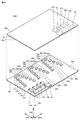
- FIG. 2A is an exploded perspective view of the power circuit device 100.
- the output side rectifying element 23a to the output side rectifying element 23d, the output terminal 22, and the output capacitor 24 are shown by dotted lines.
- FIG. 2B is a perspective view of the power circuit device 100.
- FIG. 2C is a perspective view of the power circuit device 100 in which the second substrate 50 is transparently displayed.
- the power circuit device 100 further includes a first substrate 40 and a second substrate 50.
- the first substrate 40 has a first surface 40a and a second surface 40b.
- the first surface 40a and the second surface 40b are the main surfaces of the first substrate 40.
- the second surface 40b is the opposite surface of the first surface 40a.
- the second substrate 50 has a first surface 50a and a second surface 50b.
- the first surface 50a and the second surface 50b are the main surfaces of the second substrate 50.
- the second surface 50b is the opposite surface of the first surface 50a.
- the first substrate 40 and the second substrate 50 are arranged at intervals in the first direction DR1 so that the first surface 40a and the second surface 50b face each other.
- the ground terminal 11 (not shown in FIGS. 2A to 2C), the input terminal 12, the input side switching element 13a to the input side switching element 13d, and the input capacitor 14 are arranged on the first surface 40a.
- the ground terminal 21 (not shown in FIGS. 2A to 2C), the output terminal 22, the output side rectifying element 23a to the output side rectifying element 23d, and the output capacitor 24 are arranged on the second surface 50b.
- the transformer 30 (transformer 31a to transformer 31e, transformer 32a to transformer 32e, transformer 33a to transformer 33e, transformer 34a to transformer 34e, transformer 35a to transformer 35e, and transformer 36a to transformer 36e) includes the first substrate 40 and the second substrate 50. (More specifically, between the first surface 40a and the second surface 50b).
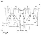
- FIG. 3A is a plan view of the power circuit device 100.
- the illustration of the second substrate 50 is omitted.
- the transformers 31a to 31e are arranged so as to form an inclined row (hereinafter, referred to as “first row L1”) with respect to the second direction DR2.
- the transformers 32a to 32e are arranged so as to form an inclined row (hereinafter referred to as "second row L2") with respect to the second direction DR2.
- the second direction DR2 is a direction orthogonal to the first direction DR1.
- the transformers 31a to 31e are arranged in this order from one side in the second direction DR2 (corresponding to the upper side in FIG. 3A) to the other side in the second direction DR2 (corresponding to the lower side in FIG. 3A). ing.
- the transformers 32a to 32e are arranged in this order from one side in the second direction DR2 toward the other side in the second direction DR2.
- the cooling air for cooling the transformer 30 is blown from the other side in the second direction DR2 to one side in the second direction DR2.
- the transformers 31a to 31e are arranged to face each other at a distance from the transformers 32a to 32e in the third direction DR3.
- the third direction DR3 is a direction orthogonal to the first direction DR1 and the second direction DR2.
- the distance between the transformer 31b and the transformer 32b in the third direction DR3 is wider than the distance between the transformer 31a and the transformer 32a in the third direction DR3.
- the distance between the transformer 31c and the transformer 32c in the third direction DR3 is wider than the distance between the transformer 31b and the transformer 32b in the third direction DR3.
- the distance between the transformer 31d and the transformer 32d in the third direction DR3 is wider than the distance between the transformer 31c and the transformer 32c in the third direction DR3.
- the distance between the transformer 31e and the transformer 32e in the third direction DR3 is wider than the distance between the transformer 31d and the transformer 32d in the third direction DR3.
- the distance between the first row L1 and the second row L2 in the third direction DR3 increases from one side in the second direction DR2 toward the other side in the second direction DR2. , Is spreading. That is, the distance between the first row L1 and the second row L2 in the third direction DR3 increases as it approaches the source of the cooling air.
- the transformers 33a to 33e and the transformers 35a to 35e are arranged so as to form the first row L1 respectively. Further, the transformers 34a to 34e and the transformers 36a to 36e are arranged so as to form the second row L2, respectively.
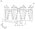
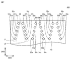
- FIG. 3B is a plan view of the power circuit device 100 according to the first modification.
- FIG. 3C is a plan view of the power circuit device 100 according to the second modification.
- the first row L1 and the second row L2 do not have to be linear in a plan view.
- the distance in the third direction DR3 between the transformers belonging to two adjacent first row L1s (belonging to the second row L2) is from one side to the second in the second direction DR2. It may become smaller (see FIG. 3B) or larger (see FIG. 3C) toward the other side in the direction DR2.
- FIG. 3D is a plan view of the power circuit device 100 according to the third modification.
- FIG. 3E is a plan view of the power circuit device 100 according to the fourth modification.
- the first row L1 and the second row L2 may be inclined in the same direction. In this case, the distance between the first row L1 and the second row L2 in the third direction DR3 does not widen from one side in the second direction DR2 toward the other side in the second direction DR2.
- wiring is formed on the first substrate 40 and the second substrate 50.
- the input terminal 12, the input side switching element 13a to the input side switching element 13d, the input capacitor 14, the ground terminal 21, the output terminal 22, the output side rectifying element 23a to the output side rectifying element 23d, the output capacitor 24 and the transformer 30. are connected as shown in FIG.
- the wiring of the primary circuit 10 is formed on the first substrate 40.
- the wiring of the secondary circuit 20 is formed on the second substrate 50.
- the first substrate 40 and the second substrate 50 may be formed with a solid pattern (a copper foil pattern that fills a large area) as a ground pattern at a portion where the above wiring is not formed.
- FIG. 4A is a side view of the power circuit device 100 when viewed along the third direction DR3.
- FIG. 4B is a side view of the power circuit device 100 when viewed along the second direction DR2.
- the transformers (transformers 32a to 32e) belonging to the second row L2 are the transformers (transformers) belonging to the first row L1 respectively. It is in a position overlapping with 31a to 31e).
- the transformers belonging to the first row L1 are positioned at different positions from each other, and the transformers belonging to the second row L2 are located.
- the second direction DR2 is a direction in which the transformers belonging to the first row L1 (second row L2) appear to be offset from each other
- the third direction DR3 is in the second row L2. This is the direction in which the transformer to which it belongs appears to overlap the transformer belonging to the first column L1.
- the power circuit device 100 is not limited to the DC / DC converter.
- the power circuit device 100 may be a circuit device including a transformer other than the DC / DC converter. Further, the above-mentioned number of rows and columns in the transformer 30 is an example.
- power circuit device 200 the power circuit device 200 according to the comparative example.
- the power circuit device 200 includes a primary side circuit 10, a secondary side circuit 20, a transformer 30, a first board 40, and a second board 50. In this respect, the configuration of the power circuit device 200 is common to the configuration of the power circuit device 100.
- FIG. 5 is a plan view of the power circuit device 200.
- the illustration of the second substrate 50 is omitted.
- the transformers 31a to 31e are arranged so as to form a row (hereinafter referred to as “third row L3”) along the second direction DR2.
- the transformers 32a to 32e, the transformers 33a to 33e, the transformers 34a to 34e, the transformers 35a to 35e, and the transformers 36a to 36e are arranged so as to form the third row L3, respectively.
- the configuration of the power circuit device 200 is different from the configuration of the power circuit device 100.
- the transformers 31a to 31e, the transformers 32a to 32e, the transformers 33a to 33e, the transformers 34a to 34e, the transformers 35a to 35e, and the transformers 36a to 36e are located along the second direction DR2. Since they are arranged so as to form three rows L3, the cooling air supplied to the transformer is on the other side of the second direction DR2 from the transformer (that is, at a position closer to the source of the cooling air than the transformer). (There is) It is easy to be disturbed by other transformers. As a result, the cooling effect of the cooling air becomes smaller as the transformer is on one side in the second direction DR2.
- the first row L1 and the second row L2 are inclined with respect to the second direction DR2, and between the first row L1 and the second row L2 in the third direction DR3. Since the interval extends from one side in the second direction DR2 toward the other side in the second direction DR2, the cooling air supplied to the transformer included in the first row L1 (second row L2) is in the first row. It is less likely to be disturbed by another transformer included in L1 and located on the other side of the second direction DR2 than the transformer.
- the distance between the first row L1 and the second row L2 in the third direction DR3 is from one side to the second in the second direction DR2. Although it does not extend toward the other side in the direction DR2, it is included in the first row L1 (second row L2) because the first row L1 (second row L2) is inclined with respect to the second direction DR2.
- the cooling air supplied to the transformer is contained in the first row L1 and is less likely to be obstructed by another transformer located on the other side of the second direction DR2 than the transformer.
- the power circuit device 100 it is possible to improve the uniformity of cooling for each transformer. Further, as a result of increasing the cooling uniformity for each transformer, the power circuit device 100 can be further miniaturized and operated at a higher temperature.
- the first board 40 and the second board 50 function as ducts. As a result, the cooling air can be supplied to the transformer 30 without being dissipated. Since the power circuit device 100 has a structure in which the transformer 30 is sandwiched between the first board 40 and the second board 50, the strength of the device can be increased.
- the wiring of the primary side circuit 10 and the wiring of the secondary side circuit 20 are mixed on one board. As a result, the substrate area increases. However, in the power circuit device 100, since the wiring of the primary side circuit 10 and the wiring of the secondary side circuit 20 are formed on the first board 40 and the second board 50, respectively, the area of each board is reduced. This makes it possible to reduce the size of the device. Further, in the power circuit device 100, as a result of the wiring of the primary side circuit 10 and the wiring of the secondary side circuit 20 being formed on the first board 40 and the second board 50, respectively, the wiring is simplified and the wiring impedance is increased. The resulting noise can be reduced.
- the solid pattern When a solid pattern (a copper foil pattern that fills a large area) is formed on the first substrate 40 and the second substrate 50 as a ground pattern, the solid pattern functions as an electromagnetic shield by sandwiching the power circuit.
- the amount of noise emitted to the outside and the amount of noise received from the outside can be reduced, and the noise resistance of the power circuit device 100 is improved. Further, in this case, the amount of the etching solution consumed in producing the first substrate 40 and the second substrate 50 can be reduced, so that the production cost can be reduced.
- power circuit device 300 the configuration of the power circuit device (hereinafter referred to as “power circuit device 300”) according to the second embodiment will be described.
- the points different from the configuration of the power circuit device 100 will be mainly described, and the duplicated description will not be repeated.
- the power circuit device 300 has a primary side circuit 10, a secondary side circuit 20, a transformer 30, a first board 40, and a second board 50.
- the transformers 31a to 31e, the transformers 33a to 33e, and the transformers 35a to 35e are arranged so as to form the first row L1.
- the transformers 32a to 32e, the transformers 34a to 34e, and the transformers 36a to 36e are arranged so as to form the second row L2, respectively.
- the configuration of the power circuit device 300 is common to the configuration of the power circuit device 100.
- FIG. 6 is a plan view of the power circuit device 300.
- the input terminal 12, the input side switching element 13a to the input side switching element 13d, the input capacitor 14, the ground terminal 21, the output terminal 22, the output side rectifying element 23a to the output side rectifying element 23d, the output capacitor 24, and The illustration of the second substrate 50 is omitted.
- the distance in the second direction DR2 between two adjacent transformers increases from the other side in the second direction DR2 toward one side in the second direction DR2. That is, the distance in the second direction DR2 between two adjacent transformers increases as the distance from the source of the cooling air increases.
- the configuration of the power circuit device 300 is different from the configuration of the power circuit device 100.
- the distance between the two adjacent transformers in the second direction DR2 increases as the distance from the source of the cooling air increases, so that the distance from the source of the cooling air increases, the more the cooling air passes through.
- the possible routes are widening. Therefore, in the power circuit device 300, it becomes easier to supply the cooling air to the transformer located at a position away from the source of the cooling air, so that the uniformity of cooling for each transformer can be further improved.
- power circuit device 400 the configuration of the power circuit device (hereinafter referred to as “power circuit device 400”) according to the third embodiment will be described.
- the points different from the configuration of the power circuit device 100 will be mainly described, and the duplicated description will not be repeated.
- the power circuit device 400 has a primary side circuit 10, a secondary side circuit 20, a transformer 30, a first board 40, and a second board 50.
- the transformers 31a to 31e, the transformers 33a to 33e, and the transformers 35a to 35e are arranged so as to form the first row L1.
- the transformers 32a to 32e, the transformers 34a to 34e, and the transformers 36a to 36e are arranged so as to form the second row L2, respectively.
- the configuration of the power circuit device 400 is common to the configuration of the power circuit device 100.
- FIG. 7 is a plan view of the power circuit device 400.
- the illustration of the second substrate 50 is omitted.
- each transformer included in the transformer 30 has a side surface 39.
- Each transformer included in the transformer 30 is arranged so that the side surface 39 is inclined with respect to the second direction DR2. That is, each of the transformers included in the transformer 30 is arranged so that the side surface 39 is inclined with respect to the direction of the cooling air.
- the configuration of the power circuit device 400 is different from the configuration of the power circuit device 100.
- the power circuit device 400 since the side surface 39 is inclined with respect to the direction of the cooling air, turbulence is unlikely to occur when the side surface 39 and the cooling air collide with each other. As a result, according to the power circuit device 400, it becomes easier to supply the cooling air to the transformers located at a position away from the source of the cooling air, so that the uniformity of cooling for each transformer can be further improved.
- power circuit device 500 the configuration of the power circuit device (hereinafter referred to as “power circuit device 500”) according to the fourth embodiment will be described.
- the points different from the configuration of the power circuit device 100 will be mainly described, and the duplicated description will not be repeated.
- the power circuit device 500 includes a primary side circuit 10, a secondary side circuit 20, a transformer 30, a first board 40, and a second board 50.
- the transformers 31a to 31e, the transformers 33a to 33e, and the transformers 35a to 35e are arranged so as to form the first row L1.
- the transformers 32a to 32e, the transformers 34a to 34e, and the transformers 36a to 36e are arranged so as to form the second row L2, respectively.
- the configuration of the power circuit device 500 is common to the configuration of the power circuit device 100.
- FIG. 8A is a perspective view of the power circuit device 500.
- FIG. 8B is a plan view of the power circuit device 500.
- FIG. 8C is a cross-sectional view of the power circuit device 500.
- FIG. 8C shows cross sections at positions corresponding to VIIIC-VIIIC in FIGS. 8A and 8B.
- the first substrate 40 is formed with a through hole 40c that penetrates the first substrate 40 in the thickness direction.
- the second substrate 50 is formed with a through hole 50c that penetrates the second substrate 50 in the thickness direction.
- the through hole 40c and the through hole 50c are formed at positions overlapping with each of the transformers included in the transformer 30 in a plan view.
- the power circuit device 500 further includes a resin member 60 and a resin member 70. In these respects, the configuration of the power circuit device 500 is different from the configuration of the power circuit device 100.
- the resin member 60 has a first portion 61, a second portion 62, and a third portion 63.
- the first portion 61 is on the first surface 40a and is in contact with each of the transformers included in the transformer 30. That is, each transformer included in the transformer 30 is adhered to the first substrate 40 by the resin member 60.
- the second portion 62 is on the second surface 40b.
- the third portion 63 is arranged in the through hole 40c and connects the first portion 61 and the second portion 62.
- the outer diameter of the resin member 60 in the first portion 61 and the second portion 62 is larger than the inner diameter of the through hole 40c.
- the resin member 70 has the same configuration as the resin member 60.
- the resin member 70 has a first portion 71, a second portion 72, and a third portion 73.
- the first portion 71 is on the second surface 50b and is in contact with each transformer included in the transformer 30 (each transformer included in the transformer 30 is adhered to the second substrate 50 by the resin member 70). Yes).
- the second portion 72 is on the first surface 50a.
- the third portion 73 is arranged in the through hole 50c and connects the first portion 71 and the second portion 72.
- the outer diameter of the resin member 70 in the first portion 71 and the second portion 72 is larger than the inner diameter of the through hole 50c.
- the resin member 60 and the resin member 70 are made of a resin material.
- the resin material is, for example, polypropylene (PP), acrylonitrile butadiene styrene (ABS), polyethylene terephthalate (PET), polycarbonate (PC), fluororesin, phenol resin, melamine resin, polyurethane, epoxy resin, silicone and the like.
- the resin member 60 and the resin member 70 may be formed of polybutylene terephthalate (PBT), polyphenylene sulfide (PPS), polyetheretherketone (PEEK), or the like containing a heat conductive filler.
- PBT polybutylene terephthalate
- PPS polyphenylene sulfide
- PEEK polyetheretherketone
- the heat generated in each of the transformers included in the transformer 30 is released to the surrounding space via the resin member 60 (resin member 70) and the first substrate 40 (second substrate 50). It will be. Therefore, according to the power circuit device 500, the heat dissipation performance is improved.
- each transformer included in the transformer 30 is adhered to the first substrate 40 (second substrate 50) by the resin member 60 (resin member 70). Therefore, according to the power circuit device 500, the impact resistance can be improved.
Landscapes
- Engineering & Computer Science (AREA)
- Power Engineering (AREA)
- Dc-Dc Converters (AREA)
- Transformer Cooling (AREA)
Priority Applications (1)
| Application Number | Priority Date | Filing Date | Title |
|---|---|---|---|
| JP2022524408A JP7305044B2 (ja) | 2020-05-21 | 2021-05-12 | 電力回路装置 |
Applications Claiming Priority (2)
| Application Number | Priority Date | Filing Date | Title |
|---|---|---|---|
| JP2020-088546 | 2020-05-21 | ||
| JP2020088546 | 2020-05-21 |
Publications (1)
| Publication Number | Publication Date |
|---|---|
| WO2021235288A1 true WO2021235288A1 (ja) | 2021-11-25 |
Family
ID=78707865
Family Applications (1)
| Application Number | Title | Priority Date | Filing Date |
|---|---|---|---|
| PCT/JP2021/018016 Ceased WO2021235288A1 (ja) | 2020-05-21 | 2021-05-12 | 電力回路装置 |
Country Status (2)
| Country | Link |
|---|---|
| JP (1) | JP7305044B2 (https=) |
| WO (1) | WO2021235288A1 (https=) |
Citations (9)
| Publication number | Priority date | Publication date | Assignee | Title |
|---|---|---|---|---|
| JPH07106732A (ja) * | 1993-10-05 | 1995-04-21 | Fujitsu Ltd | コンデンサの実装構造 |
| WO2002049106A1 (fr) * | 2000-12-11 | 2002-06-20 | Fujitsu Limited | Module électronique |
| US20030183909A1 (en) * | 2002-03-27 | 2003-10-02 | Chia-Pin Chiu | Methods and apparatus for disposing a thermal interface material between a heat source and a heat dissipation device |
| JP2008125249A (ja) * | 2006-11-13 | 2008-05-29 | Densei Lambda Kk | 電源装置 |
| JP2008187136A (ja) * | 2007-01-31 | 2008-08-14 | Densei Lambda Kk | 放熱構造 |
| WO2012158523A2 (en) * | 2011-05-13 | 2012-11-22 | Google Inc. | Air-cooled data center rows |
| JP2013051258A (ja) * | 2011-08-30 | 2013-03-14 | Shindengen Electric Mfg Co Ltd | トランス装置 |
| US8498124B1 (en) * | 2009-12-10 | 2013-07-30 | Universal Lighting Technologies, Inc. | Magnetic circuit board stacking component |
| WO2018202439A1 (de) * | 2017-05-02 | 2018-11-08 | Siemens Aktiengesellschaft | Elektronische baugruppe mit einem zwischen zwei substraten eingebauten bauelement und verfahren zu dessen herstellung |
-
2021
- 2021-05-12 WO PCT/JP2021/018016 patent/WO2021235288A1/ja not_active Ceased
- 2021-05-12 JP JP2022524408A patent/JP7305044B2/ja active Active
Patent Citations (9)
| Publication number | Priority date | Publication date | Assignee | Title |
|---|---|---|---|---|
| JPH07106732A (ja) * | 1993-10-05 | 1995-04-21 | Fujitsu Ltd | コンデンサの実装構造 |
| WO2002049106A1 (fr) * | 2000-12-11 | 2002-06-20 | Fujitsu Limited | Module électronique |
| US20030183909A1 (en) * | 2002-03-27 | 2003-10-02 | Chia-Pin Chiu | Methods and apparatus for disposing a thermal interface material between a heat source and a heat dissipation device |
| JP2008125249A (ja) * | 2006-11-13 | 2008-05-29 | Densei Lambda Kk | 電源装置 |
| JP2008187136A (ja) * | 2007-01-31 | 2008-08-14 | Densei Lambda Kk | 放熱構造 |
| US8498124B1 (en) * | 2009-12-10 | 2013-07-30 | Universal Lighting Technologies, Inc. | Magnetic circuit board stacking component |
| WO2012158523A2 (en) * | 2011-05-13 | 2012-11-22 | Google Inc. | Air-cooled data center rows |
| JP2013051258A (ja) * | 2011-08-30 | 2013-03-14 | Shindengen Electric Mfg Co Ltd | トランス装置 |
| WO2018202439A1 (de) * | 2017-05-02 | 2018-11-08 | Siemens Aktiengesellschaft | Elektronische baugruppe mit einem zwischen zwei substraten eingebauten bauelement und verfahren zu dessen herstellung |
Also Published As
| Publication number | Publication date |
|---|---|
| JP7305044B2 (ja) | 2023-07-07 |
| JPWO2021235288A1 (https=) | 2021-11-25 |
Similar Documents
| Publication | Publication Date | Title |
|---|---|---|
| US5488255A (en) | Cooling device for semiconductor packages, having flexible film heat expulsion means | |
| JP7237475B2 (ja) | パワーモジュール及びスイッチング電源 | |
| EP3582598A1 (en) | Low profile, highly configurable, current sharing paralleled wide band gap power device power module | |
| US10186481B2 (en) | Semiconductor device including a passive component formed in a redistribution layer | |
| US20200303112A1 (en) | MAGNETIC DEVICE and STACKED ELECTRONIC STRUCTURE | |
| JP2022163097A (ja) | トランス及び電力変換装置 | |
| WO2021261508A1 (ja) | 半導体装置 | |
| JP4652434B2 (ja) | 可変インダクタ及びこれを回路構成に組み入れた電子回路装置 | |
| JP7305044B2 (ja) | 電力回路装置 | |
| WO2020189291A1 (ja) | コイル装置および電力変換装置 | |
| JP6577374B2 (ja) | 半導体装置 | |
| JPWO2018211643A1 (ja) | 増幅器 | |
| US20210272749A1 (en) | Electronic device | |
| JP7705986B2 (ja) | 半導体装置 | |
| JP6827566B2 (ja) | コイル装置および電力変換装置 | |
| KR102569184B1 (ko) | 반도체칩을 구비한 반도체 부품과 쿨링장치가 결합된 쿨링시스템 | |
| JP2024129909A (ja) | トランス及び電力変換装置 | |
| JP7595757B2 (ja) | 電力変換装置 | |
| CN113632216B (zh) | 功率基板及具备该功率基板的高电压模块 | |
| US10186607B2 (en) | Power semiconductor device including a semiconductor switching element | |
| US10368431B2 (en) | Cooling assemblies for electronic devices | |
| EP4184570A2 (en) | Power electronic module with reduced mutual inductance between power and control loops | |
| JP7342509B2 (ja) | 半導体装置 | |
| US20250314678A1 (en) | Planar current sensor for power conversion applications | |
| WO2025202413A1 (de) | Schallaktuator |
Legal Events
| Date | Code | Title | Description |
|---|---|---|---|
| 121 | Ep: the epo has been informed by wipo that ep was designated in this application |
Ref document number: 21808896 Country of ref document: EP Kind code of ref document: A1 |
|
| ENP | Entry into the national phase |
Ref document number: 2022524408 Country of ref document: JP Kind code of ref document: A |
|
| NENP | Non-entry into the national phase |
Ref country code: DE |
|
| 122 | Ep: pct application non-entry in european phase |
Ref document number: 21808896 Country of ref document: EP Kind code of ref document: A1 |