WO2021229848A1 - 光学系装置および光学素子製造方法 - Google Patents
光学系装置および光学素子製造方法 Download PDFInfo
- Publication number
- WO2021229848A1 WO2021229848A1 PCT/JP2020/047275 JP2020047275W WO2021229848A1 WO 2021229848 A1 WO2021229848 A1 WO 2021229848A1 JP 2020047275 W JP2020047275 W JP 2020047275W WO 2021229848 A1 WO2021229848 A1 WO 2021229848A1
- Authority
- WO
- WIPO (PCT)
- Prior art keywords
- light
- lens
- irradiation unit
- optical element
- optical system
- Prior art date
- Legal status (The legal status is an assumption and is not a legal conclusion. Google has not performed a legal analysis and makes no representation as to the accuracy of the status listed.)
- Ceased
Links
Images






















Classifications
-
- G—PHYSICS
- G02—OPTICS
- G02B—OPTICAL ELEMENTS, SYSTEMS OR APPARATUS
- G02B3/00—Simple or compound lenses
- G02B3/0006—Arrays
- G02B3/0037—Arrays characterized by the distribution or form of lenses
- G02B3/0056—Arrays characterized by the distribution or form of lenses arranged along two different directions in a plane, e.g. honeycomb arrangement of lenses
-
- G—PHYSICS
- G01—MEASURING; TESTING
- G01S—RADIO DIRECTION-FINDING; RADIO NAVIGATION; DETERMINING DISTANCE OR VELOCITY BY USE OF RADIO WAVES; LOCATING OR PRESENCE-DETECTING BY USE OF THE REFLECTION OR RERADIATION OF RADIO WAVES; ANALOGOUS ARRANGEMENTS USING OTHER WAVES
- G01S7/00—Details of systems according to groups G01S13/00, G01S15/00, G01S17/00
- G01S7/48—Details of systems according to groups G01S13/00, G01S15/00, G01S17/00 of systems according to group G01S17/00
- G01S7/481—Constructional features, e.g. arrangements of optical elements
-
- G—PHYSICS
- G02—OPTICS
- G02B—OPTICAL ELEMENTS, SYSTEMS OR APPARATUS
- G02B3/00—Simple or compound lenses
- G02B3/0006—Arrays
- G02B3/0037—Arrays characterized by the distribution or form of lenses
-
- G—PHYSICS
- G02—OPTICS
- G02B—OPTICAL ELEMENTS, SYSTEMS OR APPARATUS
- G02B3/00—Simple or compound lenses
- G02B3/02—Simple or compound lenses with non-spherical faces
- G02B3/04—Simple or compound lenses with non-spherical faces with continuous faces that are rotationally symmetrical but deviate from a true sphere, e.g. so called "aspheric" lenses
-
- G—PHYSICS
- G02—OPTICS
- G02B—OPTICAL ELEMENTS, SYSTEMS OR APPARATUS
- G02B5/00—Optical elements other than lenses
- G02B5/02—Diffusing elements; Afocal elements
- G02B5/0273—Diffusing elements; Afocal elements characterized by the use
- G02B5/0284—Diffusing elements; Afocal elements characterized by the use used in reflection
-
- G—PHYSICS
- G02—OPTICS
- G02B—OPTICAL ELEMENTS, SYSTEMS OR APPARATUS
- G02B5/00—Optical elements other than lenses
- G02B5/02—Diffusing elements; Afocal elements
- G02B5/0273—Diffusing elements; Afocal elements characterized by the use
- G02B5/0294—Diffusing elements; Afocal elements characterized by the use adapted to provide an additional optical effect, e.g. anti-reflection or filter
-
- G—PHYSICS
- G02—OPTICS
- G02B—OPTICAL ELEMENTS, SYSTEMS OR APPARATUS
- G02B5/00—Optical elements other than lenses
- G02B5/08—Mirrors
- G02B5/0808—Mirrors having a single reflecting layer
-
- G—PHYSICS
- G02—OPTICS
- G02B—OPTICAL ELEMENTS, SYSTEMS OR APPARATUS
- G02B5/00—Optical elements other than lenses
- G02B5/20—Filters
- G02B5/28—Interference filters
-
- H—ELECTRICITY
- H01—ELECTRIC ELEMENTS
- H01S—DEVICES USING THE PROCESS OF LIGHT AMPLIFICATION BY STIMULATED EMISSION OF RADIATION [LASER] TO AMPLIFY OR GENERATE LIGHT; DEVICES USING STIMULATED EMISSION OF ELECTROMAGNETIC RADIATION IN WAVE RANGES OTHER THAN OPTICAL
- H01S5/00—Semiconductor lasers
- H01S5/10—Construction or shape of the optical resonator, e.g. extended or external cavity, coupled cavities, bent-guide, varying width, thickness or composition of the active region
- H01S5/18—Surface-emitting [SE] lasers, e.g. having both horizontal and vertical cavities
- H01S5/183—Surface-emitting [SE] lasers, e.g. having both horizontal and vertical cavities having only vertical cavities, e.g. vertical cavity surface-emitting lasers [VCSEL]
-
- H—ELECTRICITY
- H01—ELECTRIC ELEMENTS
- H01S—DEVICES USING THE PROCESS OF LIGHT AMPLIFICATION BY STIMULATED EMISSION OF RADIATION [LASER] TO AMPLIFY OR GENERATE LIGHT; DEVICES USING STIMULATED EMISSION OF ELECTROMAGNETIC RADIATION IN WAVE RANGES OTHER THAN OPTICAL
- H01S5/00—Semiconductor lasers
- H01S5/005—Optical components external to the laser cavity, specially adapted therefor, e.g. for homogenisation or merging of the beams or for manipulating laser pulses, e.g. pulse shaping
-
- H—ELECTRICITY
- H01—ELECTRIC ELEMENTS
- H01S—DEVICES USING THE PROCESS OF LIGHT AMPLIFICATION BY STIMULATED EMISSION OF RADIATION [LASER] TO AMPLIFY OR GENERATE LIGHT; DEVICES USING STIMULATED EMISSION OF ELECTROMAGNETIC RADIATION IN WAVE RANGES OTHER THAN OPTICAL
- H01S5/00—Semiconductor lasers
- H01S5/40—Arrangement of two or more semiconductor lasers, not provided for in groups H01S5/02 - H01S5/30
- H01S5/42—Arrays of surface emitting lasers
- H01S5/423—Arrays of surface emitting lasers having a vertical cavity
Definitions
- the present invention relates to an optical system device and an optical element manufacturing method.
- Three-dimensional measurement sensors using the time of flight (TOF) method are about to be adopted in mobile devices, cars, robots, etc. This measures the distance of an object from the time it takes for the light emitted from the light source to be reflected and returned to the object. If the light from the light source is uniformly applied to a predetermined area of the object, the distance at each point of irradiation can be measured and the three-dimensional structure of the object can be detected.
- TOF time of flight
- the sensor system consists of a light irradiation unit that irradiates the object with light, a camera unit that detects the light reflected from each point of the object, and a calculation unit that calculates the distance of the object from the signal received by the camera.
- the unique part of the above system is the light irradiation unit consisting of the laser and the optical filter.
- a diffusion filter that shapes a beam by transmitting laser light through a microlens array and uniformly irradiates an object in a controlled region is a characteristic component of the above system.
- the conventional diffusion filter has a problem that the light intensity becomes uneven due to the influence of diffraction because the microlens array has a periodic structure. Therefore, in order to suppress this unevenness, some measures have been taken such as randomly arranging each lens (for example, Patent Document 1).
- TOF has a need for long-distance measurement, and the intensity of irradiation light needs to be strong enough for long-distance measurement.
- the randomly arranged microlens array is not suitable for long-distance measurement because the intensity is low due to the high uniformity of the irradiation light.
- a diffractive optical element which is composed of a concave-convex pattern of a dielectric and changes the phase difference of light depending on the position of a transmission surface
- DOE diffractive optical element
- VCSEL vertically resonant surface emitting laser
- the light emitted from the VCSEL is first converted into parallel light by the collimating lens.
- the collimated light passes through the uneven pattern to change the phase difference, and the diffraction of the light gives a predetermined orientation distribution.
- the surface of the object to be irradiated is irradiated with light with a predetermined intensity distribution.
- the light emitted by the VCSEL has a spread angle of about 20 degrees, and when used for a dot projector, a collimating lens is required as described above.
- a collimated lens in order to generate collimated light, it is necessary to arrange a light source at the focal position of the lens. In order to obtain high quality collimated light, there is a problem that the focal length is long and the device size becomes large.
- an object of the present invention is to provide an optical system device that does not require a collimating lens and has high light efficiency that can be used, and a method for manufacturing an optical element used in the device.
- the optical system apparatus of the present invention includes an optical element in which lenses transmitting light having a wavelength ⁇ are periodically arranged, and a light source that irradiates a plurality of lenses having a wavelength ⁇ light.
- n is a natural number of 1 or more
- the distance L 1 between the irradiation unit and the optical element is the following equation 1 with respect to the pitch P k of. It is characterized by satisfying.
- the lens should be an aspherical lens having an overlap rate of 10% or less in the normal direction of the surface.
- the aperture mask may have an opening and be equipped with an aperture mask for shielding a part of light.
- the aperture mask may have an aperture at least in a portion including the optical axis of the lens. Further, the aperture mask may be arranged in the optical path of the noise light of the lens. The aperture mask may be arranged at the boundary portion of the lens. Further, an aperture mask that shields the light emitted to the boundary portion of the lens may be provided.
- the aperture mask may be integrally formed with the optical element.
- the optical element may have a light diffusing portion formed at the boundary portion of the lens to refract the transmitted light to the outside of the irradiation angle of the lens.
- the shape of the lens can be non-rotational symmetry.
- a mirror that reflects the light of the irradiation unit may be provided.
- optical system device of the present invention may include a plurality of the irradiation units.
- the irradiation unit includes a first irradiation unit in which a plurality of light sources irradiating light having a wavelength ⁇ are regularly arranged, and a plurality of light sources irradiating light having a wavelength ⁇ vertically and vertically with the light source of the first irradiation unit. It may be composed of a second irradiation part which is arranged side by side by half a cycle and regularly arranged.
- the irradiation unit includes a first irradiation unit, a second irradiation unit, and a third irradiation unit in which a plurality of light sources irradiating light having a wavelength ⁇ are regularly arranged, and the lens of the optical element has a pitch Pk .
- the light sources of the first irradiation unit, the second irradiation unit, and the third irradiation unit may be arranged so as to be shifted by Pk / 3 with respect to the direction to be taken.
- each of the irradiation units may be one that emits light in order with a time lag.
- planar shape of the lens is a square or a rectangle whose side length is R, and the arrangement of the lenses is a row of lenses connected in the direction of the sides, where i is a natural number of 1 or more. They may be arranged so as to be staggered by R / i.
- the irradiation unit is composed of a VCSEL having a plurality of light emission modes, and it is preferable that the ratio of the mode having the maximum intensity at the center of the optical axis is 40% or more in the light emission mode.
- the irradiation unit regularly arranges a plurality of light sources at m times or 1 / m times of the period with respect to any periodic direction of the lens of the optical element. It was done.
- the optical system device of the present invention is arranged between the diffuser that diffuses the light of the irradiation unit into a predetermined shape and the light source and the diffuser, and transmits a part of the light of the irradiation unit to partially transmit the light.
- a half mirror that reflects the light and a mirror that reflects the light reflected by the half mirror to the optical element may be further provided.
- the optical system device of the present invention includes a diffuser irradiation unit in which a plurality of light sources irradiating light having a wavelength ⁇ are arranged in the same manner as the irradiation unit, and the distance L 2 between the diffuser irradiation unit and the optical element is provided.
- the following formula 2 It may satisfy.
- the optical system device of the present invention includes a diffuser irradiation unit in which a plurality of light sources irradiating light having a wavelength ⁇ are arranged, and when m is a natural number of 1 or more, the diffuser irradiation unit is the optical element.
- a plurality of light sources may be arranged so as not to be m times or 1 / m times the period of the lens with respect to the period direction of the lens.
- the optical system device of the present invention includes the diffuser irradiation unit having the same regular arrangement as the light source of the irradiation unit, and the rotation angles of the irradiation unit and the diffuser irradiation unit may be different.
- the optical element manufacturing method of the present invention is an optical element manufacturing method for forming an optical element in which lenses transmitting light having a wavelength ⁇ are periodically arranged, and is one of the light transmitted through the lens on a substrate. It is characterized by having an aperture mask forming step of forming an aperture mask for shielding a portion and a lens forming step of forming the lens on a substrate on which the aperture mask is formed.
- the lens in the lens forming step, the lens may be formed so that the aperture mask is arranged in the optical path of the noise light of the lens.
- the lens in the lens forming step, the lens may be formed so that the boundary of the lens is arranged on the shielding portion of the aperture mask.
- the optical element manufacturing method of the present invention is an optical element manufacturing method for forming an optical element in which lenses transmitting light having a wavelength ⁇ are periodically arranged, and the light is transmitted on the lens. It is characterized by having an aperture mask forming step of applying a light-shielding material to prevent the light-shielding material and removing the light-shielding material so that a part of the light-shielding material remains at a position corresponding to the boundary of the lens.
- the optical system device of the present invention does not require a collimating lens and can irradiate light with high efficiency of available light.
- the optical system apparatus of the present invention is mainly composed of an irradiation unit 1 that irradiates light having a wavelength ⁇ and an optical element 2 having a periodic lens 21.
- the irradiation unit 1 may be any one as long as it irradiates light having a wavelength ⁇ . Further, the irradiation unit 1 may be a single light source or a plurality of light sources. Further, a plurality of light sources may be obtained by passing the light of a single light source through an aperture in which a plurality of pores are formed. When the irradiation unit is composed of a plurality of light sources, it is preferable that the light sources are formed on the same plane. As a specific example of the irradiation unit 1, for example, a VCSEL (Vertical Cavity Surface Emitting LASER), which can be expected to have a high output with a small amount of electric power, can be mentioned. The VCSEL has a plurality of light sources 10 capable of irradiating light in a direction perpendicular to the light emitting surface.
- VCSEL Very Cavity Surface Emitting LASER
- the light of the VCSEL includes a plurality of light emission modes such as a single mode and a multi-mode.
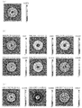
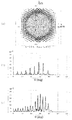
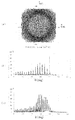
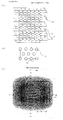
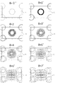
- An example of a specific light emission mode is shown in FIG. Of the emission modes shown in FIG. 2, (2) and (3), (4) and (6), (7) and (9), and (8) and (10), which are rotationally symmetric with each other, always exist at the same ratio. Therefore, when these similar modes are combined, they can be aggregated into six types, A, B, C, D, E, and F, as shown in FIG.
- FIG. 4 (c) is a composite of the six modes, in which only mode A, mode D, and mode F are multiplied by five of the other modes.
- the light source of the VCSEL has a large proportion of the light emission modes having the maximum intensity at the center of the optical axis among the light emission modes. It is preferable in that the light intensity can be increased and the contrast can be increased. Therefore, the ratio of the light emitting mode of the light source having the maximum intensity at the center of the optical axis is preferably 40% or more, preferably 45% or more, and more preferably 60% or more.
- the light emission mode may be adjusted by a conventionally known method such as controlling the current injection path of the light emitting layer of the VCSEL.
- the optical element 2 is a periodic array of lenses 21 that transmit light having a wavelength of ⁇ .
- the shape of the lens 21 can be freely designed according to the pattern of how the dots to be irradiated are spread (hereinafter referred to as a dot pattern). For example, when the dot pattern is desired to be circular, the shape of the lens 21 may be rotationally symmetric like a spherical lens. Further, when it is desired to make the dot pattern non-circular, the shape of the lens 21 may be appropriately adjusted by making it non-rotational symmetric like an aspherical lens.
- Specific lens shapes include, for example, a saddle-shaped lens that looks like a convex lens or a concave lens depending on the cross section, in addition to a convex lens and a concave lens.
- the periodic arrangement includes a square or rectangular lens 21 arranged in a square arrangement in a plan view as shown in FIG. 5 (a) and a hexagonal lens 21 in a plan view as shown in FIG. 5 (b). Applicable to those that make a hexagonal arrangement.
- the distance L 0 is expressed by the following formula A.
- the light is greatly strengthened.
- the distance between the irradiation unit 1 and the optical element 2 means the distance from the light emitting surface of the light source of the irradiation unit to the surface of the optical element on the side close to the light source of the lens 21.
- the distance L between the irradiation unit 1 and the optical element 2 greatly intensifies the light even when the distance L is n times the distance L 0 (n is a natural number of 1 or more) as shown in the following formula B. Furthermore, it was found that when n is an even number, the light is further enhanced.
- the error with respect to the distance L between the irradiation unit 1 and the optical element 2 is preferably within 10%, preferably within 5%, and more preferably within 3% of L 0.
- Specifically expressing that the error with respect to the distance L is within 10% of L 0 can be expressed as the following equation C.
- the irradiation unit 1 and the optics are used for any one or more pitch P k.
- the distance L 1 from the element 2 is the following equation 1 You just have to meet.
- the distance L between the irradiation unit 1 and the optical element 2 is preferable to adjust the distance L between the irradiation unit 1 and the optical element 2 so as to satisfy the equation 1 for any two or more pitches P k.
- the equation 1 is also applied to the second smallest pitch P 2. Better to meet.
- the pitch P is too smaller than the wavelength ⁇ of the light of the light source 10, diffraction is unlikely to occur. Therefore, as long as the lens 21 sufficient to generate diffraction is included in the light distribution angle of the light source 10, the pitch is pitched.
- P should be sufficiently larger than the wavelength ⁇ of the light of the light source 10, for example, 5 times or more, preferably 10 times or more.
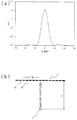
- the irradiation unit 1 is a single light source that irradiates light having a wavelength of 940 nm and having a Gaussian light distribution as shown in FIG. 16 (a).
- the optical element 2 is a lens 21 having a height of 7 ⁇ m arranged periodically at a pitch of 10 ⁇ m.
- the lens surface has a non-arc shape.
- the material was assumed to be PDMS with a refractive index of 1.53.
- n in the formula A is 1, 2, 4, 6, 8.
- FIG. 17 shows the results of a simulation using the optical simulation software BeamPROP (manufactured by Synopsys).
- the horizontal axis is the light distribution angle
- the vertical axis is the light intensity in the far field at each light distribution angle when the power of the light source is 1.
- the light intensity of each peak Turned out to be big.
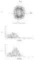
- the irradiation unit 1 is a plurality of light sources in which the light sources 10 for irradiating light having a wavelength of 940 nm are arranged in a square array as shown in FIG. 18 (a). Further, the light emitted by the light source had a butt wing light distribution as shown in FIG. 18 (b) and had a light intensity as shown in FIG. 18 (c) in the distant field.
- the optical element 2 is a square array of lenses 21 having a pitch of 20 ⁇ m. Further, as shown in FIG. 19B, the shape of each lens 21 is a square having a side view of 20 ⁇ m and a height of 9.86 ⁇ m.
- the lens surface is an aspherical surface with non-rotational symmetry having different curvatures in the x-axis direction and the y-axis direction.
- the material was assumed to be PDMS with a refractive index of 1.53.
- 20 to 22 show the results of simulation using the optical simulation software BeamPROP (manufactured by Synopsys).
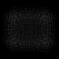
- 20 to 22 (a) are views showing a dot pattern 50 cm ahead of the optical element 2. The size of the dots represents the size of the light intensity. Further, (b) of FIGS.
- FIGS. 20 to 22 shows the light intensity in the far field of the light on the x-axis of FIGS. 20 to 22 (a), and FIGS. 20 to 22 (c) show the light intensity of FIGS. 20 to 22.
- (A) shows the light intensity in the far field of light on the y-axis.
- the horizontal axis is the light distribution angle
- the vertical axis is the light intensity in the far field at each light distribution angle when the power of the light source is 1.
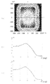
- FIG. 23 shows the results of a simulation using the optical simulation software LightTools (manufactured by Synopsys).
- FIG. 23A is a diagram showing an irradiation pattern 50 cm ahead of the diffuser.
- FIG. 23 (b) shows the light intensity in the far field of the light on the x-axis of FIG. 23 (a)
- FIG. 23 (c) shows the light intensity of the light in the far field on the y-axis of FIG. 23 (a). Is shown.
- the dot pattern has clear peaks and the light intensity of each peak is also high.
- the light intensity of each peak is very high as compared with the one using the diffuser.
- L having this pitch satisfying the formula A is 425.5 ⁇ m, it can be seen that the peaks are more clearly aligned and the light intensity is higher in the result of FIG. 21 than in the result of FIG.
- the irradiation unit 1 has a plurality of light sources in which the light sources irradiating light having a wavelength of 940 nm are arranged in a hexagonal arrangement as shown in FIG. 24 (a). Further, the light emitted by the light source had a butt wing light distribution as shown in FIG. 24 (b) and had a light intensity as shown in FIG. 24 (c) in the distant field.
- the optical element 2 is a hexagonal array of lenses 21 having a pitch of 22.5 ⁇ m. Further, as shown in FIG. 25B, the shape of each lens 21 is a regular hexagon in a plan view and a height of 12.9 ⁇ m.
- the lens surface is an aspherical surface with non-rotational symmetry having different curvatures in the x-axis direction and the y-axis direction.
- the material was assumed to be PDMS with a refractive index of 1.53.
- Figures 26 to 28 show the results of simulation using the optical simulation software BeamPROP (manufactured by Synopsys). Note that FIGS. 26 to 28 (a) are views showing a dot pattern 50 cm ahead of the optical element 2. The size of the dots represents the size of the light intensity.
- FIGS. 26 to 28 shows the light intensity in the far field of the light on the x-axis of (a) of FIGS. 26 to 28, and (c) of FIGS. 26 to 28 (a) of FIGS. 26 to 28.
- the horizontal axis is the light distribution angle
- the vertical axis is the light intensity in the far field at each light distribution angle when the power of the light source is 1.
- FIG. 29 shows a simulation result when a diffuser capable of forming an irradiation pattern having substantially the same shape as the above dot pattern is used.
- FIG. 29A is a diagram showing an irradiation pattern 50 cm ahead of the diffuser.
- FIG. 29 (b) shows the light intensity in the far field of the light on the x-axis of FIG. 29 (a)
- FIG. 29 (c) shows the light intensity of the light in the far field on the y-axis of FIG. 29 (a). Is shown.
- the dot pattern has clear peaks and the light intensity of each peak is also high.
- the light intensity of each peak is very high as compared with the one using the diffuser.
- the lens shape of the optical element 2 was further examined. Then, it was found that when light transmitted through different positions on the surface of the lens 21 is emitted in the same direction, interference occurs, which causes a decrease in dot contrast. Therefore, it is preferable that the optical element is designed so that the overlap rate in the emission direction of the transmitted light from the lens 21 is low.
- the lens 21 may be shaped so that the overlap rate in the normal direction of the surface is low.
- the lens 21 has an inflection point or a singular point in which the lens 21 changes from concave to convex or convex to concave in a line in a cross section of the surface of the lens 21, the concave and convex portions before and after the lens 21 have an inflection point and a convex portion. Overlapping surfaces in the normal direction occur.
- FIG. 30 shows an example of a lens having an inflection point
- FIG. 31 shows an example of a lens having no inflection point
- FIGS. 30 (b) and 31 (b) show the light intensity in the far field of the dot pattern when the optical element in which the lens is periodically arranged is used.
- the irradiation unit 1 is a single light source that irradiates light having a wavelength of 940 nm and having a Gaussian light distribution as shown in FIG. 16 (a).
- the optical element 2 is a lens 21 having a height of 10 ⁇ m arranged periodically at a pitch of 10 ⁇ m.
- the material was assumed to be PDMS with a refractive index of 1.53.
- As the distance L, 106.4 ⁇ m (n 2) when n in the formula A was 2. was used.
- 31 (b) and 32 (b) show the results of a simulation using the optical simulation software BeamPROP (manufactured by Synopsys).
- the horizontal axis is the light distribution angle
- the vertical axis is the light intensity in the far field at each light distribution angle when the power of the light source is 1.
- the shape of the lens changes from concave to convex or from convex to concave at this portion. In this case, there is a region where the light transmitted through the convex portion and the light transmitted through the concave portion travel in the same direction. Therefore, as shown in FIG. 30B, noise light is generated between the dots due to the interference, and the contrast is increased. It becomes a factor to lower.
- the shape of the lens is composed of only a convex portion.
- the transmitted light does not overlap, a clean dot pattern without noise light can be formed as shown in FIG. 31 (b). Therefore, it is preferable that the line in the cross section of the surface of the lens 21 has no inflection point or singular point, and even if such a point is present, it is preferable that either the concave portion or the convex portion has a sufficiently large shape. good.
- the overlap rate in the normal direction of the surface of the lens 21 can be measured as follows.
- the lens 21 is divided into n pieces as a square fine region 210 in a plan view (xy plane). Then, the numbers 1 to n that do not overlap are assigned to each of the fine regions 210.
- the size of one side of the fine region 210 is at least one-fourth ( ⁇ / 4) or less of the wavelength of the light of the irradiation unit.
- i-th among the divided micro areas 210 (i 1,2, ⁇ , n) the center point P i of the fine region, the circle inscribed C Let i be.
- FIG. 32 (b) as shown in the point P i and a line perpendicular to the x-y plane passing through the (z-axis line parallel to) the normal vector at the intersection of the lens surface N pi, circle C i
- N ci be the normal vector group at the intersection of the line perpendicular to the xy plane (the line parallel to the z-axis) passing through the lens surface.
- the minimum value of the angle formed by N pi and N ci is ⁇ ⁇ i .
- N qi be a normal vector group at the intersection of a line perpendicular to the xy plane (a line parallel to the z axis) passing through the point group Q i and the lens surface. .. (5) a state flag of the i-th fine regions and F i of the divided micro areas 210, the initial value of F i and 0. (6)
- the normal overlap rate can be obtained by (m / n) ⁇ 100 (%). The normal overlap rate converges when n is set to infinity (n ⁇ ⁇ ).
- the irradiation unit 1 is a plurality of light sources in which the light sources 10 for irradiating light having a wavelength of 940 nm are arranged in a square array as shown in FIG. 18 (a). Further, the light emitted by the light source had a butt wing light distribution as shown in FIG. 18 (b) and had a light intensity as shown in FIG.
- the material was assumed to be PDMS with a refractive index of 1.53.
- Optical simulation software BeamPROP manufactured by Synopsys was used for the simulation.
- FIG. 33 (a) The lens shown in FIG. 33 (a) will be described as a model 1.
- the shape of the lens is as follows.
- the white area in FIG. 33 (b) was a region where the normals did not overlap, and the normal overlap rate was 0%.
- FIGS. 33 (c) and 33 (d) show the light intensity in the distant field. It can be seen that there is almost no noise light and the peak light intensity is strong as a whole.
- FIG. 34 (a) The lens shown in FIG. 34 (a) will be described as a model 2.
- the shape of the lens is as follows.
- the black area in FIG. 34 (b) is the area where the normals overlap, and the normal overlap rate was 5.3%.
- FIGS. 34 (c) and 34 (d) show the light intensity in the distant field. Although there is little noise light, it can be seen that the peak light intensity is slightly lower than that of Model 1.
- FIG. 35 (a) The lens shown in FIG. 35 (a) will be described as a model 3.
- the shape of the lens is as follows.
- the black area in FIG. 35 (b) is the area where the normals overlap, and the normal overlap rate was 12.8%.
- FIGS. 35 (c) and 35 (d) show the light intensity in the distant field. It can be seen that the normal overlap rate exceeds 10% as compared with model 1, and the light intensity of the peak is further lowered as compared with model 1 and model 2.
- FIG. 36 (a) The lens shown in FIG. 36 (a) will be described as a model 4.
- the shape of the lens is as follows.
- the black area in FIG. 36 (b) is the area where the normals overlap, and the normal overlap rate was 49.8%.
- FIGS. 36 (c) and 36 (d) show the light intensity in the distant field. It can be seen that the normal overlap rate is higher than that of Model 3 and the light intensity is weak as a whole.
- FIG. 37 (a) The lens shown in FIG. 37 (a) will be described as a model 5.
- the shape of the lens is as follows.
- the black area in FIG. 37 (b) is the area where the normals overlap, and the normal overlap rate was 62.2%.
- FIGS. 37 (c) and 37 (d) show the light intensity in the distant field. It can be seen that the normal overlap rate is higher than that of the model 4, the noise light is abundant, and the light intensity is weak as a whole.
- FIG. 38 (a) The lens shown in FIG. 38 (a) will be described as a model 6.
- the shape of the lens is as follows.
- the white area in FIG. 38 (b) was a region where the normals did not overlap, and the normal overlap rate was 0%.
- FIGS. 38 (c) and 38 (d) show the light intensity in the distant field. It can be seen that there is almost no noise light and the peak light intensity is strong as a whole.
- the surface of the lens 21 should have a shape in which the overlap rate in the normal direction is 10% or less, preferably 5% or less, and more preferably 3% or less. Further, on the surface of the lens 21, the overlap rate of the transmitted light from the lens 21 in the far field is preferably 10% or less, preferably 5% or less, and more preferably 3% or less.
- the optical system device may have an aperture 70 and an aperture mask 7 that shields a part of light.
- an aperture mask 7 may be used which has an opening 70 for passing necessary transmitted light (hereinafter referred to as effective light) and shields transmitted light which becomes noise (hereinafter referred to as noise light).
- the effective light means light that contributes to the formation of the dot pattern. Therefore, the aperture 70 is formed at least in the portion including the optical axis of the lens.
- the size of the opening 70 is preferably formed to a size capable of transmitting effective light as much as possible.
- the noise light means light that increases the overlap rate.
- the distance between the lens and the aperture mask 7 may be arbitrary as long as it can block noise light, but it is desirable that the distance is arranged on the lens side from the range where the optical paths of the effective light of the adjacent lenses overlap. For example, when adjacent lenses are in contact with each other, the effective light of each lens overlaps when it exceeds twice the distance to the focal point of the lens. Therefore, it is better that the aperture mask 7 is arranged on the lens side rather than twice the distance to the focal point of the lens. Further, it is preferable to arrange the aperture 70 of the aperture mask 7 at the focal position in that the aperture 70 can be made the smallest and most of the noise light can be blocked.
- the boundary between the lenses 21 becomes a singular point, and light is scattered and causes noise light.
- the boundary portion between the lenses 21 is likely to be distorted, which tends to cause an increase in the overlap rate of transmitted light. Therefore, an aperture mask 7 that shields the transmitted light of the lens 21 may be formed at the boundary portion of the lens 21.
- the aperture mask 7 can be arranged between the light source and the optical element. For example, the aperture mask 7 that shields the light from the light source may be formed at the boundary portion of the lens 21.
- the shape of the opening 70 of the aperture mask 7 may be any shape as long as it can pass effective light, and may be any shape such as a circular shape, an elliptical shape, a square shape, or a hexagonal shape. Further, the aperture 70 may be formed for each lens, or the openings 70 for each lens may be connected to each other.
- the material of the aperture mask 7 may be any material as long as it can suppress the transmission of light.
- an absorbent material that absorbs light from the irradiation unit or a reflective material that reflects the light is used. Can be used.
- the absorbent material that absorbs light for example, black resist can be used.
- the reflective material that reflects light for example, a metal such as silver, aluminum, or chromium oxide can be used.
- the aperture mask 7 may be configured as a separate body from the optical element, or may be integrally formed with the optical element.
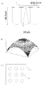
- the irradiation unit 1 is a plurality of light sources in which the light sources 10 for irradiating light having a wavelength of 940 nm are arranged in a square array as shown in FIG. 18 (a). Further, the light emitted by the light source had a butt wing light distribution as shown in FIG. 18 (b) and had a light intensity as shown in FIG. 18 (c) in the distant field. As shown in FIG. 39A, the optical element 2 is a square array of lenses 21 having a pitch of 33 ⁇ m. Further, as shown in FIG. 39 (b), the shape of each lens 21 has the following equation.
- the cross-sectional shape of the boundary portion of the lens which tends to be a singular point when the lens is created by the imprint method, has a parabolic shape with a width of 1.5 ⁇ m, which has a minimum boundary value and is smoothly connected to the lens shape of the above formula. ..
- the material was assumed to be PDMS with a refractive index of 1.53.
- a circular opening 70 having a diameter of 16.5 ⁇ m was used, which was arranged in a square matrix. Further, as shown in FIG. 39 (a), the aperture mask 7 is arranged so that the center of the aperture 70 is the position of the focal point of the lens. Regarding the influence of noise light depending on the presence or absence of the aperture mask 7, a dot pattern without the aperture mask 7 is shown in FIG. 40, and a dot pattern with the aperture mask 7 is shown in FIG. 41. The dot pattern is on a 70 cm ⁇ 70 cm plate 50 cm away from the optical element.
- the optical simulation software BeamPROP manufactured by Synopsys was used for the simulation.
- FIG. 42 (a) shows model 1 without the aperture mask 7.
- the lens period is 10 ⁇ m
- the lens height is 5 ⁇ m
- the shape of the lens is an arc with a diameter of 0.5 ⁇ m.
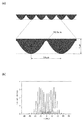
- the light intensity in this case is shown in FIG. 42 (b). It can be seen that a small peak, which is noise light, is generated between the peaks near the center.
- FIG. 43A shows a model 2 in which an aperture mask 7 for shielding the transmitted light from the lens 21 is formed on the bottom side of the boundary portion of the lens 21.
- the width of the aperture mask 7 was set to 1 ⁇ m in accordance with the width of the arc having a diameter of 0.5 ⁇ m.
- the thickness of the shielding portion was set to 0.5 ⁇ m.
- the light intensity in this case is shown in FIG. 43 (b). It can be seen that almost no noise light is generated in the central portion as compared with the model 1 without the aperture mask 7.
- the arcuate portion of the boundary portion is likely to be distorted when created by the imprint method. Therefore, as shown in FIG. 44 (a), the arcuate portion of the lens of the model 1 has a flat shape with a width of 1 ⁇ m, and is used as the model 3.
- an aperture mask 7 that shields the transmitted light from the lens 21 is formed on the bottom side of the boundary portion of the lens 21.
- the width of the aperture mask 7 was set to 1 ⁇ m according to the width of the flat portion.
- the thickness of the shielding portion was set to 0.5 ⁇ m.
- the light intensity in this case is shown in FIG. 44 (b). It can be seen that almost no noise light is generated in the center compared to the model without the aperture mask 7.
- FIG. 45A shows a model 4 in which an aperture mask 7 that shields light from a light source is formed on the surface of the boundary portion of the lens 21.
- the width of the aperture mask 7 was set to 1 ⁇ m so that all the light incident on the arc having a diameter of 0.5 ⁇ m could be shielded.
- the light intensity in this case is shown in FIG. 45 (b). It can be seen that almost no noise light is generated in the central portion as compared with the model 1 without the aperture mask 7.
- the optical element may have a light diffusing portion 8 formed at the boundary portion of the lens to refract the transmitted light to the outside of the irradiation angle of the lens (outside the irradiation range of the dot pattern).
- the shape of the light diffusing portion 8 may be any shape as long as the incident light can be refracted to the outside of the irradiation angle of the lens, and any shape that is easy to manufacture may be selected.
- a lens having a triangular cross-sectional shape due to a plane parallel to the boundary of the lens can be adopted.
- FIG. 46 (a) The effect of noise light due to the presence or absence of the light diffusing unit 8 was simulated.
- the lens has a shape having a light diffusing portion 8 at the boundary portion of the lens used in the simulation 7.
- the light diffusing portion 8 was formed with a width of 1.5 ⁇ m from the boundary around the lens.
- the cross-sectional shape of the light diffusing portion 8 (cross-section parallel to the nearest boundary of the lens) is a similar triangle of aspect 1 having the same width and height of the base. It has an uneven structure arranged side by side.
- the triangles having similar figures were arranged so that the position of the base of the triangle and the position of the bottom of the lens coincided with each other. Others were the same as in Simulation 7.
- FIG. 47 shows a dot pattern when the light diffusing unit 8 is present.
- the lens 21 of the optical element 2 may be manufactured in any way, and can be manufactured by using, for example, an imprint method. Specifically, the material of the lens 21 is coated on the substrate 25 with a predetermined film thickness by a well-known method such as a spin coater (coating step). As the material, any material can be used as long as it can form a lens 21 that transmits light having a wavelength ⁇ , and for example, polydimethylsiloxane (PDMS) can be used.
- PDMS polydimethylsiloxane
- a mold having a pattern inversion pattern in which the lenses 21 are periodically arranged is prepared, and the mold is pressed against the material applied on the substrate 25 to transfer the pattern (imprint process).
- a mold having the inversion pattern of the light diffusing portion 8 may be used together with the pattern.
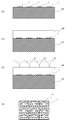
- the aperture mask 7 when forming the aperture mask 7 on the optical element, it has an aperture mask forming step. First, a case where the aperture mask 7 is formed so as to be arranged in the optical path of the noise light of the lens 21 will be described.
- an aperture mask 7 is formed on the substrate 25 to prevent light from transmitting at least at a position separated from the position corresponding to the optical axis of the lens 21 by a predetermined distance (1).
- the aperture mask 7 may be formed by any method, and for example, it may be formed by the following method.
- a resist is applied on a film made of a light-shielding material, and a resist is formed at a position other than the opening portion of the aperture mask by existing techniques such as photolithography and imprint.
- the size of the opening 70 may be formed so as to allow effective light to pass through as much as possible.
- the aperture mask 7 can be formed by etching the light-shielding material with this resist and removing the remaining resist by ashing or the like.
- any material may be used as long as it can block the light to be used, and for example, a metal such as silver, aluminum or chromium oxide or a resin such as black resist can be used.
- a transparent film 26 for adjusting the distance between the lens 21 and the aperture mask 7 is formed.
- the transparent film 26 may be formed in any way, and may be formed by applying a transparent material on the substrate 25 with a predetermined film thickness by, for example, a well-known method such as a spin coater.
- the material may be any material that transmits light having a wavelength of ⁇ , and for example, polydimethylsiloxane (PDMS) can be used.
- PDMS polydimethylsiloxane
- the lens 21 is formed as shown in FIG. 48 (c) (lens forming step).
- the lens may be formed by any method, and for example, the lens 21 may be formed by aligning with the aperture mask 7 and using an existing technique such as an imprint method. In this case, the distance between the lens 21 and the aperture mask 7 is determined by the size of the transparent film 26 and the residual film due to imprinting. In this way, as shown in FIG. 48 (d), the aperture mask 7 integrated with the optical element 2 can be formed. The distance between the lens 21 and the aperture mask 7 can be adjusted only by the size of the residual film by imprinting without forming the transparent film 26.
- the aperture mask 7 when the aperture mask 7 that shields the transmitted light from the lens is formed on the transmitted light side of the lens 21 at the boundary portion, the aperture mask 7 is formed by the following method. do it.
- an aperture mask 7 is formed on the substrate 25 to prevent light from being transmitted to a position corresponding to a lens boundary (aperture mask forming step).
- the aperture mask 7 may be formed by any conventionally known method, and may be formed by, for example, the following method.
- CVD chemical vapor deposition
- a resist is applied on a film made of a light-shielding material, and a resist is formed with a desired width that can block noise light only at the position corresponding to the boundary of the lens by existing techniques such as photolithography and imprint. do.
- the aperture mask 7 can be formed by etching the light-shielding material with this resist and removing the remaining resist by ashing or the like.
- any material may be used as long as it can block the light to be used, and for example, a metal such as silver, aluminum or chromium oxide or a resin such as black resist can be used.
- the lens 21 is formed so that the boundary of the lens 21 is arranged on the aperture mask 7 as shown in FIG. 49 (b) (lens forming step). ..
- the lens may be formed by any method, and for example, the lens 21 may be formed by aligning with the aperture mask 7 and using an existing technique such as an imprint method. As a result, as shown in FIG. 49 (c), the aperture mask 7 integrated with the optical element 2 can be formed.
- the aperture mask 7 that shields the light from the light source is formed on the light source side of the lens 21 at the boundary portion, it can be formed by the following method. good.
- the lens 21 of the optical element may be formed in any way, and existing techniques such as an imprint method may be used.
- a light-shielding material for preventing light from being transmitted is applied to all or part of the lens 21 to form the light-shielding film 27.
- the light-shielding material is removed so that a part of the light-shielding material remains at the position corresponding to the boundary of the lens 21 to form the aperture mask 7 (aperture mask forming step).
- a light-shielding material such as black resist is applied onto the lens 21. If the light-shielding material is etched back by a desired amount by etching, it is possible to form an optical element in which the light-shielding material remains only in the groove portion corresponding to the boundary of the lens 21.
- any material may be used as long as it can block the light to be used and the etching rate with respect to the lens 21 is sufficiently high.
- the sufficiently high etching rate means that the optical characteristics of the lens 21 are not affected.
- Any etching method may be used as long as etch back is possible, and for example, reactive ion etching (RIE) or chemical dry etching (CDE) may be used.
- RIE reactive ion etching
- CDE chemical dry etching
- the irradiation unit 1 has a plurality of light sources 10, even if each light source 10 and the optical element 2 are relatively translated, the number of light sources 10 for each lens 21 of the optical element 2 is the same in a plan view. It is necessary to arrange so as to be. Specifically, assuming that m is a natural number of 1 or more, the irradiation unit regularly uses a plurality of light sources at m times or 1 / m times of the period with respect to any period direction of the lens 21 of the optical element. It is good to arrange in.
- the light source 10 of the irradiation unit 1 may be regularly arranged at a pitch mP k or P k / m with respect to the direction in which the lens 21 of the optical element 2 takes the pitch P k.
- the pitch mP 1 or P 1 / m is preferable.
- m 2
- the pitch of the light source 10 is twice the pitch P 1 of the lens 21 of the optical element 2, that is, 2P 1 .
- P 2 ⁇ in order to satisfy Equation 1 for the smallest pitch P 1 (the size of the short side of the rectangle) and the second smallest pitch P 2 (the size of the long side of the rectangle).
- the distance L 1 between the irradiation unit 1 and the optical element 2 is set. Is preferable, and more preferably It is better to say.
- the light of the irradiation unit 1 does not need to directly irradiate the optical element 2, but may be irradiated through the mirror 3 that reflects the light of the irradiation unit 1.
- the distance L 1 between the irradiation unit 1 and the optical element 2 means a substantial distance.
- the distance L 1 in the case of FIG. 52 is a La + Lb from the distance La and the mirror 3 from the irradiation portion 1 to the mirror 3 which is the sum of the distance Lb to the optical element 2 shown by the arrow.
- the distance L can be adjusted by using the mirror 3. It is also possible to adjust the direction of the light from the light source.
- FIG. 53A is a schematic plan view of the irradiation unit 1 viewed from the optical element 2 side.
- the optical element 2 is a regular arrangement of lenses 21 having a rectangular planar shape.
- a light source 10 arranged in a hexagonal arrangement was used as the irradiation unit 1.
- the arrangement of the light source 10 shown in FIG. 53 (a) can be divided into four as shown in FIG. 53 (b) when decomposed.
- the dot patterns emitted from the arrangements of the light sources 10 at the upper left and lower left and at the upper right and lower right in FIG. 53B are the same, so that they can be identified. Therefore, the arrangement of the light source 10 with respect to the optical element 2 can be substantially classified into the two types shown in FIG. 53 (c).
- the irradiation unit 1 includes a first irradiation unit 1A in which a plurality of light sources 10 irradiating light having a wavelength ⁇ are regularly arranged, and a plurality of light sources 10 irradiating light having a wavelength ⁇ .
- the same light distribution can be realized even if it is composed of the light source 10 of the first irradiation unit 1A and the second irradiation unit 1B which is regularly arranged by shifting the light source 10 in the vertical and horizontal directions by half a cycle.
- the irradiation unit 1 is composed of a first irradiation unit, a second irradiation unit, and a third irradiation unit in which a plurality of light sources 10 for irradiating light having a wavelength ⁇ are regularly arranged, and each irradiation unit is composed of an optical element 2.
- the lens 21 may be arranged so as to be shifted by P k / 3 with respect to the direction in which the pitch P k is taken.
- FIG. 55 (a) shows a case where the optical element 2 uses lenses 21 having a rectangular planar shape in a regular arrangement, and the irradiation unit 1 uses a light source 10 arranged in a hexagonal arrangement. ..
- the irradiation unit may cause the first irradiation unit, the second irradiation unit, and the third irradiation unit to emit light in order at different times.
- the resolution can be tripled by performing three measurements with the light receiving sensor.
- the arrangement of the lenses 21 is a lens connected in the direction of the above-mentioned side, assuming that i is a natural number of 1 or more.
- the 21 columns may be arranged by shifting them by R / i. As a result, the number of emitted dots can be multiplied by i.
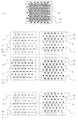
- the irradiation unit 1 is arranged in a hexagonal arrangement so that the light source 10 that irradiates light having a wavelength of 940 nm has a minimum pitch of 21 ⁇ m. Further, the size of the light source 10 is assumed to be 10 ⁇ m. Further, the planar shape of the lens 21 of the optical element 2 is assumed to be a rectangle with a length of 21 ⁇ m and a width of 36.4 ⁇ m. The distance between the irradiation unit 1 and the optical element 2 was set to 1407 ⁇ m. As shown in FIG.
- FIG. 57 (a) when the lenses 21 in adjacent rows of the optical elements 2 are arranged in the same manner, the positions of the light sources 10 with respect to each lens 21 are combined as shown in FIG. 57 (b). Therefore, the number of lights of the light source 10 per lens 21 is two. In this case, the illuminated dot pattern is as shown in FIG. 57 (c).
- FIG. 58 (a) when the lenses 21 in the adjacent rows of the optical elements 2 are arranged so as to be shifted by R / 2, the positions of the light sources 10 with respect to each lens 21 are combined in FIG. 58 (b). ), And the number of lights of the light source 10 per lens 21 is four.
- the number of dots of the illuminated dot pattern is doubled as shown in FIG. 58 (c).
- FIG. 59 (a) when the lenses 21 in the adjacent rows of the optical elements 2 are arranged by shifting them by R / 3, the positions of the light sources 10 with respect to each lens 21 are combined in FIG. 59 (b). ), And the number of lights of the light source 10 per lens 21 is six. In this case, since the light of the light source 10 per lens 21 is tripled, the number of dots of the illuminated dot pattern is tripled as shown in FIG. 59 (c).
- the light of the light source 10 per lens 21 is 2i. It becomes an individual. Therefore, the light of the light source 10 per lens 21 is i times when the rows of adjacent lenses 21 are not shifted at all, and the number of emitted dots is also i times.
- the optical system device is arranged between the diffuser that diffuses the light of the irradiation unit 1 into a predetermined shape, the light source 10, and the diffuser, and transmits a part of the light of the irradiation unit 1.
- a half mirror that partially reflects the light and a mirror that reflects the light reflected by the half mirror 4 to the optical element 2 may be provided.
- optical element 2 according to the present invention can be used not only for irradiating a dot pattern but also for a diffuser application.
- irradiation for a diffuser in which a plurality of light sources 10 for irradiating light having a wavelength ⁇ are arranged in the same manner as the irradiation unit 1 used for irradiating a dot pattern is performed.
- Prepare part 6 The distance L 2 between the diffuser irradiation unit 6 and the optical element 2 is the following equation 2. You just have to meet. As a result, as shown in Simulation 1 and FIGS. 7 to 9 described above, it can be seen that the width of each peak is widened and the unevenness of the light intensity is reduced.
- the distance L 2 is the following formula 3. It is better to meet.
- the optical element 2 may be used in common, or as shown in FIG. 61 (b), the optical element 2a for the dot pattern and the optics for the diffuser. Two of the elements 2b may be used.
- a diffuser irradiation unit 6 in which a plurality of light sources 60 for irradiating light having a wavelength ⁇ are arranged is prepared. Then, assuming that m is a natural number of 1 or more, the diffuser irradiation unit 6 does not make a plurality of light sources 60 m times or 1 / m times the periodic direction of the lens 21 of the optical element 2. All you have to do is arrange them.
- the plurality of light sources 60 of the diffuser irradiation unit 6 may be m times or 1 / m times the cycle.
- the diffuser irradiation unit 6 for the optical element may be rotated with respect to the optical axis direction of the light source 60.
- the arrangement of the plurality of light sources 60 can be shifted with respect to the periodic direction of the lens 21 of the optical element 2 so as not to be m times or 1 / m times the period.
- the rotation angle ⁇ means the angle difference in the direction in which the light source 10 of the diffuser irradiation unit 6 takes the pitch mP k or P k / m with respect to the direction in which the lens 21 of the optical element 2 takes the pitch P k.
- the pitch of the irradiation unit 1 and the pitch of the optical element 2 match (when ⁇ is 0 degrees)
- the angle ⁇ increases, the position of the light source 10 begins to shift.
- the irradiation section was a VCSEL having a hexagonal arrangement with a pitch of 21 ⁇ m, a wavelength of 940 nm, a spread angle (FWHM) of 20 degrees, and an emitter pitch of 10 ⁇ m.
- the optical element was a rectangle with a refractive index of 1.53, a pitch of 21 ⁇ m ⁇ 36.37 ⁇ m, and a FOI of 60 degrees ⁇ 45 degrees.
- the distance between the optical element and the irradiation unit was 1407 ⁇ m.
- the projection position of the dot pattern was 50 cm ahead of the optical element.
- the rotation angle ⁇ with respect to the optical element 2 was set to 0 degree, 1 degree, 5 degree, 10 degree, and 15 degree.
- 66 to 70 are views showing a rotation angle and a dot pattern with respect to the optical element 2.
- the optical simulation software BeamPROP manufactured by Synopsys was used for the simulation.
- the optical element 2 can be used as a diffuser by appropriately adjusting the rotation angle ⁇ of the diffuser irradiation unit 6 with respect to the optical element.
- the third method of using the optical element 2 as a diffuser is a method of increasing the number of dots in the dot pattern to make the irradiated light seemly uniform.
- the planar shape of the lens 21 is a square, rectangle, diamond or parallelogram whose side length is R, as described above.
- the rows of the lenses 21 connected in the direction of the side described above are arranged so as to be shifted by R / i. Then, i may be adjusted so that the number of emitted dots is equal to or higher than the resolution of the light receiving sensor.
- the diffuser formed in this way can be used in combination with the optical system device for irradiating the above-mentioned dot pattern.
- the intensity of the irradiation light is secured by the dot pattern and the distance and shape are measured, and for short-distance objects, the distance and shape are more accurate by irradiating the diffuser light. Can be measured.
- Irradiation unit 1A 1st irradiation unit 1B 2nd irradiation unit 2 Optical element 3 Mirror 4 Half mirror 5 Diffuser type optical element 6 Diffuser irradiation unit 7 Aperture mask 8 Light diffuser 10 Light source 11 Irradiation unit 12 Irradiation unit 13 Irradiator 21 Lens 25 Substrate 60 Light source 70 Aperture
Landscapes
- Physics & Mathematics (AREA)
- General Physics & Mathematics (AREA)
- Optics & Photonics (AREA)
- Engineering & Computer Science (AREA)
- Condensed Matter Physics & Semiconductors (AREA)
- Electromagnetism (AREA)
- Computer Networks & Wireless Communication (AREA)
- Radar, Positioning & Navigation (AREA)
- Remote Sensing (AREA)
- Semiconductor Lasers (AREA)
- Sheets, Magazines, And Separation Thereof (AREA)
- Lenses (AREA)
Priority Applications (3)
| Application Number | Priority Date | Filing Date | Title |
|---|---|---|---|
| US17/924,936 US20230204824A1 (en) | 2020-05-13 | 2020-12-17 | Optical System Device |
| CN202080100825.4A CN115552278B (zh) | 2020-05-13 | 2020-12-17 | 光学系统装置及光学元件制造方法 |
| JP2021521863A JP7061823B2 (ja) | 2020-05-13 | 2020-12-17 | 光学系装置および光学素子製造方法 |
Applications Claiming Priority (4)
| Application Number | Priority Date | Filing Date | Title |
|---|---|---|---|
| JP2020084820 | 2020-05-13 | ||
| JP2020-084820 | 2020-05-13 | ||
| JP2020135464 | 2020-08-08 | ||
| JP2020-135464 | 2020-08-08 |
Publications (1)
| Publication Number | Publication Date |
|---|---|
| WO2021229848A1 true WO2021229848A1 (ja) | 2021-11-18 |
Family
ID=78524437
Family Applications (2)
| Application Number | Title | Priority Date | Filing Date |
|---|---|---|---|
| PCT/JP2020/047275 Ceased WO2021229848A1 (ja) | 2020-05-13 | 2020-12-17 | 光学系装置および光学素子製造方法 |
| PCT/JP2021/018246 Ceased WO2021230324A1 (ja) | 2020-05-13 | 2021-05-13 | 光学系装置および光学素子製造方法 |
Family Applications After (1)
| Application Number | Title | Priority Date | Filing Date |
|---|---|---|---|
| PCT/JP2021/018246 Ceased WO2021230324A1 (ja) | 2020-05-13 | 2021-05-13 | 光学系装置および光学素子製造方法 |
Country Status (4)
| Country | Link |
|---|---|
| US (1) | US20230204824A1 (https=) |
| JP (1) | JP7061823B2 (https=) |
| CN (1) | CN115552278B (https=) |
| WO (2) | WO2021229848A1 (https=) |
Cited By (7)
| Publication number | Priority date | Publication date | Assignee | Title |
|---|---|---|---|---|
| JP2022104454A (ja) * | 2020-12-28 | 2022-07-08 | 株式会社ダイセル | マイクロレンズアレイ、拡散板及び照明装置 |
| WO2023026987A1 (ja) * | 2021-08-25 | 2023-03-02 | Scivax株式会社 | 光学系装置 |
| JPWO2023090435A1 (https=) * | 2021-11-19 | 2023-05-25 | ||
| JPWO2024029616A1 (https=) * | 2022-08-05 | 2024-02-08 | ||
| WO2024143433A1 (ja) * | 2022-12-27 | 2024-07-04 | Scivax株式会社 | 光学系装置 |
| WO2024143498A1 (ja) * | 2022-12-27 | 2024-07-04 | Scivax株式会社 | 光学系装置 |
| WO2025057909A1 (ja) | 2023-09-11 | 2025-03-20 | Scivax株式会社 | 光学系装置 |
Families Citing this family (3)
| Publication number | Priority date | Publication date | Assignee | Title |
|---|---|---|---|---|
| CN217034418U (zh) * | 2022-01-11 | 2022-07-22 | 深圳迈塔兰斯科技有限公司 | 光学系统及包含其的光固化打印系统 |
| JPWO2024128049A1 (https=) * | 2022-12-15 | 2024-06-20 | ||
| WO2024143481A1 (ja) * | 2022-12-27 | 2024-07-04 | Scivax株式会社 | 三次元撮影装置 |
Citations (6)
| Publication number | Priority date | Publication date | Assignee | Title |
|---|---|---|---|---|
| JPH0264501A (ja) * | 1988-08-30 | 1990-03-05 | Sharp Corp | マイクロレンズアレイ及びその製造方法 |
| JP2000298201A (ja) * | 1999-04-14 | 2000-10-24 | Omron Corp | マイクロレンズアレイ |
| JP2002277610A (ja) * | 2001-03-21 | 2002-09-25 | Ricoh Co Ltd | 遮光部付きマイクロレンズ基板の作製方法 |
| JP2005156203A (ja) * | 2003-11-21 | 2005-06-16 | Matsushita Electric Works Ltd | レーザ測距装置 |
| WO2017131585A1 (en) * | 2016-01-26 | 2017-08-03 | Heptagon Micro Optics Pte. Ltd. | Multi-mode illumination module and related method |
| JP2018511034A (ja) * | 2015-01-29 | 2018-04-19 | ヘプタゴン・マイクロ・オプティクス・プライベート・リミテッドHeptagon Micro Optics Pte. Ltd. | パターン化された照射を生成するための装置 |
Family Cites Families (8)
| Publication number | Priority date | Publication date | Assignee | Title |
|---|---|---|---|---|
| US10509147B2 (en) * | 2015-01-29 | 2019-12-17 | ams Sensors Singapore Pte. Ltd | Apparatus for producing patterned illumination using arrays of light sources and lenses |
| KR101945661B1 (ko) * | 2015-03-12 | 2019-02-07 | 주식회사 쿠라레 | 확산판 |
| DE102017217345B4 (de) * | 2017-09-28 | 2019-12-24 | Fraunhofer-Gesellschaft zur Förderung der angewandten Forschung e.V. | Optischer Strahlformer |
| JP7102797B2 (ja) * | 2018-03-12 | 2022-07-20 | 株式会社リコー | 光学装置、これを用いた距離計測装置、及び移動体 |
| US11624832B2 (en) * | 2018-06-08 | 2023-04-11 | Samsung Electronics Co., Ltd. | Illumination device and electronic device including the same |
| US11175010B2 (en) * | 2018-09-20 | 2021-11-16 | Samsung Electronics Co., Ltd. | Illumination device and electronic apparatus including the same |
| WO2020065391A1 (en) * | 2018-09-24 | 2020-04-02 | Ams Sensors Asia Pte, Ltd. | Improved illumination device |
| US11085609B1 (en) * | 2021-02-08 | 2021-08-10 | Himax Technologies Limited | Illumination device |
-
2020
- 2020-12-17 CN CN202080100825.4A patent/CN115552278B/zh active Active
- 2020-12-17 US US17/924,936 patent/US20230204824A1/en active Pending
- 2020-12-17 WO PCT/JP2020/047275 patent/WO2021229848A1/ja not_active Ceased
- 2020-12-17 JP JP2021521863A patent/JP7061823B2/ja active Active
-
2021
- 2021-05-13 WO PCT/JP2021/018246 patent/WO2021230324A1/ja not_active Ceased
Patent Citations (6)
| Publication number | Priority date | Publication date | Assignee | Title |
|---|---|---|---|---|
| JPH0264501A (ja) * | 1988-08-30 | 1990-03-05 | Sharp Corp | マイクロレンズアレイ及びその製造方法 |
| JP2000298201A (ja) * | 1999-04-14 | 2000-10-24 | Omron Corp | マイクロレンズアレイ |
| JP2002277610A (ja) * | 2001-03-21 | 2002-09-25 | Ricoh Co Ltd | 遮光部付きマイクロレンズ基板の作製方法 |
| JP2005156203A (ja) * | 2003-11-21 | 2005-06-16 | Matsushita Electric Works Ltd | レーザ測距装置 |
| JP2018511034A (ja) * | 2015-01-29 | 2018-04-19 | ヘプタゴン・マイクロ・オプティクス・プライベート・リミテッドHeptagon Micro Optics Pte. Ltd. | パターン化された照射を生成するための装置 |
| WO2017131585A1 (en) * | 2016-01-26 | 2017-08-03 | Heptagon Micro Optics Pte. Ltd. | Multi-mode illumination module and related method |
Cited By (10)
| Publication number | Priority date | Publication date | Assignee | Title |
|---|---|---|---|---|
| JP2022104454A (ja) * | 2020-12-28 | 2022-07-08 | 株式会社ダイセル | マイクロレンズアレイ、拡散板及び照明装置 |
| WO2023026987A1 (ja) * | 2021-08-25 | 2023-03-02 | Scivax株式会社 | 光学系装置 |
| JPWO2023090435A1 (https=) * | 2021-11-19 | 2023-05-25 | ||
| WO2023090435A1 (ja) * | 2021-11-19 | 2023-05-25 | Scivax株式会社 | 光学系装置および光学素子製造方法 |
| JP7623743B2 (ja) | 2021-11-19 | 2025-01-29 | Scivax株式会社 | 光学系装置および光学素子製造方法 |
| JPWO2024029616A1 (https=) * | 2022-08-05 | 2024-02-08 | ||
| JP7752436B2 (ja) | 2022-08-05 | 2025-10-10 | Scivax株式会社 | 光学素子、光学系装置および光学系装置の製造方法 |
| WO2024143433A1 (ja) * | 2022-12-27 | 2024-07-04 | Scivax株式会社 | 光学系装置 |
| WO2024143498A1 (ja) * | 2022-12-27 | 2024-07-04 | Scivax株式会社 | 光学系装置 |
| WO2025057909A1 (ja) | 2023-09-11 | 2025-03-20 | Scivax株式会社 | 光学系装置 |
Also Published As
| Publication number | Publication date |
|---|---|
| JP7061823B2 (ja) | 2022-05-02 |
| JPWO2021229848A1 (https=) | 2021-11-18 |
| WO2021230324A1 (ja) | 2021-11-18 |
| CN115552278B (zh) | 2025-03-04 |
| US20230204824A1 (en) | 2023-06-29 |
| CN115552278A (zh) | 2022-12-30 |
Similar Documents
| Publication | Publication Date | Title |
|---|---|---|
| JP7061823B2 (ja) | 光学系装置および光学素子製造方法 | |
| JP6424418B2 (ja) | 光学素子、投影装置および計測装置並びに製造方法 | |
| JP5487592B2 (ja) | レーザー加工方法 | |
| US8469549B2 (en) | Beam shaper | |
| JP7418050B2 (ja) | 光学系装置 | |
| CN108351437B (zh) | 扩散板、扩散板的设计方法、扩散板的制造方法、显示装置、投影装置和照明装置 | |
| JP6186679B2 (ja) | 照明光学系、計測装置及びそれに用いられる回折光学素子 | |
| JP7436369B2 (ja) | ランバート分布を有する光をバットウィング分布に変換するマイクロ構造 | |
| CN114556168A (zh) | 扩散板、显示装置、投影装置以及照明装置 | |
| JP2019139163A (ja) | 拡散板、拡散板の設計方法、表示装置、投影装置及び照明装置 | |
| JP2022536694A (ja) | 格子結合器の片側パターン化を使用した光学接眼レンズ | |
| JP6755076B2 (ja) | 光学素子、投影装置および計測装置 | |
| CN116224607A (zh) | 结构光投射器及3d结构光模组 | |
| KR20210118868A (ko) | 확산판 | |
| JP2020106771A (ja) | 回折光学素子およびこれを用いた光学系装置 | |
| JP2019511748A (ja) | 光強度調整方法 | |
| JP2017097058A (ja) | 光広角照射装置 | |
| CN109856710B (zh) | 一种产生远距离高分辨贝塞尔光束的双胶合轴锥镜及方法 | |
| JP2023152876A (ja) | 拡散板および装置 | |
| WO2023090435A1 (ja) | 光学系装置および光学素子製造方法 | |
| CN216792482U (zh) | 匀光元件 | |
| WO2024143433A1 (ja) | 光学系装置 | |
| US9353929B2 (en) | Beam diffusing module and beam generating system | |
| WO2024106359A1 (ja) | 光学系装置および光学素子 | |
| WO2023190682A1 (ja) | 拡散板および装置 |
Legal Events
| Date | Code | Title | Description |
|---|---|---|---|
| ENP | Entry into the national phase |
Ref document number: 2021521863 Country of ref document: JP Kind code of ref document: A |
|
| 121 | Ep: the epo has been informed by wipo that ep was designated in this application |
Ref document number: 20934946 Country of ref document: EP Kind code of ref document: A1 |
|
| NENP | Non-entry into the national phase |
Ref country code: DE |
|
| 122 | Ep: pct application non-entry in european phase |
Ref document number: 20934946 Country of ref document: EP Kind code of ref document: A1 |
|
| WWG | Wipo information: grant in national office |
Ref document number: 202080100825.4 Country of ref document: CN |