WO2021229714A1 - 電子デバイス検査装置 - Google Patents
電子デバイス検査装置 Download PDFInfo
- Publication number
- WO2021229714A1 WO2021229714A1 PCT/JP2020/019103 JP2020019103W WO2021229714A1 WO 2021229714 A1 WO2021229714 A1 WO 2021229714A1 JP 2020019103 W JP2020019103 W JP 2020019103W WO 2021229714 A1 WO2021229714 A1 WO 2021229714A1
- Authority
- WO
- WIPO (PCT)
- Prior art keywords
- electronic device
- contact
- temperature
- inspection
- electrode
- Prior art date
- Legal status (The legal status is an assumption and is not a legal conclusion. Google has not performed a legal analysis and makes no representation as to the accuracy of the status listed.)
- Ceased
Links
Images




Classifications
-
- G—PHYSICS
- G01—MEASURING; TESTING
- G01R—MEASURING ELECTRIC VARIABLES; MEASURING MAGNETIC VARIABLES
- G01R1/00—Details of instruments or arrangements of the types included in groups G01R5/00 - G01R13/00 and G01R31/00
- G01R1/02—General constructional details
- G01R1/06—Measuring leads; Measuring probes
- G01R1/067—Measuring probes
- G01R1/06711—Probe needles; Cantilever beams; "Bump" contacts; Replaceable probe pins
- G01R1/06755—Material aspects
-
- G—PHYSICS
- G01—MEASURING; TESTING
- G01R—MEASURING ELECTRIC VARIABLES; MEASURING MAGNETIC VARIABLES
- G01R31/00—Arrangements for testing electric properties; Arrangements for locating electric faults; Arrangements for electrical testing characterised by what is being tested not provided for elsewhere
- G01R31/26—Testing of individual semiconductor devices
- G01R31/2601—Apparatus or methods therefor
-
- G—PHYSICS
- G01—MEASURING; TESTING
- G01R—MEASURING ELECTRIC VARIABLES; MEASURING MAGNETIC VARIABLES
- G01R31/00—Arrangements for testing electric properties; Arrangements for locating electric faults; Arrangements for electrical testing characterised by what is being tested not provided for elsewhere
- G01R31/28—Testing of electronic circuits, e.g. by signal tracer
- G01R31/2851—Testing of integrated circuits [IC]
- G01R31/2886—Features relating to contacting the IC under test, e.g. probe heads; chucks
Definitions
- This application relates to an electronic device inspection device.
- an inspection device in which a contact provided at the tip of an arm extending toward an electrode is actively moved toward the electrode by deformation of the arm (see, for example, Patent Document 1).
- the present application discloses a technique for solving the above-mentioned problems, and aims to obtain an electronic device inspection device capable of efficiently and accurately inspecting an electronic device.
- the electronic device inspection device disclosed in the present application is a holding mechanism that positions and holds electrodes arranged in the electronic device, is formed in a long thin plate shape with a shape memory alloy, one end side is fixed to the holding mechanism, and the other end.
- the other end is provided with a contact whose side has a spiral shape at the first temperature and the spiral expands at the second temperature, and a measuring unit for measuring the electronic device by energizing the electrode through the contact.
- the axis of the side spiral is parallel to the plane of the positioned electrode and at the second temperature forms a contact region along the longitudinal direction between the other end and the positioned electrode. It is characterized by doing.
- the contacts are configured to form contacts along the electrode surface, the electronic device can be inspected efficiently and accurately.
- 1A and 1B are a block diagram showing the configuration of the electronic device inspection apparatus according to the first embodiment, and a schematic diagram showing a shape change with a temperature change of the contactor, respectively. It is a schematic diagram which shows the inspection table part for demonstrating the structure of the electronic device inspection apparatus which concerns on Embodiment 1 in the form of a three-sided view.
- 3A and 3B are a perspective view of an inspection table portion for explaining the configuration of the electronic device inspection apparatus according to the first embodiment, and a schematic view shown in a three-view format.
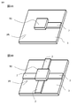
- 4A and 4B are perspective views for explaining the shapes of inspection tables having different arrangements of contacts in the electronic device inspection apparatus according to the first embodiment.
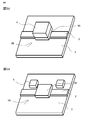
- 5A and 5B are perspective views of an inspection table portion for explaining the configuration of the electronic device inspection apparatus according to the first modification and the second modification of the first embodiment, respectively.
- 6A and 6B are a perspective view of an inspection table portion for explaining the configuration of the electronic device inspection apparatus according to the second embodiment, and a schematic view shown in a three-view format.
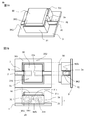
- 7A and 7B are a perspective view of an inspection table portion for explaining the configuration of the electronic device inspection apparatus according to the third embodiment, and a schematic view shown in a three-view format. It is a block diagram which shows the hardware composition of the control part of the electronic device inspection apparatus which concerns on each embodiment.
- Embodiment 1. 1 to 3 are for explaining the electronic device inspection apparatus according to the first embodiment, and FIG. 1 is an inspection table portion on which an electronic device as an inspection product is placed as a configuration of the electronic device inspection apparatus.
- FIG. 1A is a block diagram including a schematic drawing of the above, and a schematic diagram (FIG. 1B) showing a shape change accompanying a temperature change of a contactor in contact with an electrode of an electronic device.
- FIG. 2 is a schematic view showing the inspection table portion in a trigonometric three-view format.
- FIG. 3 is a perspective view (FIG. 3A) of the inspection table portion in a state where the contactor is deformed so as to be in contact with the electrode, and a schematic view (FIG. 3B) shown in a three-view format.
- FIG. 4 and 5 are for explaining the electronic device inspection apparatus according to the application example of the first embodiment, and FIG. 4 shows an example in which the number of contacts is changed, and one contact is shown. It is a perspective view (FIG. 4A) of the inspection table in which the four contacts are arranged, and is a perspective view (FIG. 4B) of the inspection table in which four contacts are arranged.
- FIG. 5 is a perspective view (FIG. 5A) of the inspection table portion of the electronic device inspection device according to the first modification and a perspective view (FIG. 5B) of the inspection table portion of the electronic device inspection device according to the second modification.
- the electronic device inspection device 10 is a mechanism unit having a contact 2 that forms a contact point with an electrode in order to measure the electrical characteristics of the semiconductor device 90 which is an inspection product. 1 and a control unit 6 for controlling a measurement operation are provided.
- An electrode (not shown) is formed on one surface (electrode arrangement surface 90fe: FIG. 2) of an electronic device such as a semiconductor device 90, and by energizing this electrode, measurement of various electrical characteristics is performed. It is configured in.
- the mechanism unit 1 has a contactor 2 and an inspection table 3 to which one end (base 2b) of the contactor 2 is fixed and, for example, a jig (not shown) for holding the semiconductor device 90 is attached.
- the portion for fixing the contact 2 is made of an insulating material such as an insulating substrate, and each contact 2 is provided with a terminal 3t for connecting to the wiring from the measuring unit 61. Further, as described in a modification described later, an instrument for temperature control or fixing of the semiconductor device 90 may be provided.
- the contact 2 is made of a shape memory alloy such as a nickel titanium alloy and is formed in the shape of a long thin plate. Then, as shown in FIG. 1B, one end side is fixed to the upper surface 3ft of the inspection table 3 and the other end side is reversibly changed from a spiral shape to a flat shape or a curved shape in the opposite direction due to a temperature change. It is composed of a variable portion 2a that changes and forms a contact point with the above-mentioned electrode.
- the base portion 2b is fixed to the upper surface 3ft with the axis of the spiral parallel to the electrode placement surface 90fe so that the spiral variable portion 2a rises from the surface 3ft toward the electrode placement surface 90fe. ing. That is, the base portion 2b is fixed to the upper surface 3ft away from the electrode arranging surface 90fe so that the variable portion 2a swirls in the direction approaching the electrode arranging surface 90fe. At that time, with respect to the electrode arrangement surface 90fe of the positioned semiconductor device 90, the side of the spiral variable portion 2a close to the electrode arrangement surface 90fe is directed from the inside to the outside in the direction toward the free end 2ae. It is fixed to the inspection table 3. As a result, when the spiral of the variable portion 2a develops due to the temperature change, the free end 2ae faces the outside of the electrode arrangement surface 90fe.
- the length of the spiral portion needs to be long enough to connect even if there is a gap between the contact 2 and the electrode surface when the shape is restored. For example, in consideration of the manufacturing error in the height direction between the electrode surface and the contactor 2, it is necessary to have a length for securing the deformation amount and the contact area required for generating the pressing force due to the elastic deformation described later.
- the control unit 6 outputs a measurement unit 61 that measures electrical characteristics by passing a current through the inspection product, an inspection control unit 64 that controls the entire inspection operation, an inspection result management unit 65 that manages inspection results, and an inspection result. It includes an inspection result output unit 66 and a data storage unit 67 for storing data. Further, for example, a temperature adjusting unit 63 for changing the shape of the contact 2 and a holding mechanism control unit 62 for controlling a mechanism for holding the inspection product may be provided, which will be described in a modification described later.
- the semiconductor device 90 which is an inspection product
- the contactor 2 at room temperature has a spiral shape, and as described above, the side close to the electrode arrangement surface 90fe is inside in the direction toward the free end 2ae. Towards the outside.
- the semiconductor device 90 uses a jig (not shown) with respect to the inspection table 3 without being interfered by the contactor 2. It can be easily positioned.
- variable portion 2a expands from the spiral shape, and as shown in FIG. 3, the portion of the electrode arrangement surface 90fe that hits an electrode (not shown) is along the electrode surface. It is deformed into a U shape and forms a contact region Rc with the electrode surface.
- the originally flat portion elastically deforms and acts as a spring, so that the variable portion 2a generates a pressing force on the electrode surface and is good between the contact region Rc and the surface. Electrical connection is possible.
- variable portion 2a is deformed along the inclined electrode surface and a pressing force can be applied, so that the variable portion 2a can be efficiently and accurately installed. Allows inspection of electronic devices.
- a contact is formed using a bimetal that deforms due to the difference in the coefficient of linear expansion, it is possible to change between spiral and flat depending on the temperature.
- it acts as a spring due to the change in curvature, it becomes difficult to deform in the direction intersecting the bending direction, and there is a possibility of uneven contact with the tilted electrode surface. It is difficult to form Rc.
- the contactor 2 formed of the shape memory alloy can be deformed not only in the bending direction but also in the direction intersecting the bending direction, and good contact is possible by the deformation along the electrode surface. It becomes. Therefore, the contact resistance is small, accurate measurement can be performed, and the pressure is dispersed, so that the electrode surface of the semiconductor device 90 can be suppressed from being damaged.
- the normal temperature is spiral and the high temperature recovers flat
- the shape is not limited to this.
- a shape memory alloy that recovers its shape at room temperature is used for the contactor 2
- the above-mentioned spring does not act, so that the contactor 2 does not cause interference such as pushing back. , Can be positioned accurately. Then, by cooling the contact 2 to a temperature at which the shape is restored, a good contact region Rc is formed, and accurate inspection becomes possible.
- the number of contacts 2 installed on the inspection table 3 is not limited to two, and as shown in FIG. 4 (FIGS. 4A and 4B), one or four contacts, a test piece, or a test. Any number may be used according to the content. On the other hand, considering the above-mentioned interference by the contacts 2, the effect of facilitating the positioning according to the present application is exhibited as the number of contacts 2 increases.
- a stopper, a pressurizing tool, or a movement preventing tool 4 such as a heavy stone is installed in order to prevent the semiconductor device 90 from being dragged and moving when the contact 2 recovers its shape. You may do so.
- the inspection control unit 64 may monitor the progress of the measurement by the measurement unit 61, and the holding mechanism control unit 62 may control the drive and release of the movement preventive tool 4. With this configuration, the contact pressure between the recovered contact 2 and the semiconductor device 90 increases, so that the electrical connection becomes more reliable, and replacement with the next inspection body can be performed quickly. Therefore, the inspection efficiency is high.
- the mechanism for changing the temperature of the contact 2 can be realized by raising the atmosphere temperature by bringing a heat source such as a dryer closer to the contact 2 or putting the test piece in a constant temperature bath or the like. good.
- a thermomodule 5 such as a Pelche element may be arranged in the vicinity of the contactor 2.
- the inspection control unit 64 monitors the progress of the measurement by the measurement unit 61, and causes the temperature adjustment unit 63 to control the temperature rise and cooling by the thermo module 5, the on / off of the dryer, or the loading and unloading of the dryer into the constant temperature bath. You may do so.
- the inspection is performed at a high temperature, it is suitable because the temperature at the time of inspection can be accurately controlled by making the temperature rise and cooling into a process.
- FIG. 6 is for explaining the electronic device inspection apparatus according to the second embodiment, and is a perspective view (FIG. 6A) of an inspection table portion and a schematic view (FIG. 6B) shown in a three-view format.
- the movement of the contact is the same as described in the first embodiment, and the form of the entire electronic device inspection device and the contact itself is shown in FIG. 1, when the contact recovers its shape and forms a contact region.
- FIG. 3B is used for the shape of.
- the electronic device inspection device 10 has a recess from the mounting surface 3ft1 on which the semiconductor device 90 is mounted on the inspection table 3, and a groove portion 3g corresponding to each of the contacts 2.
- the base portion 2b of the contact 2 is fixed on the bottom surface 3ft2 of the groove portion 3g, and the contactor 2 is placed between the mounting surface 3ft1 and the bottom surface 3ft2 when the variable portion 2a has a spiral shape. Contained inside.
- the wall surface of the groove 3g portion is also formed of an insulating material, and contacts 2 connected to terminals 3t (not shown) are arranged therein.
- the variable portion 2a is not in contact with the contactor 2 and is not electrically connected in the spiral state.
- the contact 2 is deformed along the electrode surface of the semiconductor device 90 and is electrically connected by forming the contact region Rc, as in the first embodiment.
- the semiconductor device 90 Since the semiconductor device 90 is installed on the mounting surface 3ft1 of the inspection table 3 itself, the parallelism between the electrode arrangement surface 90fe and the bottom surface 3ft2 is higher than in the case of using a jig or the like, and the shape of the contact 2 is restored. The accuracy of electrical connection is improved. Further, the contact 2 can be electrically connected to the electrode of the semiconductor device 90 by raising the temperature of the contact 2 at an arbitrary timing. Therefore, when the semiconductor device 90 is installed, it is possible to suppress the generation of electrostatic discharge due to the charging of the human body, and it is possible to protect the semiconductor device 90.
- the contact 2 since the contact 2 is housed in the groove 3 g, the side surface of the groove 3 g acts as a guide, and when the contact 2 recovers its shape, it deforms along the side surface. Therefore, if the width of the groove 3g is aligned with the width of the electrode of the semiconductor device 90, the contact 2 can be prevented from being displaced from the electrode when it is deformed, and can be more reliably electrically connected. Further, since the semiconductor device 90 is in contact with the mounting surface 3ft1, there is no physical load when pressing the contactor 2 at the time of installation, and even when the semiconductor device 90 generates heat, the heat dissipation of the inspection table 3 is high. Therefore, the thermal load on the contact 2 and the semiconductor device 90 is reduced. This is particularly effective when an electronic device with a large calorific value is used as an inspection product.
- the movement preventive device 4 and the thermo module 5 may be provided as described in the first modification and the second modification of the first embodiment.
- FIG. 7 is for explaining the electronic device inspection apparatus according to the third embodiment, and is a perspective view (FIG. 7A) of an inspection table portion and a schematic view (FIG. 7B) shown in a three-view format. Also in the third embodiment, the movement of the contactor is the same as that described in the first embodiment, and the form of the entire electronic device inspection device and the contactor itself is shown in FIG. 1, and the shape of the contactor is restored.
- FIG. 3B is used for the shape when the contact region is formed.
- the electronic device inspection device 10 is provided with a socket 31 into which the semiconductor device 90 is fitted in the inspection table 3.
- the socket 31 has a groove portion 3g for accommodating the contact 2 described in the second embodiment, a mounting surface 3ft1 on which the semiconductor device 90 is mounted, and supports four side portions of the rectangular plate-shaped semiconductor device 90.
- a frame-shaped portion 31c is formed.
- the wall surface of the groove portion 3g provided in the socket 31 is also formed of an insulating material, and contactors 2 connected to terminals 3t (not shown) are arranged therein.
- the variable portion 2a is not in contact with the contactor 2 and is not electrically connected in the spiral state.
- the contact 2 is deformed along the electrode surface of the semiconductor device 90 and is electrically connected by forming the contact region Rc, as in the first embodiment. NS.
- the four side portions adjacent to the electrode arranging surface 90fe in the rectangular plate-shaped semiconductor device 90 are supported by the frame-shaped portion 31c, positioning in a direction parallel to the electrode arranging surface 90fe can be easily performed, and the above-mentioned It is possible to prevent misalignment even when a force is applied during shape recovery.
- the parallelism between the electrode arrangement surface 90fe and the bottom surface 3ft2 is high, and the accuracy of electrically connecting the contactor 2 when the shape is restored is improved.
- the contact 2 can be electrically connected to the electrode of the semiconductor device 90 by raising the temperature of the contact 2 at an arbitrary timing. Therefore, when the semiconductor device 90 is installed, it is possible to suppress the generation of electrostatic discharge due to the charging of the human body, and it is possible to protect the semiconductor device 90.
- the contact 2 since the contact 2 is housed in the groove 3 g, the side surface of the groove 3 g acts as a guide, and when the contact 2 recovers its shape, it deforms along the side surface. Therefore, if the width of the groove 3g is aligned with the width of the electrode of the semiconductor device 90, the contact 2 can be prevented from being displaced from the electrode when it is deformed, and can be more reliably electrically connected. Further, since the semiconductor device 90 is in contact with the mounting surface 3ft1, there is no physical load when pressing the contactor 2 at the time of installation, and even when the semiconductor device 90 generates heat, the frame-shaped portion 31c also serves as a heat dissipation path.
- the heat dissipation is higher than that of the second embodiment, and the thermal load on the contact 2 and the semiconductor device 90 is reduced. This is particularly effective when an electronic device with a large calorific value is used as an inspection product.
- the socket 31 is detachably fixed to the inspection table 3 by screwing or the like, so that even if the semiconductor device 90 is burnt out, other parts can be reused by replacing the socket 31.
- the contacts 2 come into contact with each other when the shape changes, and an unintended portion becomes conductive, which makes accurate inspection impossible. Can be considered.
- the partition 3s that partitions the groove 3g is provided, the contacts 2 do not come into contact with each other and become conductive in the process of changing the shape.
- the movement preventing tool 4 and the thermo module 5 may be provided as described in the first modification and the second modification of the first embodiment.
- the portion that executes the calculation or control of the control unit 6 is a hardware composed of the processor 601 and the storage device 602 as in the example shown in FIG. It can be described as wear 60.
- the storage device 602 includes a volatile storage device such as a random access memory (not shown) and a non-volatile auxiliary storage device such as a flash memory. Further, the auxiliary storage device of the hard disk may be provided instead of the flash memory.
- the processor 601 executes the program input from the storage device 602. In this case, the program is input from the auxiliary storage device to the processor 601 via the volatile storage device. Further, the processor 601 may output data such as a calculation result to the volatile storage device of the storage device 602, or may store the data in the auxiliary storage device via the volatile storage device.
- variable portion 2a has been shown to extend toward the outside of the electrode arrangement surface 90fe of the semiconductor device 90, but the present invention is not limited to this, and the variable portion 2a may be arranged so as to extend toward the inside. Further, a case where the variable portion 2a forms a spiral shape and is spaced from the electrode is shown as a preferable example, but it is not always necessary to space the variable portions 2a, and they are in contact with each other unless an excessive repulsive force is generated. You may.
- the holding mechanism for positioning and holding the electrodes arranged in the electronic device (semiconductor device 90), and the shape memory alloy are long. It is formed in the shape of a thin plate, one end side (base 2b) is fixed to the holding mechanism (upper surface 3ft or bottom surface 3ft2), and the other end side (variable part 2a) forms a spiral shape at the first temperature (for example, normal temperature).
- the axis of the spiral on the other end side is parallel to the positioned electrode surface (electrode arrangement surface 90fe or electrode surface), and at the second temperature, is parallel to the other end side (variable portion 2a). Since the contact region Rc along the long direction is formed between the positioned electrode and the electrode, a contact with the contact 2 is formed along the electrode surface to form an electronic device (semiconductor device 90). It can be inspected efficiently and accurately.
- the contact 2 is configured so that the other end side (variable portion 2a) faces the positioned electrode at a distance at the first temperature, the contact 2 will not be interfered with by the contact 2.
- the electronic device semiconductor device 90
- semiconductor device 90 can be accurately positioned.
- a temperature adjusting unit 63 (and a thermo module 5) for adjusting the temperature of the contact 2 and a control unit (inspection control unit 64) for controlling the operation of the measuring unit 61 in conjunction with the operation of the temperature adjusting unit 63 are provided. If the temperature is set to the above, the contact with the contact 2 is measured in a good state, so that more efficient and accurate inspection can be performed.
- the holding mechanism includes a support surface (mounting surface 3ft1) that supports the surface (electrode arrangement surface 90fe) on which the electrodes of the electronic device (semiconductor device 90) are arranged, and a support surface (mounting surface 3ft1). ), And a groove 3g to which one end (base 2b) of the contact 2 is fixed is provided on the bottom surface 3ft2. It will not be deformed by touching it. Further, the groove portion 3g serves as a guide, and the contact 2 can be smoothly deformed.
- the holding mechanism (inspection table 3) has a frame-shaped portion 31c surrounding the electronic device (semiconductor device 90) in a direction parallel to the surface (electrode arrangement surface 90fe) on which the electrodes of the electronic device (semiconductor device 90) are arranged. If the electronic device (semiconductor device 90) is configured to be provided, the electronic device (semiconductor device 90) can be easily positioned and misalignment can be prevented.
- the holding mechanism (inspection table 3) is provided with a partition 3s in which a plurality of contacts 2 are adjacent to each other along the longitudinal direction and partition between the adjacent contacts 2, a short circuit between the contacts 2 can be caused. Can be prevented.
- a restraining mechanism for restraining the movement of the electronic device (semiconductor device 90) in a direction away from the contact 2
- the electronic device can be pressed by the contact 2.
- the contact state with the contactor 2 can be kept good.
- Mechanism part 10: Electronic device inspection device, 2: Contact, 2a: Variable part, 3: Inspection table (holding mechanism), 31: Socket, 31c: Frame-shaped part, 3ft: Top surface, 3ft 1: Mounting surface (Support surface), 3ft2: Bottom surface, 3g: Groove part, 3s: Partition 4: Movement prevention device (stop mechanism), 5: Thermo module (temperature control unit), 6: Control unit, 61: Measurement unit, 62: Holding Mechanism control unit, 63: Temperature control unit, 64: Inspection control unit, 65: Inspection result management unit, 90: Semiconductor device (electronic device), 90fe: Electrode arrangement surface, Rc: Contact area.
Landscapes
- Physics & Mathematics (AREA)
- General Physics & Mathematics (AREA)
- Testing Of Individual Semiconductor Devices (AREA)
- Measuring Leads Or Probes (AREA)
- Tests Of Electronic Circuits (AREA)
Priority Applications (4)
| Application Number | Priority Date | Filing Date | Title |
|---|---|---|---|
| CN202080100563.1A CN115552259A (zh) | 2020-05-13 | 2020-05-13 | 电子器件检查装置 |
| PCT/JP2020/019103 WO2021229714A1 (ja) | 2020-05-13 | 2020-05-13 | 電子デバイス検査装置 |
| JP2022522165A JP7203283B2 (ja) | 2020-05-13 | 2020-05-13 | 電子デバイス検査装置 |
| US17/907,639 US12123906B2 (en) | 2020-05-13 | 2020-05-13 | Electronic device inspection apparatus |
Applications Claiming Priority (1)
| Application Number | Priority Date | Filing Date | Title |
|---|---|---|---|
| PCT/JP2020/019103 WO2021229714A1 (ja) | 2020-05-13 | 2020-05-13 | 電子デバイス検査装置 |
Publications (1)
| Publication Number | Publication Date |
|---|---|
| WO2021229714A1 true WO2021229714A1 (ja) | 2021-11-18 |
Family
ID=78525534
Family Applications (1)
| Application Number | Title | Priority Date | Filing Date |
|---|---|---|---|
| PCT/JP2020/019103 Ceased WO2021229714A1 (ja) | 2020-05-13 | 2020-05-13 | 電子デバイス検査装置 |
Country Status (4)
| Country | Link |
|---|---|
| US (1) | US12123906B2 (https=) |
| JP (1) | JP7203283B2 (https=) |
| CN (1) | CN115552259A (https=) |
| WO (1) | WO2021229714A1 (https=) |
Citations (9)
| Publication number | Priority date | Publication date | Assignee | Title |
|---|---|---|---|---|
| JPH0233366U (https=) * | 1988-08-29 | 1990-03-02 | ||
| JPH0494576U (https=) * | 1990-12-28 | 1992-08-17 | ||
| JPH06231845A (ja) * | 1992-12-08 | 1994-08-19 | Mitsubishi Electric Corp | 半導体装置用ソケット |
| JPH1073616A (ja) * | 1996-08-29 | 1998-03-17 | Nec Kyushu Ltd | プローブカード |
| JPH10510923A (ja) * | 1994-12-19 | 1998-10-20 | フォード モーター カンパニー | 半導体のダイをテストする方法および装置 |
| JP2000315555A (ja) * | 1999-04-28 | 2000-11-14 | Nec Corp | 半導体パッケージ用ソケット |
| JP2002231399A (ja) * | 2001-02-02 | 2002-08-16 | Fujitsu Ltd | 半導体装置試験用コンタクタ及びその製造方法 |
| JP2008039502A (ja) * | 2006-08-03 | 2008-02-21 | Alps Electric Co Ltd | 接触子およびその製造方法 |
| JP2017204532A (ja) * | 2016-05-10 | 2017-11-16 | 株式会社リコー | プローブカード、ウェハ検査装置および測定方法 |
Family Cites Families (9)
| Publication number | Priority date | Publication date | Assignee | Title |
|---|---|---|---|---|
| JPS60190876A (ja) * | 1984-03-09 | 1985-09-28 | Sharp Corp | 印刷配線基板の検査装置 |
| JPH07193363A (ja) * | 1993-12-27 | 1995-07-28 | Mitsubishi Electric Corp | 電子装置及び電子装置の電極リード接続方法 |
| US6724203B1 (en) * | 1997-10-30 | 2004-04-20 | International Business Machines Corporation | Full wafer test configuration using memory metals |
| JP2002313855A (ja) | 2001-04-10 | 2002-10-25 | Sekisui Chem Co Ltd | 電子回路デバイスの検査装置及び検査方法 |
| JP2004164916A (ja) * | 2002-11-11 | 2004-06-10 | Sumitomo Wiring Syst Ltd | ワイヤーハーネス配線検査用の検査コネクタ |
| JP4041831B2 (ja) * | 2006-05-15 | 2008-02-06 | 日本電産リード株式会社 | 基板検査用治具及びこの治具における接続電極部の電極構造 |
| JP2008060510A (ja) * | 2006-09-04 | 2008-03-13 | Alps Electric Co Ltd | 半導体チップ搭載回路の製造方法および実装回路 |
| JP5156973B1 (ja) * | 2012-08-24 | 2013-03-06 | 株式会社クローバーテクノロジー | 異方導電性部材 |
| KR101998297B1 (ko) * | 2018-01-03 | 2019-07-09 | 최진식 | 형상기억합금을 이용한 전기 커넥터 |
-
2020
- 2020-05-13 JP JP2022522165A patent/JP7203283B2/ja active Active
- 2020-05-13 US US17/907,639 patent/US12123906B2/en active Active
- 2020-05-13 WO PCT/JP2020/019103 patent/WO2021229714A1/ja not_active Ceased
- 2020-05-13 CN CN202080100563.1A patent/CN115552259A/zh active Pending
Patent Citations (9)
| Publication number | Priority date | Publication date | Assignee | Title |
|---|---|---|---|---|
| JPH0233366U (https=) * | 1988-08-29 | 1990-03-02 | ||
| JPH0494576U (https=) * | 1990-12-28 | 1992-08-17 | ||
| JPH06231845A (ja) * | 1992-12-08 | 1994-08-19 | Mitsubishi Electric Corp | 半導体装置用ソケット |
| JPH10510923A (ja) * | 1994-12-19 | 1998-10-20 | フォード モーター カンパニー | 半導体のダイをテストする方法および装置 |
| JPH1073616A (ja) * | 1996-08-29 | 1998-03-17 | Nec Kyushu Ltd | プローブカード |
| JP2000315555A (ja) * | 1999-04-28 | 2000-11-14 | Nec Corp | 半導体パッケージ用ソケット |
| JP2002231399A (ja) * | 2001-02-02 | 2002-08-16 | Fujitsu Ltd | 半導体装置試験用コンタクタ及びその製造方法 |
| JP2008039502A (ja) * | 2006-08-03 | 2008-02-21 | Alps Electric Co Ltd | 接触子およびその製造方法 |
| JP2017204532A (ja) * | 2016-05-10 | 2017-11-16 | 株式会社リコー | プローブカード、ウェハ検査装置および測定方法 |
Also Published As
| Publication number | Publication date |
|---|---|
| US20230131641A1 (en) | 2023-04-27 |
| US12123906B2 (en) | 2024-10-22 |
| JP7203283B2 (ja) | 2023-01-12 |
| CN115552259A (zh) | 2022-12-30 |
| JPWO2021229714A1 (https=) | 2021-11-18 |
Similar Documents
| Publication | Publication Date | Title |
|---|---|---|
| JP5796933B2 (ja) | プローブカードアセンブリ | |
| US7928749B2 (en) | Vertical probe comprising slots and probe card for integrated circuit devices using the same | |
| KR20010024447A (ko) | 적응성 있는 방열 장치를 구비한 번인 보드 | |
| JP2003059602A (ja) | 半導体装置用ソケット | |
| JP2005233858A (ja) | プローブカード | |
| US20050156613A1 (en) | Probe card | |
| KR20170022414A (ko) | 접속 구조체 및 접속 구조체 모듈, 및 이를 이용하는 프로브 카드 어셈블리 및 웨이퍼 테스트 장치 | |
| CN102221634B (zh) | 电子组件接触器、用于测试电子组件的装置及方法 | |
| JP6360671B2 (ja) | 電子コンポーネントの高電流検査のための検査ソケットのための接触ばね | |
| US7518386B2 (en) | Probe card having a leaf spring | |
| WO2021229714A1 (ja) | 電子デバイス検査装置 | |
| US7081005B2 (en) | Electric-connection testing device | |
| US11802909B2 (en) | Compliant ground block and testing system having compliant ground block | |
| JP2011501116A (ja) | プローブ保持装置 | |
| JP6137994B2 (ja) | デバイス検査方法 | |
| JP4408690B2 (ja) | 半導体パッケージのテストシステム及びテスト方法 | |
| KR101976028B1 (ko) | 탄성에 의해 완충작용을 수행하면서 쇼트 발생을 방지할 수 있는 반도체 소켓용 접촉핀 | |
| JP2010043957A (ja) | プローブカード | |
| US9921625B1 (en) | Chassis structure capable of sensing temperature of media storage device | |
| JP4642603B2 (ja) | プローブカード | |
| KR20230087508A (ko) | 히트 싱크 유닛, ic 소켓, 반도체 패키지의 제조방법 및 반도체 패키지 | |
| WO2021153061A1 (ja) | 検査用ソケット | |
| JP4056983B2 (ja) | プローブカード | |
| US20080299792A1 (en) | Burn-in socket having loading plate with uneven seating surface | |
| JP2024156428A (ja) | 検査治具および試験装置 |
Legal Events
| Date | Code | Title | Description |
|---|---|---|---|
| 121 | Ep: the epo has been informed by wipo that ep was designated in this application |
Ref document number: 20934911 Country of ref document: EP Kind code of ref document: A1 |
|
| ENP | Entry into the national phase |
Ref document number: 2022522165 Country of ref document: JP Kind code of ref document: A |
|
| NENP | Non-entry into the national phase |
Ref country code: DE |
|
| 122 | Ep: pct application non-entry in european phase |
Ref document number: 20934911 Country of ref document: EP Kind code of ref document: A1 |