WO2021229374A1 - 半導体装置 - Google Patents
半導体装置 Download PDFInfo
- Publication number
- WO2021229374A1 WO2021229374A1 PCT/IB2021/053820 IB2021053820W WO2021229374A1 WO 2021229374 A1 WO2021229374 A1 WO 2021229374A1 IB 2021053820 W IB2021053820 W IB 2021053820W WO 2021229374 A1 WO2021229374 A1 WO 2021229374A1
- Authority
- WO
- WIPO (PCT)
- Prior art keywords
- insulator
- conductor
- oxide
- transistor
- circuit
- Prior art date
- Legal status (The legal status is an assumption and is not a legal conclusion. Google has not performed a legal analysis and makes no representation as to the accuracy of the status listed.)
- Ceased
Links
Images









Classifications
-
- G—PHYSICS
- G06—COMPUTING OR CALCULATING; COUNTING
- G06F—ELECTRIC DIGITAL DATA PROCESSING
- G06F11/00—Error detection; Error correction; Monitoring
- G06F11/07—Responding to the occurrence of a fault, e.g. fault tolerance
- G06F11/14—Error detection or correction of the data by redundancy in operations
- G06F11/1402—Saving, restoring, recovering or retrying
- G06F11/1415—Saving, restoring, recovering or retrying at system level
- G06F11/1441—Resetting or repowering
-
- H—ELECTRICITY
- H10—SEMICONDUCTOR DEVICES; ELECTRIC SOLID-STATE DEVICES NOT OTHERWISE PROVIDED FOR
- H10D—INORGANIC ELECTRIC SEMICONDUCTOR DEVICES
- H10D88/00—Three-dimensional [3D] integrated devices
-
- G—PHYSICS
- G06—COMPUTING OR CALCULATING; COUNTING
- G06F—ELECTRIC DIGITAL DATA PROCESSING
- G06F21/00—Security arrangements for protecting computers, components thereof, programs or data against unauthorised activity
- G06F21/30—Authentication, i.e. establishing the identity or authorisation of security principals
- G06F21/31—User authentication
- G06F21/34—User authentication involving the use of external additional devices, e.g. dongles or smart cards
-
- G—PHYSICS
- G06—COMPUTING OR CALCULATING; COUNTING
- G06F—ELECTRIC DIGITAL DATA PROCESSING
- G06F7/00—Methods or arrangements for processing data by operating upon the order or content of the data handled
- G06F7/38—Methods or arrangements for performing computations using exclusively denominational number representation, e.g. using binary, ternary, decimal representation
- G06F7/48—Methods or arrangements for performing computations using exclusively denominational number representation, e.g. using binary, ternary, decimal representation using non-contact-making devices, e.g. tube, solid state device; using unspecified devices
- G06F7/544—Methods or arrangements for performing computations using exclusively denominational number representation, e.g. using binary, ternary, decimal representation using non-contact-making devices, e.g. tube, solid state device; using unspecified devices for evaluating functions by calculation
- G06F7/5443—Sum of products
-
- H—ELECTRICITY
- H10—SEMICONDUCTOR DEVICES; ELECTRIC SOLID-STATE DEVICES NOT OTHERWISE PROVIDED FOR
- H10D—INORGANIC ELECTRIC SEMICONDUCTOR DEVICES
- H10D30/00—Field-effect transistors [FET]
- H10D30/60—Insulated-gate field-effect transistors [IGFET]
- H10D30/67—Thin-film transistors [TFT]
- H10D30/674—Thin-film transistors [TFT] characterised by the active materials
- H10D30/6755—Oxide semiconductors, e.g. zinc oxide, copper aluminium oxide or cadmium stannate
-
- H—ELECTRICITY
- H10—SEMICONDUCTOR DEVICES; ELECTRIC SOLID-STATE DEVICES NOT OTHERWISE PROVIDED FOR
- H10W—GENERIC PACKAGES, INTERCONNECTIONS, CONNECTORS OR OTHER CONSTRUCTIONAL DETAILS OF DEVICES COVERED BY CLASS H10
- H10W74/00—Encapsulations, e.g. protective coatings
- H10W74/40—Encapsulations, e.g. protective coatings characterised by their materials
- H10W74/481—Encapsulations, e.g. protective coatings characterised by their materials comprising semiconductor materials
-
- G—PHYSICS
- G06—COMPUTING OR CALCULATING; COUNTING
- G06Q—INFORMATION AND COMMUNICATION TECHNOLOGY [ICT] SPECIALLY ADAPTED FOR ADMINISTRATIVE, COMMERCIAL, FINANCIAL, MANAGERIAL OR SUPERVISORY PURPOSES; SYSTEMS OR METHODS SPECIALLY ADAPTED FOR ADMINISTRATIVE, COMMERCIAL, FINANCIAL, MANAGERIAL OR SUPERVISORY PURPOSES, NOT OTHERWISE PROVIDED FOR
- G06Q50/00—Information and communication technology [ICT] specially adapted for implementation of business processes of specific business sectors, e.g. utilities or tourism
- G06Q50/10—Services
- G06Q50/26—Government or public services
- G06Q50/265—Personal security, identity or safety
-
- G—PHYSICS
- G16—INFORMATION AND COMMUNICATION TECHNOLOGY [ICT] SPECIALLY ADAPTED FOR SPECIFIC APPLICATION FIELDS
- G16H—HEALTHCARE INFORMATICS, i.e. INFORMATION AND COMMUNICATION TECHNOLOGY [ICT] SPECIALLY ADAPTED FOR THE HANDLING OR PROCESSING OF MEDICAL OR HEALTHCARE DATA
- G16H40/00—ICT specially adapted for the management or administration of healthcare resources or facilities; ICT specially adapted for the management or operation of medical equipment or devices
- G16H40/60—ICT specially adapted for the management or administration of healthcare resources or facilities; ICT specially adapted for the management or operation of medical equipment or devices for the operation of medical equipment or devices
- G16H40/67—ICT specially adapted for the management or administration of healthcare resources or facilities; ICT specially adapted for the management or operation of medical equipment or devices for the operation of medical equipment or devices for remote operation
-
- H—ELECTRICITY
- H10—SEMICONDUCTOR DEVICES; ELECTRIC SOLID-STATE DEVICES NOT OTHERWISE PROVIDED FOR
- H10D—INORGANIC ELECTRIC SEMICONDUCTOR DEVICES
- H10D30/00—Field-effect transistors [FET]
- H10D30/60—Insulated-gate field-effect transistors [IGFET]
- H10D30/67—Thin-film transistors [TFT]
- H10D30/6729—Thin-film transistors [TFT] characterised by the electrodes
- H10D30/673—Thin-film transistors [TFT] characterised by the electrodes characterised by the shapes, relative sizes or dispositions of the gate electrodes
- H10D30/6733—Multi-gate TFTs
- H10D30/6734—Multi-gate TFTs having gate electrodes arranged on both top and bottom sides of the channel, e.g. dual-gate TFTs
-
- H—ELECTRICITY
- H10—SEMICONDUCTOR DEVICES; ELECTRIC SOLID-STATE DEVICES NOT OTHERWISE PROVIDED FOR
- H10D—INORGANIC ELECTRIC SEMICONDUCTOR DEVICES
- H10D84/00—Integrated devices formed in or on semiconductor substrates that comprise only semiconducting layers, e.g. on Si wafers or on GaAs-on-Si wafers
- H10D84/01—Manufacture or treatment
- H10D84/02—Manufacture or treatment characterised by using material-based technologies
- H10D84/08—Manufacture or treatment characterised by using material-based technologies using combinations of technologies, e.g. using both Si and SiC technologies or using both Si and Group III-V technologies
-
- H—ELECTRICITY
- H10—SEMICONDUCTOR DEVICES; ELECTRIC SOLID-STATE DEVICES NOT OTHERWISE PROVIDED FOR
- H10D—INORGANIC ELECTRIC SEMICONDUCTOR DEVICES
- H10D87/00—Integrated devices comprising both bulk components and either SOI or SOS components on the same substrate
Definitions
- One aspect of the present invention relates to a semiconductor device.
- one aspect of the present invention is not limited to the above technical fields.
- the technical field of the invention disclosed in the present specification and the like relates to a product, a method, or a manufacturing method.
- one aspect of the invention relates to a process, machine, manufacture, or composition (composition of matter).
- the semiconductor device refers to all devices that can function by utilizing the semiconductor characteristics. Therefore, semiconductor elements such as transistors and diodes, and circuits including semiconductor elements are semiconductor devices. Further, the display device, the light emitting device, the lighting device, the electro-optical device, the communication device, the electronic device, and the like may include a semiconductor element and a semiconductor circuit. Therefore, a display device, a light emitting device, a lighting device, an electro-optic device, an image pickup device, a communication device, an electronic device, and the like may also be referred to as a semiconductor device.
- Patent Document 1 discloses an electronic device such as a smartphone capable of performing fingerprint authentication.
- biometric information Since it is difficult to forge biometric information, an authentication device using biometric information can realize highly accurate identification. On the other hand, if the biological information changes due to injury or illness or aging, it may be difficult to identify the individual.
- One aspect of the present invention is to provide a semiconductor device that can be embedded in a living body. Another issue is to provide a semiconductor device capable of highly accurate individual identification. Alternatively, one of the issues is to provide a highly reliable semiconductor device. Another issue is to provide a semiconductor device with low power consumption. Alternatively, one of the issues is to provide a new semiconductor device.
- One aspect of the present invention is a semiconductor device that can be embedded in a living body, and has a communication unit, a control unit, a storage unit, a calculation unit, and a sensor unit, and the storage unit holds identification information.
- the calculation unit has a function of holding the first information and a function of generating the third information using the first information and the second information supplied from the sensor unit, and is a control unit.
- It is a semiconductor device having a transistor including a physical semiconductor.
- the oxide semiconductor preferably contains at least one or both of indium and zinc.
- the calculation unit may have a function of performing a product-sum calculation.
- the first information is weight information.
- the semiconductor device according to one aspect of the present invention is preferably covered with a covering material.
- a semiconductor device that can be embedded in a living body.
- a semiconductor device capable of highly accurate individual identification.
- a highly reliable semiconductor device can be provided.
- a semiconductor device with low power consumption can be provided.
- a new semiconductor device can be provided.
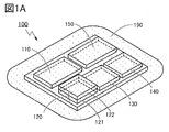
- FIG. 1A is a perspective view of the semiconductor device 100.
- 1B and 1C are diagrams illustrating a usage example of the semiconductor device 100.
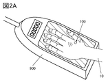
- 2A, 2B, 2C, 2D, and 2E are diagrams illustrating a usage example of the semiconductor device 100.
- FIG. 3 is a block diagram illustrating the configuration of the communication unit.
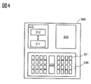
- FIG. 4 is a block diagram illustrating a configuration example of a semiconductor device.
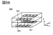
- 5A and 5B are diagrams illustrating a configuration example of a semiconductor device.
- 6A and 6B are diagrams illustrating a configuration example of a storage circuit.
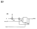
- FIG. 7 is a diagram illustrating a configuration example of an arithmetic circuit.
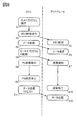
- FIG. 8 is a diagram illustrating an operation example of the semiconductor device.
- FIG. 1A is a perspective view of the semiconductor device 100.
- 1B and 1C are diagrams illustrating a usage example of the semiconductor device 100.
- 2A, 2B, 2C, 2D, and 2E are
- FIG. 9 is a diagram illustrating a configuration example of the CPU.
- 10A and 10B are diagrams illustrating a configuration example of a CPU.
- FIG. 11 is a diagram illustrating a configuration example of the CPU.
- FIG. 12 is a diagram illustrating a structural example of the semiconductor device.
- 13A and 13B are diagrams for explaining a structural example of a transistor.
- the position, size, range, etc. of each configuration shown in the drawings and the like may not represent the actual position, size, range, etc. in order to facilitate understanding of the invention. Therefore, the disclosed invention is not necessarily limited to the position, size, range, etc. disclosed in the drawings and the like.
- the resist mask or the like may be unintentionally reduced due to processing such as etching, but it may not be reflected in the figure for the sake of easy understanding.
- FIG. 1A is a perspective external view of a semiconductor device 100 that can be embedded in a living body.
- the semiconductor device 100 includes a communication unit 110, a calculation unit 120, a control unit 130, a storage unit 140, and a sensor unit 150. Further, the semiconductor device 100 is covered with a covering material 190.
- the communication unit 110 has a function of receiving a signal transmitted from an external device (not shown) by wireless communication and transmitting the signal to the external device. Further, the communication unit 110 has a function of receiving electric power supplied from an external device in a non-contact manner.
- a battery may be provided in the semiconductor device 100.
- the battery has a function of storing the electric power required for the operation of the semiconductor device 100 and a function of supplying the electric power necessary for the operation.
- a primary battery or a secondary battery can be used.
- a lithium ion secondary battery may be used.
- the calculation unit 120 has a calculation circuit 121 and a storage circuit 122.
- the arithmetic circuit 121 has a function of performing arithmetic processing using the information contained in the storage circuit 122. Further, the arithmetic circuit 121 has a function of performing arithmetic processing using the information contained in the storage circuit 122 and the information acquired by the sensor unit 150. Further, the arithmetic circuit 121 has a function of performing arithmetic processing using the information contained in the storage unit 140.
- the calculation result is stored in the storage unit 140.
- the storage unit 140 has a function of holding the identification information of the semiconductor device 100. Further, the storage unit 140 has a function of storing programs and parameters related to the operation of the semiconductor device 100.
- a RAM Random Access Memory
- ROM Read Only Memory
- the control unit 130 has a function of controlling the operations of the communication unit 110, the calculation unit 120, the storage unit 140, and the sensor unit 150.
- the control unit 130 has a function of converting an analog signal supplied from the sensor unit 150 or the like into a digital signal.
- the control unit 130 has a function of transmitting identification information and / or a calculation result to the external device according to a signal supplied from the external device via the communication unit 110.
- the sensor unit 150 a sensor capable of detecting various information can be used.
- the sensor unit 150 may have a function of detecting at least one of temperature, vibration, pressure, inclination, acceleration, oxygen concentration, chemical substance, and the like.
- the sensor unit 150 may have a function of converting an analog signal into a digital signal.
- the semiconductor device 100 is preferably covered with a covering material 190.
- a covering material 190 By using the dressing 190, it is possible to prevent an inflammatory reaction or an allergic reaction from occurring after implantation in a living body. Further, by covering the semiconductor device 100 with the covering material 190, it is possible to prevent damage to the living body such as blood vessels and nerve tissues adjacent to the implanted site.
- Materials used for the covering material 190 include biocompatible glass and polymer materials such as silicone resin and fluororesin.
- FIG. 1B and 1C are schematic views showing a state in which the semiconductor device 100 is embedded in the living body 10.
- FIG. 1B shows a state in which the semiconductor device 100 is embedded subcutaneously between the thumb and the index finger of the living body 10.
- FIG. 1C shows a state in which the semiconductor device 100 is embedded under the skin of the neck of the living body 10.
- the semiconductor device 100 embedded in the living body 10 can acquire biological information such as the body temperature and the heart rate of the living body 10. Further, by imparting identification information unique to the living body 10 to the semiconductor device 100, the semiconductor device 100 can be attached to a personal identification tag (for example, an individual number card (my number card), etc.), a driver's license, a health insurance card, a passport, and a cash. It can function as a card, credit card, etc.
- a personal identification tag for example, an individual number card (my number card), etc.
- a driver's license for example, a driver's license, a health insurance card, a passport, and a cash. It can function as a card, credit card, etc.
- the information of the living body 10 can be read out by superimposing the semiconductor device 100 embedded in the living body 10 on the external device 900.
- the external device 900 has a function of transmitting a signal to the semiconductor device 100 and a function of receiving a signal transmitted from the semiconductor device 100.
- the external device 900 functions as a reader / writer.
- the semiconductor device 100 can be embedded in various living bodies. For example, as shown in FIGS. 2B to 2E, it can be embedded in a living body 21, a living body 22, a living body 23, a living body 24, and the like. By using the semiconductor device 100, it is possible to prevent the theft of the living body 21 to 24, grasp the behavior, manage the health condition, and the like.
- FIG. 3 is a block diagram illustrating the configuration of the communication unit 110.
- the communication unit 110 includes an RF circuit 111 and an information processing circuit 117. Further, the RF circuit 111 includes a resonance circuit 112, a power supply circuit 113, a clock generation circuit 114, a demodulation circuit 115, and a modulation circuit 116.
- the resonance circuit 112 is connected to the power supply circuit 113, the clock generation circuit 114, the demodulation circuit 115, and the modulation circuit 116.
- the resonance circuit 112 has a function of converting an electromagnetic wave emitted from an external device into an AC signal.
- the signal includes information such as an operation command.
- the power supply circuit 113 has a function of generating electric power used for the operation of the semiconductor device 100 from the signal.
- the clock generation circuit 114 has a function of generating a synchronization signal necessary for the operation of the semiconductor device 100 from the signal.
- the demodulation circuit 115 has a function of extracting information such as an operation command from the signal.
- the information processing circuit 117 has a function of extracting an instruction from the information extracted from the demodulation circuit 115 and transmitting it to the control unit 130. Further, the information processing circuit 117 has a function of supplying the signal supplied from the control unit 130 to the modulation circuit 116.
- the modulation circuit 116 has a function of mixing the signal supplied from the control unit 130 with the carrier wave. Further, the resonance circuit 112 has a function of transmitting the signal mixed by the modulation circuit 116 to the outside.
- the semiconductor device 300 that can be used for the arithmetic unit 120 will be described.
- the arithmetic circuit 360 described later corresponds to the arithmetic circuit 121 of the arithmetic unit 120.
- the storage circuit 350 which will be described later, corresponds to the storage circuit 122 of the arithmetic unit 120.
- the semiconductor device 300 described in this embodiment is a semiconductor device having excellent calculation efficiency and capable of operating at extremely low power consumption.
- it is a semiconductor device that can function as a computer (Brain Functional Computer: also called BMC) that has the potential to imitate the functions of the human brain.
- BMC Brain Functional Computer
- FIG. 4 shows a block diagram illustrating the configuration of the semiconductor device 300.
- the semiconductor device 300 has a CPU 310, a bus 320, and an accelerator 330.
- the CPU 310 has a CPU core 311 and a backup circuit 312.
- the accelerator 330 has, in addition to the plurality of arithmetic blocks 331, a control unit 332 for controlling the input / output of data between the arithmetic blocks 331.
- the CPU 310 has functions for performing general-purpose processing such as execution of an operating system, control of data, execution of various operations, and execution of programs.
- the CPU 310 has a CPU core 311.
- the CPU core 311 corresponds to one or more CPU cores.
- the CPU 310 has a backup circuit 312 that can hold the data in the CPU core 311 even if the supply of the power supply voltage is stopped.
- the supply of the power supply voltage can be controlled by electrical disconnection from the power supply domain (power domain) by a power switch or the like.
- the power supply voltage may be referred to as a drive voltage.
- an OS memory having an OS transistor is suitable.
- the OS memory refers to a memory having a transistor (OS transistor) having an oxide semiconductor in a channel forming region, such as NOSRAM.
- NOSRAM registered trademark
- NOSRAM is an abbreviation for "Nonvolatile Oxide Semiconductor RAM”.
- the metal oxides applied to the OS transistor are Zn oxide, Zn-Sn oxide, Ga-Sn oxide, In-Ga oxide, In-Zn oxide, and In-M-Zn oxide (M is: Ti, Ga, Y, Zr, La, Ce, Nd, Sn or Hf) and the like.
- M is: Ti, Ga, Y, Zr, La, Ce, Nd, Sn or Hf
- oxides containing indium and zinc include aluminum, gallium, ittrium, copper, vanadium, beryllium, boron, silicon, titanium, iron, nickel, germanium, zirconium, molybdenum, lanthanum, cerium, neodymium, hafnium, tantalum, and tungsten. , One or more selected from magnesium and the like may be included.
- the metal oxide applied to the semiconductor layer is preferably a metal oxide having a crystal portion such as CAAC-OS, CAC-OS, and nc-OS.
- CAAC-OS is an abbreviation for c-axis-aligned crystalline oxide semiconductor ductor.
- CAC-OS is an abbreviation for Cloud-Aligned Composite oxide semiconductor ductor.
- nc-OS is an abbreviation for nanocrystalline oxide semiconductor ductor.
- the OS transistor has an extremely small leakage current, that is, a current flowing between the source and the drain in the off state.
- the NOSRAM can be used as a non-volatile memory by holding a charge corresponding to the data in the memory circuit using the characteristic that the leakage current is extremely small.
- NOSRAM can read the held data without destroying it (non-destructive reading), it is suitable for parallel processing of the product-sum operation of the neural network in which the data reading operation is repeated many times.
- the OS transistor Since the bandgap of the metal oxide that functions as an oxide semiconductor is 2.5 eV or more, the OS transistor has a minimum off current. As an example, voltage 3.5V between the source and the drain, at at room temperature (25 °C), 1 ⁇ less than 10 -20 A state current per channel width 1 [mu] m, less than 1 ⁇ 10 -22 A, or 1 ⁇ 10 It can be less than -24A. Therefore, in the OS memory, the amount of charge leaked from the holding node via the OS transistor is extremely small. Therefore, since the OS memory can function as a non-volatile memory circuit, power gating of the CPU 310 becomes possible.
- the backup circuit 312 configured by the OS transistor can be provided by stacking with the CPU core 311 which can be configured by a transistor (Si transistor) having silicon in the channel forming region. Since the area of the backup circuit 312 is smaller than the area of the CPU core 311, the backup circuit 312 can be arranged on the CPU core 311 without increasing the circuit area.
- the backup circuit 312 has a function of holding the register data of the CPU core 311.
- the backup circuit 312 is also referred to as a data holding circuit.
- the semiconductor layer including the channel forming region of the Si transistor may be a single crystal semiconductor or a polycrystalline semiconductor.
- the control unit 332 has a memory circuit such as an SRAM inside.
- the control unit 332 holds the output data obtained by the plurality of calculation blocks 331 in the memory circuit. Then, the output data held in the memory circuit is output to a plurality of semiconductor devices. With this configuration, it is possible to perform parallel calculation with an increased number of parallels using a plurality of semiconductor devices.
- the bus 320 electrically connects the CPU 310 and the accelerator 330. That is, the CPU 310 and the accelerator 330 can transmit data via the bus 320.
- the accelerator 330 described above executes a program (also referred to as a kernel or a kernel program) called from the host program.
- the accelerator 330 can perform, for example, parallel processing of matrix operations in graphic processing, parallel processing of product-sum operations of neural networks, parallel processing of floating-point operations in scientific and technological calculations, and the like.
- a configuration example of the arithmetic block 331 that performs arithmetic processing (parallel processing) of a plurality of data in parallel in the accelerator 330 will be described.
- the calculation block 331 has a plurality of calculation units 340 as shown in FIG. 5A.
- the arithmetic unit 340 has a storage circuit 350 and an arithmetic circuit 360.
- the storage circuit 350 and the arithmetic circuit 360 are provided in different layers in a direction substantially perpendicular to the XY plane in the figure (Z direction in FIG. 5A). That is, the storage circuit 350 and the arithmetic circuit 360 are provided in a stacked manner.
- the term "approximately vertical” means a state in which the particles are arranged at an angle of 85 degrees or more and 95 degrees or less.
- the X direction, the Y direction, and the Z direction shown in FIG. 5B and the like are directions orthogonal to or intersecting each other. Further, the X direction and the Y direction are parallel or substantially parallel to the substrate surface, and the Z direction is perpendicular or substantially perpendicular to the substrate surface.
- the storage circuit 350 has a plurality of memory cells. Writing and reading of data to the memory cell is controlled by the drive circuit 341 and the drive circuit 342.
- the drive circuit 341 and the drive circuit 342 are also referred to as a data control circuit.
- the information (data) stored in the memory cell in the storage circuit 350 is data (weight data) corresponding to the weight parameter used in the product-sum operation of the neural network.
- data weight data
- the weight data may be analog data.
- the storage circuit 350 is connected to the arithmetic circuit 360 via wiring.
- the memory cell included in the storage circuit 350 has an OS transistor.
- the wiring connecting the storage circuit 350 and the calculation circuit 360 is a wiring for transmitting weight data from the storage circuit 350 to the calculation circuit 360.
- the wiring can be configured to extend in the z direction as shown by the arrow 351 in FIG. 5B.
- the arithmetic circuit 360 has a function of executing arithmetic processing such as a product-sum operation.
- the input and output of the data of the arithmetic circuit 360 are controlled by the control circuit 343 and the control circuit 344.
- the control circuit 343 and the control circuit 344 are also referred to as a data input / output circuit.
- the calculation circuit 360 performs a product-sum calculation of the input data input from the control circuit 343 and the weight data given by the storage circuit 350.
- the input data may be biometric information detected by the sensor unit 150.
- the obtained product-sum operation data is output to the control circuit 344.
- the input data and the weight data may be analog data or digital data.
- the input data and the weight data are preferably digital data. Digital data is less susceptible to noise. Therefore, digital data is suitable for performing arithmetic processing that requires highly accurate arithmetic results.
- the arithmetic circuit 360 By configuring the arithmetic circuit 360 with a Si transistor, it can be provided so as to be laminated with an OS transistor. That is, the storage circuit 350 composed of the OS transistor can be provided so as to be laminated with the arithmetic circuit 360 that can be configured by the Si transistor. Therefore, the area where the storage circuit 350 can be arranged can be increased without increasing the circuit area. By setting the area where the storage circuit 350 is provided on the substrate on which the arithmetic circuit 360 is provided, the arithmetic processing in the accelerator 330 can be performed as compared with the case where the storage circuit 350 and the arithmetic circuit 360 are arranged on the same layer. The required storage capacity can be increased. By increasing the storage capacity, it is possible to reduce the number of times data used for arithmetic processing is transferred from the external storage device to the semiconductor device, so that power consumption can be reduced.
- ⁇ Memory circuit> A configuration example of NOSRAM, which is a memory cell included in the storage circuit 350, will be described.
- writing word lines WWL_1 to WWL_M, reading word lines RWL_1 to RWL_M, and writing bit lines WBL_1 are arranged side by side in the matrix direction of M rows and N columns (M and N are natural numbers of 2 or more).
- WBL_N and wiring LBL_1 to LBL_N are illustrated.
- a memory cell 352 connected to each word line and bit line is illustrated.
- FIG. 6B is a diagram illustrating an example circuit configuration applicable to the memory cell 352.
- the memory cell 352 has a transistor 353, a transistor 354, a transistor 355, and a capacitive element 356 (also referred to as a capacitor).
- One of the source and drain of the transistor 353 is connected to the writing bit line WBL.
- the gate of the transistor 353 is connected to the writing word line WWL.
- the other of the source or drain of the transistor 353 is connected to one electrode of the capacitive element 356 and the gate of the transistor 354.
- One of the source or drain of the transistor 354 and the other electrode of the capacitive element 356 are connected to a wire that provides a fixed potential, eg, a ground potential.
- the other of the source or drain of the transistor 354 is connected to one of the source or drain of the transistor 355.
- the gate of the transistor 355 is connected to the read word line RWL.
- the other of the source or drain of the transistor 355 is connected to the wiring LBL.
- the wiring LBL is connected to the arithmetic circuit 360 (not shown) via wiring provided so as to extend in a direction substantially perpendicular to the surface of the substrate on which the Si transistor of the arithmetic circuit 360 is provided.
- the circuit configuration of the memory cell 352 shown in FIG. 6B corresponds to the NOSRAM of the 3-transistor type (3T) gain cell.
- the transistor 353 to the transistor 355 are OS transistors.
- the OS transistor has an extremely small leakage current, that is, a current flowing between the source and the drain in the off state.
- the NOSRAM can be used as a non-volatile memory by holding a charge corresponding to the data in the memory circuit using the characteristic that the leakage current is extremely small.
- FIG. 7 shows a specific configuration example of the arithmetic circuit 360.
- FIG. 7 illustrates a configuration example of an arithmetic circuit 360 capable of performing a product-sum operation of weight data W and input data A.
- the multiplication circuit 361, the addition circuit 362, and the register 363 are illustrated.
- the data multiplied by the multiplication circuit 361 is input to the addition circuit 362.
- the output of the addition circuit 362 is held in the register 363, and the product-sum operation is performed by adding the data to be multiplied by the multiplication circuit 361 and the addition circuit 362.
- the register 363 is controlled by the clock signal CLK and the reset signal reset_B. With this configuration, a data MAC corresponding to the product-sum operation of the weight data W and the input data A can be obtained.
- FIG. 8 is a diagram illustrating an example of an operation when a part of the operation of the program executed by the CPU is executed by the accelerator.
- the host program is executed on the CPU (host program execution; step S1).
- the CPU transmits weight data, which is input data, from the main memory or an external storage device to the storage circuit (memory) (data transmission; step S4).
- the storage circuit (memory) receives the weight data and stores the weight data in the area secured in step S2 (data reception; step S5).
- step S6 When the CPU confirms the instruction to start the kernel program (starting the kernel program; step S6), the accelerator starts executing the kernel program (starting calculation; step S7).
- the CPU may be switched from the state of performing arithmetic to the PG (power gating) state (PG state transition; step S8). In that case, immediately before the accelerator finishes executing the kernel program, the CPU is switched from the PG state to the state in which the calculation is performed (PG state stop step S9).
- PG state transition a state in which the calculation is performed.
- step S10 When the accelerator finishes executing the kernel program, the output data is stored in the storage unit that holds the calculation result in the accelerator (completion of calculation; step S10).
- step S11 After the execution of the kernel program is completed, when the CPU confirms the instruction to transmit the output data stored in the storage unit to the main memory or the external storage device (data transmission request; step S11), the above output data is output. It is transmitted to the main memory or the external storage device and stored in the main memory or the external storage device (data transmission; step S12).
- the semiconductor device of one aspect of the present invention may have a non-Von Neumann architecture.
- the non-von Neumann architecture can perform arithmetic processing with extremely low power consumption as compared with the von Neumann architecture in which the power consumption increases as the processing speed increases.
- FIG. 9 shows a configuration example of the CPU 310.
- the CPU 310 includes a CPU core (CPU Core) 311 and an L1 (level 1) cache memory device (L1 cache) 371, an L2 cache memory device (L2 cache) 372, a bus interface unit (Bus I / F) 373, and a power switch 315 to. It has 317, a level shifter (LS) 318.
- the CPU core 311 has a flip-flop 314.
- the CPU core 311 and the L1 cache memory device 371 and the L2 cache memory device 372 are connected to each other by the bus interface unit 373.
- the PMU 313 generates a clock signal GCLK1 and various PG (power gating) control signals (PG control signals) in response to signals such as interrupt signals (Interrupts) input from the outside and signals SLEEP1 issued by the CPU 310.
- the clock signals GCLK1 and PG control signals are input to the CPU 310.
- the PG control signal controls the power switches 315 to 317 and the flip-flop 314.
- the power switches 315 and 316 control the supply of the voltages VDDD and VDD1 to the virtual power supply line V_ achievement (hereinafter referred to as V_ VDD line), respectively.
- the power switch 317 controls the supply of the voltage VDDH to the level shifter (LS) 318.
- the voltage VSSS is input to the CPU 310 and the PMU 313 without going through the power switch.
- the voltage VDDD is input to the PMU 313 without going through the power switch.
- the voltages VDDD and VDD1 are drive voltages for CMOS circuits.
- the voltage VDD1 is lower than the voltage VDDD and is the drive voltage in the sleep state.
- the voltage VDDH is the drive voltage for the OS transistor and is higher than the voltage VDDD.
- Each of the L1 cache memory device 371, the L2 cache memory device 372, and the bus interface unit 373 has at least one power gating power domain.
- a power domain capable of power gating is provided with one or more power switches. These power switches are controlled by PG control signals.
- the flip-flop 314 is used as a register.
- the flip-flop 314 is provided with a backup circuit. Hereinafter, the flip-flop 314 will be described.
- FIG. 10A shows an example of a circuit configuration of a flip-flop 314 (Flip-flop).
- the flip-flop 314 has a scan flip-flop (Scan Flip-flop) 319 and a backup circuit (Backup Circuit) 312.
- the scan flip-flop 319 has nodes D1, Q1, SD, SE, RT, CK, and a clock buffer circuit 319A.
- Node D1 is a data (data) input node
- node Q1 is a data output node
- node SD is a scan test data input node.
- the node SE is an input node of the signal SCE.
- the node CK is an input node for the clock signal GCLK1.
- the clock signal GCLK1 is input to the clock buffer circuit 319A.
- the analog switch of the scan flip-flop 319 is connected to the nodes CK1 and CKB1 of the clock buffer circuit 319A.
- the node RT is an input node for a reset signal.
- the signal SCE is a scan enable signal and is generated by the PMU 313.
- PMU313 generates signals BK and RC.
- the level shifter 318 level-shifts the signals BK and RC to generate the signals BKH and RCH.
- the signal BK is a backup signal and the signal RC is a recovery signal.
- the circuit configuration of the scan flip-flop 319 is not limited to FIG. 10A. Flip-flops provided in standard circuit libraries can be applied.
- the backup circuit 312 includes nodes SD_IN, SN11, transistors M11 to M13, and a capacitive element C11.
- the node SD_IN is an input node for scan test data and is connected to node Q1 of the scan flip-flop 319.
- the node SN11 is a holding node of the backup circuit 312.
- the capacitance element C11 is a holding capacitance for holding the voltage of the node SN11.
- the transistor M11 controls the conduction state between the node Q1 and the node SN11.
- the transistor M12 controls the conduction state between the node SN11 and the node SD.
- the transistor M13 controls the conduction state between the node SD_IN and the node SD.
- the on / off of the transistors M11 and M13 is controlled by the signal BKH, and the on / off of the transistors M12 is controlled by the signal RH.
- the transistors M11 to M13 are OS transistors like the transistors 353 to 355 included in the memory cell 352 described above.
- the transistors M11 to M13 show a configuration having a back gate.
- the back gates of the transistors M11 to M13 are connected to a power supply line that supplies the voltage VBG1.
- the backup circuit 312 has a non-volatile characteristic because the off current is extremely small, the voltage drop of the node SN11 can be suppressed, and almost no power is consumed to hold the data. Since the data is rewritten by charging / discharging the capacitive element C11, the backup circuit 312 is not limited in the number of rewritings in principle, and the data can be written and read with a small amount of power.
- the backup circuit 312 can be laminated on the scan flip-flop 319 composed of the silicon CMOS circuit.
- the backup circuit 312 Since the backup circuit 312 has a very small number of elements as compared with the scan flip-flop 319, it is not necessary to change the circuit configuration and layout of the scan flip-flop 319 in order to stack the backup circuits 312. That is, the backup circuit 312 is a very versatile backup circuit. Further, since the backup circuit 312 can be provided in the region where the scan flip-flop 319 is formed, it is possible to make the increase in the occupied area of the flip-flop 314 zero even if the backup circuit 312 is incorporated. Therefore, by providing the backup circuit 312 on the flip-flop 314, power gating of the CPU core 311 becomes possible. Since the power required for power gating is small, it is possible to power gate the CPU core 311 with high efficiency.
- the backup circuit 312 By providing the backup circuit 312, the parasitic capacitance due to the transistor M11 is added to the node Q1, but since it is smaller than the parasitic capacitance due to the logic circuit connected to the node Q1, the scan flip-flop 319 can be operated. There is no effect. That is, even if the backup circuit 312 is provided, the performance of the flip-flop 314 is not substantially deteriorated.
- the low power consumption state of the CPU core 31 for example, a clock gating state, a power gating state, and a hibernation state can be set.
- the PMU 313 selects the low power consumption mode of the CPU core 311 based on the interrupt signal, the signal SLEEP1, and the like. For example, when shifting from the normal operating state to the clock gating state, the PMU 313 stops the generation of the clock signal GCLK1.
- the PMU 313 when transitioning from a normal operating state to a hibernate state, the PMU 313 performs voltage and / or frequency scaling. For example, when performing voltage scaling, the PMU 313 turns off the power switch 315 and turns on the power switch 316 in order to input the voltage VDD1 to the CPU core 311.
- the voltage VDD1 is a voltage that does not cause the data of the scan flip-flop 319 to be lost.
- frequency scaling is performed, the PMU 313 lowers the frequency of the clock signal GCLK1.
- FIG. 11 shows an example of the power gating sequence of the CPU core 311.
- t1 to t7 represent the time.
- the signals PSE0 to PSE2 are control signals of the power switches 315 to 317 and are generated by the PMU 313.
- the power switch 315 is on / off. The same applies to the signals PSE1 and PSE2.
- the PMU 313 stops the clock signal GCLK1 and sets the signals PSE2 and BK to “H”.
- the level shifter 318 becomes active and outputs the “H” signal BKH to the backup circuit 312.
- the transistor M11 of the backup circuit 312 is turned on, and the data of the node Q1 of the scan flip-flop 319 is written to the node SN11 of the backup circuit 312. If the node Q1 of the scan flip-flop 319 is "L”, the node SN11 remains “L”, and if the node Q1 is "H”, the node SN11 becomes "H”.
- the PMU 313 sets the signals PSE2 and BK to “L” at time t2, and sets the signal PSE0 to “L” at time t3. At time t3, the state of the CPU core 311 shifts to the power gating state.
- the signal PSE0 may be turned off at the timing of lowering.
- the PMU 313 sets the signal PSE0 to “H” to shift from the power gating state to the recovery state.
- the PMU313 sets the signals PSE2, RC, and SCE to "H” in a state where the charging of the V_ VDD line is started and the voltage of the V_ldap line becomes VDDD (time t5).
- the transistor M12 is turned on and the charge of the capacitive element C11 is distributed to the node SN 11 and the node SD. If the node SN11 is "H”, the voltage of the node SD rises. Since the node SE is “H”, the data of the node SD is written to the input side latch circuit of the scan flip-flop 319. When the clock signal GCLK1 is input to the node CK at time t6, the data of the input side latch circuit is written to the node Q1. That is, the data of the node SN11 is written to the node Q1.
- the PMU 313 sets the signals PSE2, SCE, and RC to “L”, and the recovery operation ends.
- the backup circuit 312 using an OS transistor is very suitable for normal-off computing because it has low dynamic and static low power consumption.
- the CPU 310 including the CPU core 311 having the backup circuit 312 using the OS transistor can be referred to as a Noff CPU (registered trademark).
- the Noff CPU has a non-volatile memory and can stop the power supply when the operation is not required. Even if the flip-flop 314 is mounted, it is possible to hardly cause a decrease in performance of the CPU core 311 and an increase in dynamic power.
- the CPU core 311 may have a plurality of power domains capable of power gating.
- the plurality of power domains are provided with one or more power switches for controlling the voltage input.
- the CPU core 311 may have one or a plurality of power domains in which power gating is not performed.
- a power gating control circuit for controlling the flip-flop 314 and the power switches 315 to 317 may be provided in the power domain where power gating is not performed.
- the application of the flip-flop 314 is not limited to the CPU 310.
- the flip-flop 314 can be applied to a register provided in a power domain capable of power gating.
- Embodiment 2 In this embodiment, a configuration example of a transistor applicable to the semiconductor device described in the above embodiment will be described. As an example, a configuration in which transistors having different electrical characteristics are laminated and provided will be described. With this configuration, the degree of freedom in designing the semiconductor device can be increased. Further, by stacking transistors having different electrical characteristics, the degree of integration of the semiconductor device can be increased.
- FIG. 12 shows a part of the cross-sectional structure of the semiconductor device.
- the semiconductor device shown in FIG. 12 includes a transistor 550, a transistor 500, and a capacitive element 600.
- 13A is a cross-sectional view of the transistor 500 in the channel length direction
- FIG. 13B is a cross-sectional view of the transistor 500 in the channel width direction.
- the transistor 500 corresponds to an OS transistor included in the storage circuit 350 shown in the above embodiment, that is, a transistor having an oxide semiconductor in a channel forming region.
- the transistor 550 corresponds to a Si transistor included in the arithmetic circuit 360 shown in the above embodiment, that is, a transistor having silicon in the channel forming region.
- the capacitive element 600 corresponds to the capacitive element of the storage circuit 350.
- the transistor 500 is an OS transistor.
- the OS transistor has an extremely small off current. Therefore, it is possible to hold the data voltage or charge written to the storage node via the transistor 500 for a long period of time. That is, the frequency of refreshing operations of the storage node is reduced, or the refreshing operation is not required, so that the power consumption of the semiconductor device can be reduced.
- the transistor 500 is provided above the transistor 550, and the capacitive element 600 is provided above the transistor 550 and the transistor 500.
- the transistor 550 is provided on the substrate 411.
- the substrate 411 is, for example, a p-type silicon substrate.
- the substrate 411 may be an n-type silicon substrate.
- the oxide layer 414 is preferably an insulating layer (also referred to as a BOX layer) formed in a substrate 411 by embedded oxidation (Blured oxide), for example, silicon oxide.
- the transistor 550 is provided on a single crystal silicon, a so-called SOI (Silicon On Insulator) substrate, which is provided on the substrate 411 via an oxide layer 414. Therefore, in the present embodiment and the like, the transistor 550 is a Si transistor.
- the substrate 411 in the SOI substrate is provided with an insulator 413 that functions as an element separation layer.
- the substrate 411 also has a well region 412.
- the well region 412 is a region to which n-type or p-type conductivity is imparted depending on the conductive type of the transistor 550.
- the single crystal silicon in the SOI substrate is provided with a semiconductor region 415, a low resistance region 416a that functions as a source region or a drain region, and a low resistance region 416b. Further, a low resistance region 416c is provided on the well region 412.
- the transistor 550 can be provided so as to be superimposed on the well region 412 to which the impurity element that imparts conductivity is added.
- the well region 412 can function as a bottom gate electrode of the transistor 550 by independently changing the potential via the low resistance region 416c. Therefore, the threshold voltage of the transistor 550 can be controlled.
- the threshold voltage of the transistor 550 can be made larger and the off-current can be reduced. Therefore, by applying a negative potential to the well region 412, the drain current when the potential applied to the gate electrode of the Si transistor is 0V can be reduced. As a result, the power consumption of the semiconductor device having the transistor 550 can be reduced, and the calculation efficiency can be improved.
- the transistor 550 is preferably of a so-called Fin type in which the upper surface of the semiconductor layer and the side surface in the channel width direction are covered with the conductor 418 via the insulator 417.
- the on characteristic of the transistor 550 can be improved by increasing the effective channel width. Further, since the contribution of the electric field of the gate electrode can be increased, the off characteristic of the transistor 550 can be improved.
- the transistor 550 may be either a p-channel type transistor or an n-channel type transistor.
- the conductor 418 may function as a first gate (also referred to as a top gate) electrode. Further, the well region 412 may function as a second gate (also referred to as a bottom gate) electrode. In that case, the potential applied to the well region 412 can be controlled via the low resistance region 416c.
- the low resistance region 416a that becomes the region where the channel of the semiconductor region 415 is formed, the region in the vicinity thereof, the source region, or the drain region, and the low resistance region 416b and the well region 412 connected to the electrodes that control the potential.
- the region 416c or the like preferably contains a semiconductor such as a silicon-based semiconductor, and preferably contains single crystal silicon. Alternatively, it may be formed of a material having Ge (germanium), SiGe (silicon germanium), GaAs (gallium arsenide), GaAlAs (gallium aluminum arsenide), or the like. A configuration using silicon in which the effective mass is controlled by applying stress to the crystal lattice and changing the lattice spacing may be used.
- the transistor 550 may be a HEMT (High Electron Mobility Transistor) by using GaAs, GaAlAs, or the like.
- the semiconductor material applied to the semiconductor region 415, the well region 412, the low resistance region 416a, the low resistance region 416b, and the low resistance region 416c are elements that impart n-type conductivity such as arsenic and phosphorus, or boron. It contains elements that impart p-type conductivity such as.
- the conductor 418 that functions as a gate electrode is a semiconductor material such as silicon, a metal material, or an alloy containing an element that imparts n-type conductivity such as arsenic or phosphorus, or an element that imparts p-type conductivity such as boron.
- a conductive material such as a material or a metal oxide material can be used.
- a silicide such as nickel silicide may be used as the conductor 418.
- the threshold voltage of the transistor can be adjusted by selecting the material of the conductor. Specifically, it is preferable to use a material such as titanium nitride or tantalum nitride for the conductor. Further, in order to achieve both conductivity and embedding property, it is preferable to use a metal material such as tungsten or aluminum as a laminate for the conductor, and it is particularly preferable to use tungsten in terms of heat resistance.
- the low resistance region 416a, the low resistance region 416b, and the low resistance region 416c may be configured by laminating another conductor, for example, a silicide such as nickel silicide. With this configuration, the conductivity of the region that functions as an electrode can be enhanced.
- the side surface of the conductor 418 that functions as the gate electrode and the side surface of the insulator 417 that functions as the gate insulating film may be provided with an insulator that functions as a side wall spacer (also referred to as a side wall insulating layer). good. With this configuration, it is possible to prevent the conductor 418 and the low resistance region 416a and the low resistance region 416b from being in a conductive state.
- An insulator 420, an insulator 422, an insulator 424, and an insulator 426 are laminated in this order so as to cover the transistor 550.
- the insulator 420, the insulator 422, the insulator 424, and the insulator 426 for example, silicon oxide, silicon oxide, silicon nitride, silicon nitride, aluminum oxide, aluminum oxide, aluminum nitride, aluminum nitride, etc. are used. Just do it.
- silicon oxynitride refers to a material having a higher oxygen content than nitrogen as its composition
- silicon nitride as its composition refers to a material having a higher nitrogen content than oxygen as its composition. Is shown.
- aluminum nitride refers to a material whose composition has a higher oxygen content than nitrogen
- aluminum nitride refers to a material whose composition has a higher nitrogen content than oxygen. Is shown.
- the insulator 422 may have a function as a flattening film for flattening a step generated by a transistor 550 or the like provided below the insulator 422.
- the upper surface of the insulator 422 may be flattened by a flattening treatment using a chemical mechanical polishing (CMP) method or the like in order to improve the flatness.
- CMP chemical mechanical polishing
- the insulator 424 it is preferable to use a film having a barrier property so that hydrogen and impurities do not diffuse in the region where the transistor 500 is provided from the substrate 411 or the transistor 550.
- a film having a barrier property against hydrogen for example, silicon nitride formed by the CVD method can be used.
- hydrogen may diffuse into a semiconductor element having an oxide semiconductor such as a transistor 500, which may deteriorate the characteristics of the semiconductor element. Therefore, it is preferable to use a film that suppresses the diffusion of hydrogen between the transistor 500 and the transistor 550.
- the membrane that suppresses the diffusion of hydrogen is a membrane that desorbs a small amount of hydrogen.
- the amount of hydrogen desorbed can be analyzed using, for example, a heated desorption gas analysis method (TDS).
- TDS heated desorption gas analysis method
- the amount of hydrogen desorbed from the insulator 424 is the amount desorbed in terms of hydrogen atoms in the range of 50 ° C. to 500 ° C. in the surface temperature of the film in TDS analysis, which is converted per area of the insulator 424. It may be 10 ⁇ 10 15 atoms / cm 2 or less, preferably 5 ⁇ 10 15 atoms / cm 2 or less.
- the insulator 426 preferably has a lower dielectric constant than the insulator 424.
- the relative permittivity of the insulator 426 is preferably less than 4, more preferably less than 3.
- the relative permittivity of the insulator 426 is preferably 0.7 times or less, more preferably 0.6 times or less the relative permittivity of the insulator 424.
- the insulator 420, the insulator 422, the insulator 424, and the insulator 426 are embedded with a capacitive element 600, a conductor 428 connected to the transistor 500, a conductor 430, and the like.
- the conductor 428 and the conductor 430 have a function as a plug or wiring.
- the conductor having a function as a plug or a wiring may collectively give the same reference numeral to a plurality of configurations.
- the wiring and the plug connected to the wiring may be integrated. That is, a part of the conductor may function as a wiring, and a part of the conductor may function as a plug.
- each plug and wiring As the material of each plug and wiring (conductor 428, conductor 430, etc.), a conductive material such as a metal material, an alloy material, a metal nitride material, or a metal oxide material is used as a single layer or laminated. be able to. It is preferable to use a refractory material such as tungsten or molybdenum that has both heat resistance and conductivity, and it is preferable to use tungsten. Alternatively, it is preferably formed of a low resistance conductive material such as aluminum or copper. Wiring resistance can be reduced by using a low resistance conductive material.
- a wiring layer may be provided on the insulator 426 and the conductor 430.
- the insulator 450, the insulator 452, and the insulator 454 are laminated in this order.
- a conductor 456 is formed on the insulator 450, the insulator 452, and the insulator 454.
- the conductor 456 has a function as a plug or wiring for connecting to the transistor 550.
- the conductor 456 can be provided by using the same materials as the conductor 428 and the conductor 430.
- the insulator 450 it is preferable to use an insulator having a barrier property against hydrogen, similarly to the insulator 424.
- the conductor 456 preferably contains a conductor having a barrier property against hydrogen.
- a conductor having a barrier property against hydrogen is formed in the opening of the insulator 450 having a barrier property against hydrogen.
- the conductor having a barrier property against hydrogen for example, tantalum nitride or the like may be used. Further, by laminating tantalum nitride and tungsten having high conductivity, it is possible to suppress the diffusion of hydrogen from the transistor 550 while maintaining the conductivity as wiring. In this case, it is preferable that the tantalum nitride layer having a barrier property against hydrogen is in contact with the insulator 450 having a barrier property against hydrogen.
- a wiring layer may be provided on the insulator 454 and the conductor 456.
- the insulator 460, the insulator 462, and the insulator 464 are laminated in this order.
- a conductor 466 is formed on the insulator 460, the insulator 462, and the insulator 464.
- the conductor 466 has a function as a plug or wiring.
- the conductor 466 can be provided by using the same materials as the conductor 428 and the conductor 430.
- the insulator 460 it is preferable to use an insulator having a barrier property against hydrogen, similarly to the insulator 424.
- the conductor 466 preferably contains a conductor having a barrier property against hydrogen.
- a conductor having a barrier property against hydrogen is formed in the opening of the insulator 460 having a barrier property against hydrogen.
- a wiring layer may be provided on the insulator 464 and the conductor 466.
- the insulator 470, the insulator 472, and the insulator 474 are laminated in this order.
- a conductor 476 is formed on the insulator 470, the insulator 472, and the insulator 474.
- the conductor 476 has a function as a plug or wiring.
- the conductor 476 can be provided by using the same materials as the conductor 428 and the conductor 430.
- the insulator 470 it is preferable to use an insulator having a barrier property against hydrogen, similarly to the insulator 424.
- the conductor 476 preferably contains a conductor having a barrier property against hydrogen.
- a conductor having a barrier property against hydrogen is formed in the opening of the insulator 470 having a barrier property against hydrogen.
- a wiring layer may be provided on the insulator 474 and the conductor 476.
- the insulator 480, the insulator 482, and the insulator 484 are laminated in this order.
- a conductor 486 is formed on the insulator 480, the insulator 482, and the insulator 484.
- the conductor 486 has a function as a plug or wiring.
- the conductor 486 can be provided by using the same materials as the conductor 428 and the conductor 430.
- the insulator 480 it is preferable to use an insulator having a barrier property against hydrogen, similarly to the insulator 424.
- the conductor 486 preferably contains a conductor having a barrier property against hydrogen.
- a conductor having a barrier property against hydrogen is formed in the opening of the insulator 480 having a barrier property against hydrogen.
- the wiring layer including the conductor 456, the wiring layer including the conductor 466, the wiring layer including the conductor 476, and the wiring layer including the conductor 486 have been described, but the semiconductor device according to the present embodiment has been described. It is not limited to this.
- the number of wiring layers similar to the wiring layer including the conductor 456 may be three or less, or the number of wiring layers similar to the wiring layer including the conductor 456 may be five or more.
- An insulator 510, an insulator 512, an insulator 514, and an insulator 516 are laminated on the insulator 484 in this order.
- any of the insulator 510, the insulator 512, the insulator 514, and the insulator 516 it is preferable to use a substance having a barrier property against oxygen and hydrogen.
- the insulator 510 and the insulator 514 it is preferable to use a film having a barrier property against hydrogen and impurities in the region where the transistor 500 is provided, for example, from the region where the substrate 411 or the transistor 550 is provided. Therefore, the same material as the insulator 424 can be used.
- silicon nitride formed by the CVD method can be used as an example of a film having a barrier property against hydrogen.
- hydrogen may diffuse into a semiconductor element having an oxide semiconductor such as a transistor 500, which may deteriorate the characteristics of the semiconductor element. Therefore, it is preferable to use a film that suppresses the diffusion of hydrogen between the transistor 500 and the transistor 550.
- the film having a barrier property against hydrogen for example, it is preferable to use metal oxides such as aluminum oxide, hafnium oxide, and tantalum oxide for the insulator 510 and the insulator 514.
- metal oxides such as aluminum oxide, hafnium oxide, and tantalum oxide for the insulator 510 and the insulator 514.
- aluminum oxide has a high blocking effect that does not allow the membrane to permeate both oxygen and impurities such as hydrogen and water that cause fluctuations in the electrical characteristics of the transistor. Therefore, aluminum oxide can prevent impurities such as hydrogen and moisture from being mixed into the transistor 500 during and after the manufacturing process of the transistor. In addition, it is possible to suppress the release of oxygen from the oxides constituting the transistor 500. Therefore, it is suitable for use as a protective film for the transistor 500.
- the same material as that of the insulator 420 can be used for the insulator 512 and the insulator 516. Further, by applying a material having a relatively low dielectric constant to these insulators, it is possible to reduce the parasitic capacitance generated between the wirings.
- a silicon oxide film, a silicon nitride film, or the like can be used as the insulator 512 and the insulator 516.
- a conductor 518, a conductor constituting the transistor 500 (for example, a conductor 503) and the like are embedded in the insulator 510, the insulator 512, the insulator 514, and the insulator 516.
- the conductor 518 has a function as a plug or wiring for connecting to the capacitive element 600 or the transistor 550.
- the conductor 518 can be provided by using the same material as the conductor 428 and the conductor 430.
- the conductor 518 in the region in contact with the insulator 510 and the insulator 514 is preferably a conductor having a barrier property against oxygen, hydrogen, and water.
- the transistor 550 and the transistor 500 can be separated by a layer having a barrier property against oxygen, hydrogen, and water, and the diffusion of hydrogen from the transistor 550 to the transistor 500 can be suppressed.
- a transistor 500 is provided above the insulator 516.
- the transistor 500 has a conductor 503 arranged so as to be embedded in the insulator 514 and the insulator 516, and an insulator 522 arranged on the insulator 516 and the insulator 503. And an insulator 524 arranged on the insulator 522, an oxide 530a arranged on the insulator 524, an oxide 530b arranged on the oxide 530a, and each other on the oxide 530b. Insulator 580 and an opening which are arranged on the conductor 542a and the conductor 542b and which are arranged apart from each other and have an opening formed by superimposing between the conductor 542a and the conductor 542b. It has an insulator 545 arranged on the bottom surface and side surfaces of the insulator 545, and a conductor 560 arranged on the forming surface of the insulator 545.
- the insulator 544 is arranged between the oxide 530a, the oxide 530b, the conductor 542a, and the conductor 542b, and the insulator 580.
- the conductor 560 includes a conductor 560a provided inside the insulator 545 and a conductor 560b provided so as to be embedded inside the conductor 560a. It is preferable to have.
- the insulator 574 is arranged on the insulator 580, the conductor 560, and the insulator 545.
- oxide 530a and the oxide 530b may be collectively referred to as an oxide 530.
- the transistor 500 shows a configuration in which two layers of oxide 530a and oxide 530b are laminated in a region where a channel is formed and in the vicinity thereof, but the present invention is not limited to this.
- a single layer of the oxide 530b or a laminated structure of three or more layers may be provided.
- the conductor 560 is shown as a laminated structure of two layers, but the present invention is not limited to this.
- the conductor 560 may have a single-layer structure or a laminated structure of three or more layers.
- the transistor 500 shown in FIGS. 12, 13A, and 13B is an example, and the transistor 500 is not limited to the configuration thereof, and an appropriate transistor may be used depending on the circuit configuration, driving method, and the like.
- the conductor 560 functions as a gate electrode of the transistor, and the conductor 542a and the conductor 542b function as a source electrode or a drain electrode, respectively.
- the conductor 560 is formed so as to be embedded in the opening of the insulator 580 and the region sandwiched between the conductor 542a and the conductor 542b.
- the arrangement of the conductor 560, the conductor 542a and the conductor 542b is self-aligned with respect to the opening of the insulator 580. That is, in the transistor 500, the gate electrode can be arranged in a self-aligned manner between the source electrode and the drain electrode. Therefore, since the conductor 560 can be formed without providing the alignment margin, the occupied area of the transistor 500 can be reduced. As a result, the semiconductor device can be miniaturized and highly integrated.
- the conductor 560 is formed in a region between the conductor 542a and the conductor 542b in a self-aligned manner, the conductor 560 does not have a region overlapping with the conductor 542a or the conductor 542b. This makes it possible to reduce the parasitic capacitance formed between the conductor 560 and the conductors 542a and 542b. Therefore, the switching speed of the transistor 500 can be improved and high frequency characteristics can be provided.
- the conductor 560 may function as a first gate (also referred to as a top gate) electrode. Further, the conductor 503 may function as a second gate (also referred to as a bottom gate) electrode.
- the threshold voltage of the transistor 500 can be controlled by changing the potential applied to the conductor 503 independently of the potential applied to the conductor 560 without interlocking with the potential applied to the conductor 560. In particular, by applying a negative potential to the conductor 503, it is possible to increase the threshold voltage of the transistor 500 and reduce the off-current. Therefore, when a negative potential is applied to the conductor 503, the drain current when the potential applied to the conductor 560 is 0 V can be made smaller than when it is not applied.
- the conductor 503 is arranged so as to overlap the oxide 530 and the conductor 560. As a result, when a potential is applied to the conductor 560 and the conductor 503, the electric field generated from the conductor 560 and the electric field generated from the conductor 503 are connected to cover the channel forming region formed in the oxide 530. Can be done.
- the configuration of a transistor that electrically surrounds a channel forming region by an electric field of a pair of gate electrodes is referred to as a curved channel (S-channel) configuration.
- S-channel configuration disclosed in the present specification and the like is different from the Fin type configuration and the planar type configuration.
- the conductor 503 has the same structure as the conductor 518, and the conductor 503a is formed in contact with the inner walls of the openings of the insulator 514 and the insulator 516, and the conductor 503b is further formed inside.
- the transistor 500 shows a configuration in which the conductor 503a and the conductor 503b are laminated, the present invention is not limited to this.
- the conductor 503 may be provided as a single layer or a laminated structure having three or more layers.
- the conductor 503a it is preferable to use a conductive material having a function of suppressing the diffusion of impurities such as hydrogen atoms, hydrogen molecules, water molecules, and copper atoms (the above impurities are difficult to permeate).
- a conductive material having a function of suppressing the diffusion of oxygen for example, at least one such as an oxygen atom and an oxygen molecule
- the function of suppressing the diffusion of impurities or oxygen is a function of suppressing the diffusion of any one or all of the above impurities or the above oxygen.
- the conductor 503a since the conductor 503a has a function of suppressing the diffusion of oxygen, it is possible to prevent the conductor 503b from being oxidized and the conductivity from being lowered.
- the conductor 503 also has a wiring function
- the conductor 503 is shown by laminating the conductor 503a and the conductor 503b, but the conductor 503 may have a single-layer structure.
- the insulator 522 and the insulator 524 have a function as a second gate insulating film.
- the insulator 524 in contact with the oxide 530 it is preferable to use an insulator containing more oxygen than oxygen satisfying the stoichiometric composition.
- the oxygen is easily released from the membrane by heating.
- oxygen released by heating may be referred to as "excess oxygen”. That is, it is preferable that the insulator 524 is formed with a region containing excess oxygen (also referred to as “excess oxygen region”).
- the defective Functions as a donor, sometimes electrons serving as carriers are generated.
- a part of hydrogen may be combined with oxygen that is bonded to a metal atom to generate an electron as a carrier. Therefore, a transistor using an oxide semiconductor containing a large amount of hydrogen tends to have normally-on characteristics. Further, since hydrogen in an oxide semiconductor is easily moved by stress such as heat and electric field, if a large amount of hydrogen is contained in the oxide semiconductor, the reliability of the transistor may be deteriorated.
- the highly purified intrinsic or substantially highly purified intrinsic it is preferable that the highly purified intrinsic or substantially highly purified intrinsic.
- the V O H to obtain a sufficiently reduced oxide semiconductor (referred to as “dewatering” or “dehydrogenation process” also.) Water in the oxide semiconductor, to remove impurities such as hydrogen It is important to supply oxygen to the oxide semiconductor to compensate for the oxygen deficiency (also referred to as “dehydrogenation treatment").
- the V O H oxide semiconductor impurity is sufficiently reduced such by using a channel formation region of the transistor, it is possible to have stable electrical characteristics.
- an oxide material in which a part of oxygen is desorbed by heating is those whose oxygen desorption amount in terms of oxygen atoms is 1.0 ⁇ 10 18 atoms / cm 3 or more, preferably 1 in TDS (Therml Desorption Spectroscopy) analysis.
- the surface temperature of the film during the TDS analysis is preferably in the range of 100 ° C. or higher and 700 ° C. or lower, or 100 ° C. or higher and 400 ° C. or lower.
- the insulator having the excess oxygen region and the oxide 530 may be brought into contact with each other to perform one or more of heat treatment, microwave treatment, or RF treatment.
- heat treatment microwave treatment, or RF treatment.
- water or hydrogen in the oxide 530 can be removed.
- reactions occur which bonds VoH is disconnected, when other words happening reaction of "V O H ⁇ Vo + H", it can be dehydrogenated.
- the hydrogen generated as oxygen combines with H 2 O, it may be removed from the oxide 530 or oxide 530 near the insulator. Further, a part of hydrogen may be gettered to the conductor 542a or the conductor 542b.
- the microwave processing for example, it is preferable to use a device having a power source for generating high-density plasma or a device having a power source for applying RF to the substrate side.
- a device having a power source for generating high-density plasma for example, by using a gas containing oxygen and using a high-density plasma, high-density oxygen radicals can be generated, and by applying RF to the substrate side, the oxygen radicals generated by the high-density plasma can be generated.
- the pressure may be 133 Pa or more, preferably 200 Pa or more, and more preferably 400 Pa or more.
- oxygen and argon are used as the gas to be introduced into the apparatus for performing microwave treatment, and the oxygen flow rate ratio (O 2 / (O 2 + Ar)) is 50% or less, preferably 10% or more and 30. It is better to do it at% or less.
- the heat treatment may be performed, for example, at 100 ° C. or higher and 450 ° C. or lower, more preferably 350 ° C. or higher and 400 ° C. or lower.
- the heat treatment is performed in an atmosphere of nitrogen gas or an inert gas, or an atmosphere containing 10 ppm or more of an oxidizing gas, 1% or more, or 10% or more.
- the heat treatment is preferably performed in an oxygen atmosphere.
- oxygen can be supplied to the oxide 530 to reduce oxygen deficiency (Vo).
- the heat treatment may be performed in a reduced pressure state.
- the heat treatment may be performed in an atmosphere containing 10 ppm or more, 1% or more, or 10% or more of an oxidizing gas in order to supplement the desorbed oxygen after the heat treatment in an atmosphere of nitrogen gas or an inert gas. good.
- the heat treatment may be performed in an atmosphere containing 10 ppm or more of an oxidizing gas, 1% or more, or 10% or more, and then continuously heat-treated in an atmosphere of nitrogen gas or an inert gas.
- the oxygen deficiency in the oxide 530 can be repaired by the supplied oxygen, in other words, the reaction of "Vo + O ⁇ null" can be promoted. Further, since the oxygen supplied to the hydrogen remaining in the oxide 530 is reacted to remove the hydrogen as H 2 O (to dehydration) can. Thus, the hydrogen remained in the oxide 530 can be prevented from recombine V O H is formed by oxygen vacancies.
- the insulator 524 has an excess oxygen region, it is preferable that the insulator 522 has a function of suppressing the diffusion of oxygen (for example, oxygen atom, oxygen molecule, etc.) (the oxygen is difficult to permeate).
- oxygen for example, oxygen atom, oxygen molecule, etc.
- the insulator 522 has a function of suppressing the diffusion of oxygen and impurities, the oxygen contained in the oxide 530 does not diffuse to the conductor 503 side, which is preferable. Further, it is possible to suppress the conductor 503 from reacting with the oxygen contained in the insulator 524 and the oxide 530.
- the insulator 522 may be, for example, aluminum oxide, hafnium oxide, an oxide containing aluminum and hafnium (hafnium aluminate), tantalum oxide, zirconate titanate, lead zirconate titanate (PZT), strontium titanate (SrTIO 3 ), or It is preferable to use an insulator containing a so-called high-k material such as (Ba, Sr) TiO 3 (BST) in a single layer or in a laminated state. As the transistor becomes finer and more integrated, problems such as leakage current may occur due to the thinning of the gate insulating film. By using a high-k material for an insulator that functions as a gate insulating film, it is possible to reduce the gate potential during transistor operation while maintaining the physical film thickness.
- a so-called high-k material such as (Ba, Sr) TiO 3 (BST)
- an insulator containing an oxide of one or both of aluminum and hafnium which are insulating materials having a function of suppressing diffusion of impurities and oxygen (which oxygen is difficult to permeate).
- the insulator containing one or both oxides of aluminum and hafnium it is preferable to use aluminum oxide, hafnium oxide, an oxide containing aluminum and hafnium (hafnium aluminate) and the like.
- the insulator 522 is formed using such a material, the insulator 522 suppresses the release of oxygen from the oxide 530 and the mixing of impurities such as hydrogen from the peripheral portion of the transistor 500 into the oxide 530. Functions as a layer.
- aluminum oxide, bismuth oxide, germanium oxide, niobium oxide, silicon oxide, titanium oxide, tungsten oxide, yttrium oxide, and zirconium oxide may be added to these insulators.
- these insulators may be nitrided. Silicon oxide, silicon nitride nitride, or silicon nitride may be laminated on the above insulator.
- the insulator 522 and the insulator 524 are shown as the second gate insulating film having a three-layer laminated structure, but the second gate insulating film is It may have a single layer, two layers, or a laminated structure of four or more layers. In that case, the laminated structure is not limited to the same material, and may be a laminated structure made of different materials.
- the transistor 500 uses a metal oxide that functions as an oxide semiconductor for the oxide 530 including the channel forming region.
- a metal oxide that functions as an oxide semiconductor for the oxide 530 including the channel forming region.
- an In-M-Zn oxide (element M is aluminum, gallium, yttrium, copper, vanadium, beryllium, boron, titanium, iron, nickel, germanium, zirconium, molybdenum, lantern, cerium, neodymium).
- Hafnium, tantalum, tungsten, gallium, etc. (one or more) and the like may be used.
- the metal oxide functioning as an oxide semiconductor may be formed by a sputtering method or an ALD (Atomic Layer Deposition) method.
- ALD Atomic Layer Deposition
- the oxide 530 can suppress the diffusion of impurities from the composition formed below the oxide 530a to the oxide 530b.
- the oxide 530 preferably has a laminated structure of a plurality of oxide layers having different atomic number ratios of each metal atom.
- the atomic number ratio of the element M in the constituent elements is larger than the atomic number ratio of the element M in the constituent elements in the metal oxide used in the oxide 530b. Is preferable.
- the atomic number ratio of the element M to In is preferably larger than the atomic number ratio of the element M to In in the metal oxide used for the oxide 530b.
- the atomic number ratio of In to the element M is preferably larger than the atomic number ratio of In to the element M in the metal oxide used for the oxide 530a.
- the energy at the lower end of the conduction band of the oxide 530a is higher than the energy at the lower end of the conduction band of the oxide 530b.
- the electron affinity of the oxide 530a is smaller than the electron affinity of the oxide 530b.
- the energy level at the lower end of the conduction band changes gently.
- the energy level at the lower end of the conduction band at the junction of the oxides 530a and 530b can be said to be continuously changed or continuously bonded. In order to do so, it is preferable to reduce the defect level density of the mixed layer formed at the interface between the oxide 530a and the oxide 530b.
- the oxide 530a and the oxide 530b have a common element (main component) other than oxygen, a mixed layer having a low defect level density can be formed.
- the oxide 530b is an In-Ga-Zn oxide
- the main path of the carrier is the oxide 530b.
- the defect level density at the interface between the oxide 530a and the oxide 530b can be lowered. Therefore, the influence of interfacial scattering on carrier conduction is reduced, and the transistor 500 can obtain a high on-current.
- a conductor 542a and a conductor 542b that function as a source electrode and a drain electrode are provided on the oxide 530b.
- the conductors 542a and 542b include aluminum, chromium, copper, silver, gold, platinum, tantalum, nickel, titanium, molybdenum, tungsten, hafnium, vanadium, niobium, manganese, magnesium, zirconium, beryllium, indium, and ruthenium.
- Iridium, strontium, a metal element selected from lanthanum, an alloy containing the above-mentioned metal element as a component, an alloy in which the above-mentioned metal element is combined, or the like is preferably used.
- tantalum nitride, titanium nitride, tungsten, a nitride containing titanium and aluminum, a nitride containing tantalum and aluminum, ruthenium oxide, ruthenium nitride, an oxide containing strontium and ruthenium, an oxide containing lanthanum and nickel, and the like are used. Is preferable.
- tantalum nitride, titanium nitride, nitrides containing titanium and aluminum, nitrides containing tantalum and aluminum, ruthenium oxide, ruthenium nitride, oxides containing strontium and ruthenium, and oxides containing lanthanum and nickel are difficult to oxidize.
- a metal nitride film such as tantalum nitride is preferable because it has a barrier property against hydrogen or oxygen.
- the conductor 542a and the conductor 542b are shown as a single-layer structure, but a laminated structure of two or more layers may be used.
- a tantalum nitride film and a tungsten film may be laminated.
- the titanium film and the aluminum film may be laminated.
- a two-layer structure in which an aluminum film is laminated on a tungsten film a two-layer structure in which a copper film is laminated on a copper-magnesium-aluminum alloy film, a two-layer structure in which a copper film is laminated on a titanium film, and a tungsten film. It may be a two-layer structure in which copper films are laminated.
- a transparent conductive material containing indium oxide, tin oxide or zinc oxide may be used.
- a region 543a and a region 543b may be formed as a low resistance region at the interface of the oxide 530 with the conductor 542a (conductor 542b) and its vicinity thereof.
- the region 543a functions as one of the source region or the drain region
- the region 543b functions as the other of the source region or the drain region.
- a channel forming region is formed in a region sandwiched between the region 543a and the region 543b.
- the oxygen concentration in the region 543a (region 543b) may be reduced. Further, in the region 543a (region 543b), a metal compound layer containing the metal contained in the conductor 542a (conductor 542b) and the component of the oxide 530 may be formed. In such a case, the carrier density of the region 543a (region 543b) increases, and the region 543a (region 543b) becomes a low resistance region.
- the insulator 544 is provided so as to cover the conductor 542a and the conductor 542b, and suppresses the oxidation of the conductor 542a and the conductor 542b. At this time, the insulator 544 may be provided so as to cover the side surface of the oxide 530 and come into contact with the insulator 524.
- insulator 544 a metal oxide containing one or more selected from hafnium, aluminum, gallium, yttrium, zirconium, tungsten, titanium, tantalum, nickel, germanium, neodymium, lanthanum, magnesium, etc. Can be used. Further, as the insulator 544, silicon nitride oxide, silicon nitride or the like can also be used.
- the insulator 544 it is preferable to use aluminum or an oxide containing one or both oxides of hafnium, such as aluminum oxide, hafnium oxide, aluminum, and an oxide containing hafnium (hafnium aluminate). ..
- hafnium aluminate has higher heat resistance than the hafnium oxide film. Therefore, it is preferable because it is difficult to crystallize in the heat treatment in the subsequent step.
- the conductors 542a and 542b are materials having oxidation resistance or materials whose conductivity does not significantly decrease even if oxygen is absorbed, the insulator 544 is not an essential configuration. It may be appropriately designed according to the desired transistor characteristics.
- the insulator 544 By having the insulator 544, it is possible to prevent impurities such as water and hydrogen contained in the insulator 580 from diffusing into the oxide 530b. Further, it is possible to suppress the oxidation of the conductor 542a and the conductor 542b due to the excess oxygen contained in the insulator 580.
- the insulator 545 functions as a first gate insulating film. Like the above-mentioned insulator 524, the insulator 545 is preferably formed by using an insulator that contains excessive oxygen and releases oxygen by heating.
- silicon oxide with excess oxygen silicon oxide, silicon nitride, silicon nitride, silicon oxide with fluorine, silicon oxide with carbon, carbon, silicon oxide with nitrogen, and pores.
- Silicon oxide having can be used.
- silicon oxide and silicon nitride nitride are preferable because they are heat-stable.
- the insulator containing excess oxygen as the insulator 545, oxygen can be effectively supplied from the insulator 545 to the channel forming region of the oxide 530b. Further, as with the insulator 524, it is preferable that the concentration of impurities such as water or hydrogen in the insulator 545 is reduced.
- the film thickness of the insulator 545 is preferably 1 nm or more and 20 nm or less. Further, the above-mentioned microwave treatment may be performed before and / or after the formation of the insulator 545.
- a metal oxide may be provided between the insulator 545 and the conductor 560.
- the metal oxide preferably suppresses oxygen diffusion from the insulator 545 to the conductor 560.
- the diffusion of excess oxygen from the insulator 545 to the conductor 560 is suppressed. That is, it is possible to suppress a decrease in the amount of excess oxygen supplied to the oxide 530.
- oxidation of the conductor 560 due to excess oxygen can be suppressed.
- a material that can be used for the insulator 544 may be used.
- the insulator 545 may have a laminated structure as in the case of the second gate insulating film.
- an insulator that functions as a gate insulating film is made of a high-k material and heat.
- the conductor 560 functioning as the first gate electrode is shown as a two-layer structure in FIGS. 13A and 13B, it may have a single-layer structure or a laminated structure of three or more layers.
- Conductor 560a is a hydrogen atom, a hydrogen molecule, a water molecule, a nitrogen atom, a nitrogen molecule, nitric oxide molecule (N 2 O, NO, etc. NO 2), conductive having a function of suppressing the diffusion of impurities such as copper atoms It is preferable to use a material. Alternatively, it is preferable to use a conductive material having a function of suppressing the diffusion of oxygen (for example, at least one such as an oxygen atom and an oxygen molecule). Since the conductor 560a has a function of suppressing the diffusion of oxygen, it is possible to prevent the conductor 560b from being oxidized by the oxygen contained in the insulator 545 to reduce the conductivity.
- the conductive material having a function of suppressing the diffusion of oxygen for example, tantalum, tantalum nitride, ruthenium, ruthenium oxide and the like are preferably used.
- an oxide semiconductor applicable to the oxide 530 can be used as the conductor 560a. In that case, by forming the conductor 560b into a film by a sputtering method, the electric resistance value of the conductor 560a can be lowered to form a conductor. This can be called an OC (Oxide Conductor) electrode.
- the conductor 560b it is preferable to use a conductive material containing tungsten, copper, or aluminum as a main component. Further, since the conductor 560b also functions as wiring, it is preferable to use a conductor having high conductivity. For example, a conductive material containing tungsten, copper, or aluminum as a main component can be used. Further, the conductor 560b may have a laminated structure, for example, a laminated structure of titanium or titanium nitride and the conductive material.
- the insulator 580 is provided on the conductor 542a and the conductor 542b via the insulator 544.
- the insulator 580 preferably has an excess oxygen region.
- silicon, resin, or the like silicon oxide and silicon nitride nitride are preferable because they are thermally stable.
- silicon oxide and silicon oxide having pores are preferable because an excess oxygen region can be easily formed in a later step.
- the insulator 580 preferably has an excess oxygen region. By providing the insulator 580 in which oxygen is released by heating, the oxygen in the insulator 580 can be efficiently supplied to the oxide 530. It is preferable that the concentration of impurities such as water or hydrogen in the insulator 580 is reduced.
- the opening of the insulator 580 is formed so as to overlap with the region between the conductor 542a and the conductor 542b.
- the conductor 560 is formed so as to be embedded in the opening of the insulator 580 and the region sandwiched between the conductor 542a and the conductor 542b.
- the conductor 560 may have a shape having a high aspect ratio.
- the conductor 560 is provided so as to be embedded in the opening of the insulator 580, even if the conductor 560 has a shape having a high aspect ratio, the conductor 560 is formed without collapsing during the process. Can be done.
- the insulator 574 is preferably provided in contact with the upper surface of the insulator 580, the upper surface of the conductor 560, and the upper surface of the insulator 545.
- an excess oxygen region can be provided in the insulator 545 and the insulator 580. Thereby, oxygen can be supplied into the oxide 530 from the excess oxygen region.
- the insulator 574 use one or more metal oxides selected from hafnium, aluminum, gallium, yttrium, zirconium, tungsten, titanium, tantalum, nickel, germanium, magnesium and the like. Can be done.
- aluminum oxide has a high barrier property and can suppress the diffusion of hydrogen and nitrogen even in a thin film of 0.5 nm or more and 3.0 nm or less. Therefore, the aluminum oxide formed by the sputtering method can have a function as a barrier film for impurities such as hydrogen as well as an oxygen supply source.
- an insulator 581 that functions as an interlayer film on the insulator 574. It is preferable that the insulator 581 has a reduced concentration of impurities such as water or hydrogen in the membrane, similarly to the insulator 524 and the like.
- the conductor 540a and the conductor 540b are arranged in the openings formed in the insulator 581, the insulator 574, the insulator 580, and the insulator 544.
- the conductor 540a and the conductor 540b are provided so as to face each other with the conductor 560 interposed therebetween.
- the conductor 540a and the conductor 540b have the same configuration as the conductor 546 and the conductor 548 described later.
- An insulator 582 is provided on the insulator 581.
- the insulator 582 it is preferable to use a substance having a barrier property against oxygen and hydrogen. Therefore, the same material as the insulator 514 can be used for the insulator 582.
- a metal oxide such as aluminum oxide, hafnium oxide, and tantalum oxide for the insulator 582.
- aluminum oxide has a high blocking effect that does not allow the membrane to permeate both oxygen and impurities such as hydrogen and water that cause fluctuations in the electrical characteristics of the transistor. Therefore, aluminum oxide can prevent impurities such as hydrogen and moisture from being mixed into the transistor 500 during and after the manufacturing process of the transistor. In addition, it is possible to suppress the release of oxygen from the oxides constituting the transistor 500. Therefore, it is suitable for use as a protective film for the transistor 500.
- an insulator 586 is provided on the insulator 582.
- the same material as the insulator 420 can be used. Further, by applying a material having a relatively low dielectric constant to these insulators, it is possible to reduce the parasitic capacitance generated between the wirings.
- a silicon oxide film, a silicon nitride film, or the like can be used as the insulator 586.
- a conductor 546, a conductor 548, etc. are embedded in the insulator 522, the insulator 524, the insulator 544, the insulator 580, the insulator 574, the insulator 581, the insulator 582, and the insulator 586. There is.
- the conductor 546 and the conductor 548 have a function as a plug or wiring for connecting to the capacitive element 600, the transistor 500, or the transistor 550.
- the conductor 546 and the conductor 548 can be provided by using the same material as the conductor 428 and the conductor 430.
- an opening may be formed so as to surround the transistor 500, and an insulator having a high barrier property against hydrogen or water may be formed so as to cover the opening.
- an insulator having a high barrier property against hydrogen or water By wrapping the transistor 500 with the above-mentioned insulator having a high barrier property, it is possible to prevent moisture and hydrogen from invading from the outside.
- a plurality of transistors 500 may be bundled together and wrapped with an insulator having a high barrier property against hydrogen or water.
- an opening is formed so as to surround the transistor 500, for example, an opening reaching the insulator 522 or the insulator 514 is formed, and the above-mentioned insulator having a high barrier property is provided so as to be in contact with the insulator 522 or the insulator 514.
- the insulator having a high barrier property to hydrogen or water for example, the same material as the insulator 522 or the insulator 514 may be used.
- the capacitive element 600 has a conductor 610, a conductor 620, and an insulator 630.
- the conductor 612 may be provided on the conductor 546 and the conductor 548.
- the conductor 612 has a function as a plug or wiring for connecting to the transistor 500.
- the conductor 610 has a function as an electrode of the capacitive element 600.
- the conductor 612 and the conductor 610 can be formed at the same time.
- the conductor 612 and the conductor 610 include a metal film containing an element selected from molybdenum, titanium, tantalum, tungsten, aluminum, copper, chromium, neodymium, and scandium, or a metal nitride film containing the above-mentioned elements as components.
- a metal nitride film, titanium nitride film, molybdenum nitride film, tungsten nitride film can be used.
- the conductor 612 and the conductor 610 are shown in a single-layer configuration, but the configuration is not limited to this, and a laminated configuration of two or more layers may be used.
- a conductor having a barrier property and a conductor having a high adhesion to the conductor having a high conductivity may be formed between the conductor having the barrier property and the conductor having a high conductivity.
- the conductor 620 is provided so as to be superimposed on the conductor 610 via the insulator 630.
- a conductive material such as a metal material, an alloy material, or a metal oxide material can be used. It is preferable to use a refractory material such as tungsten or molybdenum that has both heat resistance and conductivity, and it is particularly preferable to use tungsten. When it is formed at the same time as other configurations such as a conductor, Cu (copper), Al (aluminum), or the like, which are low resistance metal materials, may be used.
- An insulator 640 is provided on the conductor 620 and the insulator 630.
- the insulator 640 can be provided by using the same material as the insulator 420. Further, the insulator 640 may function as a flattening film that covers the uneven shape below the insulator 640.
- 10 Living body, 100: Semiconductor device, 110: Communication unit, 111: RF circuit, 112: Resonance circuit, 113: Power supply circuit, 114: Clock generation circuit, 115: Demolition circuit, 116: Modulation circuit, 117: Information processing circuit , 120: Calculation unit, 121: Calculation circuit, 122: Storage circuit, 130: Control unit, 140: Storage unit, 150: Sensor unit, 190: Coating material
Landscapes
- Engineering & Computer Science (AREA)
- Theoretical Computer Science (AREA)
- Physics & Mathematics (AREA)
- General Physics & Mathematics (AREA)
- Computer Security & Cryptography (AREA)
- General Engineering & Computer Science (AREA)
- Business, Economics & Management (AREA)
- Tourism & Hospitality (AREA)
- Computer Hardware Design (AREA)
- Software Systems (AREA)
- Mathematical Analysis (AREA)
- Computational Mathematics (AREA)
- Computing Systems (AREA)
- Mathematical Optimization (AREA)
- Pure & Applied Mathematics (AREA)
- Economics (AREA)
- Health & Medical Sciences (AREA)
- Strategic Management (AREA)
- Primary Health Care (AREA)
- Marketing (AREA)
- Human Resources & Organizations (AREA)
- General Health & Medical Sciences (AREA)
- General Business, Economics & Management (AREA)
- Educational Administration (AREA)
- Development Economics (AREA)
- Quality & Reliability (AREA)
- Thin Film Transistor (AREA)
- Semiconductor Integrated Circuits (AREA)
- Metal-Oxide And Bipolar Metal-Oxide Semiconductor Integrated Circuits (AREA)
- Semiconductor Memories (AREA)
Priority Applications (7)
| Application Number | Priority Date | Filing Date | Title |
|---|---|---|---|
| CN202180035657.XA CN115606008A (zh) | 2020-05-15 | 2021-05-06 | 半导体装置 |
| DE112021002788.3T DE112021002788T5 (de) | 2020-05-15 | 2021-05-06 | Halbleitervorrichtung |
| US17/924,166 US12581693B2 (en) | 2020-05-15 | 2021-05-06 | Semiconductor device |
| JP2022522080A JP7624980B2 (ja) | 2020-05-15 | 2021-05-06 | 半導体装置 |
| KR1020227038307A KR20230011931A (ko) | 2020-05-15 | 2021-05-06 | 반도체 장치 |
| JP2025008562A JP7756818B2 (ja) | 2020-05-15 | 2025-01-21 | 半導体装置 |
| JP2025169402A JP2025188138A (ja) | 2020-05-15 | 2025-10-07 | 半導体装置 |
Applications Claiming Priority (2)
| Application Number | Priority Date | Filing Date | Title |
|---|---|---|---|
| JP2020086266 | 2020-05-15 | ||
| JP2020-086266 | 2020-05-15 |
Publications (1)
| Publication Number | Publication Date |
|---|---|
| WO2021229374A1 true WO2021229374A1 (ja) | 2021-11-18 |
Family
ID=78525457
Family Applications (1)
| Application Number | Title | Priority Date | Filing Date |
|---|---|---|---|
| PCT/IB2021/053820 Ceased WO2021229374A1 (ja) | 2020-05-15 | 2021-05-06 | 半導体装置 |
Country Status (6)
| Country | Link |
|---|---|
| US (1) | US12581693B2 (https=) |
| JP (3) | JP7624980B2 (https=) |
| KR (1) | KR20230011931A (https=) |
| CN (1) | CN115606008A (https=) |
| DE (1) | DE112021002788T5 (https=) |
| WO (1) | WO2021229374A1 (https=) |
Citations (4)
| Publication number | Priority date | Publication date | Assignee | Title |
|---|---|---|---|---|
| JP2008212652A (ja) * | 2007-02-09 | 2008-09-18 | Semiconductor Energy Lab Co Ltd | 補助装置 |
| JP2016001729A (ja) * | 2014-05-22 | 2016-01-07 | 株式会社半導体エネルギー研究所 | 半導体装置、健康管理システム |
| JP2018129046A (ja) * | 2017-02-08 | 2018-08-16 | 株式会社半導体エネルギー研究所 | Aiシステム |
| JP2019046199A (ja) * | 2017-09-01 | 2019-03-22 | 株式会社半導体エネルギー研究所 | プロセッサ、および電子機器 |
Family Cites Families (36)
| Publication number | Priority date | Publication date | Assignee | Title |
|---|---|---|---|---|
| CN101180641B (zh) | 2005-01-31 | 2012-02-08 | 株式会社半导体能源研究所 | 半导体器件及其制造方法 |
| US7732241B2 (en) | 2005-11-30 | 2010-06-08 | Semiconductor Energy Labortory Co., Ltd. | Microstructure and manufacturing method thereof and microelectromechanical system |
| DE102006008258B4 (de) | 2006-02-22 | 2012-01-26 | Siemens Ag | System zur Identifikation eines medizinischen Implantats |
| US20080076974A1 (en) | 2006-04-28 | 2008-03-27 | Semiconductor Energy Laboratory Co., Ltd. | Biological information detection sensor device |
| JP2008043302A (ja) | 2006-08-21 | 2008-02-28 | Hitachi Ltd | 生体植込み用rfidタグ及びその挿入冶具体 |
| JP5147345B2 (ja) | 2006-09-29 | 2013-02-20 | 株式会社半導体エネルギー研究所 | 半導体装置 |
| US7839124B2 (en) | 2006-09-29 | 2010-11-23 | Semiconductor Energy Laboratory Co., Ltd. | Wireless power storage device comprising battery, semiconductor device including battery, and method for operating the wireless power storage device |
| JP2008113632A (ja) | 2006-11-07 | 2008-05-22 | Hitachi Ltd | 生体植込用rfidタグおよびその挿入冶具体 |
| WO2008123262A1 (en) | 2007-03-26 | 2008-10-16 | Semiconductor Energy Laboratory Co., Ltd. | Individual management system |
| US7777631B2 (en) | 2007-04-29 | 2010-08-17 | James Neil Rodgers | Body chip |
| US20120109255A1 (en) | 2010-10-27 | 2012-05-03 | National Tsing Hua University | Retina Stimulation Apparatus and Manufacturing Method Thereof |
| US8954156B2 (en) | 2010-10-27 | 2015-02-10 | National Tsing Hua University | Methods and apparatuses for configuring artificial retina devices |
| EP2632388B1 (en) | 2010-10-27 | 2020-03-25 | Iridium Medical Technology Co., Ltd | Flexible artificial retina devices |
| US8530265B2 (en) | 2010-10-27 | 2013-09-10 | National Tsing Hua University | Method of fabricating flexible artificial retina devices |
| US9114004B2 (en) | 2010-10-27 | 2015-08-25 | Iridium Medical Technology Co, Ltd. | Flexible artificial retina devices |
| US8613135B2 (en) | 2011-05-06 | 2013-12-24 | National Tsing Hua University | Method for non-planar chip assembly |
| KR101772255B1 (ko) | 2011-05-06 | 2017-08-28 | 이리듐 메디칼 테크놀로지 컴퍼니 리미티드 | 비평면 집적 회로 디바이스 |
| US9155881B2 (en) | 2011-05-06 | 2015-10-13 | Iridium Medical Technology Co, Ltd. | Non-planar chip assembly |
| US10204898B2 (en) | 2014-08-08 | 2019-02-12 | Semiconductor Energy Laboratory Co., Ltd. | Semiconductor device and electronic device |
| JP2016111677A (ja) | 2014-09-26 | 2016-06-20 | 株式会社半導体エネルギー研究所 | 半導体装置、無線センサ、及び電子機器 |
| US10770729B2 (en) | 2015-01-09 | 2020-09-08 | Semiconductor Energy Laboratory Co., Ltd. | Electrode, power storage device, and electronic equipment |
| WO2018073708A1 (en) * | 2016-10-20 | 2018-04-26 | Semiconductor Energy Laboratory Co., Ltd. | Storage device, driving method thereof, semiconductor device, electronic component, and electronic device |
| DK201700432A1 (en) | 2017-08-05 | 2019-04-16 | Bluealert.dk ApS | IoT human Microchip Implant with Data |
| JP2019079415A (ja) | 2017-10-26 | 2019-05-23 | 京セラ株式会社 | 電子機器、制御装置、制御プログラム及び電子機器の動作方法 |
| JP7110223B2 (ja) | 2017-11-02 | 2022-08-01 | 株式会社半導体エネルギー研究所 | 給電装置およびその動作方法 |
| WO2020056187A1 (en) | 2018-09-14 | 2020-03-19 | Neuralink Corp. | Electrode fabrication and design |
| US11444056B2 (en) | 2019-07-12 | 2022-09-13 | Neuralink Corp. | Sandwich assembly scheme for thin film electrode array and integrated circuits on both sides of printed circuit board (PCB) and method of manufacture |
| WO2021011401A1 (en) | 2019-07-12 | 2021-01-21 | Neuralink Corp. | Brain implant with subcutaneous wireless relay and external wearable communication and power device |
| CN112085132B (zh) | 2020-08-27 | 2025-08-22 | 浙江曜泰数智科技有限公司 | 一种用于获取动物体温的可植入rfid标签装置 |
| CN212365034U (zh) | 2020-08-27 | 2021-01-15 | 金华市金东区大堰河农牧场 | 一种用于检测温度的可植入rfid标签装置 |
| WO2023038829A1 (en) | 2021-09-09 | 2023-03-16 | Neuralink Corp. | Cell-based brain-machine interface |
| US11630516B1 (en) | 2021-12-27 | 2023-04-18 | Neuralink Corp. | Brain-machine interface (BMI) with user interface (UI) aware controller |
| KR20240052612A (ko) | 2022-10-14 | 2024-04-23 | 국민대학교산학협력단 | 무선전력 구동 기반의 임플란트 칩 장치 |
| KR20240052611A (ko) | 2022-10-14 | 2024-04-23 | 국민대학교산학협력단 | 체외 루프안테나 기반의 임플란트 칩 장치 |
| CN219203493U (zh) | 2023-03-16 | 2023-06-16 | 北京领创医谷科技发展有限责任公司 | 一种人体植入物的射频天线系统 |
| EP4491215A1 (en) | 2023-07-10 | 2025-01-15 | BIOTRONIK SE & Co. KG | Implant communication system, manufacturing method and implant programming device |
-
2021
- 2021-05-06 KR KR1020227038307A patent/KR20230011931A/ko active Pending
- 2021-05-06 DE DE112021002788.3T patent/DE112021002788T5/de active Pending
- 2021-05-06 CN CN202180035657.XA patent/CN115606008A/zh active Pending
- 2021-05-06 JP JP2022522080A patent/JP7624980B2/ja active Active
- 2021-05-06 US US17/924,166 patent/US12581693B2/en active Active
- 2021-05-06 WO PCT/IB2021/053820 patent/WO2021229374A1/ja not_active Ceased
-
2025
- 2025-01-21 JP JP2025008562A patent/JP7756818B2/ja active Active
- 2025-10-07 JP JP2025169402A patent/JP2025188138A/ja active Pending
Patent Citations (4)
| Publication number | Priority date | Publication date | Assignee | Title |
|---|---|---|---|---|
| JP2008212652A (ja) * | 2007-02-09 | 2008-09-18 | Semiconductor Energy Lab Co Ltd | 補助装置 |
| JP2016001729A (ja) * | 2014-05-22 | 2016-01-07 | 株式会社半導体エネルギー研究所 | 半導体装置、健康管理システム |
| JP2018129046A (ja) * | 2017-02-08 | 2018-08-16 | 株式会社半導体エネルギー研究所 | Aiシステム |
| JP2019046199A (ja) * | 2017-09-01 | 2019-03-22 | 株式会社半導体エネルギー研究所 | プロセッサ、および電子機器 |
Also Published As
| Publication number | Publication date |
|---|---|
| DE112021002788T5 (de) | 2023-04-27 |
| JP7624980B2 (ja) | 2025-01-31 |
| JP2025188138A (ja) | 2025-12-25 |
| KR20230011931A (ko) | 2023-01-25 |
| CN115606008A (zh) | 2023-01-13 |
| JPWO2021229374A1 (https=) | 2021-11-18 |
| JP7756818B2 (ja) | 2025-10-20 |
| US20230178654A1 (en) | 2023-06-08 |
| JP2025066126A (ja) | 2025-04-22 |
| US12581693B2 (en) | 2026-03-17 |
Similar Documents
| Publication | Publication Date | Title |
|---|---|---|
| JP7144483B2 (ja) | 半導体装置 | |
| JP7725488B2 (ja) | 半導体装置、及び電子機器 | |
| KR102876210B1 (ko) | 반도체 장치 | |
| JP2025065240A (ja) | 半導体装置 | |
| WO2022084782A1 (ja) | 半導体装置、及び電子機器 | |
| JP7829754B2 (ja) | 半導体装置 | |
| JP7638643B2 (ja) | 半導体装置および電子機器 | |
| JP7756818B2 (ja) | 半導体装置 | |
| WO2022064308A1 (ja) | 半導体装置の駆動方法 | |
| WO2022049448A1 (ja) | 半導体装置、及び電子機器 | |
| CN120693790A (zh) | 半导体装置 | |
| WO2022064304A1 (ja) | 半導体装置の駆動方法 | |
| WO2022064309A1 (ja) | 半導体装置、及び電子機器 | |
| CN116601707A (zh) | 半导体装置及电子设备 | |
| JP7583046B2 (ja) | 半導体装置 | |
| WO2024013604A1 (ja) | 半導体装置 | |
| KR20240124319A (ko) | 반도체 장치, 표시 장치, 데이터 처리 시스템, 및 반도체 장치의 제어 시스템 |
Legal Events
| Date | Code | Title | Description |
|---|---|---|---|
| 121 | Ep: the epo has been informed by wipo that ep was designated in this application |
Ref document number: 21805218 Country of ref document: EP Kind code of ref document: A1 |
|
| ENP | Entry into the national phase |
Ref document number: 2022522080 Country of ref document: JP Kind code of ref document: A |
|
| 122 | Ep: pct application non-entry in european phase |
Ref document number: 21805218 Country of ref document: EP Kind code of ref document: A1 |
|
| WWG | Wipo information: grant in national office |
Ref document number: 17924166 Country of ref document: US |