WO2021220641A1 - 半導体装置および電力変換装置 - Google Patents
半導体装置および電力変換装置 Download PDFInfo
- Publication number
- WO2021220641A1 WO2021220641A1 PCT/JP2021/010172 JP2021010172W WO2021220641A1 WO 2021220641 A1 WO2021220641 A1 WO 2021220641A1 JP 2021010172 W JP2021010172 W JP 2021010172W WO 2021220641 A1 WO2021220641 A1 WO 2021220641A1
- Authority
- WO
- WIPO (PCT)
- Prior art keywords
- terminal
- semiconductor device
- groove
- solder
- end surface
- Prior art date
- Legal status (The legal status is an assumption and is not a legal conclusion. Google has not performed a legal analysis and makes no representation as to the accuracy of the status listed.)
- Ceased
Links
Images


Classifications
-
- H—ELECTRICITY
- H10—SEMICONDUCTOR DEVICES; ELECTRIC SOLID-STATE DEVICES NOT OTHERWISE PROVIDED FOR
- H10W—GENERIC PACKAGES, INTERCONNECTIONS, CONNECTORS OR OTHER CONSTRUCTIONAL DETAILS OF DEVICES COVERED BY CLASS H10
- H10W40/00—Arrangements for thermal protection or thermal control
- H10W40/20—Arrangements for cooling
- H10W40/22—Arrangements for cooling characterised by their shape, e.g. having conical or cylindrical projections
-
- H—ELECTRICITY
- H10—SEMICONDUCTOR DEVICES; ELECTRIC SOLID-STATE DEVICES NOT OTHERWISE PROVIDED FOR
- H10W—GENERIC PACKAGES, INTERCONNECTIONS, CONNECTORS OR OTHER CONSTRUCTIONAL DETAILS OF DEVICES COVERED BY CLASS H10
- H10W70/00—Package substrates; Interposers; Redistribution layers [RDL]
- H10W70/40—Leadframes
- H10W70/481—Leadframes for devices being provided for in groups H10D8/00 - H10D48/00
-
- H—ELECTRICITY
- H02—GENERATION; CONVERSION OR DISTRIBUTION OF ELECTRIC POWER
- H02M—APPARATUS FOR CONVERSION BETWEEN AC AND AC, BETWEEN AC AND DC, OR BETWEEN DC AND DC, AND FOR USE WITH MAINS OR SIMILAR POWER SUPPLY SYSTEMS; CONVERSION OF DC OR AC INPUT POWER INTO SURGE OUTPUT POWER; CONTROL OR REGULATION THEREOF
- H02M1/00—Details of apparatus for conversion
- H02M1/0067—Converter structures employing plural converter units, other than for parallel operation of the units on a single load
- H02M1/007—Plural converter units in cascade
-
- H—ELECTRICITY
- H02—GENERATION; CONVERSION OR DISTRIBUTION OF ELECTRIC POWER
- H02M—APPARATUS FOR CONVERSION BETWEEN AC AND AC, BETWEEN AC AND DC, OR BETWEEN DC AND DC, AND FOR USE WITH MAINS OR SIMILAR POWER SUPPLY SYSTEMS; CONVERSION OF DC OR AC INPUT POWER INTO SURGE OUTPUT POWER; CONTROL OR REGULATION THEREOF
- H02M3/00—Conversion of DC power input into DC power output
- H02M3/003—Constructional details, e.g. physical layout, assembly, wiring or busbar connections
-
- H—ELECTRICITY
- H02—GENERATION; CONVERSION OR DISTRIBUTION OF ELECTRIC POWER
- H02M—APPARATUS FOR CONVERSION BETWEEN AC AND AC, BETWEEN AC AND DC, OR BETWEEN DC AND DC, AND FOR USE WITH MAINS OR SIMILAR POWER SUPPLY SYSTEMS; CONVERSION OF DC OR AC INPUT POWER INTO SURGE OUTPUT POWER; CONTROL OR REGULATION THEREOF
- H02M7/00—Conversion of AC power input into DC power output; Conversion of DC power input into AC power output
- H02M7/003—Constructional details, e.g. physical layout, assembly, wiring or busbar connections
-
- H—ELECTRICITY
- H10—SEMICONDUCTOR DEVICES; ELECTRIC SOLID-STATE DEVICES NOT OTHERWISE PROVIDED FOR
- H10W—GENERIC PACKAGES, INTERCONNECTIONS, CONNECTORS OR OTHER CONSTRUCTIONAL DETAILS OF DEVICES COVERED BY CLASS H10
- H10W40/00—Arrangements for thermal protection or thermal control
- H10W40/20—Arrangements for cooling
- H10W40/22—Arrangements for cooling characterised by their shape, e.g. having conical or cylindrical projections
- H10W40/226—Arrangements for cooling characterised by their shape, e.g. having conical or cylindrical projections characterised by projecting parts, e.g. fins to increase surface area
-
- H—ELECTRICITY
- H10—SEMICONDUCTOR DEVICES; ELECTRIC SOLID-STATE DEVICES NOT OTHERWISE PROVIDED FOR
- H10W—GENERIC PACKAGES, INTERCONNECTIONS, CONNECTORS OR OTHER CONSTRUCTIONAL DETAILS OF DEVICES COVERED BY CLASS H10
- H10W40/00—Arrangements for thermal protection or thermal control
- H10W40/70—Fillings or auxiliary members in containers or in encapsulations for thermal protection or control
- H10W40/77—Auxiliary members characterised by their shape
- H10W40/778—Auxiliary members characterised by their shape in encapsulations
-
- H—ELECTRICITY
- H10—SEMICONDUCTOR DEVICES; ELECTRIC SOLID-STATE DEVICES NOT OTHERWISE PROVIDED FOR
- H10W—GENERIC PACKAGES, INTERCONNECTIONS, CONNECTORS OR OTHER CONSTRUCTIONAL DETAILS OF DEVICES COVERED BY CLASS H10
- H10W70/00—Package substrates; Interposers; Redistribution layers [RDL]
- H10W70/40—Leadframes
- H10W70/461—Leadframes specially adapted for cooling
-
- H—ELECTRICITY
- H10—SEMICONDUCTOR DEVICES; ELECTRIC SOLID-STATE DEVICES NOT OTHERWISE PROVIDED FOR
- H10W—GENERIC PACKAGES, INTERCONNECTIONS, CONNECTORS OR OTHER CONSTRUCTIONAL DETAILS OF DEVICES COVERED BY CLASS H10
- H10W70/00—Package substrates; Interposers; Redistribution layers [RDL]
- H10W70/40—Leadframes
- H10W70/479—Leadframes on or in insulating or insulated package substrates, interposers, or redistribution layers
-
- H—ELECTRICITY
- H10—SEMICONDUCTOR DEVICES; ELECTRIC SOLID-STATE DEVICES NOT OTHERWISE PROVIDED FOR
- H10W—GENERIC PACKAGES, INTERCONNECTIONS, CONNECTORS OR OTHER CONSTRUCTIONAL DETAILS OF DEVICES COVERED BY CLASS H10
- H10W70/00—Package substrates; Interposers; Redistribution layers [RDL]
- H10W70/60—Insulating or insulated package substrates; Interposers; Redistribution layers
- H10W70/62—Insulating or insulated package substrates; Interposers; Redistribution layers characterised by their interconnections
- H10W70/65—Shapes or dispositions of interconnections
-
- H—ELECTRICITY
- H10—SEMICONDUCTOR DEVICES; ELECTRIC SOLID-STATE DEVICES NOT OTHERWISE PROVIDED FOR
- H10W—GENERIC PACKAGES, INTERCONNECTIONS, CONNECTORS OR OTHER CONSTRUCTIONAL DETAILS OF DEVICES COVERED BY CLASS H10
- H10W70/00—Package substrates; Interposers; Redistribution layers [RDL]
- H10W70/60—Insulating or insulated package substrates; Interposers; Redistribution layers
- H10W70/67—Insulating or insulated package substrates; Interposers; Redistribution layers characterised by their insulating layers or insulating parts
- H10W70/69—Insulating materials thereof
-
- H—ELECTRICITY
- H10—SEMICONDUCTOR DEVICES; ELECTRIC SOLID-STATE DEVICES NOT OTHERWISE PROVIDED FOR
- H10W—GENERIC PACKAGES, INTERCONNECTIONS, CONNECTORS OR OTHER CONSTRUCTIONAL DETAILS OF DEVICES COVERED BY CLASS H10
- H10W72/00—Interconnections or connectors in packages
- H10W72/30—Die-attach connectors
-
- H—ELECTRICITY
- H10—SEMICONDUCTOR DEVICES; ELECTRIC SOLID-STATE DEVICES NOT OTHERWISE PROVIDED FOR
- H10W—GENERIC PACKAGES, INTERCONNECTIONS, CONNECTORS OR OTHER CONSTRUCTIONAL DETAILS OF DEVICES COVERED BY CLASS H10
- H10W72/00—Interconnections or connectors in packages
- H10W72/50—Bond wires
-
- H—ELECTRICITY
- H10—SEMICONDUCTOR DEVICES; ELECTRIC SOLID-STATE DEVICES NOT OTHERWISE PROVIDED FOR
- H10W—GENERIC PACKAGES, INTERCONNECTIONS, CONNECTORS OR OTHER CONSTRUCTIONAL DETAILS OF DEVICES COVERED BY CLASS H10
- H10W72/00—Interconnections or connectors in packages
- H10W72/851—Dispositions of multiple connectors or interconnections
-
- H—ELECTRICITY
- H10—SEMICONDUCTOR DEVICES; ELECTRIC SOLID-STATE DEVICES NOT OTHERWISE PROVIDED FOR
- H10W—GENERIC PACKAGES, INTERCONNECTIONS, CONNECTORS OR OTHER CONSTRUCTIONAL DETAILS OF DEVICES COVERED BY CLASS H10
- H10W74/00—Encapsulations, e.g. protective coatings
- H10W74/01—Manufacture or treatment
- H10W74/016—Manufacture or treatment using moulds
-
- H—ELECTRICITY
- H10—SEMICONDUCTOR DEVICES; ELECTRIC SOLID-STATE DEVICES NOT OTHERWISE PROVIDED FOR
- H10W—GENERIC PACKAGES, INTERCONNECTIONS, CONNECTORS OR OTHER CONSTRUCTIONAL DETAILS OF DEVICES COVERED BY CLASS H10
- H10W74/00—Encapsulations, e.g. protective coatings
- H10W74/10—Encapsulations, e.g. protective coatings characterised by their shape or disposition
- H10W74/111—Encapsulations, e.g. protective coatings characterised by their shape or disposition the semiconductor body being completely enclosed
- H10W74/127—Encapsulations, e.g. protective coatings characterised by their shape or disposition the semiconductor body being completely enclosed characterised by arrangements for sealing or adhesion
-
- H—ELECTRICITY
- H10—SEMICONDUCTOR DEVICES; ELECTRIC SOLID-STATE DEVICES NOT OTHERWISE PROVIDED FOR
- H10W—GENERIC PACKAGES, INTERCONNECTIONS, CONNECTORS OR OTHER CONSTRUCTIONAL DETAILS OF DEVICES COVERED BY CLASS H10
- H10W90/00—Package configurations
-
- H—ELECTRICITY
- H10—SEMICONDUCTOR DEVICES; ELECTRIC SOLID-STATE DEVICES NOT OTHERWISE PROVIDED FOR
- H10W—GENERIC PACKAGES, INTERCONNECTIONS, CONNECTORS OR OTHER CONSTRUCTIONAL DETAILS OF DEVICES COVERED BY CLASS H10
- H10W90/00—Package configurations
- H10W90/811—Multiple chips on leadframes
-
- H—ELECTRICITY
- H02—GENERATION; CONVERSION OR DISTRIBUTION OF ELECTRIC POWER
- H02M—APPARATUS FOR CONVERSION BETWEEN AC AND AC, BETWEEN AC AND DC, OR BETWEEN DC AND DC, AND FOR USE WITH MAINS OR SIMILAR POWER SUPPLY SYSTEMS; CONVERSION OF DC OR AC INPUT POWER INTO SURGE OUTPUT POWER; CONTROL OR REGULATION THEREOF
- H02M7/00—Conversion of AC power input into DC power output; Conversion of DC power input into AC power output
- H02M7/42—Conversion of DC power input into AC power output without possibility of reversal
- H02M7/44—Conversion of DC power input into AC power output without possibility of reversal by static converters
- H02M7/48—Conversion of DC power input into AC power output without possibility of reversal by static converters using discharge tubes with control electrode or semiconductor devices with control electrode
- H02M7/493—Conversion of DC power input into AC power output without possibility of reversal by static converters using discharge tubes with control electrode or semiconductor devices with control electrode the static converters being arranged for operation in parallel
-
- H—ELECTRICITY
- H10—SEMICONDUCTOR DEVICES; ELECTRIC SOLID-STATE DEVICES NOT OTHERWISE PROVIDED FOR
- H10W—GENERIC PACKAGES, INTERCONNECTIONS, CONNECTORS OR OTHER CONSTRUCTIONAL DETAILS OF DEVICES COVERED BY CLASS H10
- H10W40/00—Arrangements for thermal protection or thermal control
- H10W40/20—Arrangements for cooling
- H10W40/25—Arrangements for cooling characterised by their materials
- H10W40/255—Arrangements for cooling characterised by their materials having a laminate or multilayered structure, e.g. direct bond copper [DBC] ceramic substrates
-
- H—ELECTRICITY
- H10—SEMICONDUCTOR DEVICES; ELECTRIC SOLID-STATE DEVICES NOT OTHERWISE PROVIDED FOR
- H10W—GENERIC PACKAGES, INTERCONNECTIONS, CONNECTORS OR OTHER CONSTRUCTIONAL DETAILS OF DEVICES COVERED BY CLASS H10
- H10W40/00—Arrangements for thermal protection or thermal control
- H10W40/40—Arrangements for thermal protection or thermal control involving heat exchange by flowing fluids
- H10W40/47—Arrangements for thermal protection or thermal control involving heat exchange by flowing fluids by flowing liquids, e.g. forced water cooling
-
- H—ELECTRICITY
- H10—SEMICONDUCTOR DEVICES; ELECTRIC SOLID-STATE DEVICES NOT OTHERWISE PROVIDED FOR
- H10W—GENERIC PACKAGES, INTERCONNECTIONS, CONNECTORS OR OTHER CONSTRUCTIONAL DETAILS OF DEVICES COVERED BY CLASS H10
- H10W40/00—Arrangements for thermal protection or thermal control
- H10W40/60—Securing means for detachable heating or cooling arrangements, e.g. clamps
- H10W40/611—Bolts or screws
- H10W40/613—Bolts or screws for stacked arrangements of a plurality of semiconductor devices
-
- H—ELECTRICITY
- H10—SEMICONDUCTOR DEVICES; ELECTRIC SOLID-STATE DEVICES NOT OTHERWISE PROVIDED FOR
- H10W—GENERIC PACKAGES, INTERCONNECTIONS, CONNECTORS OR OTHER CONSTRUCTIONAL DETAILS OF DEVICES COVERED BY CLASS H10
- H10W70/00—Package substrates; Interposers; Redistribution layers [RDL]
- H10W70/40—Leadframes
- H10W70/411—Chip-supporting parts, e.g. die pads
- H10W70/417—Bonding materials between chips and die pads
-
- H—ELECTRICITY
- H10—SEMICONDUCTOR DEVICES; ELECTRIC SOLID-STATE DEVICES NOT OTHERWISE PROVIDED FOR
- H10W—GENERIC PACKAGES, INTERCONNECTIONS, CONNECTORS OR OTHER CONSTRUCTIONAL DETAILS OF DEVICES COVERED BY CLASS H10
- H10W72/00—Interconnections or connectors in packages
- H10W72/01—Manufacture or treatment
- H10W72/0198—Manufacture or treatment batch processes
-
- H—ELECTRICITY
- H10—SEMICONDUCTOR DEVICES; ELECTRIC SOLID-STATE DEVICES NOT OTHERWISE PROVIDED FOR
- H10W—GENERIC PACKAGES, INTERCONNECTIONS, CONNECTORS OR OTHER CONSTRUCTIONAL DETAILS OF DEVICES COVERED BY CLASS H10
- H10W72/00—Interconnections or connectors in packages
- H10W72/071—Connecting or disconnecting
- H10W72/073—Connecting or disconnecting of die-attach connectors
- H10W72/07351—Connecting or disconnecting of die-attach connectors characterised by changes in properties of the die-attach connectors during connecting
- H10W72/07354—Connecting or disconnecting of die-attach connectors characterised by changes in properties of the die-attach connectors during connecting changes in dispositions
-
- H—ELECTRICITY
- H10—SEMICONDUCTOR DEVICES; ELECTRIC SOLID-STATE DEVICES NOT OTHERWISE PROVIDED FOR
- H10W—GENERIC PACKAGES, INTERCONNECTIONS, CONNECTORS OR OTHER CONSTRUCTIONAL DETAILS OF DEVICES COVERED BY CLASS H10
- H10W72/00—Interconnections or connectors in packages
- H10W72/30—Die-attach connectors
- H10W72/341—Dispositions of die-attach connectors, e.g. layouts
- H10W72/347—Dispositions of multiple die-attach connectors
-
- H—ELECTRICITY
- H10—SEMICONDUCTOR DEVICES; ELECTRIC SOLID-STATE DEVICES NOT OTHERWISE PROVIDED FOR
- H10W—GENERIC PACKAGES, INTERCONNECTIONS, CONNECTORS OR OTHER CONSTRUCTIONAL DETAILS OF DEVICES COVERED BY CLASS H10
- H10W72/00—Interconnections or connectors in packages
- H10W72/851—Dispositions of multiple connectors or interconnections
- H10W72/874—On different surfaces
- H10W72/884—Die-attach connectors and bond wires
-
- H—ELECTRICITY
- H10—SEMICONDUCTOR DEVICES; ELECTRIC SOLID-STATE DEVICES NOT OTHERWISE PROVIDED FOR
- H10W—GENERIC PACKAGES, INTERCONNECTIONS, CONNECTORS OR OTHER CONSTRUCTIONAL DETAILS OF DEVICES COVERED BY CLASS H10
- H10W72/00—Interconnections or connectors in packages
- H10W72/90—Bond pads, in general
- H10W72/921—Structures or relative sizes of bond pads
- H10W72/926—Multiple bond pads having different sizes
-
- H—ELECTRICITY
- H10—SEMICONDUCTOR DEVICES; ELECTRIC SOLID-STATE DEVICES NOT OTHERWISE PROVIDED FOR
- H10W—GENERIC PACKAGES, INTERCONNECTIONS, CONNECTORS OR OTHER CONSTRUCTIONAL DETAILS OF DEVICES COVERED BY CLASS H10
- H10W74/00—Encapsulations, e.g. protective coatings
- H10W74/10—Encapsulations, e.g. protective coatings characterised by their shape or disposition
- H10W74/111—Encapsulations, e.g. protective coatings characterised by their shape or disposition the semiconductor body being completely enclosed
-
- H—ELECTRICITY
- H10—SEMICONDUCTOR DEVICES; ELECTRIC SOLID-STATE DEVICES NOT OTHERWISE PROVIDED FOR
- H10W—GENERIC PACKAGES, INTERCONNECTIONS, CONNECTORS OR OTHER CONSTRUCTIONAL DETAILS OF DEVICES COVERED BY CLASS H10
- H10W76/00—Containers; Fillings or auxiliary members therefor; Seals
- H10W76/10—Containers or parts thereof
- H10W76/12—Containers or parts thereof characterised by their shape
- H10W76/13—Containers comprising a conductive base serving as an interconnection
- H10W76/138—Containers comprising a conductive base serving as an interconnection having another interconnection being formed by a cover plate parallel to the conductive base, e.g. sandwich type
-
- H—ELECTRICITY
- H10—SEMICONDUCTOR DEVICES; ELECTRIC SOLID-STATE DEVICES NOT OTHERWISE PROVIDED FOR
- H10W—GENERIC PACKAGES, INTERCONNECTIONS, CONNECTORS OR OTHER CONSTRUCTIONAL DETAILS OF DEVICES COVERED BY CLASS H10
- H10W90/00—Package configurations
- H10W90/701—Package configurations characterised by the relative positions of pads or connectors relative to package parts
- H10W90/731—Package configurations characterised by the relative positions of pads or connectors relative to package parts of die-attach connectors
- H10W90/736—Package configurations characterised by the relative positions of pads or connectors relative to package parts of die-attach connectors between a chip and a stacked lead frame, conducting package substrate or heat sink
-
- H—ELECTRICITY
- H10—SEMICONDUCTOR DEVICES; ELECTRIC SOLID-STATE DEVICES NOT OTHERWISE PROVIDED FOR
- H10W—GENERIC PACKAGES, INTERCONNECTIONS, CONNECTORS OR OTHER CONSTRUCTIONAL DETAILS OF DEVICES COVERED BY CLASS H10
- H10W90/00—Package configurations
- H10W90/701—Package configurations characterised by the relative positions of pads or connectors relative to package parts
- H10W90/751—Package configurations characterised by the relative positions of pads or connectors relative to package parts of bond wires
- H10W90/756—Package configurations characterised by the relative positions of pads or connectors relative to package parts of bond wires between a chip and a stacked lead frame, conducting package substrate or heat sink
Definitions
- the disclosure in this specification relates to semiconductor devices and power conversion devices.
- Patent Document 1 discloses a semiconductor device having a double-sided heat dissipation structure. The contents of the prior art document are incorporated by reference as an explanation of the technical elements in this specification.
- the power converter disclosed herein is The first semiconductor device that constitutes the first power conversion unit and The second semiconductor device that constitutes the second power conversion unit and With Each semiconductor device A semiconductor device having a first main electrode and a second main electrode formed on a surface opposite to the first main electrode in the plate thickness direction.
- the first wiring member connected to the first main electrode and It has a first end face connected to the second main electrode and a second end face opposite to the first end face in the plate thickness direction, and the second end surface is parallel to the first direction orthogonal to the plate thickness direction.
- a terminal having a rectangular shape having two sides and two sides parallel to the second direction orthogonal to the plate thickness direction and the first direction.
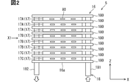
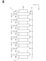
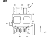
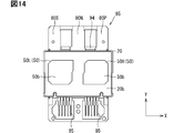
- FIG. 2 is a side view of FIG. 2 as viewed from the X1 direction. It is a top view which shows the semiconductor device which concerns on 1st Embodiment. It is a plan view seen from the side opposite to FIG. It is sectional drawing which follows the VI-VI line shown in FIG. It is sectional drawing which follows the line VII-VII shown in FIG. It is sectional drawing which follows the line VIII-VIII shown in FIG. It is a top view which shows the lead frame. It is a top view which shows the state which arranged the semiconductor element and the terminal.
- the power conversion device can be applied to a moving body whose drive source is a rotary electric machine.
- the moving body is, for example, an electric vehicle such as an electric vehicle (EV), a hybrid vehicle (HV), a fuel cell vehicle (FCV), a vehicle such as a drone, a ship, a construction machine, or an agricultural machine.
- a vehicle hybrid vehicle
- FCV fuel cell vehicle
- the vehicle drive system 1 includes a DC power supply 2, motor generators 3 and 4, and a power conversion device 5 that performs power conversion between the DC power supply 2 and the motor generators 3 and 4. There is.
- the motor generator 3 functions as a generator (alternator) that is driven by an engine (not shown) to generate electricity, and an electric motor (starter) that starts the engine.
- the motor generator 4 functions as a traveling drive source of the vehicle, that is, an electric motor.
- the motor generator 4 functions as a generator during regeneration.
- the vehicle includes an engine and a motor generator 4 as a traveling drive source.
- the power conversion device 5 performs power conversion between the DC power supply 2 and the motor generators 3 and 4.
- the power conversion device 5 includes a filter capacitor C1, a smoothing capacitor C2, a converter 6, inverters 7 and 8, a control circuit unit 9, a drive circuit unit 10, and the like.
- the P line 11 which is a power line on the high potential side has a VL line 11L and a VH line 11H.
- the VL line 11L is connected to the positive electrode terminal of the DC power supply 2.
- a converter 6 is provided between the VL line 11L and the VH line 11H.
- the potential of the VH line 11H is equal to or higher than the potential of the VL line 11L.
- the N line 12 is a power line on the low potential side connected to the negative electrode terminal of the DC power supply 2.
- the N line 12 is sometimes referred to as a ground line.
- the converter 6 is a DC-DC converter.
- the converter 6 converts the DC voltage into a DC voltage having a different value according to the switching control by the control circuit unit 9.
- the converter 6 has a function of boosting the DC voltage supplied from the DC power supply 2.
- the converter 6 also has a step-down function of charging the DC power supply 2 by using the electric charge of the smoothing capacitor C2.
- the converter 6 has an upper and lower arm circuit 6HL and a reactor R1.
- the collector of the switching element Q1 on the upper arm 6H side is connected to the VH line 11H, and the emitter of the switching element Q1 on the lower arm 6L side is connected to the N line 12.
- the emitter of the switching element Q1 on the upper arm 6H side and the collector of the switching element Q1 on the lower arm 6L side are connected to each other.
- One end of the reactor R1 is connected to the VL line 11L, and the other end is connected to the connection points of the upper arm 6H and the lower arm 6L via the booster wiring 13.
- the converter 6 of the present embodiment is configured as a multi-phase converter, specifically, a two-phase converter.
- the converter 6 has a two-phase upper / lower arm circuit 6HL and a reactor R1 provided for each upper / lower arm circuit 6HL.
- Inverters 7 and 8 are DC-AC converters.
- the inverter 7 is connected to the converter 6 via a smoothing capacitor C2.
- the inverter 7 converts the DC voltage into a three-phase AC voltage according to the switching control by the control circuit unit 9, and outputs the DC voltage to the motor generator 3.
- the motor generator 3 is driven so as to generate a predetermined torque.
- the inverter 7 can also convert the three-phase AC voltage generated by the motor generator 3 in response to the output of the engine into a DC voltage according to switching control by the control circuit unit 9 and output it to the VH line 11H. In this way, the inverter 7 performs bidirectional power conversion between the converter 6 and the motor generator 3.
- the inverter 7 has a three-phase (U-phase, V-phase, W-phase) upper and lower arm circuit 7HL.
- the inverter 8 is also connected to the converter 6 via the smoothing capacitor C2.
- the inverter 8 converts the DC voltage into a three-phase AC voltage and outputs it to the motor generator 4 according to the switching control by the control circuit unit 9.
- the motor generator 4 is driven so as to generate a predetermined torque.
- the inverter 8 converts the three-phase AC voltage generated by the motor generator 4 by receiving the rotational force from the drive wheels into a DC voltage according to the switching control by the control circuit unit 9 during the regenerative braking of the vehicle, and shifts to the VH line 11H. It can also be output. In this way, the inverter 8 performs bidirectional power conversion between the converter 6 and the motor generator 4.
- the inverter 8 has a three-phase (U-phase, V-phase, W-phase) upper and lower arm circuit 8HL.
- the control circuit unit 9 generates a drive command for operating the switching elements Q1, Q2, and Q3, and outputs the drive command to the drive circuit unit 10.
- the control circuit unit 9 generates a drive command based on a torque request input from a higher-level ECU (not shown), signals detected by various sensors, and the like.
- the control circuit unit 9 outputs, for example, a PWM signal as a drive command.
- the control circuit unit 9 is configured to include, for example, a microcomputer (microcomputer).
- ECU is an abbreviation for Electronic Control Unit.
- PWM is an abbreviation for Pulse Width Modulation.
- Various sensors include current sensors, rotation angle sensors, voltage sensors, temperature sensors, and the like.
- One of the current sensors detects the phase current flowing through the windings of each phase of the motor generators 3 and 4.
- the other one of the current sensors detects the current flowing through the reactor R1.
- the rotation angle sensor detects the rotation angle of the rotors of the motor generators 3 and 4.
- One of the voltage sensors detects the voltage across the smoothing capacitor C2, that is, the voltage of the VH line 11H.
- the other one of the voltage sensors detects the voltage across the filter capacitor C1, that is, the voltage of the VL line 11L.
- the temperature sensor detects the temperature of the reactor R1.
- the power conversion device 5 has these sensors (not shown).
- the drive circuit unit 10 supplies a drive voltage to the gates of the switching elements Q1, Q2, and Q3 of the corresponding arms 6H, 6L, 7H, 7L, 8H, and 8L based on the drive command of the control circuit unit 9.
- the drive circuit unit 10 drives the corresponding switching elements Q1, Q2, and Q3 by applying a drive voltage, that is, on-drive and off-drive.
- the drive circuit unit 10 may be referred to as a driver.
- one drive circuit unit 10 is provided for one arm.
- the arrangement of the drive circuit unit 10 is not limited to this.
- the drive circuit unit 10 may be provided for each of the upper and lower arm circuits 6HL, 7HL, and 8HL.
- the semiconductor device 17 includes a semiconductor device 17A that constitutes the inverter 7, a semiconductor device 17B that constitutes the inverter 8, and a semiconductor device 17C that constitutes the upper and lower arm circuits 6HL of the converter 6.
- one of the semiconductor devices 17 constitutes one of the upper and lower arm circuits.
- the semiconductor module 16 includes three semiconductor devices 17A constituting a three-phase upper / lower arm circuit 7HL, three semiconductor devices 17B forming a three-phase upper / lower arm circuit 8HL, and a two-phase upper / lower arm circuit 6HL. It includes two semiconductor devices 17C that constitute it.
- the outer contours of the semiconductor devices 17A, 17B, and 17C are substantially equal to each other.
- the cooler 18 is formed by using a metal material having excellent thermal conductivity, for example, an aluminum-based material.
- the cooler 18 includes a heat exchange unit 180, an introduction pipe 181 and a discharge pipe 182.
- the heat exchange unit 180 is housed in a housing.
- the heat exchange unit 180 is a tubular body having a flat shape as a whole.
- the heat exchange unit 180 processes, for example, at least one of a pair of plates (thin metal plates) into a shape bulging in the Z direction by press working. After that, the outer peripheral edges of the pair of plates are fixed to each other by caulking or the like, and are joined to each other by brazing or the like on the entire circumference. As a result, a flow path through which the refrigerant can flow is formed between the pair of plates, and it can be used as the heat exchange unit 180.
- the semiconductor device 17 has a main terminal 80 and a signal terminal 85 as terminals for external connection.
- the main terminal 80 and the signal terminal 85 extend in opposite directions in the Y direction.
- the signal terminal 85 is connected to a circuit board 19 arranged on one side in the Y direction with respect to the laminated body 16a.
- the circuit board 19 is provided so as to overlap all the semiconductor devices 17 constituting the laminated body 16a in a plan view in the Y direction.
- the signal terminal 85 of each semiconductor device 17 is inserted and mounted on the circuit board 19.
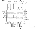
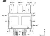
- FIGS. 4, 5, 9, and 11 show structures common to each other in the semiconductor devices 17A, 17B, and 17C.
- the semiconductor element 30 is formed by forming a vertical element on a semiconductor substrate made of silicon (Si), a wide bandgap semiconductor having a wider bandgap than silicon, or the like.
- Examples of wide bandgap semiconductors include silicon carbide (SiC), gallium nitride (GaN), gallium oxide (Ga 2 O 3 ), and diamond.
- the vertical element is configured such that the main current flows in the plate thickness direction of the semiconductor element 30 (semiconductor substrate), that is, in the Z direction.
- the semiconductor element 30 has a gate electrode (not shown).
- the gate electrode has, for example, a trench structure.
- the semiconductor element 30 has main electrodes of the element on both sides in its own plate thickness direction, that is, in the Z direction.
- the collector electrode 31C is provided on one surface side
- the emitter electrode 31E is provided on the back surface side, which is the opposite surface to the one surface.
- the collector electrode 31C also serves as a cathode electrode of the diode.
- the emitter electrode 31E also serves as an anode electrode of the diode.
- the collector electrode 31C corresponds to the first main electrode
- the emitter electrode 31E corresponds to the second main electrode.
- the semiconductor element 30 has a substantially rectangular shape in a plane.
- the semiconductor element 30 has a pad 31P formed at a position different from that of the emitter electrode 31E on the back surface.
- the emitter electrode 31E and the pad 31P are each exposed from a protective film (not shown).
- the collector electrode 31C is formed on almost the entire surface of one surface of the semiconductor element 30.
- the emitter electrode 31E is formed on a part of the back surface of the semiconductor element 30. In plan view, the collector electrode 31C has a larger area than the emitter electrode 31E.
- the emitter electrode 31E has a substantially rectangular shape in a plane.
- the pad 31P is a signal electrode.
- the pad 31P is electrically separated from the emitter electrode 31E.
- the pad 31P is formed at an end portion of the emitter electrode 31E opposite to the forming region in the Y direction.
- the pad 31P is provided alongside the emitter electrode 31E in the Y direction.
- the pad 31P includes at least a pad for a gate electrode.
- the semiconductor element 30 of this embodiment has five pads 31P. Specifically, for the gate electrode, for the Kelvin emitter that detects the potential of the emitter electrode 31E, for the current sense, for the anode potential of the temperature sensor (temperature sensitive diode) that detects the temperature of the semiconductor element 30, and also for the cathode potential. Have.
- the five pads 31P are collectively formed on one end side in the Y direction and are formed side by side in the X direction in the semiconductor element 30 having a substantially rectangular plane.
- the semiconductor device 17B includes a semiconductor element 30H that constitutes the upper arm 7H and a semiconductor element 30L that constitutes the lower arm 7L.
- the two semiconductor elements 30H and 30L have the same configuration as each other.
- the semiconductor elements 30H and 30L are arranged in the X direction.
- the semiconductor elements 30H and 30L are arranged at substantially the same positions as each other in the Z direction.
- the semiconductor device 17C includes a semiconductor element 30H that constitutes the upper arm 8H and a semiconductor element 30L that constitutes the lower arm 8L.
- the two semiconductor elements 30H and 30L have the same configuration as each other.
- the semiconductor elements 30H and 30L are arranged in the X direction.
- the semiconductor elements 30H and 30L are arranged at substantially the same positions as each other in the Z direction.
- the sizes of the semiconductor elements 30 are different from each other.
- the size is the size (area) of the planar shape.
- the semiconductor elements 30H and 30L of the semiconductor devices 17C constituting the converter 6 are larger than the semiconductor elements 30H and 30L of the semiconductor devices 17A and 17B constituting the inverters 7 and 8.
- the semiconductor elements 30H and 30L of the semiconductor device 17A constituting the inverter 7 are smaller than the semiconductor elements 30H and 30L of the semiconductor devices 17B and 17C constituting the inverter 7 and the converter 6.
- the size of the semiconductor element 30 satisfies the relationship of semiconductor device 17A ⁇ semiconductor device 17B ⁇ semiconductor device 17C.
- the size of the emitter electrode 31E satisfies the relationship of semiconductor device 17A ⁇ semiconductor device 17B ⁇ semiconductor device 17C.
- the heat sink 40 is arranged on the collector electrode 31C side of the semiconductor element 30 in the Z direction.
- the heat sink 40 is a wiring member electrically connected to the collector electrode 31C via the solder 90.
- the heat sink 40 corresponds to the first wiring member.
- the heat sink 40 has a facing surface 40a, which is a surface on the semiconductor element 30 side, and a back surface 40b, which is a surface opposite to the facing surface 40a.
- the solder 90 is interposed between the facing surface 40a of the heat sink 40 and the collector electrode 31C of the semiconductor element 30, and a solder joint is formed.
- the heat sink 40 dissipates the heat of the semiconductor element 30 to the outside.
- the heat sink 40 first wiring member
- a metal plate made of Cu, a Cu alloy, or the like, a DBC (Direct Bonded Copper) substrate, or the like can be adopted.
- the heat sink 40 may be provided with a plating film such as Ni or Au on its surface.
- the heat sink 40 of this embodiment is a metal plate made of Cu as a material.
- the heat sink 40 is configured as a part of the lead frame 95.
- the heat sink 40 is a thick portion in the lead frame 95 of the deformed strip.
- the semiconductor device 17 includes two heat sinks 40, respectively.
- the semiconductor device 17 includes a heat sink 40H forming an upper arm and a heat sink 40L forming a lower arm, respectively.
- the heat sinks 40H and 40L have a substantially rectangular shape in a plane.
- the heat sinks 40H and 40L are arranged in the X direction.
- the heat sinks 40H and 40L have substantially the same thickness and are arranged at substantially the same position in the Z direction.
- a joint made of solder 90 is formed between the facing surface 40a of the heat sink 40H and the collector electrode 31C of the semiconductor element 30H, and between the facing surface 40a of the heat sink 40L and the collector electrode 31C of the semiconductor element 30L.
- the heat sink 50 dissipates the heat of the semiconductor element 30 to the outside.
- the heat sink 50 (second wiring member), for example, a metal plate made of Cu, a Cu alloy, or the like, a DBC (Direct Bonded Copper) substrate, or the like can be adopted.
- the heat sink 50 may be provided with a plating film such as Ni or Au on its surface.
- the heat sink 50 of this embodiment is a metal plate made of Cu as a material.
- the heat sink 50 has a facing surface 50a, which is a surface on the semiconductor element 30 side, and a back surface 50b, which is a surface opposite to the facing surface 50a.
- the semiconductor device 17 includes two heat sinks 50, respectively.
- the semiconductor device 17 includes a heat sink 50H forming an upper arm and a heat sink 50L forming a lower arm, respectively.
- connection area 51 is an area of the facing surface 50a surrounded by the groove 52.
- the connection area 51 is an area of a predetermined size (area) defined for electrical connection with the terminal 60.
- the groove 52 defines a connection area 51 inside the groove 52.
- the groove 52 accommodates the excess solder 91.
- the groove 52 is formed in an annular shape, for example.
- the back surface 50b of the heat sinks 50H and 50L is exposed from the sealing resin body 20.
- the back surface 50b may be referred to as a heat radiating surface or an exposed surface.
- the back surface 50b is substantially flush with one surface 20a of the sealing resin body 20.
- the back surfaces 50b of the heat sinks 50H and 50L are arranged in the X direction.
- the terminals 60H and 60L of the present embodiment are substantially rectangular columnar bodies having substantially the same size as the emitter electrode 31E in a plan view. As shown in FIGS. 6, 8 and 10, the size of the terminal 60 satisfies the relationship of semiconductor device 17A ⁇ semiconductor device 17B ⁇ semiconductor device 17C. The positional relationship between the terminal 60 and the groove 52 of the heat sink 50 will be described later.
- the thickness (length in the Z direction) of the terminal 60 is substantially equal to each other in the semiconductor devices 17A, 17B, and 17C.
- the joint portions 70 and 71 connect the elements constituting the upper and lower arm circuits.
- the joint portion connects the elements constituting the semiconductor device 17.
- the joint portion 70 is connected to the heat sink 40L.
- the thickness of the joint portion 70 is thinner than that of the heat sink 40L.
- the joint portion 70 is connected to the facing surface (side surface) of the heat sink 40H in a state of being substantially flush with the facing surface 40a of the heat sink 40L.
- the joint portion 70 has a substantially crank shape in the ZX plane by having two bent portions.
- the joint portion 70 is covered with the sealing resin body 20.
- the joint portion 70 may be provided integrally with the heat sink 40L to be connected, or may be provided as a separate member and may be connected by connection.
- the joint portion 70 of the present embodiment is provided integrally with the heat sink 40L as a part of the lead frame 95.
- the joint portion 71 is connected to the corresponding heat sink 50.
- a joint portion 71 is connected to each of the heat sinks 50H and 50L.
- the thickness of the joint portion 71 is thinner than that of the corresponding heat sink 50.
- the joint portion 71 is covered with the sealing resin body 20.
- the joint portion 71 may be provided integrally with the heat sink 50 to be connected, or may be provided as a separate member and may be connected by connection.
- the joint portion 71 of the present embodiment is provided integrally with the corresponding heat sinks 50H and 50L.
- the joint portion 71 extends in the X direction from the side surfaces facing each other in the two heat sinks 50H and 50L.
- the positive electrode terminal 80P is connected to one end of the heat sink 40H in the Y direction.
- the thickness of the positive electrode terminal 80P is thinner than that of the heat sink 40H.
- the positive electrode terminal 80P is substantially flush with the facing surface 40a and is connected to the heat sink 40H.
- the positive electrode terminals 80P may be provided integrally with the heat sink 40H to be connected, or may be provided as a separate member and connected by connection.
- the positive electrode terminal 80P of this embodiment is provided integrally with the heat sink 40H as a part of the lead frame 95.
- the positive electrode terminal 80P extends in the Y direction from the heat sink 40H and projects outward from the side surface 20c of the sealing resin body 20.
- the positive electrode terminal 80P has a bent portion in the middle of the portion covered by the sealing resin body 20, and projects from the vicinity of the center in the Z direction on the side surface 20c.
- the negative electrode terminal 80N is connected to the joint portion 71 connected to the heat sink 50L.
- a solder 94 is interposed between the facing surfaces of the negative electrode terminal 80N and the joint portion 71 to form a solder joint portion.
- the negative electrode terminal 80N extends in the Y direction and projects from the same side surface 20c as the positive electrode terminal 80P to the outside of the sealing resin body 20.
- the negative electrode terminal 80N has a connecting portion 81 with a joint portion 71 near one end in the Y direction. A part of the negative electrode terminal 80N including the connecting portion 81 is covered with the sealing resin body 20, and the remaining part protrudes from the sealing resin body 20.
- the connecting portion 81 is thicker than the portion protruding from the sealing resin body 20.
- the plate thickness of the connecting portion 81 is substantially the same as that of the heat sink 40, for example.
- the negative electrode terminal 80N also has a bent portion like the main terminal, and projects from the vicinity of the center in the Z direction on the side surface 20c.
- the negative electrode terminal 80N of this embodiment is configured as a part of the lead frame 95.
- the output terminal 80S is connected to one end of the heat sink 40L in the Y direction.
- the thickness of the output terminal 80S is thinner than that of the heat sink 40L.
- the output terminal 80S is substantially flush with the facing surface 40a and is connected to the heat sink 40L.
- the output terminals 80S may be provided integrally with the heat sink 40L to be connected, or may be provided as a separate member and connected by connection.
- the output terminal 80S of this embodiment is provided integrally with the heat sink 40L as a part of the lead frame 95.
- the output terminal 80S extends from the heat sink 40L in the Y direction, and projects from the same side surface 20c as the positive electrode terminal 80P to the outside of the sealing resin body 20.
- the output terminal 80S also has a bent portion like the positive electrode terminal 80P, and projects from the vicinity of the center in the Z direction on the side surface 20c.
- the three main terminals 80 are arranged in the order of the positive electrode terminal 80P, the negative electrode terminal 80N, and the output terminal 80S in the X direction.
- the signal terminal 85 is electrically connected to the pad 31P of the corresponding semiconductor element 30. In this embodiment, they are electrically connected via the bonding wire 96.
- the signal terminal 85 extends in the Y direction and projects outward from the side surface 20d of the sealing resin body 20.
- the side surface 20d is a surface opposite to the side surface 20c in the Y direction. In this embodiment, five signal terminals 85 are provided for one semiconductor element 30.
- the inner lead portion arranged inside the sealing resin body 20 has a crank shape as shown in FIGS. 9 and 10.
- the positions of the connecting portion of the bonding wire 96 and the sealing end portion on the side surface 20d are deviated in the X direction.
- the connecting portion of the bonding wire 96 is closer to the corresponding semiconductor element 30 (pad 31P) in the X direction than the sealing end portion on the side surface 20d.
- Reference numeral 97 shown in FIG. 5 and the like is a hanging lead.
- the heat sink 40 (40H, 40L), the joint portion 70, the main terminal 80, and the signal terminal 85 are configured in a lead frame 95 which is a common member.
- the lead frame 95 is a deformed strip having a partially different thickness.
- the signal terminal 85 is connected to the suspension lead 97 via the tie bar 98 in the state before cutting. Unnecessary parts of the lead frame 95, such as the tie bar 98, are cut (removed) after molding the sealing resin body 20.
- a plurality of semiconductor elements 30 constituting the upper and lower arm circuits for one phase are sealed by the sealing resin body 20.
- the sealing resin body 20 integrates a plurality of semiconductor elements 30, a part of each of the heat sinks 40, a part of each of the heat sinks 50, a terminal 60, joints 70 and 71, a part of each of the main terminals 80 and the signal terminal 85. Is sealed.
- the lead frame 95 shown in FIG. 9 is prepared.
- a laminate in which the semiconductor element 30 and the terminal 60 are arranged is formed on the heat sink 40.
- the molten solder 90 is applied on the facing surface 40a of the heat sink 40, and the semiconductor element 30 is arranged on the molten solder 90 so that the collector electrode 31C is on the facing surface 40a side.
- the molten solder 92 is applied onto the emitter electrode 31E of the semiconductor element 30, and the terminal 60 is arranged on the molten solder 92.
- the molten solder 91 is applied onto the end face 60b of the terminal 60.
- the molten solders 93 and 94 are also applied on the joint portion 70 and the connection portion 81.
- the molten solders 90 to 94 can be applied, for example, by using a transfer method.
- a laminated body is obtained by solidifying (solidifying) the applied molten solders 90 and 92.
- the molten solders 90 to 94 may be solidified (solidified) in the order of lamination, or all of them may be solidified (solidified) at once.
- the bonding wire 96 may be connected after the laminated body is formed, or may be performed after the molten solder 90 is solidified and before the molten solder 92 is applied on the emitter electrode 31E.
- the semiconductor device 17 having a double-sided heat dissipation structure is sandwiched from both sides in the Z direction by the heat exchange portion 180 of the cooler 18 as described above. Therefore, high parallelism of the surfaces and high dimensional accuracy between the surfaces are required in the Z direction. Therefore, for the solder 91, an amount capable of absorbing the height variation of the semiconductor device 17 is arranged. That is, more solder 91 is arranged than the solder 90 and 92. The same applies to the solders 93 and 94.
- the laminate and the heat sink 50 are connected.
- the heat sink 50 is arranged on a pedestal (not shown) so that the facing surface 50a faces up.
- the laminate is arranged on the heat sink 50 so that the end surface 60b of the terminal 60, that is, the solder 91 faces the facing surface 50a, and reflow is performed.
- a load is applied from the heat sink 40 side in the Z direction so that the height of the semiconductor device 17 becomes a predetermined height.
- a spacer (not shown) is brought into contact with both the facing surface 40a of the heat sink 40 and the mounting surface of the pedestal. In this way, the height of the semiconductor device 17 is set to a predetermined height.
- the sealing resin body 20 is molded by the transfer molding method.
- the sealing resin body 20 is molded so that the heat sinks 40 and 50 are completely covered.
- the resin 21 is injected from the gate 102 into the cavity 101 of the molding die 100.
- the gate 102 is connected to the side surface forming the cavity 101 on the semiconductor element 30H side.
- the gate 102 is connected to the cavity 101 in the vicinity of the connecting portion between the heat sink 40H and the suspension lead 97.
- Mold 100 has a flow cavity 103.
- the flow cavity 103 is connected to the cavity 101 that forms the sealing resin body 20.
- the flow cavity 103 is connected to the side surface of the wall surface forming the cavity 101 opposite to the gate 102.
- the flow cavity 103 is provided on the signal terminal 85 side in the Y direction.
- FIG. 15 shows the positional relationship between the terminal 60 and the groove 52 in each of the semiconductor devices 17A, 17B, and 17C.
- an end surface 60b which is a surface facing the heat sink 50, is shown in order to show the positional relationship.
- the end face 60b has a substantially rectangular shape in a plane. As shown in FIG. 15, the end face 60b has two sides 61a and 61b substantially parallel to the X direction and two sides 61c and 61d substantially parallel to the Y direction as outer peripheral end portions. The end face 60b may have R portions at the four corners, or may have no R portions.
- the side 61a is provided on the signal terminal 85 side, that is, the pad 31P side
- the side 61b is provided on the main terminal 80 side.
- the side 61c is provided on the joint portion side
- the side 61d is provided outside the side 61c in the X direction.
- the groove 52 of the heat sink 50 has a common configuration in the semiconductor devices 17A, 17B, and 17C. That is, they are configured to match each other in a plan view. Due to the common use of the grooves 52, the heat sink 50 is a common component in the semiconductor devices 17A, 17B, and 17C.
- the size of the groove 52 is set according to the largest terminal 60 in the semiconductor devices 17A, 17B, and 17C constituting the power conversion unit. In this embodiment, the terminal 60 of the semiconductor device 17C constituting the converter 6 is the largest.
- the size of the groove 52 is set so that the terminal 60 of the semiconductor device 17C fits in the plan view.
- the groove 52 is provided so as to overlap only one or only two of the four sides 61a, 61b, 61c, and 61d of the end face 60b in a plan view.
- the groove 52 of the present embodiment has a substantially rectangular annular shape in a plane.
- the groove 52 has two extending portions 52a and 52b extending substantially parallel to the X direction and two extending portions 52a and 52b extending substantially parallel to the Y direction.
- the extension portion 52a is provided on the signal terminal 85 side, that is, the pad 31P side
- the extension portion 52b is provided on the main terminal 80 side.
- the extension portion 52c is provided on the joint portion side
- the extension portion 52d is provided outside the extension portion 52c.
- the groove 52 may have R portions at the four corners of the rectangle, or may have no R portion.
- the groove 52 is provided unevenly with respect to the terminal 60 in the Y direction. Specifically, in the Y direction, the distance between the side 61a on the pad 31P side and the extension portion 52a is shorter than the distance between the side 61b on the opposite side and the extension portion 52b. As described above, the groove 52 is provided so that the side 61a on the pad 31P side is closer to the groove 52 than the side 61b on the opposite side. In other words, the center of the groove 52 does not coincide with the center of the terminal 60 and is deviated in the direction away from the pad 31P. Therefore, the terminals 60 are arranged unevenly toward the side 61a in the Y direction.
- the semiconductor devices 17A, 17B, and 17C form a non-overlapping region 51a in which the terminal 60 does not overlap between the side 61b of the end surface 60b and the extension portion 52b of the groove 52 as a part of the connection region 51.
- the distance L1 between the side 61a on the pad 31P side and the extension portion 52a is shorter than the distance L2 between the side 61b on the opposite side and the extension portion 52b. The same applies to the other semiconductor devices 17A and 17B.
- the extending portion 52a of the groove 52 overlaps with the side 61a of the end face 60b.
- the groove 52 does not overlap the sides 61b, 61c, 61d.
- the sides 61b, 61c, and 61d overlap with the connection area 51.
- the groove 52 of the heat sink 50 overlaps the side 61a on the pad 31P side of the end surface 60b and does not overlap the side 61b on the opposite side.
- the groove 52 overlaps only the side 61a.
- the groove 52 is designed so that a plurality of types of terminals 60 having different sizes can be accommodated.
- the groove 52 is not provided so as to overlap all of the four sides 61a, 61b, 61c, 61d of the end face 60b of the terminal 60, but only one of the four sides 61a, 61b, 61c, 61d.
- it is provided in a size that overlaps only two.
- excess solder 91 can be accommodated in the grooves 52 having a common configuration for the plurality of terminals 60 having different sizes.
- the heat sink 50 can be used as a common component.
- the semiconductor device 17 of the present embodiment it is possible to reduce the types of parts (product numbers) while accommodating the surplus solder 91. Thereby, the cost can be reduced. Further, by standardizing the heat sink 50, the mold forming the groove 52 can also be standardized. As a result, the manufacturing cost can be reduced.
- the power conversion device 5 of the present embodiment includes a plurality of types of semiconductor devices 17A, 17B, and 17C that form different power conversion units.
- the semiconductor devices 17A, 17B, and 17C the sizes of the semiconductor element 30 and the terminal 60 are different from each other.
- the structure of the groove 52 is common.
- the heat sink 50 can be used as a common component.
- the groove 52 having the common configuration has a size that overlaps with only one or only two of the four sides 61a, 61b, 61c, 61d of the end face 60b of the terminal 60. There is.
- the surplus solder 91 can be accommodated in the groove 52. From the above, it is possible to reduce the types of parts in the power conversion device 5.
- the power conversion device 5 includes a semiconductor device 17A that constitutes the inverter 7, a semiconductor device 17B that constitutes the inverter 8, and a semiconductor device 17C that constitutes the converter 6. That is, three types of semiconductor devices 17 (17A, 17B, 17C) having different sizes of the semiconductor element 30 and the terminal 60 are provided. Of the three types of semiconductor devices 17, one of any two types corresponds to the first semiconductor device, and the other corresponds to the second semiconductor device.
- the power conversion unit composed of the first semiconductor device corresponds to the first power conversion unit, and the power conversion unit composed of the second semiconductor device corresponds to the second power conversion unit.
- the semiconductor device 17A corresponds to the first semiconductor device
- the semiconductor device 17C corresponds to the second semiconductor device.
- the inverter 7 corresponds to the first power conversion unit
- the converter 6 corresponds to the second conversion unit.
- FIG. 16 is a cross-sectional view showing the effect of the arrangement of the grooves 52 of the present embodiment, and also shows a reference example.
- the elements that are the same as or related to the elements of the present embodiment are shown by adding r to the end of the reference numerals of the present embodiment.
- the groove 52r does not overlap with the sides 61ar and 61r of the end face 60br of the terminal 60r.
- the sides 61ar and 61r overlap with the connection area 51r.
- the molten solder 91r is pushed from the laminate side and flows around the end surface 60br.
- the groove 52r is recessed with respect to the substantially flat connection region 51r, and when the solder 91 wets and spreads from the connection region 51r to the groove 52r, it stays at the interface not a little due to surface tension. Therefore, the solder 91 rises around the end face 60br.
- the solder 91r is closer to the semiconductor element 30r than the end face 60br in the Z direction. Therefore, the raised portion of the solder 91r may come into contact with the bonding wire 96r. Further, the solder 91r may come into contact with the side surface of the terminal 60r.
- the groove 52 is provided so as to overlap the side 61a on the pad 31P side of the end surface 60b and not to overlap the side 61b on the opposite side. There is. Even if the molten solder 91 is pushed from the laminate side and flows around the end face 60b during reflow, it is accommodated in the groove 52 on the pad 31P side. As a result, it is possible to suppress the formation of a raised portion of the solder 91 on the pad 31P side. Therefore, it is possible to prevent the solder 91 from coming into contact with the bonding wire 96.
- the solder 91 since a part of the solder 91 is accommodated in the groove 52, it flows around the end face 60b, and the solder 91 located on the connection region 51 is reduced. As a result, the swelling of the solder 91 can be suppressed on the side opposite to the pad 31P. Even if there is a bulge, the height will be low. Therefore, it is possible to prevent the solder 91 from coming into contact with the side surface of the terminal 60.
- connection region 51 has a non-overlapping region 51a between the side 61b and the extension portion 52b of the groove 52. Therefore, the solder 91 pushed around the end face 60b wets and spreads in the non-overlapping region 51a. The swelling of the solder 91 can be suppressed by the wet spread.
- the groove 52 is provided so as to overlap the sides 61c and 61d at both ends in the X direction on the end surface 60b.
- the terminal 60 of the semiconductor device 17C is the largest, but the solder 91 pushed around the end face 60b during reflow can be accommodated in the grooves 52 (extended portions 52c, 52d) on both sides in the X direction. Thereby, for example, it is possible to prevent the solder 91 from spreading on the side surface side of the terminal 60.
- the arrangement of the grooves 52 is biased in the Y direction with respect to the terminal 60.
- the distance L1 between the side 61a on the pad 31P side and the extension portion 52a is biased so as to be shorter than the distance L2 between the side 61b on the opposite side and the extension portion 52b.
- the solder 91 pressed around the end face 60b during reflow is likely to be accommodated in the groove 52 on the pad 31P side.
- This embodiment is a modification based on the preceding embodiment, and the description of the preceding embodiment can be incorporated.
- a groove 52 for accommodating the excess solder 91 is provided on the facing surface 50a of the heat sink 50. Further, the structure may be configured to prevent the solder from overflowing to the outside of the groove 52.
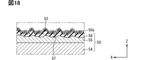
- FIG. 17 shows the facing surface 50a of the heat sink 50 in the semiconductor device 17 according to the present embodiment.
- FIG. 17 illustrates a heat sink 50H and a terminal 60H on the upper arm side of the semiconductor device 17B.
- the heat sink 50L and the terminal 60L on the lower arm side have the same configuration.
- the semiconductor devices 17A and 17C have the same configuration.
- FIG. 18 is a cross-sectional view taken along the line XVIII-XVIII of FIG.
- the heat sink 50 has a base material 54, a metal film 55 provided on the surface of the base material 54, and an uneven oxide film 56.
- the base material 54 forms a main part of the heat sink 50.
- the base material 54 is formed by using a Cu-based material.
- the metal film 55 is formed containing a material having a higher wettability to the solder 91 than the base material 54.
- the metal film 55 is formed over the entire surface of the facing surface 50a.
- the uneven oxide film 56 is locally formed on the facing surface 50a.
- the uneven oxide film 56 is locally formed on the metal film 55 on the facing surface 50a by irradiating the metal film 55 with a laser beam.
- the metal film 55 is provided on the surface of the base material 54 excluding, for example, the back surface 50b.
- the metal film 55 has a base film containing Ni (nickel) as a main component and an upper ground film containing Au (gold) as a main component.
- an electroless Ni plating film containing P (phosphorus) is used as the base film.
- the upper ground film (Au) of the portion in contact with the solder 91 diffuses into the solder 91 during reflow.
- Reference numeral 57 shown in FIG. 18 is a recess formed on the surface of the metal film 55.
- the recess 57 is formed by irradiating a pulsed laser beam. One recess 57 is formed for each pulse.
- the uneven oxide film 56 is formed by melting, vaporizing, and depositing the surface layer portion of the metal film 55 by irradiation with laser light.
- the uneven oxide film 56 is an oxide film derived from the metal film 55.
- the concave-convex oxide film 56 is a film of an oxide of a metal (Ni) as a main component of the metal film 55.
- the uneven oxide film 56 is formed following the unevenness of the surface of the metal film 55 having the concave portions 57. On the surface of the uneven oxide film 56, unevenness is formed at a pitch finer than the width of the concave portion 57. That is, very fine unevenness (roughened portion) is formed.
- the laser beam is scanned so that the spots of the adjacent laser beams partially overlap in the X direction and the spots of the adjacent laser beams partially overlap in the Y direction.
- the laser beam is scanned in the X direction from the reference coordinates in the X direction to irradiate the first row.
- the coordinates in the Y direction may be shifted, the laser beam may be scanned in the X direction from the reference coordinates in the X direction, and the irradiation in the second row may be performed.
- the laser beam is scanned in the opposite direction in the X direction to perform the irradiation in the second row.
- the back scan is performed without waiting for the return to the reference coordinates.
- the irradiation time of the laser beam can be shortened.
- the spot 105 in the first row and the spot 105 in the second row are shifted in the X direction. Specifically, in the X direction, the position of the spot 105 is shifted so that the center position between the two adjacent spots 105 in the first row and the center position of the spot 105 in the second row substantially coincide with each other.
- the portion of the molten metal film 55 is solidified. Specifically, the molten and vaporized metal film 55 is vapor-deposited on the portion irradiated with the laser beam and the peripheral portion thereof. By depositing the molten and vaporized metal film 55 in this way, the uneven oxide film 56 is formed on the surface of the metal film 55. As described above, the staggered arrangement of the spots 105 (staggered arrangement) can reduce the variation in the formation of the uneven oxide film 56 over the entire roughened region 53. That is, the film thickness of the uneven oxide film 56 per unit area can be made substantially uniform over the entire area of the roughened region 53. As described above, the heat sink 50 is prepared.
- the groove 52 is provided so as to overlap only one or only two of the four sides 61a, 61b, 61c, 61d of the end face 60b of the terminal 60.
- the groove 52 overlaps only the side 61a, even if the excess solder 91 cannot be accommodated (absorbed) only by the extending portion 52a overlapping the side 61a, the groove is formed by the roughened region 53 (concave and convex oxide film 56). Wet spread to the outside of 52 is suppressed.
- the excess solder 91 wets and spreads in the groove 52 toward the extending portions 52c and 52d, as shown by the arrow of the alternate long and short dash line in FIG. Therefore, by standardizing the grooves 52, it is possible to prevent the solder 91 from overflowing to the outside of the grooves 52 in a configuration in which the heat sink 50 is a common component. The same applies to the configuration in which the groove 52 overlaps only the sides 61c and 61d.
- ⁇ Modification example> In the present embodiment, an example is shown in which the entire region outside the groove 52 is the roughened region 53 on the facing surface 50a of the heat sink 50, but the present invention is not limited to this.
- a roughened region 53 may be provided only in a part of the region outside the groove 52 so as to surround the groove 52.
- the region outside the groove 52 and excluding the edge region 58 may be the roughened region 53.
- the roughened region 53 is hatched for clarification.
- the edge region 58 is an region including the outer peripheral end of the facing surface 50a.
- a roughened region may be provided on the formation surface of the groove 72 in the joint portion 71.
- the roughened region is formed by irradiation with a laser beam as in the roughened region 53.
- the roughened region is provided on the outside of the groove 72 in the joint portion 71 so as to surround the groove 72.
- the roughened region of the joint portion 71 may be provided so as to be continuous with the roughened region 53 of the heat sink 50.
- a roughened region 62 may be provided on the side surface of the terminal 60.
- the roughened region 62 is provided on almost the entire side surface.
- the roughened region 62 is formed by irradiation with a laser beam.
- the terminal 60 also has a base material, a metal film provided on the base material, and an uneven oxide film.
- the straightening jig 107 shown in FIG. 22 corrects the position of the signal terminal 85, particularly the position of the tip to be inserted. Specifically, the straightening jig 107 is pressed near the tip of the signal terminal 85 to apply a load to the signal terminal 85 to deform it. After that, the signal terminal 85 springs back by releasing the load from the straightening jig 107. As a result, the tip positions of the plurality of signal terminals 85 are corrected.
- the roughened region 86 is hatched for clarification. Like the roughened region 53, the roughened region 86 is formed by irradiation with a laser beam.
- the signal terminal 85 also has a base material, a metal film provided on the base material, and an uneven oxide film. In the roughened region 86, the film thickness of the metal film (Ni plating film) is thinner than that in the non-irradiated area.
- the roughened region 86 becomes the starting point of plating cracks. That is, the signal terminal 85 is deformed starting from the roughened region 86. In this way, since the starting point is stable, it is possible to reduce variations in the tip position after correction.
- the roughened region 86 is not limited to the root portion of the outer lead portion.
- a roughened region 86 may be provided from the outer lead portion to the inner lead portion.
- the roughened region 86 is formed so as to avoid the connecting portion of the bonding wire 96.
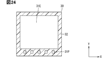
- FIG. 24 is a plan view showing the configuration of the back surface side of the semiconductor element 30 in the semiconductor device 17 according to the present embodiment.
- the semiconductor element 30 has a protective film 32.
- the protective film 32 is hatched in FIG. 24, which is a plan view.
- the constituent material of the protective film 32 is, for example, polyimide.
- the protective film 32 is provided on the back surface of the semiconductor substrate around the emitter electrode 31E and the pad 31P.
- the emitter electrode 31E and the pad 31P are exposed from the opening of the protective film 32.
- the protective film 32 is an insulating film provided on the emitter electrode 31E side and forming a part of the surface of the semiconductor element 30.
- the solder 92 is connected to the emitter electrode 31E.
- a bonding wire 96 is connected to the pad 31P.
- the sealing resin body 20 is in close contact with the protective film 32.
- FIG. 25 is a diagram showing the relationship between the arithmetic mean roughness Ra of the surface of the protective film 32 and the bulk fracture rate.
- FIG. 25 shows the test results. As shown in FIG. 25, when the arithmetic mean roughness Ra was set to 8 nm or more, bulk fracture occurred with a probability of 100%. On the other hand, below 8 nm, interfacial fracture and combined fracture of interfacial fracture and bulk fracture were observed, and the bulk fracture rate was less than 100%. Based on this finding, in the present embodiment, the surface of the protective film 32 is intentionally roughened so that the arithmetic mean roughness Ra is 8 nm or more.
- the surface of the protective film 32 can be roughened by, for example, ashing.
- Ashing is a process in which the surface of a resin is irradiated with oxygen plasma in a high energy state, combined with carbon constituting the resin, and vaporized and decomposed (ashed: ashing) as CO 2.
- the semiconductor device 30 of the present embodiment has a protective film 32 having an arithmetic average roughness Ra of 8 nm or more on the surface.
- Ra arithmetic average roughness
- polyimide is shown as the protective film 32, but the present invention is not limited to this.
- An insulating film other than polyimide for example, a silicon oxide film, a silicon nitride film, a PSG (Phospho Silicate Glass) film, or the like may be used as the protective film 32. By intentionally roughening the surface of these insulating films, peeling of the sealing resin body 20 can be suppressed.
- the spatially relative terms “inside”, “outside”, “back”, “bottom”, “low”, “top”, “high”, etc. are one element or feature as illustrated. It is used herein to facilitate descriptions that describe the relationship to other elements or features. Spatial relative terms can be intended to include different orientations of the device in use or operation, in addition to the orientations depicted in the drawings. For example, when the device in the figure is flipped over, an element described as “below” or “directly below” another element or feature is directed “above” the other element or feature. Therefore, the term “down” can include both up and down orientations. The device may be oriented in the other direction (rotated 90 degrees or in any other direction) and the spatially relative descriptors used herein are interpreted accordingly. ..
- the control circuit unit 9 and the drive circuit unit 10 are provided by a control system including at least one computer.
- the control system includes at least one processor (hardware processor) which is hardware.
- the hardware processor can be provided by (i), (ii), or (iii) below.
- the hardware processor may be a hardware logic circuit.
- the computer is provided by a digital circuit that includes a large number of programmed logic units (gate circuits).
- Digital circuits may include memory for storing programs and / or data.
- Computers may be provided by analog circuits.
- Computers may be provided by a combination of digital and analog circuits.
- the hardware processor may be at least one processor core that executes a program stored in at least one memory.
- the computer is provided by at least one memory and at least one processor core.
- the processor core is referred to as, for example, a CPU.
- Memory is also referred to as a storage medium.
- a memory is a non-transitional and substantive storage medium that non-temporarily stores "programs and / or data" that can be read by a processor.
- the hardware processor may be a combination of the above (i) and the above (ii). (I) and (ii) are arranged on different chips or on a common chip.
- control circuit unit 9 and the drive circuit unit 10 can be provided by hardware only, software only, or a combination thereof.
- the power conversion device 5 includes a control circuit unit 9, but the present invention is not limited to this.
- the configuration may not include the control circuit unit 9.
- the drive circuit unit 10 is provided for each arm has been shown, but the present invention is not limited to this.
- one drive circuit unit 10 may be provided for one upper and lower arm circuit.
- the vehicle drive system 1 is not limited to the above configuration.
- an example including two motor generators 3 and 4 is shown, but the present invention is not limited thereto.
- An example is shown in which the power conversion device 5 includes a converter 6 and inverters 7 and 8 as a power conversion unit, but the present invention is not limited thereto.
- a plurality of power converters may be provided.
- it may be configured to include only a plurality of inverters. It may be configured to include one inverter and a converter.
- the power conversion device 5 includes semiconductor devices 17A, 17B, and 17C, but the present invention is not limited thereto.
- the number of layers of the semiconductor device 17 in the semiconductor module 16 is not limited to the above example.
- the semiconductor element 30 has an RC-IGBT element, but the present invention is not limited to this.
- the switching elements Q1, Q2, and Q3 and the diodes D1, D2, and D3 may be used as separate chips (different semiconductor elements).
- An example of the IGBT is shown as the switching elements Q1, Q2, and Q3, but the present invention is not limited to this.
- MOSFET can be adopted.
- a plurality of semiconductor elements 30H may be provided, and a plurality of semiconductor elements 30H may be connected in parallel to form one of the upper arms.
- a plurality of semiconductor elements 30L may be provided, and a plurality of semiconductor elements 30L may be connected in parallel to form one of the lower arms.
- the back surfaces 40b and 50b of the heat sinks 40 and 50 are exposed from the sealing resin body 20, but the present invention is not limited to this. At least one of the back surfaces 40b and 50b may be covered with the sealing resin body 20. At least one of the back surfaces 40b and 50b may be covered with an insulating member (not shown) different from the sealing resin body 20.
- the semiconductor device 17 includes a sealing resin body 20, but the present invention is not limited to this. The configuration may not include the sealing resin body 20.
- the semiconductor device 17 includes a plurality of semiconductor elements 30 that form an upper and lower arm circuit for one phase, but the present invention is not limited to this. Only the semiconductor element 30 constituting one arm may be provided.
- the semiconductor device 17 includes, for example, a semiconductor element 30 constituting one arm, a pair of heat sinks 40 and 50 arranged so as to sandwich the semiconductor element 30, and a terminal 60 interposed between the semiconductor element 30 and the heat sink 50. You just have to prepare. Further, the semiconductor elements constituting the upper and lower arm circuits of a plurality of phases may be provided as one package.
Landscapes
- Engineering & Computer Science (AREA)
- Power Engineering (AREA)
- Inverter Devices (AREA)
- Physics & Mathematics (AREA)
- Geometry (AREA)
- Cooling Or The Like Of Semiconductors Or Solid State Devices (AREA)
Priority Applications (3)
| Application Number | Priority Date | Filing Date | Title |
|---|---|---|---|
| CN202511189938.7A CN121054592A (zh) | 2020-05-01 | 2021-03-12 | 半导体装置 |
| CN202180031629.0A CN115516624B (zh) | 2020-05-01 | 2021-03-12 | 半导体装置及电力变换装置 |
| US17/976,370 US12581946B2 (en) | 2020-05-01 | 2022-10-28 | Semiconductor device and power converter |
Applications Claiming Priority (2)
| Application Number | Priority Date | Filing Date | Title |
|---|---|---|---|
| JP2020081437A JP7452233B2 (ja) | 2020-05-01 | 2020-05-01 | 半導体装置および電力変換装置 |
| JP2020-081437 | 2020-05-01 |
Related Child Applications (1)
| Application Number | Title | Priority Date | Filing Date |
|---|---|---|---|
| US17/976,370 Continuation US12581946B2 (en) | 2020-05-01 | 2022-10-28 | Semiconductor device and power converter |
Publications (1)
| Publication Number | Publication Date |
|---|---|
| WO2021220641A1 true WO2021220641A1 (ja) | 2021-11-04 |
Family
ID=78300530
Family Applications (1)
| Application Number | Title | Priority Date | Filing Date |
|---|---|---|---|
| PCT/JP2021/010172 Ceased WO2021220641A1 (ja) | 2020-05-01 | 2021-03-12 | 半導体装置および電力変換装置 |
Country Status (4)
| Country | Link |
|---|---|
| US (1) | US12581946B2 (https=) |
| JP (1) | JP7452233B2 (https=) |
| CN (2) | CN115516624B (https=) |
| WO (1) | WO2021220641A1 (https=) |
Cited By (1)
| Publication number | Priority date | Publication date | Assignee | Title |
|---|---|---|---|---|
| US20220278030A1 (en) * | 2019-12-12 | 2022-09-01 | Denso Corporation | Semiconductor device |
Families Citing this family (1)
| Publication number | Priority date | Publication date | Assignee | Title |
|---|---|---|---|---|
| JP7689653B2 (ja) * | 2022-02-17 | 2025-06-09 | 株式会社デンソー | 半導体装置 |
Citations (3)
| Publication number | Priority date | Publication date | Assignee | Title |
|---|---|---|---|---|
| JP2015053343A (ja) * | 2013-09-05 | 2015-03-19 | トヨタ自動車株式会社 | 半導体装置 |
| JP2019176058A (ja) * | 2018-03-29 | 2019-10-10 | 株式会社デンソー | 半導体装置 |
| JP2020031129A (ja) * | 2018-08-22 | 2020-02-27 | トヨタ自動車株式会社 | 半導体装置 |
Family Cites Families (10)
| Publication number | Priority date | Publication date | Assignee | Title |
|---|---|---|---|---|
| JP4702196B2 (ja) | 2005-09-12 | 2011-06-15 | 株式会社デンソー | 半導体装置 |
| JP2011222675A (ja) * | 2010-04-07 | 2011-11-04 | Mitsubishi Electric Corp | 半導体装置及びその製造方法 |
| JP6228490B2 (ja) * | 2014-03-04 | 2017-11-08 | ローム株式会社 | 半導体装置および半導体装置の製造方法 |
| JP6578900B2 (ja) * | 2014-12-10 | 2019-09-25 | 株式会社デンソー | 半導体装置及びその製造方法 |
| WO2016092791A1 (ja) * | 2014-12-10 | 2016-06-16 | 株式会社デンソー | 半導体装置およびその製造方法 |
| US10038307B2 (en) * | 2014-12-19 | 2018-07-31 | Alpes Lasers Sa | Quantum cascade laser optimized for epitaxial side-down mounting |
| JP6485398B2 (ja) * | 2016-04-13 | 2019-03-20 | 株式会社デンソー | 電子装置及びその製造方法 |
| JP6696480B2 (ja) * | 2017-03-22 | 2020-05-20 | 株式会社デンソー | 半導体装置 |
| JP2019153752A (ja) * | 2018-03-06 | 2019-09-12 | トヨタ自動車株式会社 | 半導体装置 |
| JP7106891B2 (ja) * | 2018-03-06 | 2022-07-27 | 株式会社デンソー | 半導体装置 |
-
2020
- 2020-05-01 JP JP2020081437A patent/JP7452233B2/ja active Active
-
2021
- 2021-03-12 CN CN202180031629.0A patent/CN115516624B/zh active Active
- 2021-03-12 WO PCT/JP2021/010172 patent/WO2021220641A1/ja not_active Ceased
- 2021-03-12 CN CN202511189938.7A patent/CN121054592A/zh active Pending
-
2022
- 2022-10-28 US US17/976,370 patent/US12581946B2/en active Active
Patent Citations (3)
| Publication number | Priority date | Publication date | Assignee | Title |
|---|---|---|---|---|
| JP2015053343A (ja) * | 2013-09-05 | 2015-03-19 | トヨタ自動車株式会社 | 半導体装置 |
| JP2019176058A (ja) * | 2018-03-29 | 2019-10-10 | 株式会社デンソー | 半導体装置 |
| JP2020031129A (ja) * | 2018-08-22 | 2020-02-27 | トヨタ自動車株式会社 | 半導体装置 |
Cited By (2)
| Publication number | Priority date | Publication date | Assignee | Title |
|---|---|---|---|---|
| US20220278030A1 (en) * | 2019-12-12 | 2022-09-01 | Denso Corporation | Semiconductor device |
| US12476172B2 (en) * | 2019-12-12 | 2025-11-18 | Denso Corporation | Semiconductor device |
Also Published As
| Publication number | Publication date |
|---|---|
| JP2021176177A (ja) | 2021-11-04 |
| JP7452233B2 (ja) | 2024-03-19 |
| CN115516624A (zh) | 2022-12-23 |
| US12581946B2 (en) | 2026-03-17 |
| CN121054592A (zh) | 2025-12-02 |
| US20230040316A1 (en) | 2023-02-09 |
| CN115516624B (zh) | 2025-09-02 |
Similar Documents
| Publication | Publication Date | Title |
|---|---|---|
| JP5437943B2 (ja) | パワー半導体ユニット、パワーモジュールおよびそれらの製造方法 | |
| US10692792B2 (en) | Electronic device | |
| CN103081104B (zh) | 功率半导体模块及其制造方法 | |
| WO2012090666A1 (ja) | 電力変換装置 | |
| US9165848B2 (en) | Semiconductor device | |
| US20240421132A1 (en) | Semiconductor device | |
| JP2020156310A (ja) | パワーモジュール及び電力変換装置 | |
| US20240079383A1 (en) | Semiconductor device | |
| CN121335181A (zh) | 半导体装置 | |
| JP7852779B2 (ja) | 半導体装置 | |
| US12581946B2 (en) | Semiconductor device and power converter | |
| CN118696411A (zh) | 半导体装置 | |
| CN117157759A (zh) | 半导体装置 | |
| US20240213123A1 (en) | Semiconductor device | |
| US20230223310A1 (en) | Element package and semiconductor device | |
| JP7363682B2 (ja) | 半導体装置 | |
| JP7327134B2 (ja) | 半導体装置 | |
| JP2023013642A (ja) | 半導体装置 | |
| JP7771864B2 (ja) | 半導体装置およびその製造方法 | |
| JP2023078915A (ja) | 半導体装置およびその製造方法 | |
| WO2025263250A1 (ja) | 半導体モジュールおよび電力変換装置 | |
| JP2023183160A (ja) | 半導体装置およびその製造方法 | |
| JP2025185600A (ja) | 半導体装置 | |
| JP2021129385A (ja) | 電力変換器及びその製造方法 |
Legal Events
| Date | Code | Title | Description |
|---|---|---|---|
| 121 | Ep: the epo has been informed by wipo that ep was designated in this application |
Ref document number: 21797554 Country of ref document: EP Kind code of ref document: A1 |
|
| NENP | Non-entry into the national phase |
Ref country code: DE |
|
| 122 | Ep: pct application non-entry in european phase |
Ref document number: 21797554 Country of ref document: EP Kind code of ref document: A1 |
|
| WWG | Wipo information: grant in national office |
Ref document number: 202180031629.0 Country of ref document: CN |