WO2021205958A1 - アミジナート化合物、その二量体化合物、薄膜形成用原料及び薄膜の製造方法 - Google Patents
アミジナート化合物、その二量体化合物、薄膜形成用原料及び薄膜の製造方法 Download PDFInfo
- Publication number
- WO2021205958A1 WO2021205958A1 PCT/JP2021/013898 JP2021013898W WO2021205958A1 WO 2021205958 A1 WO2021205958 A1 WO 2021205958A1 JP 2021013898 W JP2021013898 W JP 2021013898W WO 2021205958 A1 WO2021205958 A1 WO 2021205958A1
- Authority
- WO
- WIPO (PCT)
- Prior art keywords
- atom
- compound
- thin film
- group
- raw material
- Prior art date
- Legal status (The legal status is an assumption and is not a legal conclusion. Google has not performed a legal analysis and makes no representation as to the accuracy of the status listed.)
- Ceased
Links
- 0 *C1N(*)NC(*)(*)N1* Chemical compound *C1N(*)NC(*)(*)N1* 0.000 description 1
Images


Classifications
-
- C—CHEMISTRY; METALLURGY
- C07—ORGANIC CHEMISTRY
- C07F—ACYCLIC, CARBOCYCLIC OR HETEROCYCLIC COMPOUNDS CONTAINING ELEMENTS OTHER THAN CARBON, HYDROGEN, HALOGEN, OXYGEN, NITROGEN, SULFUR, SELENIUM OR TELLURIUM
- C07F15/00—Compounds containing elements of Groups 8, 9, 10 or 18 of the Periodic Table
- C07F15/06—Cobalt compounds
- C07F15/065—Cobalt compounds without a metal-carbon linkage
-
- C—CHEMISTRY; METALLURGY
- C07—ORGANIC CHEMISTRY
- C07F—ACYCLIC, CARBOCYCLIC OR HETEROCYCLIC COMPOUNDS CONTAINING ELEMENTS OTHER THAN CARBON, HYDROGEN, HALOGEN, OXYGEN, NITROGEN, SULFUR, SELENIUM OR TELLURIUM
- C07F15/00—Compounds containing elements of Groups 8, 9, 10 or 18 of the Periodic Table
- C07F15/06—Cobalt compounds
-
- C—CHEMISTRY; METALLURGY
- C01—INORGANIC CHEMISTRY
- C01B—NON-METALLIC ELEMENTS; COMPOUNDS THEREOF; METALLOIDS OR COMPOUNDS THEREOF NOT COVERED BY SUBCLASS C01C
- C01B33/00—Silicon; Compounds thereof
- C01B33/02—Silicon
- C01B33/021—Preparation
- C01B33/027—Preparation by decomposition or reduction of gaseous or vaporised silicon compounds other than silica or silica-containing material
-
- C—CHEMISTRY; METALLURGY
- C07—ORGANIC CHEMISTRY
- C07C—ACYCLIC OR CARBOCYCLIC COMPOUNDS
- C07C257/00—Compounds containing carboxyl groups, the doubly-bound oxygen atom of a carboxyl group being replaced by a doubly-bound nitrogen atom, this nitrogen atom not being further bound to an oxygen atom, e.g. imino-ethers, amidines
- C07C257/10—Compounds containing carboxyl groups, the doubly-bound oxygen atom of a carboxyl group being replaced by a doubly-bound nitrogen atom, this nitrogen atom not being further bound to an oxygen atom, e.g. imino-ethers, amidines with replacement of the other oxygen atom of the carboxyl group by nitrogen atoms, e.g. amidines
- C07C257/14—Compounds containing carboxyl groups, the doubly-bound oxygen atom of a carboxyl group being replaced by a doubly-bound nitrogen atom, this nitrogen atom not being further bound to an oxygen atom, e.g. imino-ethers, amidines with replacement of the other oxygen atom of the carboxyl group by nitrogen atoms, e.g. amidines having carbon atoms of amidino groups bound to acyclic carbon atoms
-
- C—CHEMISTRY; METALLURGY
- C07—ORGANIC CHEMISTRY
- C07F—ACYCLIC, CARBOCYCLIC OR HETEROCYCLIC COMPOUNDS CONTAINING ELEMENTS OTHER THAN CARBON, HYDROGEN, HALOGEN, OXYGEN, NITROGEN, SULFUR, SELENIUM OR TELLURIUM
- C07F1/00—Compounds containing elements of Groups 1 or 11 of the Periodic Table
- C07F1/08—Copper compounds
-
- C—CHEMISTRY; METALLURGY
- C07—ORGANIC CHEMISTRY
- C07F—ACYCLIC, CARBOCYCLIC OR HETEROCYCLIC COMPOUNDS CONTAINING ELEMENTS OTHER THAN CARBON, HYDROGEN, HALOGEN, OXYGEN, NITROGEN, SULFUR, SELENIUM OR TELLURIUM
- C07F13/00—Compounds containing elements of Groups 7 or 17 of the Periodic Table
- C07F13/005—Compounds without a metal-carbon linkage
-
- C—CHEMISTRY; METALLURGY
- C07—ORGANIC CHEMISTRY
- C07F—ACYCLIC, CARBOCYCLIC OR HETEROCYCLIC COMPOUNDS CONTAINING ELEMENTS OTHER THAN CARBON, HYDROGEN, HALOGEN, OXYGEN, NITROGEN, SULFUR, SELENIUM OR TELLURIUM
- C07F15/00—Compounds containing elements of Groups 8, 9, 10 or 18 of the Periodic Table
- C07F15/04—Nickel compounds
- C07F15/045—Nickel compounds without a metal-carbon linkage
-
- C—CHEMISTRY; METALLURGY
- C07—ORGANIC CHEMISTRY
- C07F—ACYCLIC, CARBOCYCLIC OR HETEROCYCLIC COMPOUNDS CONTAINING ELEMENTS OTHER THAN CARBON, HYDROGEN, HALOGEN, OXYGEN, NITROGEN, SULFUR, SELENIUM OR TELLURIUM
- C07F3/00—Compounds containing elements of Groups 2 or 12 of the Periodic Table
- C07F3/06—Zinc compounds
-
- C—CHEMISTRY; METALLURGY
- C07—ORGANIC CHEMISTRY
- C07F—ACYCLIC, CARBOCYCLIC OR HETEROCYCLIC COMPOUNDS CONTAINING ELEMENTS OTHER THAN CARBON, HYDROGEN, HALOGEN, OXYGEN, NITROGEN, SULFUR, SELENIUM OR TELLURIUM
- C07F5/00—Compounds containing elements of Groups 3 or 13 of the Periodic Table
- C07F5/003—Compounds containing elements of Groups 3 or 13 of the Periodic Table without C-Metal linkages
-
- C—CHEMISTRY; METALLURGY
- C07—ORGANIC CHEMISTRY
- C07F—ACYCLIC, CARBOCYCLIC OR HETEROCYCLIC COMPOUNDS CONTAINING ELEMENTS OTHER THAN CARBON, HYDROGEN, HALOGEN, OXYGEN, NITROGEN, SULFUR, SELENIUM OR TELLURIUM
- C07F7/00—Compounds containing elements of Groups 4 or 14 of the Periodic Table
- C07F7/02—Silicon compounds
- C07F7/025—Silicon compounds without C-silicon linkages
-
- C—CHEMISTRY; METALLURGY
- C07—ORGANIC CHEMISTRY
- C07F—ACYCLIC, CARBOCYCLIC OR HETEROCYCLIC COMPOUNDS CONTAINING ELEMENTS OTHER THAN CARBON, HYDROGEN, HALOGEN, OXYGEN, NITROGEN, SULFUR, SELENIUM OR TELLURIUM
- C07F7/00—Compounds containing elements of Groups 4 or 14 of the Periodic Table
- C07F7/02—Silicon compounds
- C07F7/08—Compounds having one or more C—Si linkages
- C07F7/10—Compounds having one or more C—Si linkages containing nitrogen having a Si-N linkage
-
- C—CHEMISTRY; METALLURGY
- C07—ORGANIC CHEMISTRY
- C07F—ACYCLIC, CARBOCYCLIC OR HETEROCYCLIC COMPOUNDS CONTAINING ELEMENTS OTHER THAN CARBON, HYDROGEN, HALOGEN, OXYGEN, NITROGEN, SULFUR, SELENIUM OR TELLURIUM
- C07F7/00—Compounds containing elements of Groups 4 or 14 of the Periodic Table
- C07F7/22—Tin compounds
- C07F7/2284—Compounds with one or more Sn-N linkages
-
- C—CHEMISTRY; METALLURGY
- C07—ORGANIC CHEMISTRY
- C07F—ACYCLIC, CARBOCYCLIC OR HETEROCYCLIC COMPOUNDS CONTAINING ELEMENTS OTHER THAN CARBON, HYDROGEN, HALOGEN, OXYGEN, NITROGEN, SULFUR, SELENIUM OR TELLURIUM
- C07F7/00—Compounds containing elements of Groups 4 or 14 of the Periodic Table
- C07F7/28—Titanium compounds
-
- C—CHEMISTRY; METALLURGY
- C23—COATING METALLIC MATERIAL; COATING MATERIAL WITH METALLIC MATERIAL; CHEMICAL SURFACE TREATMENT; DIFFUSION TREATMENT OF METALLIC MATERIAL; COATING BY VACUUM EVAPORATION, BY SPUTTERING, BY ION IMPLANTATION OR BY CHEMICAL VAPOUR DEPOSITION, IN GENERAL; INHIBITING CORROSION OF METALLIC MATERIAL OR INCRUSTATION IN GENERAL
- C23C—COATING METALLIC MATERIAL; COATING MATERIAL WITH METALLIC MATERIAL; SURFACE TREATMENT OF METALLIC MATERIAL BY DIFFUSION INTO THE SURFACE, BY CHEMICAL CONVERSION OR SUBSTITUTION; COATING BY VACUUM EVAPORATION, BY SPUTTERING, BY ION IMPLANTATION OR BY CHEMICAL VAPOUR DEPOSITION, IN GENERAL
- C23C16/00—Chemical coating by decomposition of gaseous compounds, without leaving reaction products of surface material in the coating, i.e. chemical vapour deposition [CVD] processes
- C23C16/06—Chemical coating by decomposition of gaseous compounds, without leaving reaction products of surface material in the coating, i.e. chemical vapour deposition [CVD] processes characterised by the deposition of metallic material
- C23C16/18—Chemical coating by decomposition of gaseous compounds, without leaving reaction products of surface material in the coating, i.e. chemical vapour deposition [CVD] processes characterised by the deposition of metallic material from metallo-organic compounds
-
- C—CHEMISTRY; METALLURGY
- C23—COATING METALLIC MATERIAL; COATING MATERIAL WITH METALLIC MATERIAL; CHEMICAL SURFACE TREATMENT; DIFFUSION TREATMENT OF METALLIC MATERIAL; COATING BY VACUUM EVAPORATION, BY SPUTTERING, BY ION IMPLANTATION OR BY CHEMICAL VAPOUR DEPOSITION, IN GENERAL; INHIBITING CORROSION OF METALLIC MATERIAL OR INCRUSTATION IN GENERAL
- C23C—COATING METALLIC MATERIAL; COATING MATERIAL WITH METALLIC MATERIAL; SURFACE TREATMENT OF METALLIC MATERIAL BY DIFFUSION INTO THE SURFACE, BY CHEMICAL CONVERSION OR SUBSTITUTION; COATING BY VACUUM EVAPORATION, BY SPUTTERING, BY ION IMPLANTATION OR BY CHEMICAL VAPOUR DEPOSITION, IN GENERAL
- C23C16/00—Chemical coating by decomposition of gaseous compounds, without leaving reaction products of surface material in the coating, i.e. chemical vapour deposition [CVD] processes
- C23C16/22—Chemical coating by decomposition of gaseous compounds, without leaving reaction products of surface material in the coating, i.e. chemical vapour deposition [CVD] processes characterised by the deposition of inorganic material, other than metallic material
- C23C16/30—Deposition of compounds, mixtures or solid solutions, e.g. borides, carbides, nitrides
- C23C16/40—Oxides
- C23C16/407—Oxides of zinc, germanium, cadmium, indium, tin, thallium or bismuth
-
- C—CHEMISTRY; METALLURGY
- C23—COATING METALLIC MATERIAL; COATING MATERIAL WITH METALLIC MATERIAL; CHEMICAL SURFACE TREATMENT; DIFFUSION TREATMENT OF METALLIC MATERIAL; COATING BY VACUUM EVAPORATION, BY SPUTTERING, BY ION IMPLANTATION OR BY CHEMICAL VAPOUR DEPOSITION, IN GENERAL; INHIBITING CORROSION OF METALLIC MATERIAL OR INCRUSTATION IN GENERAL
- C23C—COATING METALLIC MATERIAL; COATING MATERIAL WITH METALLIC MATERIAL; SURFACE TREATMENT OF METALLIC MATERIAL BY DIFFUSION INTO THE SURFACE, BY CHEMICAL CONVERSION OR SUBSTITUTION; COATING BY VACUUM EVAPORATION, BY SPUTTERING, BY ION IMPLANTATION OR BY CHEMICAL VAPOUR DEPOSITION, IN GENERAL
- C23C16/00—Chemical coating by decomposition of gaseous compounds, without leaving reaction products of surface material in the coating, i.e. chemical vapour deposition [CVD] processes
- C23C16/44—Chemical coating by decomposition of gaseous compounds, without leaving reaction products of surface material in the coating, i.e. chemical vapour deposition [CVD] processes characterised by the method of coating
- C23C16/455—Chemical coating by decomposition of gaseous compounds, without leaving reaction products of surface material in the coating, i.e. chemical vapour deposition [CVD] processes characterised by the method of coating characterised by the method used for introducing gases into reaction chamber or for modifying gas flows in reaction chamber
- C23C16/45523—Pulsed gas flow or change of composition over time
- C23C16/45525—Atomic layer deposition [ALD]
- C23C16/45553—Atomic layer deposition [ALD] characterized by the use of precursors specially adapted for ALD
Definitions
- the present invention relates to a novel compound, a thin film forming raw material containing the compound, and a method for producing a thin film using the thin film forming raw material.
- thin film materials containing metal elements and silicon include electronic component members such as electrode films, resistance films, and barrier films, recording media members such as magnetic films, and electrodes such as solar cell thin films. It is used for members and the like.
- Examples of the method for producing the above thin film include a sputtering method, an ion plating method, a coating thermal decomposition method, a sol-gel method and other metal organic compound decomposition (MOD) methods, and a chemical vapor deposition method.
- the atomic layer deposition (ALD) method has many advantages such as excellent composition controllability, step coverage, suitable for mass production, and hybrid integration.
- the chemical vapor deposition method (hereinafter, may be simply referred to as “CVD”) including the above method is the optimum manufacturing process.
- Patent Document 1 and Patent Document 2 describe cobalt bis (N, N'-diisopropylacetoamidinate) and cobalt bis (N, N'-di-sec-. Butylacetamidinate), copper (N, N'-diisopropylacetamidineate) dimer, copper (N, N'-di-sec-butylacetamidinate) dimer and the like are disclosed. .. Further, Patent Document 3 discloses a cobalt amino acid compound substituted with an alkylamino group.
- a compound (precaser) used as a thin film forming raw material important properties required for a compound (precaser) used as a thin film forming raw material are a large vapor pressure and a low melting point (preferably at room temperature). Being a liquid), having high thermal stability, and being able to produce high-quality thin films with high productivity.
- the raw materials for thin film formation containing an amidinate compound or a dimer compound thereof the vapor pressure is high, the melting point is low, and a high-quality thin film can be produced with high productivity when used as a raw material for thin film formation.
- the conventional amidinate compound and its dimer compound have not fully satisfied these points.
- the present invention is a novel aminote having a higher vapor pressure and a lower melting point than the conventional amidinate compound and its dimer compound, and can produce a high-quality thin film with high productivity when used as a raw material for forming a thin film. It is an object of the present invention to provide a compound and a dimer compound thereof.
- an amidinate compound having a ligand having a specific structure and a dimer compound thereof can solve the above-mentioned problems, and have arrived at the present invention.
- the present invention is an amidinate compound represented by the following general formula (1) or a dimer compound thereof.
- R 1 and R 2 each independently represent an alkyl group having 1 to 5 carbon atoms
- R 3 represents a hydrogen atom or an alkyl group having 1 to 5 carbon atoms
- M is a metal atom.
- it represents a silicon atom
- n represents the valence of the atom represented by M.
- at least one hydrogen atom of R 1 to R 3 is replaced with a fluorine atom.
- the present invention is a raw material for forming a thin film containing the above compound.
- the present invention includes a step of vaporizing the raw material for forming a thin film, a step of introducing a vapor containing an amidinate compound represented by the vaporized general formula (1) or a dimer compound thereof into a treatment atmosphere.
- This is a method for producing a thin film, which comprises a step of decomposing and / or chemically reacting the compound to form a thin film containing a metal atom or a silicon atom on the surface of the substrate.
- amidinate compound represented by the following general formula (2) or a dimer compound thereof is synonymous with the aminate compound represented by the above general formula (1) or a dimer compound thereof.
- R 1 and R 2 each independently represent an alkyl group having 1 to 5 carbon atoms
- R 3 represents a hydrogen atom or an alkyl group having 1 to 5 carbon atoms
- M is a metal atom.
- it represents a silicon atom
- n represents the valence of the atom represented by M.
- at least one hydrogen atom of R 1 to R 3 is replaced with a fluorine atom.
- amidinate compound represented by the following general formula (3) is synonymous with the dimer compound in which n is 1 in the amidinate compound represented by the above general formula (1) or a dimer compound thereof.
- R 1 and R 2 each independently represent an alkyl group having 1 to 5 carbon atoms
- R 3 represents a hydrogen atom or an alkyl group having 1 to 5 carbon atoms
- M represents a metal atom.
- at least one hydrogen atom of R 1 to R 3 is replaced with a fluorine atom.
- amidinate compound represented by the following general formula (4) is synonymous with the amidinate compound represented by the above general formula (3).
- R 1 and R 2 each independently represent an alkyl group having 1 to 5 carbon atoms
- R 3 represents a hydrogen atom or an alkyl group having 1 to 5 carbon atoms
- M represents a metal atom.
- at least one hydrogen atom of R 1 to R 3 is replaced with a fluorine atom.
- an aminate compound and a dimer compound thereof which have a higher vapor pressure than a conventional amidinate compound and a dimer compound thereof, and can produce a high-quality thin film with high productivity when used as a raw material for forming a thin film.
- the compound of the present invention is suitable as a raw material for forming a thin film for the CVD method, and is particularly excellent as a raw material for forming a thin film used for the ALD method because it has an ALD window.
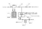
- FIG. 1 is a schematic view showing an example of an ALD apparatus used in the method for producing a thin film according to the present invention.
- FIG. 2 is a schematic view showing another example of the ALD apparatus used in the method for producing a thin film according to the present invention.
- FIG. 3 is a schematic view showing still another example of the ALD apparatus used in the method for producing a thin film according to the present invention.
- FIG. 4 is a schematic view showing still another example of the ALD apparatus used in the method for producing a thin film according to the present invention.
- the compound of the present invention is represented by the above general formula (1).
- the compound of the present invention is suitable as a precursor in a method for producing a thin film having a vaporization step such as the ALD method, which is a kind of CVD method.
- R 1 and R 2 each independently represent an alkyl group having 1 to 5 carbon atoms
- R 3 represents a hydrogen atom or an alkyl group having 1 to 5 carbon atoms
- M Represents a metal atom or a silicon atom
- n represents the valence of the atom represented by M.
- at least one hydrogen atom of R 1 to R 3 is replaced with a fluorine atom.
- alkyl group having 1 to 5 carbon atoms a methyl group, an ethyl group, a propyl group, an isopropyl group, a butyl group, an isobutyl group, a second butyl group, a third butyl group, a pentyl group, an isopentyl group, and a neopentyl group. And so on.
- At least one hydrogen atom existing in R 1 to R 3 is replaced with a fluorine atom.
- a fluorine atom Of all the hydrogen atoms present in R 1 to R 3 , preferably 1 to 9, more preferably 1 to 7, still more preferably 2 to 6, and even more preferably 3 to 6 hydrogen atoms. Is replaced by a fluorine atom.
- an amidinate compound in which three hydrogen atoms are replaced with fluorine atoms is included as the aziminate compound of the present invention.
- Trifluoromethyl group perfluoromethyl group
- difluoromethyl group mono as an alkyl group having 1 to 5 carbon atoms (hereinafter, also referred to as "fluorinated alkyl group”) in which at least one hydrogen is substituted with a fluorine atom.
- an alkyl fluoride group containing a trifluoromethyl (CF 3 ) group is preferable, and specifically, a trifluoromethyl group, a perfluoroethyl group, and 2,2,2-tri Fluoroethyl group, perfluoropropyl group, 3,3,3-trifluoropropyl group, 1,1,1-trifluoroisopropyl group, 1,1,1,3,3,3-hexafluoroisopropyl group, perfluoro Butyl group, 2,2,3,3,4,4,4-heptafluorobutyl group, 3,3,4,5,4-pentafluorobutyl group, 4,4,4-trifluorobutyl group, perfluoro Examples include a pentyl group, a 3,3,4,5,4,5,5-heptafluoropentyl group, a 4,4,5,5,5-pentafluoropentyl group, a 5,5,5-trifluoropenty
- the aziminate compound of the present invention preferably contains 3 fluorine atoms per compound (excluding dimers).
- the any one of R 1 ⁇ R 3, is preferably a fluorinated alkyl group containing a trifluoromethyl (CF 3) groups, any one of the specifically the R 1 ⁇ R 3, tri It is preferably a fluoromethyl group, a 2,2,2-trifluoroethyl group or a 1,1,1-trifluoroisopropyl group.
- M in the general formula (1) represents a metal atom or a silicon atom.
- the metal atom represented by M include a copper atom, a cobalt atom, a nickel atom, a manganese atom, a zinc atom, a tin atom, an yttrium atom, an indium atom or a titanium atom, and a gallium atom.
- R 1 to R 3 and M are appropriately selected according to the method for producing a thin film to be applied.
- R 1 to R 3 and M it is preferable to select R 1 to R 3 and M so that the compound has a large vapor pressure and a low melting point.
- R 1 is preferably an alkyl group having 1 to 5 carbon atoms (alkyl fluoride group) in which at least one hydrogen atom is substituted with a fluorine atom, and the carbon atom is preferable.
- Alkyl fluoride groups of numbers 1 to 3 are more preferred, trifluoromethyl groups, 2,2,2-trifluoroethyl groups or 1,1,1-trifluoroisopropyl groups are even more preferred, and 2,2,2-tri Fluoroethyl groups are most preferred.
- R 2 Since the thermal stability of the compound is high, as R 2 , an unsubstituted alkyl group having 1 to 5 carbon atoms is preferable, a branched alkyl group having 3 to 5 carbon atoms is more preferable, and an unsubstituted alkyl group is more preferable.
- the tertiary butyl group is most preferred.
- R 3 is preferably a hydrogen atom or a linear unsubstituted alkyl group having 1 to 5 carbon atoms, and a linear unsubstituted alkyl group having 1 to 3 carbon atoms is preferable. More preferably, a methyl group or an ethyl group is particularly preferable, and an ethyl group is most preferable.
- M Copper atom, cobalt atom, nickel atom, manganese atom, zinc atom, tin atom, yttrium atom, indium atom, titanium atom, gallium atom or silicon atom are preferable as M because high quality thin film can be produced with high productivity. , Cobalt atom or tin atom is more preferable. Further, since a high-quality thin film can be produced with high productivity, when M is a copper atom, the compound represented by the above general formula (1) is preferably a dimer compound, and M is a cobalt atom.
- the compound represented by the above general formula (1) is a monomer compound.
- the compound represented by the general formula (1) is preferably a dimer compound, and when n is 2 or more, the general formula (1)
- the compound represented by is preferably a monomeric compound.
- N in the above general formula (1) represents the valence of the atom represented by M.
- n is preferably 1 to 6, more preferably 1 to 4, further preferably 1 to 3, and most preferably 2.
- R 1 to R 3 can be arbitrarily selected depending on the solubility in the solvent used, the thin film forming reaction, and the like. ..
- the following compound No. 1 to No. 132 is mentioned.
- the following compound No. 1 to No. In 132 "Me” represents a methyl group, “Et” represents an ethyl group, “nPr” represents a normal propyl group, and “iPr” represents an isopropyl group.
- the method for producing the compound represented by the above general formula (1) is not particularly limited, and the compound is produced by applying a well-known reaction.
- an intermediate compound is obtained by reacting and purifying iron chloride, a nitrile compound having a corresponding structure, an alkyl halide compound having a corresponding structure, and a fluorine-containing amine compound having a corresponding structure under a dichloromethane solvent. .. Then, it is obtained by reacting the obtained intermediate compound with a chloride of the corresponding metal and alkyllithium under a tetrahydrofuran solvent, filtering the mixture, distilling off the solvent from the filtrate, and then distilling and purifying the mixture. be able to.
- the nitrile compound is represented by R 4- CN, and R 4 has a group corresponding to R 3 of the general formula (1).
- the alkyl halide compound is represented by R 5- X, R 5 has a group corresponding to R 2 of the general formula (1), and X represents halogen.
- the fluorine-containing amine compound is represented by R 6- NH 2 , and R 6 has a group corresponding to R 1 of the general formula (1).
- the raw material for forming a thin film of the present invention contains a compound represented by the above general formula (1) as a thin film precursor. Its form depends on the manufacturing process to which the thin film forming raw material is applied. For example, when producing a thin film containing only a metal atom or a silicon atom as a metal, the raw material for forming a thin film of the present invention does not contain a metal compound or a metalloid compound other than the compound represented by the above general formula (1).
- the raw material for forming a thin film of the present invention is a compound containing a desired metal in addition to the compound represented by the above general formula (1). And / or a compound containing a semimetal (hereinafter, may be referred to as "another precursor") may be contained.
- the raw material for forming a thin film of the present invention may further contain an organic solvent and / or a nucleophilic reagent, as will be described later.
- the raw material for thin film formation of the present invention is a raw material for chemical vapor deposition (hereinafter, "CVD"). It is also useful as a “raw material”).
- CVD chemical vapor deposition
- the raw material for forming a thin film of the present invention is particularly suitable for the ALD method.
- the raw material for thin film formation of the present invention is a raw material for chemical vapor deposition
- the form thereof is appropriately selected by a method such as a transportation supply method of the CVD method used.
- the CVD raw material is vaporized by heating and / or depressurizing in a container in which the raw material is stored (hereinafter, may be referred to as a “raw material container”) to obtain a raw material gas.
- a gas that introduces the raw material gas into a film forming chamber in which a substrate is installed hereinafter, may be referred to as a "deposition reaction part" together with a carrier gas such as argon, nitrogen, and helium that is used as needed.
- a liquid that transports a raw material for CVD in a liquid or solution state to a vaporization chamber vaporizes it by heating and / or depressurizing it in the vaporization chamber to obtain a raw material gas, and introduces the raw material gas into a film forming chamber.
- the compound itself represented by the above general formula (1) can be used as a CVD raw material.
- the compound itself represented by the general formula (1) or a solution obtained by dissolving the compound in an organic solvent can be used as a raw material for CVD.
- These CVD raw materials may further contain other precursors, nucleophiles and the like.
- a method of vaporizing and supplying the CVD raw material independently for each component (hereinafter, may be referred to as “single source method”) and a method of preliminarily preparing the multi-component raw material with a desired composition.
- a method of vaporizing and supplying the mixed mixed raw materials (hereinafter, also referred to as "cocktail sauce method”).
- the cocktail sauce method a mixture of the compound represented by the above general formula (1) and another precursor or a mixed solution obtained by dissolving the mixture in an organic solvent can be used as a raw material for CVD.
- This mixture or mixed solution may further contain a nucleophile or the like.
- organic solvent a well-known general organic solvent can be used without any particular limitation.
- organic solvent include acetate esters such as ethyl acetate, butyl acetate and methoxyethyl acetate; ethers such as tetrahydrofuran, tetrahydropyran, ethylene glycol dimethyl ether, diethylene glycol dimethyl ether, triethylene glycol dimethyl ether, dibutyl ether and dioxane; methyl.
- Ketones such as butyl ketone, methyl isobutyl ketone, ethyl butyl ketone, dipropyl ketone, diiso butyl ketone, methyl amyl ketone, cyclohexanone, methyl cyclohexanone; hexane, cyclohexane, methylcyclohexane, dimethylcyclohexane, ethylcyclohexane, heptane, octane, toluene, Hydrocarbons such as xylene; 1-cyanopropane, 1-cyanobutane, 1-cyanohexane, cyanocyclohexane, cyanobenzene, 1,3-dicyanopropane, 1,4-dicyanobutane, 1,6-dicyanohexane, 1, Hydrocarbons having a cyano group such as 4-dicyanocyclohexane and 1,4-
- the total amount of the precursor in the thin film forming raw material is preferably 0.01 mol / liter to 2.0 mol / liter. , 0.05 mol / liter to 1.0 mol / liter, more preferably.
- the total amount of the precursor is the above general formula (1) when the raw material for forming a thin film of the present invention does not contain a metal compound or a semi-metal compound other than the compound represented by the above general formula (1). It means the amount of the compound represented by, and the raw material for forming a thin film of the present invention contains a compound containing another metal in addition to the compound represented by the above general formula (1) and / or a compound containing a semi-metal (others). In the case of containing the precursor), it means the total amount of the compound represented by the above general formula (1) and other precursors.
- the other precursor used together with the compound represented by the above general formula (1) is not particularly limited, and is a well-known general precursor used as a raw material for CVD. Can be used.
- the other precursors described above include one or more selected from the group consisting of compounds used as organic ligands such as alcohol compounds, glycol compounds, ⁇ -diketone compounds, cyclopentadiene compounds, and organic amine compounds. , Compounds with silicon and metals.
- Precasa metal species include lithium, sodium, potassium, magnesium, calcium, samarium, barium, titanium, zirconium, hafnium, vanadium, tantalum, chromium, molybdenum, tungsten, manganese, iron, cobalt, rhodium, iridium, nickel and palladium.
- Examples of the alcohol compound used as the organic ligand of the above-mentioned precursor include methanol, ethanol, propanol, isopropyl alcohol, butanol, secondary butyl alcohol, isobutyl alcohol, tertiary butyl alcohol, pentyl alcohol, isopentyl alcohol, and the like.
- Alcohols such as 3pentyl alcohols; 2-methoxyethanol, 2-ethoxyethanol, 2-butoxyethanol, 2- (2-methoxyethoxy) ethanol, 2-methoxy-1-methylethanol, 2-methoxy-1,1 -Dimethylethanol, 2-ethoxy-1,1-dimethylethanol, 2-isopropoxy-1,1-dimethylethanol, 2-butoxy-1,1-dimethylethanol, 2- (2-methoxyethoxy) -1,1 Ether alcohols such as -dimethylethanol, 2-propoxy-1,1-diethylethanol, 2-s-butoxy-1,1-diethylethanol, 3-methoxy-1,1-dimethylpropanol; dimethylaminoethanol, ethylmethyl Aminoethanol, diethylaminoethanol, dimethylamino-2-pentanol, ethylmethylamino-2-pentanol, dimethylamino-2-methyl-2-pentanol, ethylmethyla
- glycol compound used as the organic ligand of the other precursors described above examples include 1,2-ethanediol, 1,2-propanediol, 1,3-propanediol, 2,4-hexanediol, and 2,2-.
- Examples of the ⁇ -diketone compound used as the organic ligand of the above-mentioned precursor include acetylacetone, hexane-2,4-dione, 5-methylhexane-2,4-dione, heptane-2,4-dione, 2 -Methylheptan-3,5-dione, 5-methylheptane-2,4-dione, 6-methylheptan-2,4-dione, 2,2-dimethylheptan-3,5-dione, 2,6-dimethyl Heptan-3,5-dione, 2,2,6-trimethylheptan-3,5-dione, 2,2,6,6-tetramethylheptan-3,5-dione, octane-2,4-dione, 2 , 2,6-trimethyloctane-3,5-dione, 2,6-dimethyloctane-3,5-dione, 2,9-dimethylnonane-4
- cyclopentadiene compound used as the organic ligand of the other precursors described above examples include cyclopentadiene, methylcyclopentadiene, ethylcyclopentadiene, propylcyclopentadiene, isopropylcyclopentadiene, butylcyclopentadiene, second butylcyclopentadiene, and isobutylcyclo.
- examples thereof include pentadiene, third butylcyclopentadiene, dimethylcyclopentadiene, and tetramethylcyclopentadiene.
- Examples of the organic amine compound used as the organic ligand of the above-mentioned precursor include methylamine, ethylamine, propylamine, isopropylamine, butylamine, secondary butylamine, tertiary butylamine, isobutylamine, dimethylamine, diethylamine and dipropyl. Examples thereof include amines, diisopropylamines, ethylmethylamines, propylmethylamines and isopropylmethylamines.
- the other precursors described above are known in the art, and their manufacturing methods are also known.
- the above-mentioned inorganic salt of the metal or its hydrate is reacted with the alkali metal alkoxide of the alcohol compound.
- the inorganic salt of the metal or its hydrate include metal halides and nitrates
- examples of the alkali metal alkoxide include sodium alkoxide, lithium alkoxide, potassium alkoxide and the like.
- the single source method it is preferable to use a compound whose behavior of thermal decomposition and / or oxidative decomposition is similar to that of the compound represented by the above general formula (1) as the other precursor described above.
- the cocktail sauce method as the other precursors described above, in addition to the behavior of thermal decomposition and / or oxidative decomposition being similar to that of the compound represented by the above general formula (1), a chemical reaction during mixing, etc. Therefore, it is preferable to use a compound that does not cause a change that impairs the desired properties as a precursor.
- the raw material for thin film formation of the present invention may contain a nucleophile, if necessary, in order to impart stability to the compound represented by the above general formula (1) and other precursors.
- the nucleophilic reagent include ethylene glycol ethers such as glyme, jigglime, triglime, and tetraglime, 18-crown-6, dicyclohexyl-18-crown-6, 24-crown-8, and dicyclohexyl-24-crown-8.
- Dibenzo-24 Crown-8 and other crown ethers ethylenediamine, N, N'-tetramethylethylenediamine, diethylenetriamine, triethylenetetramine, tetraethylenepentamine, pentaethylenehexamine, 1,1,4,7,7- Polyamines such as pentamethyldiethylenetriamine, 1,1,4,7,10,10-hexamethyltriethylenetetrahydrofuran, triethoxytriethyleneamine, cyclic polyamines such as cyclolam and cyclone, pyridine, pyrrolidine, piperidine, morpholine, N.
- -Methylpyrrolidin N-methylpiperidin, N-methylmorpholine, tetrahydrofuran, tetrahydropyran, 1,4-dioxane, oxazole, thiazole, oxathiolane and other heterocyclic compounds, methyl acetoacetate, ethyl acetoacetate, acetoacetic acid-2- Examples thereof include ⁇ -ketoesters such as methoxyethyl or ⁇ -diketones such as acetylacetone, 2,4-hexanedione, 2,4-heptandione, 3,5-heptandione and dipivaloylmethane.
- the amount of these nucleophiles used is preferably 0.1 mol to 10 mol, more preferably 1 to 4 mol, based on 1 mol of the total amount of the precursor.
- the raw material for thin film formation of the present invention should contain as little as possible impurity metal elements other than the constituents thereof, impurity halogens such as impurity chlorine, and impurity organics.
- the impurity metal element content is preferably 100 ppb or less for each element, more preferably 10 ppb or less, and the total amount is preferably 1 ppm or less, more preferably 100 ppb or less.
- the impurity halogen content is preferably 100 ppm or less, more preferably 10 ppm or less, and most preferably 1 ppm or less.
- the total amount of the impurity organic content is preferably 500 ppm or less, more preferably 50 ppm or less, and most preferably 10 ppm or less.
- Moisture causes particles to be generated in the raw materials for chemical vapor deposition and particles to be generated during thin film formation. Therefore, for precursors, organic solvents and nucleophiles, as much water as possible before use. It is preferable to remove.
- the water content of each of the precursor, the organic solvent and the nucleophile is preferably 10 ppm or less, and more preferably 1 ppm or less.
- the raw material for forming a thin film of the present invention preferably contains as little particles as possible in order to reduce or prevent particle contamination of the formed thin film.
- the number of particles larger than 0.3 ⁇ m is preferably 100 or less in 1 mL of the liquid phase, and is larger than 0.2 ⁇ m.
- the number of particles is more preferably 1000 or less in 1 mL of the liquid phase, and most preferably the number of particles larger than 0.2 ⁇ m is 100 or less in 1 mL of the liquid phase.
- a method for producing a thin film using the raw material for forming a thin film of the present invention will be described.
- a raw material gas obtained by vaporizing the raw material for forming a thin film of the present invention and a reactive gas used as needed are introduced into a film forming chamber (treatment atmosphere) in which a substrate is installed.
- the precursor in the raw material gas is decomposed and / or chemically reacted on the substrate to grow and deposit a thin film containing a metal atom or a silicon atom on the substrate surface.
- the method of transporting and supplying the raw material, the method of depositing, the manufacturing conditions, the manufacturing equipment, and the like are not particularly limited, and well-known general conditions and methods can be used.
- Examples of the reactive gas used as necessary include oxidizing gases such as oxygen, ozone and water vapor, hydrocarbon compounds such as methane and ethane, and reducing gases such as hydrogen, carbon monoxide and organic metal compounds. , Organic amine compounds such as monoalkylamines, dialkylamines, trialkylamines and alkylenediamines, and nitrided gases such as hydrazine and ammonia. These reactive gases may be used alone or in combination of two or more.
- the compound represented by the general formula (1) has a property of reacting well with an oxidizing gas or a reducing gas, and has a property of reacting particularly well with water vapor or hydrogen. Therefore, as the reactive gas, it is preferable to use an oxidizing gas or a reducing gas, and it is particularly preferable to use water vapor or hydrogen.
- the above-mentioned transportation supply method the above-mentioned gas transportation method, liquid transportation method, single source method, cocktail sauce method and the like can be mentioned.
- the above deposition methods include thermal CVD in which a raw material gas or a raw material gas and a reactive gas are reacted only by heat to deposit a thin film, plasma CVD using heat and plasma, optical CVD using heat and light, and heat. , Photoplasma CVD using light and plasma, ALD in which the deposition reaction of CVD is divided into elementary processes and the deposition is carried out stepwise at the molecular level.
- Examples of the material of the substrate include silicon; ceramics such as silicon nitride, titanium nitride, tantalum nitride, titanium oxide, titanium nitride, ruthenium oxide, zirconium oxide, hafnium oxide and lanthanum oxide; and glass; metals such as metallic cobalt. Be done.
- Examples of the shape of the substrate include plate-like, spherical, fibrous, and scaly shapes.
- the surface of the substrate may be flat or may have a three-dimensional structure such as a trench structure.
- reaction temperature base temperature
- reaction pressure deposition rate and the like.
- the reaction temperature is preferably room temperature to 500 ° C, more preferably 100 ° C to 300 ° C.
- the reaction pressure is preferably 10 Pa to atmospheric pressure in the case of thermal CVD or optical CVD, and preferably 10 Pa to 2,000 Pa in the case of using plasma.
- the deposition rate can be controlled by the supply conditions (vaporization temperature, vaporization pressure), reaction temperature, and reaction pressure of the raw materials. If the deposition rate is high, the characteristics of the obtained thin film may deteriorate, and if it is low, problems may occur in productivity. Therefore, 0.01 nm / min to 100 nm / min is preferable, and 1 nm / min to 50 nm / min. Is more preferable. Further, in the case of the ALD method, the number of cycles is controlled so that a desired film thickness can be obtained.
- the step of vaporizing the raw material for forming a thin film into a raw material gas may be performed in a raw material container or in a vaporization chamber.
- the raw material for forming a thin film of the present invention is preferably evaporated at 0 ° C. to 150 ° C.
- the pressure in the raw material container and the pressure in the vaporization chamber are both preferably 1 Pa to 10,000 Pa.
- the thin film manufacturing method of the present invention employs the ALD method, and the raw material for thin film formation is vaporized into a raw material gas by the above-mentioned transportation and supply method, and the raw material gas is introduced into the film forming chamber.
- a precursor thin film forming step of forming a precursor thin film on the surface of the substrate by the compound in the raw material gas an exhaust step of exhausting an unreacted compound gas, and a chemical reaction of the precursor thin film with a reactive gas. It may have a metal-containing thin film forming step of forming a metal-containing thin film on the surface of the substrate.
- each step of the above ALD method will be described in detail by taking the case of forming a metal thin film as an example.
- the raw material introduction step described above is performed.
- the preferable temperature and pressure when the raw material for thin film formation is used as the raw material gas are the same as those described in the method for producing a thin film by the CVD method.
- a precursor thin film is formed on the surface of the substrate by contacting the raw material gas introduced into the film forming chamber with the surface of the substrate (precursor thin film forming step). At this time, the substrate may be heated or the film forming chamber may be heated to apply heat.
- the precursor thin film formed in this step is a thin film formed from the compound represented by the general formula (1), or a part of the compound represented by the general formula (1) is decomposed and / or. Alternatively, it is a thin film produced by reaction and has a composition different from that of the target metal thin film.
- the substrate temperature at which this step is performed is preferably room temperature to 500 ° C, more preferably 100 ° C to 300 ° C.
- the pressure of the system (inside the film forming chamber) when this step is performed is preferably 1 Pa to 10,000 Pa, more preferably 10 Pa to 1,000 Pa.
- unreacted compound gas and by-produced gas are exhausted from the film formation chamber (exhaust process).
- the unreacted compound gas or by-produced gas is completely exhausted from the film forming chamber, but it is not always necessary to completely exhaust the gas.
- the exhaust method include a method of purging the inside of the system with an inert gas such as nitrogen, helium, and argon, a method of exhausting by depressurizing the inside of the system, and a method of combining these.
- the degree of pressure reduction is preferably 0.01 Pa to 300 Pa, more preferably 0.01 Pa to 100 Pa.
- a reducing gas is introduced as a reactive gas into the film forming chamber, and the precursor thin film obtained in the previous precursor thin film forming step is subjected to the action of the reducing gas or the action of the reducing gas and heat to form a metal thin film.
- Metal-containing thin film forming step The temperature at which heat is applied in this step is preferably room temperature to 500 ° C, more preferably 100 to 300 ° C.
- the pressure of the system (inside the film forming chamber) when this step is performed is preferably 1 Pa to 10,000 Pa, more preferably 10 Pa to 1,000 Pa. Since the compound represented by the general formula (1) has good reactivity with the reducing gas, a high-quality metal thin film having a low residual carbon content can be obtained.
- thin film deposition by a series of operations including the above-mentioned raw material introduction step, precursor thin film forming step, exhaust step and metal-containing thin film forming step is performed.
- the cycle may be repeated a plurality of times until a thin film having a required film thickness is obtained.
- energy such as plasma, light, or voltage may be applied, or a catalyst may be used.
- the timing of applying the energy and the timing of using the catalyst are not particularly limited, and are, for example, in the compound gas introduction in the raw material introduction step, the heating in the precursor thin film forming step or the metal-containing thin film forming step, and the exhaust step. It may be at the time of exhausting in the system, at the time of introducing the reducing gas in the metal-containing thin film forming step, or during each of the above steps.
- annealing treatment may be performed in an inert atmosphere, an oxidizing atmosphere or a reducing atmosphere in order to obtain better electrical characteristics. If embedding is required, a reflow process may be provided.
- the temperature in this case is 200 ° C. to 1,000 ° C., preferably 250 ° C. to 500 ° C.
- a well-known ALD device can be used in the method for producing a thin film of the present invention.
- the ALD device include a device capable of bubbling and supplying a precursor as shown in FIGS. 1 and 3, and a device having a vaporization chamber as shown in FIGS. 2 and 4. Further, as shown in FIGS. 3 and 4, an apparatus capable of performing plasma treatment on the reactive gas can be mentioned.
- the device is not limited to the single-wafer type device provided with the film forming chamber (hereinafter referred to as “deposition reaction part”) as shown in FIGS. 1 to 4, and a device capable of simultaneously processing a large number of sheets using a batch furnace should be used. You can also. These can also be used as a CVD apparatus.
- the thin film produced by using the raw material for forming a thin film of the present invention is of a desired type such as metal, oxide ceramics, nitride ceramics, glass, etc. by appropriately selecting other precursors, reactive gases and production conditions. It can be a thin film.
- the thin film is known to exhibit electrical characteristics, optical characteristics, and the like, and is applied to various applications.
- a metal thin film, a metal oxide thin film, a gold nitride thin film, an alloy, a metal-containing composite oxide thin film, and the like can be mentioned.
- These thin films are widely used, for example, in the production of electrode materials for memory elements represented by DRAM elements, resistance films, diamagnetic films used for recording layers of hard disks, catalyst materials for polymer electrolyte fuel cells, and the like. ing.
- Example 1 Compound No. Production of 19 Cobalt chloride (6.046 mol) and tetrahydrofuran (32.9 g) were charged into a 300 mL three-necked flask and stirred at room temperature. A solution prepared by adding 18.5 g (0.094 mol) of Intermediate Compound 1, 59.4 g of tetrahydrofuran, and 60 ml (0.094 mol) of nBuLi was added dropwise thereto under ice-cooling, and after the addition, the mixture was returned to room temperature and stirred for 17 hours. , Filtered.
- Example 2 Compound No. Production of No. 20 13.1 g (0.101 mol) of cobalt chloride and 70.3 g of tetrahydrofuran were placed in a 500 mL three-necked flask and stirred at room temperature. A solution prepared with 42.9 g (0.204 mol) of the intermediate compound 2, tetrahydrofuran 63.3 g, and nBuLi 130 ml (0.204 mol) was added dropwise thereto under ice-cooling, and the mixture was returned to room temperature and stirred for 17 hours. , Filtered.
- Example 3 Compound No. Production of 68 33.8 g (0.077 mol) of bis (trimethylsilylamide) tin and 89.2 g of normal hexane were placed in a 300 mL three-necked flask and stirred at room temperature. 32.5 g (0.154 mol) of the intermediate compound 2 was added dropwise thereto under ice-cooling, and after the addition, the mixture was returned to room temperature, stirred for 17 hours, and filtered. The solvent was removed from the obtained filtrate, and the residue was purified at a bath temperature of 135 ° C. and a pressure of 45 Pa. I got 68. The yield was 35.4 g and the yield was 86%.
- the amidinate compound and its dimer compound of the present invention are compounds having a higher vapor pressure than the conventionally known amidinate compound and its dimer compound.
- compound No. 19 and No. It was found that No. 20 was a compound having a melting point lower than that of Comparative Compound 1 by 45 ° C. or more.
- Compound No. 20 was found to be a liquid at 20 ° C., particularly a compound having a low melting point.
- compound No. 68 was found to be a compound having a melting point lower than that of Comparative Compound 2 by 15 ° C. or more.
- the carbon content in the metal thin film obtained by the ALD method is 5 atm% or more in Comparative Examples 1 and 2, whereas it is less than the detection limit of 0.1 atm% in Examples 4 to 6. That is, it was shown that a high-quality metal thin film can be obtained by using the amidinate compound of the present invention and its dimer compound. Further, the film thickness of the obtained thin film is 3.5 nm or less in Comparative Examples 1 and 2, whereas it is 6.5 nm or more in Examples 4 to 6, and the amidinate compound of the present invention and its dimer compound thereof. A metal thin film was obtained with high productivity.
- compound No. No. 20 is a liquid at 20 ° C., and when used as a raw material for chemical vapor deposition, a metal thin film can be obtained with particularly high productivity. Therefore, it is particularly excellent as a raw material for chemical vapor deposition. Shown.
Landscapes
- Chemical & Material Sciences (AREA)
- Organic Chemistry (AREA)
- General Chemical & Material Sciences (AREA)
- Chemical Kinetics & Catalysis (AREA)
- Engineering & Computer Science (AREA)
- Materials Engineering (AREA)
- Mechanical Engineering (AREA)
- Metallurgy (AREA)
- Inorganic Chemistry (AREA)
- Chemical Vapour Deposition (AREA)
- Organic Low-Molecular-Weight Compounds And Preparation Thereof (AREA)
Priority Applications (6)
| Application Number | Priority Date | Filing Date | Title |
|---|---|---|---|
| EP21783689.9A EP4134372A4 (en) | 2020-04-10 | 2021-03-31 | AMIDINATE COMPOUND, DIMER COMPOUND THEREOF, RAW MATERIAL FOR FORMING THIN FILM, AND METHOD FOR PRODUCING THIN FILM |
| CN202180027605.8A CN115380038A (zh) | 2020-04-10 | 2021-03-31 | 脒基化合物、其二聚体化合物、薄膜形成用原料以及薄膜的制造方法 |
| KR1020227038495A KR20220167299A (ko) | 2020-04-10 | 2021-03-31 | 아미디네이트 화합물, 그 2 량체 화합물, 박막 형성용 원료 및 박막의 제조 방법 |
| IL297232A IL297232B1 (en) | 2020-04-10 | 2021-03-31 | An amidinate compound, a dimer compound thereof, a raw material for forming a thin layer, and a method for producing a thin layer |
| JP2022514432A JP7787806B2 (ja) | 2020-04-10 | 2021-03-31 | アミジナート化合物、その二量体化合物、薄膜形成用原料及び薄膜の製造方法 |
| US17/917,671 US12275748B2 (en) | 2020-04-10 | 2021-03-31 | Amidinate compound, dimer compound thereof, thin-film forming raw material, and method of producing thin film |
Applications Claiming Priority (2)
| Application Number | Priority Date | Filing Date | Title |
|---|---|---|---|
| JP2020-070708 | 2020-04-10 | ||
| JP2020070708 | 2020-04-10 |
Publications (1)
| Publication Number | Publication Date |
|---|---|
| WO2021205958A1 true WO2021205958A1 (ja) | 2021-10-14 |
Family
ID=78023767
Family Applications (1)
| Application Number | Title | Priority Date | Filing Date |
|---|---|---|---|
| PCT/JP2021/013898 Ceased WO2021205958A1 (ja) | 2020-04-10 | 2021-03-31 | アミジナート化合物、その二量体化合物、薄膜形成用原料及び薄膜の製造方法 |
Country Status (8)
| Country | Link |
|---|---|
| US (1) | US12275748B2 (https=) |
| EP (1) | EP4134372A4 (https=) |
| JP (1) | JP7787806B2 (https=) |
| KR (1) | KR20220167299A (https=) |
| CN (1) | CN115380038A (https=) |
| IL (1) | IL297232B1 (https=) |
| TW (1) | TWI873328B (https=) |
| WO (1) | WO2021205958A1 (https=) |
Families Citing this family (2)
| Publication number | Priority date | Publication date | Assignee | Title |
|---|---|---|---|---|
| US12371778B2 (en) * | 2021-07-12 | 2025-07-29 | Adeka Corporation | Cobalt compound, thin-film forming raw material, thin-film, and method of producing thin-film |
| WO2025132279A1 (en) | 2023-12-18 | 2025-06-26 | Merck Patent Gmbh | Group 13 metal compounds for ald applications |
Citations (4)
| Publication number | Priority date | Publication date | Assignee | Title |
|---|---|---|---|---|
| WO2006012052A2 (en) * | 2004-06-25 | 2006-02-02 | Arkema, Inc. | Amidinate ligand containing chemical vapor deposition precursors |
| JP2006511716A (ja) | 2002-11-15 | 2006-04-06 | プレジデント・アンド・フェロウズ・オブ・ハーバード・カレッジ | 金属アミジナートを用いる原子層の析出 |
| JP2009542654A (ja) * | 2006-06-28 | 2009-12-03 | プレジデント アンド フェロウズ オブ ハーバード カレッジ | 金属(iv)テトラ−アミジネート化合物ならびに蒸着においての使用 |
| WO2018088079A1 (ja) | 2016-11-08 | 2018-05-17 | 株式会社Adeka | 化合物、薄膜形成用原料、薄膜の製造方法及びアミジン化合物 |
-
2021
- 2021-03-31 WO PCT/JP2021/013898 patent/WO2021205958A1/ja not_active Ceased
- 2021-03-31 CN CN202180027605.8A patent/CN115380038A/zh active Pending
- 2021-03-31 EP EP21783689.9A patent/EP4134372A4/en active Pending
- 2021-03-31 JP JP2022514432A patent/JP7787806B2/ja active Active
- 2021-03-31 US US17/917,671 patent/US12275748B2/en active Active
- 2021-03-31 IL IL297232A patent/IL297232B1/en unknown
- 2021-03-31 KR KR1020227038495A patent/KR20220167299A/ko active Pending
- 2021-04-08 TW TW110112649A patent/TWI873328B/zh active
Patent Citations (5)
| Publication number | Priority date | Publication date | Assignee | Title |
|---|---|---|---|---|
| JP2006511716A (ja) | 2002-11-15 | 2006-04-06 | プレジデント・アンド・フェロウズ・オブ・ハーバード・カレッジ | 金属アミジナートを用いる原子層の析出 |
| JP2010156058A (ja) | 2002-11-15 | 2010-07-15 | President & Fellows Of Harvard College | 金属アミジナートを用いる原子層の析出 |
| WO2006012052A2 (en) * | 2004-06-25 | 2006-02-02 | Arkema, Inc. | Amidinate ligand containing chemical vapor deposition precursors |
| JP2009542654A (ja) * | 2006-06-28 | 2009-12-03 | プレジデント アンド フェロウズ オブ ハーバード カレッジ | 金属(iv)テトラ−アミジネート化合物ならびに蒸着においての使用 |
| WO2018088079A1 (ja) | 2016-11-08 | 2018-05-17 | 株式会社Adeka | 化合物、薄膜形成用原料、薄膜の製造方法及びアミジン化合物 |
Non-Patent Citations (2)
| Title |
|---|
| LI JIAYE, WU JINPING, ZHOU CHENGGANG, HAN BO, LEI XINJIAN, GORDON ROY, CHENG HANSONG: "On the relative stability of cobalt- and nickel-based amidinate complexes against β-migration", INTERNATIONAL JOURNAL OF QUANTUM CHEMISTRY, WILEY, NEW YORK, NY, US, vol. 109, no. 4, 15 March 2009 (2009-03-15), US , pages 756 - 763, XP055865355, ISSN: 0020-7608, DOI: 10.1002/qua.21880 * |
| See also references of EP4134372A4 |
Also Published As
| Publication number | Publication date |
|---|---|
| US12275748B2 (en) | 2025-04-15 |
| CN115380038A (zh) | 2022-11-22 |
| JP7787806B2 (ja) | 2025-12-17 |
| US20230151041A1 (en) | 2023-05-18 |
| IL297232A (en) | 2022-12-01 |
| EP4134372A1 (en) | 2023-02-15 |
| TW202144376A (zh) | 2021-12-01 |
| KR20220167299A (ko) | 2022-12-20 |
| EP4134372A4 (en) | 2024-07-17 |
| JPWO2021205958A1 (https=) | 2021-10-14 |
| TWI873328B (zh) | 2025-02-21 |
| IL297232B1 (en) | 2026-04-01 |
Similar Documents
| Publication | Publication Date | Title |
|---|---|---|
| JPWO2019203035A1 (ja) | 原子層堆積法用薄膜形成用原料及び薄膜の製造方法 | |
| WO2014077089A1 (ja) | 金属アルコキシド化合物、薄膜形成用原料、薄膜の製造方法及びアルコール化合物 | |
| JP5690684B2 (ja) | アルコキシド化合物 | |
| JPWO2020071175A1 (ja) | 原子層堆積法用薄膜形成用原料、薄膜形成用原料、薄膜の製造方法および化合物 | |
| WO2019097768A1 (ja) | ルテニウム化合物、薄膜形成用原料及び薄膜の製造方法 | |
| WO2021200218A1 (ja) | 原子層堆積法用薄膜形成用原料及び薄膜の製造方法 | |
| JP7787806B2 (ja) | アミジナート化合物、その二量体化合物、薄膜形成用原料及び薄膜の製造方法 | |
| WO2021085210A1 (ja) | 新規化合物、該化合物を含有する薄膜形成用原料及び薄膜の製造方法 | |
| WO2021075397A1 (ja) | 新規スズ化合物、該化合物を含有する薄膜形成用原料、該薄膜形成用原料を用いて形成される薄膜、該薄膜を製造するために該化合物をプリカーサとして用いる方法、及び該薄膜の製造方法 | |
| JP7669367B2 (ja) | アルコキシド化合物、薄膜形成用原料及び薄膜の製造方法 | |
| WO2021200219A1 (ja) | 亜鉛化合物、薄膜形成用原料、薄膜及びその製造方法 | |
| WO2018088079A1 (ja) | 化合物、薄膜形成用原料、薄膜の製造方法及びアミジン化合物 | |
| WO2023054066A1 (ja) | 薄膜形成用原料、薄膜の製造方法、薄膜及びモリブデン化合物 | |
| JP7573514B2 (ja) | 薄膜形成用原料、薄膜の製造方法及び新規なスカンジウム化合物 | |
| WO2021106652A1 (ja) | 化合物、薄膜形成用原料及び薄膜の製造方法 | |
| WO2018042871A1 (ja) | ジアザジエニル化合物、薄膜形成用原料及び薄膜の製造方法 | |
| WO2021054160A1 (ja) | 原子層堆積法のための薄膜形成原料及びそれを用いた亜鉛含有薄膜の製造方法 | |
| TWI922746B (zh) | 薄膜形成用原料、薄膜之製造方法、薄膜及鉬化合物 | |
| JP7701969B2 (ja) | スズ化合物、薄膜形成用原料、薄膜、薄膜の製造方法及びハロゲン化合物 | |
| KR102946463B1 (ko) | 원자층 퇴적법용 박막 형성 원료 및 박막의 제조 방법 | |
| KR102859536B1 (ko) | 루테늄 화합물, 박막 형성용 원료 및 박막의 제조 방법 | |
| WO2023276716A1 (ja) | 薄膜形成用原料、薄膜及び薄膜の製造方法 | |
| WO2023286589A1 (ja) | コバルト化合物、薄膜形成用原料、薄膜及び薄膜の製造方法 | |
| WO2023282104A1 (ja) | 化合物、薄膜形成用原料、薄膜及び薄膜の製造方法 | |
| KR20230117368A (ko) | 인듐 화합물, 박막 형성용 원료, 박막 및 그 제조 방법 |
Legal Events
| Date | Code | Title | Description |
|---|---|---|---|
| 121 | Ep: the epo has been informed by wipo that ep was designated in this application |
Ref document number: 21783689 Country of ref document: EP Kind code of ref document: A1 |
|
| ENP | Entry into the national phase |
Ref document number: 2022514432 Country of ref document: JP Kind code of ref document: A |
|
| ENP | Entry into the national phase |
Ref document number: 20227038495 Country of ref document: KR Kind code of ref document: A |
|
| ENP | Entry into the national phase |
Ref document number: 2021783689 Country of ref document: EP Effective date: 20221110 |
|
| NENP | Non-entry into the national phase |
Ref country code: DE |
|
| WWG | Wipo information: grant in national office |
Ref document number: 17917671 Country of ref document: US |