WO2021193416A1 - 光学積層体および物品 - Google Patents
光学積層体および物品 Download PDFInfo
- Publication number
- WO2021193416A1 WO2021193416A1 PCT/JP2021/011337 JP2021011337W WO2021193416A1 WO 2021193416 A1 WO2021193416 A1 WO 2021193416A1 JP 2021011337 W JP2021011337 W JP 2021011337W WO 2021193416 A1 WO2021193416 A1 WO 2021193416A1
- Authority
- WO
- WIPO (PCT)
- Prior art keywords
- value
- optical laminate
- incident
- light
- layer
- Prior art date
Links
- 230000003287 optical effect Effects 0.000 title claims abstract description 171
- 239000000463 material Substances 0.000 claims abstract description 135
- 230000003373 anti-fouling effect Effects 0.000 claims description 26
- 238000000576 coating method Methods 0.000 claims description 26
- 239000011248 coating agent Substances 0.000 claims description 21
- 150000001875 compounds Chemical class 0.000 claims description 9
- YCKRFDGAMUMZLT-UHFFFAOYSA-N Fluorine atom Chemical compound [F] YCKRFDGAMUMZLT-UHFFFAOYSA-N 0.000 claims description 5
- 229910052731 fluorine Inorganic materials 0.000 claims description 5
- 239000011737 fluorine Substances 0.000 claims description 5
- 230000003667 anti-reflective effect Effects 0.000 abstract description 4
- 239000010410 layer Substances 0.000 description 190
- 230000000052 comparative effect Effects 0.000 description 40
- 239000010408 film Substances 0.000 description 37
- 229920005989 resin Polymers 0.000 description 34
- 239000011347 resin Substances 0.000 description 34
- 238000000034 method Methods 0.000 description 19
- 238000004519 manufacturing process Methods 0.000 description 15
- 239000007788 liquid Substances 0.000 description 12
- 239000000758 substrate Substances 0.000 description 10
- 238000012360 testing method Methods 0.000 description 10
- 239000002904 solvent Substances 0.000 description 9
- 229920002284 Cellulose triacetate Polymers 0.000 description 7
- NNLVGZFZQQXQNW-ADJNRHBOSA-N [(2r,3r,4s,5r,6s)-4,5-diacetyloxy-3-[(2s,3r,4s,5r,6r)-3,4,5-triacetyloxy-6-(acetyloxymethyl)oxan-2-yl]oxy-6-[(2r,3r,4s,5r,6s)-4,5,6-triacetyloxy-2-(acetyloxymethyl)oxan-3-yl]oxyoxan-2-yl]methyl acetate Chemical compound O([C@@H]1O[C@@H]([C@H]([C@H](OC(C)=O)[C@H]1OC(C)=O)O[C@H]1[C@@H]([C@@H](OC(C)=O)[C@H](OC(C)=O)[C@@H](COC(C)=O)O1)OC(C)=O)COC(=O)C)[C@@H]1[C@@H](COC(C)=O)O[C@@H](OC(C)=O)[C@H](OC(C)=O)[C@H]1OC(C)=O NNLVGZFZQQXQNW-ADJNRHBOSA-N 0.000 description 7
- 239000011230 binding agent Substances 0.000 description 7
- NIXOWILDQLNWCW-UHFFFAOYSA-M Acrylate Chemical compound [O-]C(=O)C=C NIXOWILDQLNWCW-UHFFFAOYSA-M 0.000 description 6
- 230000005865 ionizing radiation Effects 0.000 description 6
- 239000002245 particle Substances 0.000 description 6
- 238000004544 sputter deposition Methods 0.000 description 6
- VYPSYNLAJGMNEJ-UHFFFAOYSA-N Silicium dioxide Chemical compound O=[Si]=O VYPSYNLAJGMNEJ-UHFFFAOYSA-N 0.000 description 5
- 229910000831 Steel Inorganic materials 0.000 description 5
- 239000000945 filler Substances 0.000 description 5
- 239000010959 steel Substances 0.000 description 5
- 238000007740 vapor deposition Methods 0.000 description 5
- 210000002268 wool Anatomy 0.000 description 5
- PPBRXRYQALVLMV-UHFFFAOYSA-N Styrene Chemical compound C=CC1=CC=CC=C1 PPBRXRYQALVLMV-UHFFFAOYSA-N 0.000 description 4
- XLOMVQKBTHCTTD-UHFFFAOYSA-N Zinc monoxide Chemical compound [Zn]=O XLOMVQKBTHCTTD-UHFFFAOYSA-N 0.000 description 4
- LJCFOYOSGPHIOO-UHFFFAOYSA-N antimony pentoxide Chemical compound O=[Sb](=O)O[Sb](=O)=O LJCFOYOSGPHIOO-UHFFFAOYSA-N 0.000 description 4
- 239000003086 colorant Substances 0.000 description 4
- 238000004040 coloring Methods 0.000 description 4
- 238000011156 evaluation Methods 0.000 description 4
- 239000003999 initiator Substances 0.000 description 4
- 239000000203 mixture Substances 0.000 description 4
- MYWOJODOMFBVCB-UHFFFAOYSA-N 1,2,6-trimethylphenanthrene Chemical compound CC1=CC=C2C3=CC(C)=CC=C3C=CC2=C1C MYWOJODOMFBVCB-UHFFFAOYSA-N 0.000 description 3
- 229920000178 Acrylic resin Polymers 0.000 description 3
- 239000004925 Acrylic resin Substances 0.000 description 3
- KFZMGEQAYNKOFK-UHFFFAOYSA-N Isopropanol Chemical compound CC(C)O KFZMGEQAYNKOFK-UHFFFAOYSA-N 0.000 description 3
- 241000428199 Mustelinae Species 0.000 description 3
- 229910004298 SiO 2 Inorganic materials 0.000 description 3
- MPIAGWXWVAHQBB-UHFFFAOYSA-N [3-prop-2-enoyloxy-2-[[3-prop-2-enoyloxy-2,2-bis(prop-2-enoyloxymethyl)propoxy]methyl]-2-(prop-2-enoyloxymethyl)propyl] prop-2-enoate Chemical compound C=CC(=O)OCC(COC(=O)C=C)(COC(=O)C=C)COCC(COC(=O)C=C)(COC(=O)C=C)COC(=O)C=C MPIAGWXWVAHQBB-UHFFFAOYSA-N 0.000 description 3
- 239000003795 chemical substances by application Substances 0.000 description 3
- 238000004140 cleaning Methods 0.000 description 3
- 125000004386 diacrylate group Chemical group 0.000 description 3
- 238000010586 diagram Methods 0.000 description 3
- 238000001035 drying Methods 0.000 description 3
- 239000010419 fine particle Substances 0.000 description 3
- 239000007789 gas Substances 0.000 description 3
- 230000001678 irradiating effect Effects 0.000 description 3
- QSHDDOUJBYECFT-UHFFFAOYSA-N mercury Chemical compound [Hg] QSHDDOUJBYECFT-UHFFFAOYSA-N 0.000 description 3
- 229910052753 mercury Inorganic materials 0.000 description 3
- 239000012788 optical film Substances 0.000 description 3
- 229920006255 plastic film Polymers 0.000 description 3
- 239000002985 plastic film Substances 0.000 description 3
- 229920005668 polycarbonate resin Polymers 0.000 description 3
- 239000004431 polycarbonate resin Substances 0.000 description 3
- 229920001225 polyester resin Polymers 0.000 description 3
- 239000004645 polyester resin Substances 0.000 description 3
- 229920005672 polyolefin resin Polymers 0.000 description 3
- 239000000126 substance Substances 0.000 description 3
- 238000004381 surface treatment Methods 0.000 description 3
- 239000012780 transparent material Substances 0.000 description 3
- 230000000007 visual effect Effects 0.000 description 3
- QTBSBXVTEAMEQO-UHFFFAOYSA-M Acetate Chemical compound CC([O-])=O QTBSBXVTEAMEQO-UHFFFAOYSA-M 0.000 description 2
- IAYPIBMASNFSPL-UHFFFAOYSA-N Ethylene oxide Chemical compound C1CO1 IAYPIBMASNFSPL-UHFFFAOYSA-N 0.000 description 2
- LRHPLDYGYMQRHN-UHFFFAOYSA-N N-Butanol Chemical compound CCCCO LRHPLDYGYMQRHN-UHFFFAOYSA-N 0.000 description 2
- 239000002202 Polyethylene glycol Substances 0.000 description 2
- GOOHAUXETOMSMM-UHFFFAOYSA-N Propylene oxide Chemical compound CC1CO1 GOOHAUXETOMSMM-UHFFFAOYSA-N 0.000 description 2
- HVVWZTWDBSEWIH-UHFFFAOYSA-N [2-(hydroxymethyl)-3-prop-2-enoyloxy-2-(prop-2-enoyloxymethyl)propyl] prop-2-enoate Chemical compound C=CC(=O)OCC(CO)(COC(=O)C=C)COC(=O)C=C HVVWZTWDBSEWIH-UHFFFAOYSA-N 0.000 description 2
- NIXOWILDQLNWCW-UHFFFAOYSA-N acrylic acid group Chemical group C(C=C)(=O)O NIXOWILDQLNWCW-UHFFFAOYSA-N 0.000 description 2
- QVGXLLKOCUKJST-UHFFFAOYSA-N atomic oxygen Chemical compound [O] QVGXLLKOCUKJST-UHFFFAOYSA-N 0.000 description 2
- 229920002678 cellulose Polymers 0.000 description 2
- 239000001913 cellulose Substances 0.000 description 2
- 239000011247 coating layer Substances 0.000 description 2
- 238000005401 electroluminescence Methods 0.000 description 2
- -1 ethylhexyl Chemical group 0.000 description 2
- 239000011521 glass Substances 0.000 description 2
- 238000007542 hardness measurement Methods 0.000 description 2
- ZFSLODLOARCGLH-UHFFFAOYSA-N isocyanuric acid Chemical compound OC1=NC(O)=NC(O)=N1 ZFSLODLOARCGLH-UHFFFAOYSA-N 0.000 description 2
- ZKATWMILCYLAPD-UHFFFAOYSA-N niobium pentoxide Inorganic materials O=[Nb](=O)O[Nb](=O)=O ZKATWMILCYLAPD-UHFFFAOYSA-N 0.000 description 2
- URLJKFSTXLNXLG-UHFFFAOYSA-N niobium(5+);oxygen(2-) Chemical compound [O-2].[O-2].[O-2].[O-2].[O-2].[Nb+5].[Nb+5] URLJKFSTXLNXLG-UHFFFAOYSA-N 0.000 description 2
- 239000001301 oxygen Substances 0.000 description 2
- 229910052760 oxygen Inorganic materials 0.000 description 2
- 238000011056 performance test Methods 0.000 description 2
- 229920006122 polyamide resin Polymers 0.000 description 2
- 229920001223 polyethylene glycol Polymers 0.000 description 2
- 229920001296 polysiloxane Polymers 0.000 description 2
- 239000012779 reinforcing material Substances 0.000 description 2
- 239000007787 solid Substances 0.000 description 2
- 230000002195 synergetic effect Effects 0.000 description 2
- 229920005992 thermoplastic resin Polymers 0.000 description 2
- 229920001187 thermosetting polymer Polymers 0.000 description 2
- XLYOFNOQVPJJNP-UHFFFAOYSA-N water Substances O XLYOFNOQVPJJNP-UHFFFAOYSA-N 0.000 description 2
- 230000037303 wrinkles Effects 0.000 description 2
- 239000011787 zinc oxide Substances 0.000 description 2
- QTRSWYWKHYAKEO-UHFFFAOYSA-N 1,1,2,2,3,3,4,4,5,5,6,6,7,7,8,8,9,9,10,10,10-henicosafluorodecyl-tris(1,1,2,2,2-pentafluoroethoxy)silane Chemical compound FC(F)(F)C(F)(F)O[Si](OC(F)(F)C(F)(F)F)(OC(F)(F)C(F)(F)F)C(F)(F)C(F)(F)C(F)(F)C(F)(F)C(F)(F)C(F)(F)C(F)(F)C(F)(F)C(F)(F)C(F)(F)F QTRSWYWKHYAKEO-UHFFFAOYSA-N 0.000 description 1
- JZLWSRCQCPAUDP-UHFFFAOYSA-N 1,3,5-triazine-2,4,6-triamine;urea Chemical compound NC(N)=O.NC1=NC(N)=NC(N)=N1 JZLWSRCQCPAUDP-UHFFFAOYSA-N 0.000 description 1
- VZXTWGWHSMCWGA-UHFFFAOYSA-N 1,3,5-triazine-2,4-diamine Chemical compound NC1=NC=NC(N)=N1 VZXTWGWHSMCWGA-UHFFFAOYSA-N 0.000 description 1
- RNFJDJUURJAICM-UHFFFAOYSA-N 2,2,4,4,6,6-hexaphenoxy-1,3,5-triaza-2$l^{5},4$l^{5},6$l^{5}-triphosphacyclohexa-1,3,5-triene Chemical compound N=1P(OC=2C=CC=CC=2)(OC=2C=CC=CC=2)=NP(OC=2C=CC=CC=2)(OC=2C=CC=CC=2)=NP=1(OC=1C=CC=CC=1)OC1=CC=CC=C1 RNFJDJUURJAICM-UHFFFAOYSA-N 0.000 description 1
- JLBJTVDPSNHSKJ-UHFFFAOYSA-N 4-Methylstyrene Chemical compound CC1=CC=C(C=C)C=C1 JLBJTVDPSNHSKJ-UHFFFAOYSA-N 0.000 description 1
- 239000004641 Diallyl-phthalate Substances 0.000 description 1
- 239000004386 Erythritol Substances 0.000 description 1
- UNXHWFMMPAWVPI-UHFFFAOYSA-N Erythritol Natural products OCC(O)C(O)CO UNXHWFMMPAWVPI-UHFFFAOYSA-N 0.000 description 1
- 101710162828 Flavin-dependent thymidylate synthase Proteins 0.000 description 1
- 239000004640 Melamine resin Substances 0.000 description 1
- 229920000877 Melamine resin Polymers 0.000 description 1
- CERQOIWHTDAKMF-UHFFFAOYSA-M Methacrylate Chemical compound CC(=C)C([O-])=O CERQOIWHTDAKMF-UHFFFAOYSA-M 0.000 description 1
- WHNWPMSKXPGLAX-UHFFFAOYSA-N N-Vinyl-2-pyrrolidone Chemical compound C=CN1CCCC1=O WHNWPMSKXPGLAX-UHFFFAOYSA-N 0.000 description 1
- 239000004695 Polyether sulfone Substances 0.000 description 1
- 239000004734 Polyphenylene sulfide Substances 0.000 description 1
- 239000004372 Polyvinyl alcohol Substances 0.000 description 1
- 229920001328 Polyvinylidene chloride Polymers 0.000 description 1
- 239000004820 Pressure-sensitive adhesive Substances 0.000 description 1
- 101710135409 Probable flavin-dependent thymidylate synthase Proteins 0.000 description 1
- XUIMIQQOPSSXEZ-UHFFFAOYSA-N Silicon Chemical compound [Si] XUIMIQQOPSSXEZ-UHFFFAOYSA-N 0.000 description 1
- 229910010413 TiO 2 Inorganic materials 0.000 description 1
- ATJFFYVFTNAWJD-UHFFFAOYSA-N Tin Chemical compound [Sn] ATJFFYVFTNAWJD-UHFFFAOYSA-N 0.000 description 1
- GWEVSGVZZGPLCZ-UHFFFAOYSA-N Titan oxide Chemical compound O=[Ti]=O GWEVSGVZZGPLCZ-UHFFFAOYSA-N 0.000 description 1
- 229920001807 Urea-formaldehyde Polymers 0.000 description 1
- XTXRWKRVRITETP-UHFFFAOYSA-N Vinyl acetate Chemical compound CC(=O)OC=C XTXRWKRVRITETP-UHFFFAOYSA-N 0.000 description 1
- QYKIQEUNHZKYBP-UHFFFAOYSA-N Vinyl ether Chemical compound C=COC=C QYKIQEUNHZKYBP-UHFFFAOYSA-N 0.000 description 1
- 239000006096 absorbing agent Substances 0.000 description 1
- 239000000654 additive Substances 0.000 description 1
- 239000000853 adhesive Substances 0.000 description 1
- 230000001070 adhesive effect Effects 0.000 description 1
- 239000012790 adhesive layer Substances 0.000 description 1
- 125000002723 alicyclic group Chemical group 0.000 description 1
- 229910052782 aluminium Inorganic materials 0.000 description 1
- PNEYBMLMFCGWSK-UHFFFAOYSA-N aluminium oxide Inorganic materials [O-2].[O-2].[O-2].[Al+3].[Al+3] PNEYBMLMFCGWSK-UHFFFAOYSA-N 0.000 description 1
- 239000002518 antifoaming agent Substances 0.000 description 1
- 239000003963 antioxidant agent Substances 0.000 description 1
- 230000003078 antioxidant effect Effects 0.000 description 1
- 239000002216 antistatic agent Substances 0.000 description 1
- 230000015572 biosynthetic process Effects 0.000 description 1
- ZNAAXKXXDQLJIX-UHFFFAOYSA-N bis(2-cyclohexyl-3-hydroxyphenyl)methanone Chemical compound C1CCCCC1C=1C(O)=CC=CC=1C(=O)C1=CC=CC(O)=C1C1CCCCC1 ZNAAXKXXDQLJIX-UHFFFAOYSA-N 0.000 description 1
- QUDWYFHPNIMBFC-UHFFFAOYSA-N bis(prop-2-enyl) benzene-1,2-dicarboxylate Chemical compound C=CCOC(=O)C1=CC=CC=C1C(=O)OCC=C QUDWYFHPNIMBFC-UHFFFAOYSA-N 0.000 description 1
- MQDJYUACMFCOFT-UHFFFAOYSA-N bis[2-(1-hydroxycyclohexyl)phenyl]methanone Chemical compound C=1C=CC=C(C(=O)C=2C(=CC=CC=2)C2(O)CCCCC2)C=1C1(O)CCCCC1 MQDJYUACMFCOFT-UHFFFAOYSA-N 0.000 description 1
- 230000000903 blocking effect Effects 0.000 description 1
- 229910000420 cerium oxide Inorganic materials 0.000 description 1
- 238000006243 chemical reaction Methods 0.000 description 1
- 230000002950 deficient Effects 0.000 description 1
- 230000000694 effects Effects 0.000 description 1
- 238000010894 electron beam technology Methods 0.000 description 1
- 239000003822 epoxy resin Substances 0.000 description 1
- UNXHWFMMPAWVPI-ZXZARUISSA-N erythritol Chemical compound OC[C@H](O)[C@H](O)CO UNXHWFMMPAWVPI-ZXZARUISSA-N 0.000 description 1
- 229940009714 erythritol Drugs 0.000 description 1
- 235000019414 erythritol Nutrition 0.000 description 1
- 238000005530 etching Methods 0.000 description 1
- UHESRSKEBRADOO-UHFFFAOYSA-N ethyl carbamate;prop-2-enoic acid Chemical compound OC(=O)C=C.CCOC(N)=O UHESRSKEBRADOO-UHFFFAOYSA-N 0.000 description 1
- 125000001495 ethyl group Chemical group [H]C([H])([H])C([H])([H])* 0.000 description 1
- 239000003063 flame retardant Substances 0.000 description 1
- 239000005357 flat glass Substances 0.000 description 1
- 125000000524 functional group Chemical group 0.000 description 1
- 229910052736 halogen Inorganic materials 0.000 description 1
- 150000002367 halogens Chemical class 0.000 description 1
- 230000001771 impaired effect Effects 0.000 description 1
- 229910003437 indium oxide Inorganic materials 0.000 description 1
- PJXISJQVUVHSOJ-UHFFFAOYSA-N indium(iii) oxide Chemical compound [O-2].[O-2].[O-2].[In+3].[In+3] PJXISJQVUVHSOJ-UHFFFAOYSA-N 0.000 description 1
- 229910010272 inorganic material Inorganic materials 0.000 description 1
- 239000011147 inorganic material Substances 0.000 description 1
- 238000003475 lamination Methods 0.000 description 1
- 239000004611 light stabiliser Substances 0.000 description 1
- 239000004973 liquid crystal related substance Substances 0.000 description 1
- 239000000314 lubricant Substances 0.000 description 1
- 238000005259 measurement Methods 0.000 description 1
- 238000002156 mixing Methods 0.000 description 1
- 239000002121 nanofiber Substances 0.000 description 1
- 239000010955 niobium Substances 0.000 description 1
- 239000012299 nitrogen atmosphere Substances 0.000 description 1
- QGLKJKCYBOYXKC-UHFFFAOYSA-N nonaoxidotritungsten Chemical compound O=[W]1(=O)O[W](=O)(=O)O[W](=O)(=O)O1 QGLKJKCYBOYXKC-UHFFFAOYSA-N 0.000 description 1
- 125000000962 organic group Chemical group 0.000 description 1
- 230000003647 oxidation Effects 0.000 description 1
- 238000007254 oxidation reaction Methods 0.000 description 1
- TWNQGVIAIRXVLR-UHFFFAOYSA-N oxo(oxoalumanyloxy)alumane Chemical compound O=[Al]O[Al]=O TWNQGVIAIRXVLR-UHFFFAOYSA-N 0.000 description 1
- BMMGVYCKOGBVEV-UHFFFAOYSA-N oxo(oxoceriooxy)cerium Chemical compound [Ce]=O.O=[Ce]=O BMMGVYCKOGBVEV-UHFFFAOYSA-N 0.000 description 1
- BPUBBGLMJRNUCC-UHFFFAOYSA-N oxygen(2-);tantalum(5+) Chemical compound [O-2].[O-2].[O-2].[O-2].[O-2].[Ta+5].[Ta+5] BPUBBGLMJRNUCC-UHFFFAOYSA-N 0.000 description 1
- 239000010702 perfluoropolyether Substances 0.000 description 1
- 230000035699 permeability Effects 0.000 description 1
- 239000005011 phenolic resin Substances 0.000 description 1
- 229920001230 polyarylate Polymers 0.000 description 1
- 229920000647 polyepoxide Polymers 0.000 description 1
- 229920000728 polyester Polymers 0.000 description 1
- 229920006393 polyether sulfone Polymers 0.000 description 1
- 229920001721 polyimide Polymers 0.000 description 1
- 239000009719 polyimide resin Substances 0.000 description 1
- 229920000069 polyphenylene sulfide Polymers 0.000 description 1
- 229920005990 polystyrene resin Polymers 0.000 description 1
- 229920005749 polyurethane resin Polymers 0.000 description 1
- 229920002451 polyvinyl alcohol Polymers 0.000 description 1
- 239000004800 polyvinyl chloride Substances 0.000 description 1
- 229920000915 polyvinyl chloride Polymers 0.000 description 1
- 239000005033 polyvinylidene chloride Substances 0.000 description 1
- 238000003847 radiation curing Methods 0.000 description 1
- 238000005546 reactive sputtering Methods 0.000 description 1
- 230000035945 sensitivity Effects 0.000 description 1
- 239000010703 silicon Substances 0.000 description 1
- 229910052710 silicon Inorganic materials 0.000 description 1
- 239000000377 silicon dioxide Substances 0.000 description 1
- 229920002050 silicone resin Polymers 0.000 description 1
- 125000003808 silyl group Chemical group [H][Si]([H])([H])[*] 0.000 description 1
- 239000002356 single layer Substances 0.000 description 1
- 238000004611 spectroscopical analysis Methods 0.000 description 1
- 238000001228 spectrum Methods 0.000 description 1
- 238000005477 sputtering target Methods 0.000 description 1
- 239000004094 surface-active agent Substances 0.000 description 1
- PBCFLUZVCVVTBY-UHFFFAOYSA-N tantalum pentoxide Inorganic materials O=[Ta](=O)O[Ta](=O)=O PBCFLUZVCVVTBY-UHFFFAOYSA-N 0.000 description 1
- 239000010409 thin film Substances 0.000 description 1
- OGIDPMRJRNCKJF-UHFFFAOYSA-N titanium oxide Inorganic materials [Ti]=O OGIDPMRJRNCKJF-UHFFFAOYSA-N 0.000 description 1
- 238000002834 transmittance Methods 0.000 description 1
- VIFIHLXNOOCGLJ-UHFFFAOYSA-N trichloro(3,3,4,4,5,5,6,6,7,7,8,8,9,9,10,10,10-heptadecafluorodecyl)silane Chemical compound FC(F)(F)C(F)(F)C(F)(F)C(F)(F)C(F)(F)C(F)(F)C(F)(F)C(F)(F)CC[Si](Cl)(Cl)Cl VIFIHLXNOOCGLJ-UHFFFAOYSA-N 0.000 description 1
- 229910001930 tungsten oxide Inorganic materials 0.000 description 1
- 238000004506 ultrasonic cleaning Methods 0.000 description 1
- 239000006097 ultraviolet radiation absorber Substances 0.000 description 1
- 229920006337 unsaturated polyester resin Polymers 0.000 description 1
- 239000013585 weight reducing agent Substances 0.000 description 1
- 229910052726 zirconium Inorganic materials 0.000 description 1
- PAPBSGBWRJIAAV-UHFFFAOYSA-N ε-Caprolactone Chemical compound O=C1CCCCCO1 PAPBSGBWRJIAAV-UHFFFAOYSA-N 0.000 description 1
Images


Classifications
-
- G—PHYSICS
- G02—OPTICS
- G02B—OPTICAL ELEMENTS, SYSTEMS OR APPARATUS
- G02B1/00—Optical elements characterised by the material of which they are made; Optical coatings for optical elements
- G02B1/10—Optical coatings produced by application to, or surface treatment of, optical elements
- G02B1/11—Anti-reflection coatings
- G02B1/113—Anti-reflection coatings using inorganic layer materials only
- G02B1/115—Multilayers
-
- B—PERFORMING OPERATIONS; TRANSPORTING
- B32—LAYERED PRODUCTS
- B32B—LAYERED PRODUCTS, i.e. PRODUCTS BUILT-UP OF STRATA OF FLAT OR NON-FLAT, e.g. CELLULAR OR HONEYCOMB, FORM
- B32B7/00—Layered products characterised by the relation between layers; Layered products characterised by the relative orientation of features between layers, or by the relative values of a measurable parameter between layers, i.e. products comprising layers having different physical, chemical or physicochemical properties; Layered products characterised by the interconnection of layers
- B32B7/02—Physical, chemical or physicochemical properties
- B32B7/023—Optical properties
-
- G—PHYSICS
- G02—OPTICS
- G02B—OPTICAL ELEMENTS, SYSTEMS OR APPARATUS
- G02B1/00—Optical elements characterised by the material of which they are made; Optical coatings for optical elements
- G02B1/10—Optical coatings produced by application to, or surface treatment of, optical elements
- G02B1/14—Protective coatings, e.g. hard coatings
-
- G—PHYSICS
- G02—OPTICS
- G02F—OPTICAL DEVICES OR ARRANGEMENTS FOR THE CONTROL OF LIGHT BY MODIFICATION OF THE OPTICAL PROPERTIES OF THE MEDIA OF THE ELEMENTS INVOLVED THEREIN; NON-LINEAR OPTICS; FREQUENCY-CHANGING OF LIGHT; OPTICAL LOGIC ELEMENTS; OPTICAL ANALOGUE/DIGITAL CONVERTERS
- G02F1/00—Devices or arrangements for the control of the intensity, colour, phase, polarisation or direction of light arriving from an independent light source, e.g. switching, gating or modulating; Non-linear optics
- G02F1/01—Devices or arrangements for the control of the intensity, colour, phase, polarisation or direction of light arriving from an independent light source, e.g. switching, gating or modulating; Non-linear optics for the control of the intensity, phase, polarisation or colour
- G02F1/13—Devices or arrangements for the control of the intensity, colour, phase, polarisation or direction of light arriving from an independent light source, e.g. switching, gating or modulating; Non-linear optics for the control of the intensity, phase, polarisation or colour based on liquid crystals, e.g. single liquid crystal display cells
- G02F1/133—Constructional arrangements; Operation of liquid crystal cells; Circuit arrangements
- G02F1/1333—Constructional arrangements; Manufacturing methods
- G02F1/1335—Structural association of cells with optical devices, e.g. polarisers or reflectors
- G02F1/133502—Antiglare, refractive index matching layers
-
- G—PHYSICS
- G09—EDUCATION; CRYPTOGRAPHY; DISPLAY; ADVERTISING; SEALS
- G09F—DISPLAYING; ADVERTISING; SIGNS; LABELS OR NAME-PLATES; SEALS
- G09F9/00—Indicating arrangements for variable information in which the information is built-up on a support by selection or combination of individual elements
-
- G—PHYSICS
- G02—OPTICS
- G02B—OPTICAL ELEMENTS, SYSTEMS OR APPARATUS
- G02B1/00—Optical elements characterised by the material of which they are made; Optical coatings for optical elements
- G02B1/10—Optical coatings produced by application to, or surface treatment of, optical elements
- G02B1/18—Coatings for keeping optical surfaces clean, e.g. hydrophobic or photo-catalytic films
Definitions
- the present invention relates to optical laminates and articles.
- the present application claims priority under Japanese Patent Application No. 2020-051220 filed in Japan on March 23, 2020 and Japanese Patent Application No. 2021-0439315 filed in Japan on March 17, 2021. The contents are used here.
- Image display devices such as flat panel displays (FPDs) are widely used in mobile phones, smartphones, car navigation devices, and the like.
- FPDs flat panel displays
- a conventional image display device it is required to make it difficult to visually recognize color unevenness due to a viewing angle.
- Color unevenness is a phenomenon in which the tint (chromaticity) looks different depending on the viewing angle.
- Patent Document 1 states that when light A having a wavelength of 380 nm to 780 nm by a standard light source D65 is incident at an incident angle of 5 °, the visual sensitivity reflectance is 0.5% or less, and the incident angle of the light A is 0.5% or less.
- An antireflection film is described in which the ratio of the difference between the maximum value and the minimum value of (b * value difference / a * value difference) is 2 or more.
- the optical laminate such as the antireflection film installed on the image display device does not easily color the reflected light reflected by the image display device on which it is installed. Further, as the optical laminate, it is preferable that color unevenness is not visually recognized even if the viewing angle of the image display device on which the optical laminate is installed is changed.
- color unevenness may be visually recognized by changing the viewing angle of the image display device on which the laminated body is installed. Therefore, in the conventional optical laminate installed on the image display device, it is difficult to color the reflected light reflected by the image display device, and color unevenness occurs even if the viewing angle of the image display device is changed. It is required to make it difficult to see.
- the present invention has been made in view of the above circumstances, and is an optical laminate provided in an article, which makes it difficult to color the reflected light reflected by the article, and makes it difficult for color unevenness to be visually recognized even if the viewing angle of the article is changed.
- the purpose is to provide.
- Another object of the present invention is to provide an article in which the optical laminate of the present invention is provided, the reflected light is less likely to be colored, and color unevenness is less likely to be visually recognized even if the viewing angle is changed.
- the present invention proposes the following means.
- the transparent base material, the hard coat layer, and the antireflection layer are laminated in this order.
- the antireflection layer is composed of a laminate in which a low refractive index material layer and a high refractive index material layer made of a material having a higher refractive index than the low refractive index material layer are alternately laminated.
- the a * and b * values of the reflected light in the CIE-Lab color system when light having a wavelength of 380 nm to 780 nm from the standard light source D65 is incidentally satisfy the following (condition A) to (condition C).
- Optical laminate Optical laminate.
- the a * value and b * value of the reflected light in the CIE-Lab color system when light having a wavelength of 380 nm to 780 nm is incident by the standard light source D65 is the above (condition A). Due to the synergistic effect of satisfying (Condition C), it is difficult to color the reflected light reflected by the article, and it is difficult to visually recognize the color unevenness even if the viewing angle of the article is changed. Further, since the article of the present invention includes the optical laminate of the present invention, the reflected light from the article is less likely to be colored, and uneven color is less likely to be visually recognized even if the viewing angle is changed.
- FIG. 1 is a schematic cross-sectional view showing an example of the optical laminate of the present invention.
- FIG. 2 shows the CIE- of the reflected light when light having a wavelength of 380 nm to 780 nm by the standard light source D65 is incident on the optical laminate shown in FIG. 1 using the L * a * b * color space chromaticity diagram. It is a figure for demonstrating a * value and b * value in a Lab color system.
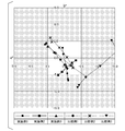
- FIG. 3 shows that light is incident on the surfaces of the optical laminates of Examples 1 to 3 and Comparative Examples 1 to 3 at incident angles of 5 °, 10 °, 20 °, 30 °, 40 °, and 50 °.
- FIG. 4 is an enlarged graph showing the central portion of the graph of FIG.
- FIG. 5 is a photograph of a test piece when light is incident on the surface of each optical laminate at incident angles of 5 °, 10 °, 20 °, 30 °, and 40 °.
- the present inventors have conducted intensive studies as shown below.
- the present inventors have been able to visually recognize an article in order to obtain an optical laminate in which the reflected light reflected by the article provided with the optical laminate is difficult to be colored and color unevenness is hardly visually recognized even if the viewing angle of the article is changed. Focusing on the relationship between the angle and the chromaticity (saturation and hue) of the reflected light, we made extensive studies.
- the present inventors have found that not only the saturation of the reflected light but also the change in the hue of the reflected light by changing the viewing angle has a great influence on the visibility of the color unevenness. Then, the present inventors sufficiently reduce the saturation of the reflected light when light having an incident angle of 30 ° to 40 ° is incident on the surface, and the incident angle is within the range of 5 ° to 30 °. It was found that by reducing the change in hue of the reflected light when light is incident, color unevenness is less likely to be visually recognized even if the viewing angle of the article is changed.
- the present inventors have incidented the saturation of the reflected light when light having an incident angle of 30 ° to 40 ° is incident on the surface, and the light within the range of the incident angle of 5 ° to 30 °.
- the saturation of the reflected light when the light is incident at an incident angle of 5 ° is higher than that when the light is incident at an incident angle of 30 ° to 40 °. It was found that even if it is large, it is difficult to visually recognize the coloring of the reflected light reflected on the article.
- the present inventors consider the reflected light when the light is incident on the surface at an incident angle of 30 ° to 40 ° and when the light is incident at an incident angle of 5 °.
- the chromaticity range and the change in the hue of the reflected light when light in the range of the incident angle of 5 ° to 30 ° was incident on the surface were repeatedly studied.
- the a * value and b * value of the reflected light in the CIE-Lab color system when light having a wavelength of 380 nm to 780 nm by the standard light source D65 is incident satisfies the following (condition A) to (condition C). It has been found that an optical laminate may be used.
- FIG. 1 is a schematic cross-sectional view showing an example of the optical laminate of the present invention.
- a transparent base material 2 a hard coat layer 3, an antireflection layer 4 (laminate), and an antifouling layer 5 are laminated in this order.
- the optical laminate 1 shown in FIG. 1 is provided in an article (not shown). Examples of the article include those provided with the optical laminate 1 on the surface of an image display device (not shown).
- FIG. 2 describes the a * value and the b * value of the reflected light in the CIE-Lab color system when light having a wavelength of 380 nm to 780 nm is incident on the optical laminate shown in FIG. 1 by the standard light source D65.
- the a * value and the b * value indicate the chromaticity, and the larger the absolute value of the a * value and the b * value is, the larger the saturation is. That is, in FIG. 2, the larger the absolute value of the a * value and the b * value is, the more vivid the color is, and the smaller the absolute value of the a * value and the b * value is, the more vivid the color is. , A color close to achromatic.
- the coordinates of + a * are the hues in the red direction
- the coordinates of -a * are the hues in the green direction
- the coordinates of + b * are the hues in the yellow direction
- the coordinates of -b * are the hues in the blue direction.
- the third quadrant (-a * , -b * ) corresponds to red to orange to yellow, yellow to yellowish green to green, green to bluish green to blue, and blue to purple to red.
- the hue of the reflected light changes to another quadrant depending on the incident angle (when a quadrant straddle occurs), the hue changes significantly, so that color unevenness becomes easily visible. It is preferable that the hue quadrant of the reflected light does not change depending on the incident angle, in other words, the hue of the reflected light stays within the same quadrant depending on the incident angle.
- the a * value and b * value of the reflected light in the CIE-Lab color system when light having a wavelength of 380 nm to 780 nm is incident from the standard light source D65 are as described above (condition A). )-(Condition C) is satisfied.
- Each of the above conditions (Condition A) to (Condition C) applies to the transparent base material 2 forming the optical laminate 1, the hard coat layer 3, the antireflection layer 4, and the antifouling layer 5. It can be adjusted by appropriately selecting the material and thickness.
- the a * value and b * value of the reflected light when light is incident on the surface of the optical laminate 1 at an incident angle of 30 ° to 40 ° are absolute values, respectively. 3 or less (in the region indicated by reference numeral A in FIG. 2) (condition A). Therefore, in the optical laminate 1 of the present embodiment, the saturation of the reflected light when light is incident at an incident angle of 30 ° to 40 ° is sufficiently small, and color unevenness due to changing the viewing angle of the article is visually recognized. It is hard to be done.
- the a * value and the b * value described above are preferably 2.5 or less in absolute value, respectively.
- the color unevenness caused by changing the viewing angle of the article becomes the optical laminate 1 that is more difficult to be visually recognized. If either one or both of the above a * and b * values exceeds 3 in absolute value, the saturation of the reflected light when light is incident at an incident angle of 30 ° to 40 ° is high. Therefore, color unevenness due to changing the viewing angle of the article becomes easy to be visually recognized.
- the optical laminate 1 shown in FIG. 1 has a * value and b * value of reflected light when light is incident on the surface of the optical laminate 1 at incident angles of 5 °, 10 °, 20 °, and 30 °.
- condition B ⁇ Maximum value of (
- is a numerical value corresponding to the hue of the reflected light.
- is less than 1.0 emits light at an incident angle of 5 ° to 30 °.
- the hue change of the reflected light is small when it is made to move. That is, the reflected light when the light is incident at an incident angle of 5 ° to 30 ° has similar hues. Therefore, in the optical laminate 1 of the present embodiment, the hue change of the reflected light due to the change in the viewing angle of the article is small, and the color unevenness is hard to be visually recognized.
- the hue change of the reflected light due to the change in the viewing angle of the article is large, so that the color unevenness is easily recognized.
- is preferably 0.5 or less, and more preferably 0.3 or less.
- the optical laminate 1 of the present embodiment satisfies the above (condition A) and (condition B), the saturation of the reflected light when light is incident at an incident angle of 30 ° to 40 ° is sufficiently small (FIG. In No. 2, the hue change of the reflected light when light is incident at an incident angle of 5 ° to 30 ° (within the region indicated by reference numeral A) is sufficiently small (satisfies the equation (B1)).
- the chromaticity (saturation and hue) of the reflected light of the optical laminate 1 changes continuously by changing the viewing angle of the article. Therefore, the optical laminate 1 satisfying the above (condition A) and (condition B) has, for example, the reflected light having a similar hue when light having an incident angle of 5 ° to 30 ° is continuously incident.
- the optical laminate 1 of the present embodiment has a sufficiently small saturation of reflected light when light is incident at an incident angle of 30 ° to 40 ° (condition A), and therefore, when the incident angle is 30 ° to 40 °. Even if the hue of the reflected light is different when the incident angle is 5 ° to 30 °, it is difficult to visually recognize the color unevenness. Therefore, in the optical laminate 1 of the present embodiment, color unevenness due to changing the viewing angle of the article is less likely to be visually recognized.
- one or both of the a * value and the b * value of the reflected light when light is incident on the surface of the optical laminate 1 at an incident angle of 5 ° is an absolute value of 5.
- the a * value and the b * value are in the range of 15 or less in absolute value (condition C).
- reference numeral C indicates a region in which the a * value and the b * value are 5 or more and 15 or less in absolute value.
- the above a * value and b * value are preferably 10 or less in absolute value, respectively. In this case, the colored light reflected on the article becomes the optical laminate 1 which is more difficult to see.
- the saturation of the reflected light when light is incident at an incident angle of 5 ° is an incident angle of 30. Even when light is incident at ° to 40 ° (inside the region indicated by reference numeral A in FIG. 2) and outside (for example, in the region indicated by reference numeral C in FIG. 2), it is reflected by the article. It is difficult to see the coloring of the reflected light. However, if either one or both of the above a * and b * values exceeds 15 in absolute value, the saturation of the reflected light when light is incident at an incident angle of 5 ° is large, and therefore the saturation of the reflected light is large. The coloring of the reflected light reflected on the article becomes easy to see.
- one or both of the a * value and the b * value of the reflected light when light is incident on the surface of the optical laminate 1 at an incident angle of 5 ° is absolute.
- the value is in the range of 5 or more (condition C). Therefore, for example, it is compared with the case where the a * value and the b * value of the reflected light when the light is incident at an incident angle of 5 ° are less than 3 (within the region indicated by the reference numeral A in FIG. 2).
- the material and thickness of each layer forming the optical laminate 1 and the choice of manufacturing method are increased, and the optical laminate 1 can be easily and efficiently manufactured.
- one or both of the above a * value and b * value may be 8 or more in absolute value.
- the material and thickness of each layer forming the optical laminate 1 and the selection of the manufacturing method are increased, and the manufacturing can be performed more easily and efficiently.
- the optical laminate 1 shown in FIG. 1 has a * values and b * values of reflected light in the CIE-Lab color system when the optical laminate 1 is incident on the surface of the optical laminate 1 at an incident angle of 5 ° to 25 °.
- the values are within the same quadrant on the a * b * plane (La * b * chromaticity diagram) (condition E). Therefore, for example, when the display device provided with the optical laminate of the present invention is provided on the center console of an automobile or on the front ceiling of the rear seat, the hue changes when visually recognized from the rear seat. There are few, and it is most suitable for these applications.
- the optical laminate 1 shown in FIG. 1 has an a * value of reflected light when light is incident on the surface of the optical laminate 1 at incident angles of 5 °, 10 °, 20 °, 30 °, and 40 °. It is preferable that the b * value satisfies the following formula (D1) (condition D). ⁇ Maximum value of (
- is less than 1.5 emits light at an incident angle of 5 ° to 40 °.
- the hue change of the reflected light is small when it is made to move. That is, the reflected light when the light is incident at an incident angle of 5 ° to 40 ° has similar hues. Therefore, in the optical laminate 1 of the present embodiment, the hue change of the reflected light due to the change in the viewing angle of the article is small, and the color unevenness is more difficult to be visually recognized.
- the a * value and b * value of the reflected light when light is incident on the surface of the optical laminate 1 at incident angles of 5 °, 10 °, 20 °, 30 °, and 40 ° are given by the following equation (D2). ) Is preferably satisfied, and more preferably the following formula (D3) is satisfied.
- the optical laminate 1 satisfies the formula (D2) or the formula (D3), the hue change of the reflected light due to the change in the viewing angle of the article becomes even smaller, and the color unevenness due to the change in the viewing angle of the article becomes even smaller. However, the optical laminate 1 is even more difficult to see.
- the transparent base material 2 As the transparent base material 2 forming the optical laminate 1 shown in FIG. 1, a known one can be used.
- the transparent base material 2 is made of a transparent material capable of transmitting light in the visible light region.
- the "transparent material” means a material having a light transmittance of 80% or more in the visible light region.
- a plastic film can be used as the transparent base material 2, for example.
- examples thereof include polyvinylidene chloride resin, polystyrene resin, polyvinyl alcohol resin, polyarylate resin, and polyphenylene sulfide resin.
- the material of the plastic film it is preferable to use any one or more selected from polyester resin, acetate resin, polycarbonate resin, and polyolefin resin, and in particular, triacetyl cellulose (TAC). ) Is preferably used.
- TAC triacetyl cellulose
- the transparent base material 2 may include a reinforcing material as long as the optical characteristics are not impaired.
- the reinforcing material include cellulose nanofibers and nanosilica.
- an inorganic material such as a glass film may be used as the transparent base material 2.
- a film to which an optical function and / or a physical function is imparted may be used, if necessary.
- the film having an optical function and / or a physical function include a polarizing plate film, a retardation compensation film, a heat ray blocking film, a conductive film, and a brightness improving film.
- a film having an optical function and / or a physical function may be used, for example, having a function such as an antistatic function.
- the thickness of the transparent substrate 2 is, for example, preferably 25 ⁇ m or more, and more preferably 40 ⁇ m or more.
- the thickness of the transparent base material 2 is 25 ⁇ m or more, wrinkles are less likely to occur even if stress is applied to the optical laminate 1, which is preferable.
- the thickness of the transparent base material 2 is 25 ⁇ m or more, wrinkles are less likely to occur in the transparent base material 2 even if the hard coat layer 3 is formed on the transparent base material 2 when the optical laminate 1 is manufactured. Can be manufactured with good yield.
- the thickness of the transparent base material 2 is 25 ⁇ m or more, when the optical laminate 1 is manufactured, the optical laminate 1 in the middle of production is less likely to curl and is easy to handle, which is preferable.
- the thickness of the transparent substrate 2 is, for example, preferably 300 ⁇ m or less, and more preferably 250 ⁇ m or less.
- the thickness of the transparent base material 2 is 300 ⁇ m or less, it is possible to prevent the transparent base material 2 from being hindered in thinning and weight reduction due to the thick thickness of the transparent base material 2.
- the optical laminate 1 can be efficiently manufactured by using the transparent base material 2 wound in a roll shape.
- the thickness of the transparent base material 2 is 300 ⁇ m or less, water and organic substances are less likely to be generated from the transparent base material 2 when the hard coat layer 3 is formed on the transparent base material 2, and the production can be performed with good yield.
- the method for producing the transparent base material 2 is not particularly limited, and the transparent substrate 2 can be produced by a known production method.
- a surface-treated transparent substrate 2 may be used.
- the surface treatment method include sputtering, corona discharge, ultraviolet irradiation, electron beam irradiation, etching treatment such as chemical conversion and oxidation, and undercoating treatment.
- a transparent base material 2 having good adhesion to the hard coat layer 3 can be obtained. Be done.
- the surface of the transparent base material 2 may be washed, if necessary, before the hard coat layer 3 is formed on the transparent base material 2.
- the method for cleaning the surface of the transparent substrate 2 include solvent cleaning and ultrasonic cleaning. Cleaning the transparent base material 2 is preferable because the surface of the transparent base material 2 can be dust-removed and the surface is cleaned.
- Hard coat layer As the hard coat layer 3, known ones can be used, and examples thereof include those containing a binder resin and a filler.
- the hard coat layer 3 may contain a known material such as a leveling agent, if necessary, in addition to the binder resin and the filler.
- the binder resin contained in the hard coat layer 3 it is preferable to use a transparent material.
- the binder resin for example, an ionizing radiation curable resin, a thermoplastic resin, a thermosetting resin, or the like can be used. Only one kind of binder resin may be used, or two or more kinds of binder resins may be mixed and used.
- the ionizing radiation curable resin examples include ethyl (meth) acrylate, ethylhexyl (meth) acrylate, styrene, methylstyrene, N-vinylpyrrolidone, urethane acrylate, polyethylene glycol diacrylate, pentaerythritol triacrylate (PETA), and dipenta.
- ethyl (meth) acrylate ethylhexyl (meth) acrylate
- styrene methylstyrene
- N-vinylpyrrolidone urethane acrylate
- polyethylene glycol diacrylate pentaerythritol triacrylate
- PETA pentaerythritol triacrylate
- dipenta examples thereof include erythritol hexaacrylate (DPHA) and pentaerythritol tetraacrylate (PETTA).
- ionizing radiation curable resin a resin obtained by modifying the above-mentioned compound with PO (propylene oxide), EO (ethylene oxide), CL (caprolactone) or the like may be used.
- PO propylene oxide
- EO ethylene oxide
- CL caprolactone
- (meth) acrylate means methacrylate and / or acrylate.
- the hard coat layer 3 may contain a known ionizing radiation curing initiator.
- the ionizing radiation curable resin contains an ultraviolet curable resin such as (meth) acrylate, it preferably contains an ultraviolet curable initiator such as hydroxy-cyclohexyl-phenyl-ketone.
- thermoplastic resin examples include styrene resin, (meth) acrylic resin, vinyl acetate resin, vinyl ether resin, halogen-containing resin, alicyclic olefin resin, polycarbonate resin, polyester resin, and polyamide resin. , Cellulose derivatives, silicone resins and the like.
- thermosetting resin examples include phenol resin, urea resin, diallyl phthalate resin, melamine resin, guanamine resin, unsaturated polyester resin, polyurethane resin, epoxy resin, aminoalkyd resin, melamine-urea cocondensation resin, and silicon resin.
- thermosetting resin examples include polysiloxane resins (including so-called silsesquioxane such as cage-like and ladder-like).
- Various fillers contained in the hard coat layer 3 can be selected depending on the use of the optical laminate 1 from the viewpoints of antiglare property, adhesion to the antireflection layer 4 described later, and antiblocking property.
- known particles such as silica (Si oxide) particles, alumina (aluminum oxide) particles, and organic fine particles can be used.
- organic fine particles made of an acrylic resin or the like as the filler.
- the particle size of the organic fine particles is preferably 10 ⁇ m or less, more preferably 5 ⁇ m or less, and particularly preferably 3 ⁇ m or less.
- silica particles is preferably 800 nm or less, and particularly preferably 100 nm or less.
- the thickness of the hard coat layer 3 is, for example, preferably 0.5 ⁇ m or more, and more preferably 1 ⁇ m or more.
- the thickness of the hard coat layer 3 is preferably 100 ⁇ m or less.
- the hard coat layer 3 may be composed of a single layer, or may be a stack of a plurality of layers.
- the method for producing the hard coat layer 3 is not particularly limited, and the hard coat layer 3 can be produced by a known production method.
- the hard coat layer 3 can be manufactured by a coating method.
- the coating method include a method in which a coating liquid obtained by dissolving and / or dispersing the material to be the hard coat layer 3 in a solvent is applied onto the transparent substrate 2 by a known method and cured. ..
- a known solvent can be used and can be appropriately determined depending on the material to be the hard coat layer 3.
- the antireflection layer 4 is formed from a laminate in which low refractive index material layers 4a and 4c and high refractive index material layers 4b made of a material having a higher refractive index than low refractive index material layers 4a and 4c are alternately laminated. Become.
- the antireflection layer 4 diffuses the light incident on the optical laminate 1 from the antifouling layer 5 side.
- the optical laminate 1 functions as an antireflection film that prevents light incident on the optical laminate 1 from the antifouling layer 5 side from being emitted in one direction as reflected light.
- the low refractive index material layer 4a arranged in contact with the hard coat layer 3 has the antireflection layer 4 and the hard coat layer 3. It has a function as an adhesion layer for adhesion. Further, in the optical laminate 1 shown in FIG. 1, a low refractive index material layer 4c is arranged in contact with the antifouling layer 5 on the surface of the antireflection layer 4 opposite to the hard coat layer 3.
- the antireflection layer 4 has a low refractive index material layer 4a, a high refractive index material layer 4b, a low refractive index material layer 4c, and a high refractive index in order from the hard coat layer 3 side.
- a laminated body in which five layers of the material layer 4b and the low refractive index material layer 4c are laminated is taken as an example.
- the number of layers of the low refractive index material layers 4a and 4c forming the antireflection layer 4 and the high refractive index material layer 4b is not limited to five, and may be less than five or five. It may be super-layered, and can be appropriately determined according to the optical characteristics required for the antireflection layer 4.
- the plurality of low refractive index material layers 4a and 4c all have the same refractive index. Alternatively, some or all of them may have different refractive indexes.
- the laminate forming the antireflection layer 4 includes two or more high refractive index material layers 4b, the plurality of high refractive index material layers 4b may all have the same refractive index. Some or all of the refractive indexes may be different.
- the refractive index of the low refractive index material layers 4a and 4c is preferably 1.20 to 1.60, and more preferably 1.30 to 1.50.
- the low refractive index material layers 4a and 4c preferably contain SiO 2 (Si oxide) as a main component.
- the low refractive index material layers 4a and 4c may be composed of only Si oxide, or may be different from Si oxide in a range of 50% by mass or less, preferably 10% by mass or less. It may contain elements.
- Na may be contained in order to improve the durability of the low refractive index material layers 4a and 4c, and Zr, Al, in order to improve the hardness of the low refractive index material layers 4a and 4c. It may contain one or more elements selected from N.
- the refractive index of the high refractive index material layer 4b is preferably 2.00 to 2.60, and more preferably 2.10 to 2.45.
- the high refractive index material layer 4b include niobium pentoxide (Nb 2 O 5 , refractive index 2.33), titanium oxide (TiO 2 , refractive index 2.33 to 2.55), and tungsten oxide (WO 3 , Refractive index 2.2), cerium oxide (CeO 2 , refractive index 2.2), tantalum pentoxide (Ta 2 O 5 , refractive index 2.16), zinc oxide (ZnO, refractive index 2.1), indium oxide Examples thereof include those made of tin (ITO, refractive index 2.06), and those made of niobium pentoxide are preferable.
- the film thicknesses of the low refractive index material layers 4a and 4c and the high refractive index material layer 4b constituting the antireflection layer 4 can be appropriately determined according to the optical characteristics required for the antireflection layer 4.
- the film thicknesses of the low refractive index material layers 4a and 4c and the high refractive index material layer 4b may all be the same, or some or all of them may be different from each other.
- the film thickness of the low refractive index material layers 4a and 4c can be, for example, 1 nm or more and 200 nm or less.
- the plurality of low refractive index material layers 4a and 4c may all have the same film thickness, or a part or a part thereof. All film thicknesses may be different.
- the film thickness of the high refractive index material layer 4b can be, for example, 1 nm or more and 200 nm or less.
- the plurality of high refractive index material layers 4b may all have the same film thickness, or a part or all of the film thickness. May be different.
- the thickness of the low refractive index material layers 4a and 4c and the high refractive index material layer 4b is, for example, 30 to 120 nm in order from the hard coat layer 3 side, and the high refractive index material layers 4a and 10 to 50 nm. It can be 4b, a low refractive index material layer 4c of 30 to 120 nm, a high refractive index material layer 4b of 50 to 200 nm, and a low refractive index material layer 4c of 50 to 200 nm.
- the method for producing the antireflection layer 4 is not particularly limited, and the antireflection layer 4 can be produced by a known production method.
- the antireflection layer 4 is formed on, for example, a hard coat layer 3 by a sputtering method to obtain a low refractive index material layer 4a, a high refractive index material layer 4b, a low refractive index material layer 4c, a high refractive index material layer 4b, and a low refractive index. It can be produced by the method of forming the material layer 4c in this order.
- the low refractive index material layers 4a and 4c and the high refractive index material layer 4b are formed by a sputtering method, they are denser than those formed by a general vacuum vapor deposition method or a coating method. It will be something like that. As a result, the optical laminate 1 having good durability and having a water vapor permeability of 1.0 g / m 2 / day or less is obtained.
- the antifouling layer 5 is provided on the surface of the antireflection layer 4 opposite to the hard coat layer 3, if necessary.
- the antifouling layer 5 prevents the optical laminate 1 from being soiled and suppresses the antireflection layer 4 from being worn.
- the antifouling layer 5 preferably contains a fluorine-based compound.
- a fluorine-based compound for example, a compound composed of a fluorine-modified organic group and a reactive silyl group such as alkoxysilane is preferably used. Examples of such a compound include perfluorodecyltriethoxysilane (FDTS).
- FDTS perfluorodecyltriethoxysilane
- Examples of commercially available products suitable as materials for the antifouling layer 5 include Optool DSX (manufactured by Daikin Industries, Ltd.) and KY-1203 (manufactured by Shin-Etsu Chemical Co., Ltd.).
- the antifouling layer 5 contains a light stabilizer, an ultraviolet absorber, a colorant, an antistatic agent, a lubricant, a leveling agent, an antifoaming agent, an antioxidant, a flame retardant, an infrared absorber, and a surfactant, if necessary. Additives such as may be included.
- the thickness of the antifouling layer 5 can be, for example, 1 to 20 nm, preferably 3 to 10 nm.
- the method for producing the antifouling layer 5 is not particularly limited, and the antifouling layer 5 can be produced by a known production method, and is appropriately selected in consideration of the required durability and cost.
- the antifouling layer 5 can be produced by a coating method or a vapor deposition method. Examples of the coating method include a method in which a coating liquid in which a material to be an antifouling layer 5 is dissolved in a solvent is applied onto the antireflection layer 4 by a known method and dried.
- the antifouling layer 5 is formed by the vapor deposition method, for example, it is denser and has excellent adhesion to the antireflection layer 4 as compared with the antifouling layer formed by the coating method. Therefore, the antifouling layer 5 formed by the vapor deposition method has high wear resistance.
- one or more layers may be provided on the surface of the transparent base material 2 opposite to the antireflection layer 3, if necessary.
- An adhesive layer for adhering the optical laminate 1 to another member such as the surface of an image display device may be provided on the surface of the transparent base material 2 opposite to the antireflection layer 3.
- the pressure-sensitive adhesive layer and other optical films may be laminated in this order. Examples of other optical films include a polarizing film, a retardation compensation film, a 1/2 wave plate, and a 1/4 wave plate. Further, the other optical film described above may be formed in contact with the surface of the transparent base material 2 opposite to the antireflection layer 3.
- the transparent base material 2, the hard coat layer 3, and the antireflection layer 4 are laminated in this order, and the antireflection layer 4 includes the low refractive index material layers 4a and 4c. It is composed of a laminated body in which high refractive index material layers 4b made of a material having a higher refractive index than low refractive index material layers 4a and 4c are alternately laminated.
- the a * value and the b * value of the reflected light in the CIE-Lab color system when light having a wavelength of 380 nm to 780 nm is incident by the standard light source D65 are the above (conditions). A)-(Condition C) are satisfied.
- the optical laminate 1 of the present embodiment due to the synergistic effect of satisfying the above (condition A) to (condition C), it is difficult to color the reflected light reflected by the article and the article is visually recognized. Even if the angle is changed, color unevenness becomes difficult to see.
- the article of the present embodiment includes the optical laminate 1 of the present embodiment.
- the optical laminate 1 may be provided on the surface of the image display device.
- the image display device include a flat panel display (FPD) such as a liquid crystal display panel and an organic electroluminescence (EL) display panel.
- FPD flat panel display
- EL organic electroluminescence
- Examples of the surface of the image display device to which the optical laminate 1 of the present embodiment is attached include a mobile phone screen, a smartphone screen, a tablet terminal screen, a personal computer display, a navigation system screen, and an operation of a game machine.
- Examples include screens of information input terminals such as screens, operation screens of operation support devices such as aircraft and trains, and lightning display boards.
- the image display device to which the optical laminate 1 is attached is preferably an image display device that can be visually recognized at various viewing angles when used, and in particular, a navigation system screen, a mobile phone screen, or a smartphone. It is preferably a screen.
- the article of the present embodiment is not limited to the one in which the optical laminate 1 is provided on the surface of the image display device.
- a window glass, goggles, a light receiving surface of a solar cell, a glass table surface, an instrument panel, an optical sensor surface, a helmet visor, a mirror, a head-mounted display, etc. on which the optical laminate 1 of the present embodiment is provided on the surface.
- the surface provided with the optical laminate 1 may be flat or curved.
- the article of the present embodiment includes the optical laminate 1 of the present embodiment, the reflected light from the article is less likely to be colored, and uneven color is less likely to be visually recognized even if the viewing angle is changed.
- the article of the present embodiment has the optical laminate 1 provided on the surface of the image display device, the reflected light from the image display device is less likely to be colored, and color unevenness is visually recognized even if the viewing angle is changed. It is difficult to do and is preferable.
- the optical laminate 1 shown in FIG. 1 was produced by the method shown below. First, as the transparent base material 2, a film made of triacetyl cellulose (TAC) having a thickness of 80 ⁇ m was prepared. Then, a hard coat layer 3 having a thickness of 5 ⁇ m made of the materials shown in Table 1 was formed on the transparent base material 2.
- TAC triacetyl cellulose
- CHC shown in Table 1 was formed by a method in which a coating liquid having the composition shown in Table 2 was applied onto a transparent substrate 2 using a bar coater, irradiated with ultraviolet rays, photopolymerized, and cured.
- AG-HC shown in Table 1 is obtained by applying a coating liquid having the composition shown in Table 3 on a transparent substrate 2 using a bar coater, and irradiating with ultraviolet rays to photopolymerize and cure the coating liquid. Formed.
- the antireflection layer 4 (laminated body) is formed on the hard coat layer 3 by a reactive sputtering method using a Si target and an Nb target as sputtering targets and a mixed gas of Ar gas and O 2 gas.
- the hard coat layer 3 has the film thickness shown in Table 1, the low refractive index material layer 4a (first layer) made of Si oxide that may be oxygen deficient, and the film thickness shown in Table 1.
- the high refractive index material layer 4b (fourth layer) made of Nb 2 O 5 having Nb 2 O 5 and the low refractive index material layer 4c (fifth layer) made of SiO 2 having the film thickness shown in Table 1 are repeated in this order. A film was formed.
- the coating liquid was applied onto the antireflection layer 4 using a coil bar (product name: No. 579, rod No. 9, manufactured by Yasuda Seiki Seisakusho Co., Ltd.) so that the film thickness of the coating film was 10 ⁇ m.
- the antifouling layer 5 having a film thickness of 10 nm was formed by a method of drying at 80 ° C. for 2 minutes.
- As the coating solution 0 is an alkoxysilane compound (trade name: Optool DSX, manufactured by Daikin Industries, Ltd.) having a perfluoropolyether group in a fluorine solvent (trade name: Florinate FC-3283: manufactured by 3M Japan Co., Ltd.). A solution containing 1% by mass was used.
- Comparative Example 2 The optical laminate of Comparative Example 2 was produced by performing the steps up to the formation of the antireflection layer 4 in the same manner as in Examples 1 to 3, Comparative Example 1, and Comparative Example 3.
- Comparative Example 4 In the production of the optical laminate of Comparative Example 4, a film made of triacetyl cellulose (TAC) having a thickness of 80 ⁇ m was prepared as the transparent base material 2, and a high refractive index layer and a low refractive index layer were coated on the base material. Formed by law.
- TAC triacetyl cellulose
- the solid content is a substance other than the solvent in the coating liquid, and here, it is a photopolymerizable prepolymer such as dipentaerythritol hexaacrylate, antimony pentoxide, and an initiator.
- This coating liquid for a high refractive index layer is applied to the surface of a triacetyl cellulose film (thickness 80 ⁇ m) which is a transparent base material by a gravure method so as to have a drying thickness of 4 ⁇ m, and dried in an oven at 80 ° C. for 1 minute and 30 seconds. After that, it was cured by irradiating a 160 W high-pressure mercury lamp from a distance of 18 cm for 3 seconds to form a high refractive index layer.
- This high refractive index layer also functions as a hard coat layer.
- a low refractive index coating agent (polymerizable composition) was prepared by adding 8% by weight of the agent and 1.5% by weight of a modified silicone compound (functional group equivalent: 3900 g / mol).
- a low refractive index coating agent was dissolved and dispersed in n-butanol as a solvent to prepare a coating liquid for a low refractive index layer having a solid content (low refractive index coating agent) of 3.0% by weight.
- a coating solution for a low refractive index layer is applied to the surface of the high refractive index layer using a gravure method so as to have a dry film thickness of 100 nm to form a coating layer, and after drying in an oven at 80 ° C. for 1 minute and 30 seconds, In a nitrogen atmosphere (oxygen concentration 1000 ppm), the coating layer was cured by irradiating light from a high-pressure mercury lamp at a distance of 18 cm from a 160 W high-pressure mercury lamp for 3 seconds to form a low refractive index layer. An antireflection film of No. 4 was obtained.
- Comparative Example 5 The optical laminate of Comparative Example 5 was obtained by the production method described in JP-A-2019-70756.
- the incident light was incident at 5 °, and the chromaticity of the reflected light was calculated from the reflected spectrum using a calculation formula. As the chromaticity, the a * value and the b * value in the CIE-Lab color system were calculated. The results are shown in Table 1. Further, Examples 1 to 3 and Comparative Examples 1 to 3 are also shown in FIGS. 3 and 4.
- the incident angles of 10 °, 20 °, 25 °, and 30 ° are the same as when the light is incident on the surface of the optical laminate at an incident angle of 5 °.
- the chromaticity of the reflected light was calculated by incident light at 40 ° and 50 °.
- Table 1 Further, Examples 1 to 3 and Comparative Examples 1 to 3 are shown in FIGS. 3 and 4.
- FIG. 3 shows that light is incident on the surfaces of the optical laminates of Examples 1 to 3 and Comparative Examples 1 to 3 at incident angles of 5 °, 10 °, 20 °, 30 °, 40 °, and 50 °. It is a graph which showed the chromaticity of the reflected light when it was made.
- FIG. 4 is an enlarged graph showing the central portion of the graph of FIG. In FIG. 4, the number written in the vicinity of the point on the coordinates is the incident angle (°) corresponding to the point on the coordinates.
- Martens hardness measurement Using a Fisher picodenter HM-500 and a Vickers indenter, the Martens hardness under a pushing load of 0.1 mN was measured. Then, it was evaluated according to the following criteria. "standard” ⁇ : 1000 (N / mm 2 ) or more. X: Less than 1000 (N / mm 2).
- Step wool sliding performance test Using a friction tester type I conforming to JIS L0849, the friction body was reciprocated horizontally along the surface of the optical laminate (test piece) of Example 1 and Comparative Example 2 to obtain a test piece. Steel wool (# 0000 manufactured by Bonstar Co., Ltd.) was used as the friction body. The test settings were a load of 1000 g / cm 2 , a stroke of 75 mm, a speed of 150 mm / s, and it was tested whether or not scratches were formed when sliding with 10 reciprocating steel wool (SW). Then, it was evaluated according to the following criteria. ⁇ : When there is no scratch. ⁇ : When scratches occur.
- the optical laminates of Examples 1 to 3 satisfying the above-mentioned (Condition A) to (Condition D) are illuminated at an incident angle of 5 ° to 40 °.
- the change in hue of the reflected light was small when the light was incident.
- the optical laminates of Examples 1 to 3 have similar hues in the reflected light when light having an incident angle of 5 ° to 40 ° is continuously incident. It was confirmed that the saturation tends to decrease as the incident angle increases. Further, as shown in Table 1, the results of visual evaluation of the optical laminates of Examples 1 to 3 were " ⁇ ".
- Examples 1 to 3 satisfy (Condition E) in addition to satisfying (Condition A) to (Condition D). That is, in Examples 1 to 3, the a * value and b * value in the CIE-Lab color system of the reflected light when incident at an incident angle of 5 ° to 25 ° do not change to different quadrants and are within the same quadrant. Stay in. This means, for example, when the display device provided with the optical laminates of Examples 1 to 3 is provided on the center console of an automobile or on the front ceiling of the rear seats, the color tone when visually recognized from the rear seats. It shows that there is little change and it is suitable for such applications.
- the optical laminates of Comparative Examples 1 to 3 that do not satisfy any one or more of the above-mentioned conditions (Condition A) to (Condition C) are as shown in Tables 1, 3 and 4.
- the hue change of the reflected light when light was incident at an incident angle of 5 ° to 40 ° was large.
- the optical laminates of Comparative Examples 1 to 3 had a visual evaluation result of "x".
- the purple hue is visually recognized at the incident angles of 5 ° and 10 °
- the yellow-green hue is visually recognized at the incident angles of 20 ° and 30 °
- a green hue is visually recognized. That is, in the optical laminate of Comparative Example 2, the hues of the colors visually recognized are different between the incident angles of 5 ° and 10 °, the incident angles of 20 ° and 30 °, and the incident angles of 40 °.
- a blue hue is visually recognized at an incident angle of 5 ° and 10 °
- a purple hue is visually recognized at an incident angle of 20 °
- a reddish purple color is visually recognized at an incident angle of 30 ° and 40 °. Hue is visible. That is, in the optical laminate of Comparative Example 3, the hues of the colors visually recognized are different between the incident angles of 5 ° and 10 °, the incident angles of 20 °, and the incident angles of 30 ° and 40 °, respectively.
- an antireflection layer was prepared by coating to obtain an optical laminate.
- an antireflection layer was prepared by sputtering, and an antifouling layer was formed on the antireflection layer to obtain optics. It was found that the hardness was remarkably lowered as compared with Examples 1 to 3 and Comparative Examples 1 to 3 in which the laminated body was obtained. This is because the inorganic thin film is formed by sputtering, so that a film that is denser and harder than the coating method is formed.
- the steel wool sliding performance test it was found that in Comparative Example 4 and Comparative Example 5, the steel wool sliding resistance was lower than that in Examples 1 to 3 and Comparative Examples 1 to 3.
Landscapes
- Physics & Mathematics (AREA)
- General Physics & Mathematics (AREA)
- Optics & Photonics (AREA)
- Chemical & Material Sciences (AREA)
- Nonlinear Science (AREA)
- Inorganic Chemistry (AREA)
- Mathematical Physics (AREA)
- Crystallography & Structural Chemistry (AREA)
- Chemical Kinetics & Catalysis (AREA)
- Engineering & Computer Science (AREA)
- Theoretical Computer Science (AREA)
- Laminated Bodies (AREA)
- Surface Treatment Of Optical Elements (AREA)
- Liquid Crystal (AREA)
- Devices For Indicating Variable Information By Combining Individual Elements (AREA)
Abstract
この光学積層体(1)では、透明基材(2)とハードコート層(3)と反射防止層(4)とがこの順に積層され、反射防止層(4)が低屈折率材料層(4a、4c)と高屈折率材料層(4b)とが交互に積層された積層体からなり、波長380nm~780nmの光を入射させたときの反射光のa*値およびb*値が、(条件A)~(条件C)、及び、(条件E)を満たし、反射防止層がスパッタ層であり、(条件A)入射角30°~40°で入射させた時の反射光のa*値およびb*値が絶対値で3以下であり、(条件B)入射角5°、10°、20°、30°で入射させた時の反射光のa*値およびb*値が所定の不等式を満たし、(条件C)入射角5°入射させた時の反射光のa*値およびb*値の一方または両方が絶対値で5以上かつ15以下の範囲であり、(条件E)入射角5°~25°で入射させたときのa*値およびb*値がa*b*平面上の同一象限内である。
Description
本発明は、光学積層体および物品に関する。
本願は、2020年3月23日に日本に出願された特願2020-051220号、及び、2021年3月17日に日本に出願された特願2021-043915号に基づき優先権を主張し、その内容をここに援用する。
本願は、2020年3月23日に日本に出願された特願2020-051220号、及び、2021年3月17日に日本に出願された特願2021-043915号に基づき優先権を主張し、その内容をここに援用する。
フラットパネルディスプレイ(FPD)などの画像表示装置は、携帯電話、スマートフォン、カーナビゲーション装置などに広く使用されている。
従来の画像表示装置においては、視認角度による色むらを視認し難くすることが要求されている。色むらは、視認角度によって色味(色度)が異なって見える現象である。
例えば、特許文献1には、標準光源D65による波長380nm~780nmの光Aを、入射角5°で入射させた際の視感度反射率が0.5%以下であり、該光Aの入射角を5°~50°の範囲で変化させた際の正反射光において、CIE-Lab表色系におけるa*値の最大値と最小値との差に対する、CIE-Lab表色系におけるb*値の最大値と最小値との差の比(b*値の差/a*値の差)が、2以上となる、反射防止フィルムが記載されている。
従来の画像表示装置においては、視認角度による色むらを視認し難くすることが要求されている。色むらは、視認角度によって色味(色度)が異なって見える現象である。
例えば、特許文献1には、標準光源D65による波長380nm~780nmの光Aを、入射角5°で入射させた際の視感度反射率が0.5%以下であり、該光Aの入射角を5°~50°の範囲で変化させた際の正反射光において、CIE-Lab表色系におけるa*値の最大値と最小値との差に対する、CIE-Lab表色系におけるb*値の最大値と最小値との差の比(b*値の差/a*値の差)が、2以上となる、反射防止フィルムが記載されている。
画像表示装置上に設置される反射防止膜などの光学積層体は、これが設置された画像表示装置に反射される反射光を着色しにくいことが好ましい。また、光学積層体としては、これが設置された画像表示装置の視認角度を変化させても、色むらが視認されないことが好ましい。
しかしながら、従来の光学積層体は、これが設置された画像表示装置の視認角度を異ならせることによって、色むらが視認される場合があった。
このため、画像表示装置に上に設置される従来の光学積層体においては、画像表示装置に反射される反射光を着色しにくく、かつ、画像表示装置の視認角度を変化させても色むらが視認されにくいものとすることが要求されている。
このため、画像表示装置に上に設置される従来の光学積層体においては、画像表示装置に反射される反射光を着色しにくく、かつ、画像表示装置の視認角度を変化させても色むらが視認されにくいものとすることが要求されている。
本発明は、上記事情を鑑みてなされたものであり、物品に備えられ、物品に反射される反射光を着色しにくく、物品の視認角度を変化させても色むらが視認されにくい光学積層体を提供することを目的とする。
また、本発明は、本発明の光学積層体が備えられ、反射光が着色されにくく、視認角度を変化させても色むらが視認されにくい物品を提供することを目的とする。
また、本発明は、本発明の光学積層体が備えられ、反射光が着色されにくく、視認角度を変化させても色むらが視認されにくい物品を提供することを目的とする。
上記課題を解決するために、この発明は以下の手段を提案している。
[1] 透明基材と、ハードコート層と、反射防止層とが、この順に積層され、
前記反射防止層が、低屈折率材料層と、前記低屈折率材料層よりも高屈折率の材料からなる高屈折率材料層とが交互に積層された積層体からなり、
標準光源D65による波長380nm~780nmの光を入射させたときの反射光のCIE-Lab表色系におけるa*値およびb*値が、下記(条件A)~(条件C)を満たすことを特徴とする光学積層体。
前記反射防止層が、低屈折率材料層と、前記低屈折率材料層よりも高屈折率の材料からなる高屈折率材料層とが交互に積層された積層体からなり、
標準光源D65による波長380nm~780nmの光を入射させたときの反射光のCIE-Lab表色系におけるa*値およびb*値が、下記(条件A)~(条件C)を満たすことを特徴とする光学積層体。
(条件A)前記光を前記光学積層体の表面に対して入射角30°~40°で入射させた時の前記反射光の前記a*値および前記b*値が、それぞれ絶対値で3以下である。
(条件B)前記光を前記光学積層体の表面に対して入射角5°、10°、20°、30°で入射させた時の前記反射光の前記a*値および前記b*値が、以下の式(B1)を満たす。
{(|a*|/|b*|)の最大値}-{(|a*|/|b*|)の最小値}<1.0‥‥(B1)
(条件C)前記光を前記光学積層体の表面に対して入射角5°で入射させた時の前記反射光の前記a*値と前記b*値の一方または両方が絶対値で5以上であり、前記a*値および前記b*値が絶対値で15以下の範囲である。
(条件E)入射角5°~25°で入射させたときの反射光のCIE-Lab表色系におけるa*値およびb*値が、a*b*平面上の同一象限内である。
[2] 前記光を入射させたときの反射光のCIE-Lab表色系におけるa*値およびb*値が、下記(条件D)を満たすことを特徴とする[1]に記載の光学積層体。
(条件D)前記光を前記光学積層体の表面に対して入射角5°、10°、20°、30°、40°で入射させた時の前記反射光の前記a*値および前記b*値が、以下の式(D1)を満たす。
{(|a*|/|b*|)の最大値}-{(|a*|/|b*|)の最小値}<1.5‥‥(D1)
(条件D)前記光を前記光学積層体の表面に対して入射角5°、10°、20°、30°、40°で入射させた時の前記反射光の前記a*値および前記b*値が、以下の式(D1)を満たす。
{(|a*|/|b*|)の最大値}-{(|a*|/|b*|)の最小値}<1.5‥‥(D1)
[3] 前記(条件D)において、前記光を前記光学積層体の表面に対して入射角5°、10°、20°、30°、40°で入射させた時の前記反射光の前記a*値および前記b*値が、以下の式(D2)を満たす[2]に記載の光学積層体。
{(|a*|/|b*|)の最大値}-{(|a*|/|b*|)の最小値}<1.0‥‥(D2)
[4] 前記(条件D)において、前記光を前記光学積層体の表面に対して入射角5°、10°、20°、30°、40°で入射させた時の前記反射光の前記a*値および前記b*値が、以下の式(D3)を満たす[2]に記載の光学積層体。
{(|a*|/|b*|)の最大値}-{(|a*|/|b*|)の最小値}<0.1‥‥(D3)
{(|a*|/|b*|)の最大値}-{(|a*|/|b*|)の最小値}<1.0‥‥(D2)
[4] 前記(条件D)において、前記光を前記光学積層体の表面に対して入射角5°、10°、20°、30°、40°で入射させた時の前記反射光の前記a*値および前記b*値が、以下の式(D3)を満たす[2]に記載の光学積層体。
{(|a*|/|b*|)の最大値}-{(|a*|/|b*|)の最小値}<0.1‥‥(D3)
[5] 前記低屈折率材料層がSi酸化物を含有し、前記高屈折率材料層がNb2O5からなる[1]~[4]のいずれかに記載の光学積層体。
[6] 前記低屈折率材料層および前記高屈折率材料層が、スパッタ法により形成されたものである[5]に記載の光学積層体。
[6] 前記低屈折率材料層および前記高屈折率材料層が、スパッタ法により形成されたものである[5]に記載の光学積層体。
[7] 前記反射防止層の前記バーコード層と反対側の面に、防汚層が積層されている[1]~[6]のいずれかに記載の光学積層体。
[8] 前記防汚層がフッ素系化合物を含有し、蒸着法または塗布法により形成されたものである[7]に記載の光学積層体。
[8] 前記防汚層がフッ素系化合物を含有し、蒸着法または塗布法により形成されたものである[7]に記載の光学積層体。
[9] [1]~[8]のいずれかに記載の光学積層体を備えることを特徴とする物品。
[10] 前記光学積層体が、画像表示装置の表面に備えられている[9]に記載の物品。
[10] 前記光学積層体が、画像表示装置の表面に備えられている[9]に記載の物品。
本発明の光学積層体によれば、標準光源D65による波長380nm~780nmの光を入射させたときの反射光のCIE-Lab表色系におけるa*値およびb*値が、上記(条件A)~(条件C)を満たすことの相乗効果によって、物品に備えられ、物品に反射される反射光を着色しにくく、物品の視認角度を変化させても色むらが視認されにくいものとなる。
また、本発明の物品は、本発明の光学積層体を備えているので、物品からの反射光が着色されにくく、視認角度を変化させても色むらが視認されにくい。
また、本発明の物品は、本発明の光学積層体を備えているので、物品からの反射光が着色されにくく、視認角度を変化させても色むらが視認されにくい。
本発明者らは、上記課題を解決するために、以下に示すように鋭意研究を重ねた。
本発明者らは、光学積層体を備えた物品に反射される反射光を着色しにくく、物品の視認角度を変化させても色むらが視認されにくい光学積層体を得るために、物品の視認角度と反射光の色度(彩度および色相)との関係に着目して、鋭意検討を重ねた。
本発明者らは、光学積層体を備えた物品に反射される反射光を着色しにくく、物品の視認角度を変化させても色むらが視認されにくい光学積層体を得るために、物品の視認角度と反射光の色度(彩度および色相)との関係に着目して、鋭意検討を重ねた。
その結果、表面に対して入射角5°以下の小さい入射角で光を入射させたときの反射光の彩度が十分に小さくても、入射角30°~40°で光を入射させたときの反射光の彩度が大きいと、物品の視認角度を変化させることによる色むらが視認されやすいことが分かった。このことから、物品の視認角度を変化させることによる色むらを抑制するためには、表面に対して入射角30°~40°の光を入射させたときの反射光の彩度を小さくすることが重要であるという知見を得た。
また、本発明者らは、色むらの視認されやすさには、反射光の彩度だけでなく、視認角度を変化させることによる反射光の色相変化が大きな影響を与えることを見出した。そして、本発明者らは、表面に対して入射角30°~40°の光を入射させたときの反射光の彩度を十分に小さくし、かつ入射角5°~30°の範囲内の光を入射させたときの反射光の色相変化を小さくすることで、物品の視認角度を変化させても色むらが視認されにくくなるという知見を得た。
さらに、本発明者らは、表面に対して入射角30°~40°の光を入射させたときの反射光の彩度と、入射角5°~30°の範囲内の光を入射させたときの反射光の色相変化とを、十分に小さくした場合、入射角5°で光を入射させたときの反射光の彩度が、入射角30°~40°で光を入射させたときより大きくても、物品に反射される反射光の着色が視認されにくいことを見出した。
さらに、本発明者らは、上記の知見に基づいて、表面に対して入射角30°~40°で光を入射させたときと、入射角5°で光を入射させたときの反射光の色度範囲、および表面に対して入射角5°~30°の範囲内の光を入射させたときにおける反射光の色相変化について、検討を重ねた。
その結果、標準光源D65による波長380nm~780nmの光を入射させたときの反射光のCIE-Lab表色系におけるa*値およびb*値が、下記(条件A)~(条件C)を満たす光学積層体であればよいことを見出した。そして、このような光学積層体が、物品に反射される反射光を着色しにくく、物品の視認角度を変化させても色むらが視認されにくいことを確認し、本発明を想到した。さらに、下記(条件E)を満たすと、より優れた光学積層体が得られることを見出した。
その結果、標準光源D65による波長380nm~780nmの光を入射させたときの反射光のCIE-Lab表色系におけるa*値およびb*値が、下記(条件A)~(条件C)を満たす光学積層体であればよいことを見出した。そして、このような光学積層体が、物品に反射される反射光を着色しにくく、物品の視認角度を変化させても色むらが視認されにくいことを確認し、本発明を想到した。さらに、下記(条件E)を満たすと、より優れた光学積層体が得られることを見出した。
(条件A)前記光を前記光学積層体の表面に対して入射角30°~40°で入射させた時の前記反射光の前記a*値および前記b*値が、それぞれ絶対値で3以下である。
(条件B)前記光を前記光学積層体の表面に対して入射角5°、10°、20°、30°で入射させた時の前記反射光の前記a*値および前記b*値が、以下の式(B1)を満たす。
{(|a*|/|b*|)の最大値}-{(|a*|/|b*|)の最小値}<1.0‥‥(B1)
(条件C)前記光を前記光学積層体の表面に対して入射角5°で入射させた時の前記反射光の前記a*値と前記b*値の一方または両方が絶対値で5以上であり、前記a*値および前記b*値が絶対値で15以下の範囲である。
(条件E)入射角5°~25°で入射させたときの反射光のCIE-Lab表色系におけるa*値およびb*値が、a*b*平面上の同一象限内である。
(条件B)前記光を前記光学積層体の表面に対して入射角5°、10°、20°、30°で入射させた時の前記反射光の前記a*値および前記b*値が、以下の式(B1)を満たす。
{(|a*|/|b*|)の最大値}-{(|a*|/|b*|)の最小値}<1.0‥‥(B1)
(条件C)前記光を前記光学積層体の表面に対して入射角5°で入射させた時の前記反射光の前記a*値と前記b*値の一方または両方が絶対値で5以上であり、前記a*値および前記b*値が絶対値で15以下の範囲である。
(条件E)入射角5°~25°で入射させたときの反射光のCIE-Lab表色系におけるa*値およびb*値が、a*b*平面上の同一象限内である。
以下、本発明の光学積層体および物品について、図を適宜参照しながら詳細に説明する。以下の説明で用いる図面は、本発明の特徴をわかりやすくするために便宜上特徴となる部分を拡大して示している場合があり、各構成要素の寸法比率などは実際とは異なっていることがある。以下の説明において例示される材質、寸法等は一例であって、本発明はそれらに限定されるものではなく、その効果を奏する範囲で適宜変更して実施することが可能である。
[光学積層体]
図1は、本発明の光学積層体の一例を示した断面模式図である。
図1に示す光学積層体1は、透明基材2と、ハードコート層3と、反射防止層4(積層体)と、防汚層5とが、この順に積層されたものである。
図1に示す光学積層体1は、物品(不図示)に備えられている。物品としては、例えば、画像表示装置(不図示)の表面に、光学積層体1が備えられているものなどが挙げられる。
図1は、本発明の光学積層体の一例を示した断面模式図である。
図1に示す光学積層体1は、透明基材2と、ハードコート層3と、反射防止層4(積層体)と、防汚層5とが、この順に積層されたものである。
図1に示す光学積層体1は、物品(不図示)に備えられている。物品としては、例えば、画像表示装置(不図示)の表面に、光学積層体1が備えられているものなどが挙げられる。
図2は、図1に示す光学積層体に、標準光源D65による波長380nm~780nmの光を入射させたときの、反射光のCIE-Lab表色系におけるa*値およびb*値を説明するための図面である。図2において、a*値およびb*値は色度を示し、a*値およびb*値の絶対値が大きい座標の色であるほど彩度が大きい。すなわち、図2おいて、a*値およびb*値の絶対値が大きい座標の色であるほど、鮮やかな色であり、a*値およびb*値の絶対値が小さい座標の色であるほど、無彩色に近い色である。
+a*の座標は赤方向の色相であり、-a*の座標は緑方向の色相であり、+b*の座標は黄方向の色相であり、-b*の座標は青方向の色相である。図2のL*a*b*色度図において、第1象限(+a*、+b*)、第2象限(-a*、+b*)、第3象限(-a*、-b*)、第4象限(+a*、-b*)のそれぞれの色相は、赤色~橙色~黄色、黄色~黄緑色~緑色、緑色~青緑色~青色、青色~紫色~赤色に対応する。従って、入射角によって反射光の色相が別の象限に変わると(象限またぎが生ずると)、色相が大きく変化することになるため、色むらが視認されやすくなる。入射角によって反射光の色相の象限が変わらないこと、換言すると、入射角によって反射光の色相が同一象限内に留まることが好ましい。
+a*の座標は赤方向の色相であり、-a*の座標は緑方向の色相であり、+b*の座標は黄方向の色相であり、-b*の座標は青方向の色相である。図2のL*a*b*色度図において、第1象限(+a*、+b*)、第2象限(-a*、+b*)、第3象限(-a*、-b*)、第4象限(+a*、-b*)のそれぞれの色相は、赤色~橙色~黄色、黄色~黄緑色~緑色、緑色~青緑色~青色、青色~紫色~赤色に対応する。従って、入射角によって反射光の色相が別の象限に変わると(象限またぎが生ずると)、色相が大きく変化することになるため、色むらが視認されやすくなる。入射角によって反射光の色相の象限が変わらないこと、換言すると、入射角によって反射光の色相が同一象限内に留まることが好ましい。
図1に示す光学積層体1は、標準光源D65による波長380nm~780nmの光を入射させたときの、反射光のCIE-Lab表色系におけるa*値およびb*値が、上記(条件A)~(条件C)を満たす。上記(条件A)~(条件C)の各条件は、光学積層体1を形成している透明基材2と、ハードコート層3と、反射防止層4と、防汚層5の各層について、材料および厚みを適宜選択することにより調整できる。
図1に示す光学積層体1は、光学積層体1の表面に対して入射角30°~40°で光を入射させた時の反射光のa*値およびb*値が、それぞれ絶対値で3以下(図2において、符号Aで示される領域内)である(条件A)。したがって、本実施形態の光学積層体1は、入射角30°~40°で光を入射させたときの反射光の彩度が十分に小さく、物品の視認角度を変化させることによる色むらが視認されにくい。上記のa*値およびb*値は、それぞれ絶対値で2.5以下であることが好ましい。この場合、物品の視認角度を変化させることによる色むらが、より一層視認されにくい光学積層体1となる。上記のa*値とb*値のうち、いずれか一方または両方が絶対値で3を超えると、入射角30°~40°で光を入射させたときの反射光の彩度が大きいものとなるため、物品の視認角度を変化させることによる色むらが視認されやすくなる。
図1に示す光学積層体1は、光学積層体1の表面に対して入射角5°、10°、20°、30°で光を入射させた時の反射光のa*値およびb*値が、以下の式(B1)を満たす(条件B)。
{(|a*|/|b*|)の最大値}-{(|a*|/|b*|)の最小値}<1.0‥‥(B1)
|a*|/|b*|は、反射光の色相に対応する数値である。上記の|a*|/|b*|の最大値と最小値との差が1.0未満である式(B1)を満たす光学積層体1は、入射角5°~30°で光を入射させた時の反射光の色相変化が小さい。すなわち、入射角5°~30°で光を入射させた時の反射光は、色相が類似している。このため、本実施形態の光学積層体1は、物品の視認角度を変化させることによる反射光の色相変化が小さく、色むらが視認されにくい。これに対し、光学積層体1が上記(条件B)を満たさない場合、物品の視認角度を変化させることによる反射光の色相変化が大きいため、色むらが視認されやすくなる。上記の|a*|/|b*|の最大値と最小値との差は、0.5以下であることが好ましく、0.3以下であることがより好ましい。
本実施形態の光学積層体1は、上記(条件A)および(条件B)を満たすため、入射角30°~40°で光を入射させたときの反射光の彩度が十分に小さく(図2において、符号Aで示される領域内)、かつ入射角5°~30°で光を入射させた時の反射光の色相変化が十分に小さい(式(B1)を満たす)。光学積層体1の反射光の色度(彩度および色相)は、物品の視認角度を変化させることによって連続的に変化する。したがって、上記(条件A)および(条件B)を満たす光学積層体1は、例えば、入射角5°~30°の光を連続的に入射させた時の反射光が、類似する色相を有し、かつ入射角が大きくなるにつれて彩度が小さくなる傾向を示す。本実施形態の光学積層体1は、入射角30°~40°で光を入射させたときの反射光の彩度が十分に小さい(条件A)ため、入射角30°~40°であるときと入射角5°~30°であるときの反射光の色相が異なっていても、色むらが視認されにくい。このため、本実施形態の光学積層体1は、物品の視認角度を変化させることによる色むらが視認されにくい。
図1に示す光学積層体1は、光学積層体1の表面に対して入射角5°で光を入射させた時の反射光のa*値とb*値の一方または両方が絶対値で5以上であり、a*値およびb*値が絶対値で15以下の範囲である(条件C)。図2において、符号Cは、a*値およびb*値が絶対値で5以上15以下である領域を示す。
本実施形態の光学積層体1は、上記のa*値およびb*値が、絶対値で15以下の範囲であるため、物品に反射される反射光の着色が視認されにくい。上記のa*値およびb*値は、好ましくはそれぞれ絶対値で10以下である。この場合、物品に反射される反射光の着色が、より一層視認されにくい光学積層体1となる。
本実施形態の光学積層体1は、上記のa*値およびb*値が、絶対値で15以下の範囲であるため、物品に反射される反射光の着色が視認されにくい。上記のa*値およびb*値は、好ましくはそれぞれ絶対値で10以下である。この場合、物品に反射される反射光の着色が、より一層視認されにくい光学積層体1となる。
本実施形態の光学積層体1は、上記の(条件A)および(条件B)を満たすものであるため、入射角5°で光を入射させたときの反射光の彩度が、入射角30°~40°で光を入射させたとき(図2において、符号Aで示される領域内)の外側(例えば、図2において、符号Cで示される領域内)であっても、物品に反射される反射光の着色が視認されにくい。しかし、上記のa*値とb*値のうち、いずれか一方または両方が絶対値で15を超えると、入射角5°で光を入射させたときの反射光の彩度が大きいために、物品に反射される反射光の着色が視認されやすくなる。
また、図1に示す光学積層体1は、光学積層体1の表面に対して入射角5°で光を入射させた時の反射光のa*値とb*値の一方または両方が、絶対値で5以上の範囲である(条件C)。このため、例えば、入射角5°で光を入射させた時の反射光のa*値およびb*値が、それぞれ3未満(図2において、符号Aで示される領域内)である場合と比較して、光学積層体1を形成している各層の材料および厚み、製造方法の選択肢が多くなり、容易に効率よく製造できる。さらに、上記のa*値とb*値の一方または両方が、絶対値で8以上であってもよい。この場合、光学積層体1を形成している各層の材料および厚み、製造方法の選択肢がより多くなり、より一層容易に効率よく製造できる。
さらに、図1に示す光学積層体1は、光学積層体1の表面に対して入射角5°~25°で入射させたときの反射光のCIE-Lab表色系におけるa*値およびb*値が、a*b*平面(La*b*色度図)上の同一象限内である(条件E)。
このため、例えば本発明の光学積層体を設けた表示装置を、自動車のセンターコンソールなどに設けた場合や、後部座席の前方天井に設けた場合に、後部座席から視認した際の色相の変化が少なく、これらの用途として最適である。
このため、例えば本発明の光学積層体を設けた表示装置を、自動車のセンターコンソールなどに設けた場合や、後部座席の前方天井に設けた場合に、後部座席から視認した際の色相の変化が少なく、これらの用途として最適である。
図1に示す光学積層体1は、光学積層体1の表面に対して入射角5°、10°、20°、30°、40°で光を入射させた時の反射光のa*値およびb*値が、以下の式(D1)を満たす(条件D)ことが好ましい。
{(|a*|/|b*|)の最大値}-{(|a*|/|b*|)の最小値}<1.5‥‥(D1)
上記の|a*|/|b*|の最大値と最小値との差が1.5未満である式(D1)を満たす光学積層体1は、入射角5°~40°で光を入射させた時の反射光の色相変化が小さい。すなわち、入射角5°~40°で光を入射させた時の反射光は、色相が類似している。このため、本実施形態の光学積層体1は、物品の視認角度を変化させることによる反射光の色相変化が小さく、より一層色むらが視認されにくい。
{(|a*|/|b*|)の最大値}-{(|a*|/|b*|)の最小値}<1.5‥‥(D1)
上記の|a*|/|b*|の最大値と最小値との差が1.5未満である式(D1)を満たす光学積層体1は、入射角5°~40°で光を入射させた時の反射光の色相変化が小さい。すなわち、入射角5°~40°で光を入射させた時の反射光は、色相が類似している。このため、本実施形態の光学積層体1は、物品の視認角度を変化させることによる反射光の色相変化が小さく、より一層色むらが視認されにくい。
光学積層体1の表面に対して入射角5°、10°、20°、30°、40°で光を入射させた時の反射光のa*値およびb*値は、以下の式(D2)を満たすことが好ましく、以下の式(D3)を満たすことがより好ましい。光学積層体1が式(D2)または式(D3)を満たす場合、物品の視認角度を変化させることによる反射光の色相変化がより一層小さいものとなり、物品の視認角度を変化させることによる色むらが、より一層視認されにくい光学積層体1となる。
{(|a*|/|b*|)の最大値}-{(|a*|/|b*|)の最小値}<1.0‥‥(D2)
{(|a*|/|b*|)の最大値}-{(|a*|/|b*|)の最小値}<0.1‥‥(D3)
{(|a*|/|b*|)の最大値}-{(|a*|/|b*|)の最小値}<1.0‥‥(D2)
{(|a*|/|b*|)の最大値}-{(|a*|/|b*|)の最小値}<0.1‥‥(D3)
(透明基材)
図1に示す光学積層体1を形成している透明基材2としては、公知のものを用いることができる。
透明基材2は、可視光域の光を透過可能な透明材料からなる。本実施形態において「透明材料」とは、可視光域の光の透過率が80%以上の材料であることを意味する。
図1に示す光学積層体1を形成している透明基材2としては、公知のものを用いることができる。
透明基材2は、可視光域の光を透過可能な透明材料からなる。本実施形態において「透明材料」とは、可視光域の光の透過率が80%以上の材料であることを意味する。
透明基材2としては、例えば、プラスチックフィルムを用いることができる。プラスチックフィルムの材料としては、ポリエステル系樹脂、アセテート系樹脂、ポリエーテルスルホン系樹脂、ポリカーボネート系樹脂、ポリアミド系樹脂、ポリイミド系樹脂、ポリオレフィン系樹脂、(メタ)アクリル系樹脂、ポリ塩化ビニル系樹脂、ポリ塩化ビニリデン系樹脂、ポリスチレン系樹脂、ポリビニルアルコール系樹脂、ポリアリレート系樹脂、ポリフェニレンサルファイド系樹脂などが挙げられる。これらの中でも、プラスチックフィルムの材料としては、ポリエステル系樹脂、アセテート系樹脂、ポリカーボネート系樹脂、ポリオレフィン系樹脂から選ばれるいずれか1種または2種以上を用いることが好ましく、特に、トリアセチルセルロース(TAC)を用いることが好ましい。
また、光学特性を損なわない限りにおいて、透明基材2は、補強材料を含むものであってよい。補強材料としては、例えば、セルロースナノファイバー、ナノシリカなどが挙げられる。
また、透明基材2としては、ガラスフィルムなどの無機材料を用いてもよい。
また、透明基材2としては、ガラスフィルムなどの無機材料を用いてもよい。
透明基材2としては、必要に応じて、光学的機能および/または物理的機能が付与されたフィルムを用いてもよい。光学的機能および/または物理的機能を有するフィルムとしては、例えば、偏光板フィルム、位相差補償フィルム、熱線遮断フィルム、導電フィルム、輝度向上フィルムなどが挙げられる。さらに、透明基材2としては、光学的機能および/または物理的機能を有するフィルムに、例えば、帯電防止機能などの機能を付与したものを用いてもよい。
透明基材2の厚みは、例えば、25μm以上であることが好ましく、40μm以上であることがより好ましい。透明基材2の厚みが25μm以上であると、光学積層体1に応力が加わっても皺が発生しにくく好ましい。また、透明基材2の厚みが25μm以上であると、光学積層体1を製造する際に透明基材2上にハードコート層3を形成しても、透明基材2に皺が生じにくく、歩留まりよく製造できる。また、透明基材2の厚みが25μm以上であると、光学積層体1を製造する際に、製造途中の光学積層体1がカールしにくく、取り扱いが容易であり、好ましい。
透明基材2の厚みは、例えば、300μm以下であることが好ましく、250μm以下であることがより好ましい。透明基材2の厚みが300μm以下であると、透明基材2の厚みが厚いことにより、光学積層体1の薄膜化および軽量化に支障を来すことを防止できる。また、透明基材2の厚みが300μm以下であると、ロール状に巻き付けられた透明基材2を用いて、効率よく光学積層体1を製造できる。また、透明基材2の厚みが300μm以下であると、透明基材2上にハードコート層3を形成する際に、透明基材2から水および有機物が発生しにくく、歩留まりよく製造できる。
透明基材2の製造方法は、特に限定されるものではなく、公知の製造方法で製造できる。
透明基材2としては、表面処理が施されたものを使用してもよい。表面処理方法としては、例えば、スパッタリング、コロナ放電、紫外線照射、電子線照射、化成、酸化等のエッチング処理、下塗り処理などが挙げられる。これらの表面処理方法から選ばれるいずれか1種または2種以上の方法を用いて透明基材2に表面処理を施すことにより、ハードコート層3との密着性が良好な透明基材2が得られる。
また、透明基材2は、透明基材2上にハードコート層3を形成する前に、必要に応じて表面を洗浄してもよい。透明基材2の表面の洗浄方法としては、例えば、溶剤洗浄、超音波洗浄などが挙げられる。透明基材2の洗浄を行うことにより、透明基材2の表面を除塵でき、表面が清浄化されるため、好ましい。
(ハードコート層)
ハードコート層3としては、公知のものを用いることができ、例えば、バインダー樹脂とフィラーとを含むものが挙げられる。ハードコート層3は、バインダー樹脂とフィラーの他に、必要に応じて、レベリング剤などの公知の材料を含むものであってもよい。
ハードコート層3に含まれるバインダー樹脂としては、透明材料を用いることが好ましい。バインダー樹脂としては、例えば、電離放射線硬化型樹脂、熱可塑性樹脂、熱硬化性樹脂などを用いることができる。バインダー樹脂は、1種のみ用いてもよいし、2種以上混合して用いてもよい。
ハードコート層3としては、公知のものを用いることができ、例えば、バインダー樹脂とフィラーとを含むものが挙げられる。ハードコート層3は、バインダー樹脂とフィラーの他に、必要に応じて、レベリング剤などの公知の材料を含むものであってもよい。
ハードコート層3に含まれるバインダー樹脂としては、透明材料を用いることが好ましい。バインダー樹脂としては、例えば、電離放射線硬化型樹脂、熱可塑性樹脂、熱硬化性樹脂などを用いることができる。バインダー樹脂は、1種のみ用いてもよいし、2種以上混合して用いてもよい。
電離放射線硬化型樹脂としては、例えば、エチル(メタ)アクリレート、エチルヘキシル(メタ)アクリレート、スチレン、メチルスチレン、N-ビニルピロリドン、ウレタンアクリレート、ポリエチレングリコールジアクリレート、ペンタエリスリトールトリアクリレート(PETA)、ジペンタエリスリトールヘキサアクリレート(DPHA)およびペンタエリスリトールテトラアクリレート(PETTA)などが挙げられる。電離放射線硬化型樹脂としては、上述した化合物をPO(プロピレンオキサイド)、EO(エチレンオキサイド)、CL(カプロラクトン)などで変性したものを使用してもよい。
本実施形態において「(メタ)アクリレート」とは、メタクリレートおよび/またはアクリレートを意味する。
本実施形態において「(メタ)アクリレート」とは、メタクリレートおよび/またはアクリレートを意味する。
バインダー樹脂として電離放射線硬化型樹脂を含む場合、ハードコート層3は、公知の電離放射線硬化開始剤を含むものであってもよい。例えば、電離放射線硬化型樹脂として、(メタ)アクリレートなどの紫外線硬化型樹脂を含む場合、ヒドロキシ-シクロヘキシル-フェニル-ケトンなどの紫外線硬化開始剤を含むことが好ましい。
熱可塑性樹脂としては、例えば、スチレン系樹脂、(メタ)アクリル系樹脂、酢酸ビニル系樹脂、ビニルエーテル系樹脂、ハロゲン含有樹脂、脂環式オレフィン系樹脂、ポリカーボネート系樹脂、ポリエステル系樹脂、ポリアミド系樹脂、セルロース誘導体、シリコーン系樹脂などが挙げられる。
熱硬化性樹脂としては、例えば、フェノール樹脂、尿素樹脂、ジアリルフタレート樹脂、メラミン樹脂、グアナミン樹脂、不飽和ポリエステル樹脂、ポリウレタン樹脂、エポキシ樹脂、アミノアルキッド樹脂、メラミン-尿素共縮合樹脂、ケイ素樹脂、ポリシロキサン樹脂(かご状、ラダー状などのいわゆるシルセスキオキサン等を含む)などが挙げられる。
ハードコート層3に含まれるフィラーは、防眩性、後述する反射防止層4との密着性、アンチブロッキング性の観点から、光学積層体1の用途に応じて種々のものを選択できる。具体的には、例えば、シリカ(Siの酸化物)粒子、アルミナ(酸化アルミニウム)粒子、有機微粒子など公知のものを用いることができる。
光学積層体1の防眩性を向上させる観点からは、フィラーとして、アクリル樹脂などからなる有機微粒子を用いることが好ましい。有機微粒子の粒子径は、10μm以下が好ましく、5μm以下がさらに好ましく、3μm以下が特に好ましい。
反射防止層4との密着性を向上させる観点からは、フィラーとして、シリカ粒子を用いることが好ましい。シリカ粒子の粒子径は、800nm以下が好ましく、100nm以下が特に好ましい。
光学積層体1の防眩性を向上させる観点からは、フィラーとして、アクリル樹脂などからなる有機微粒子を用いることが好ましい。有機微粒子の粒子径は、10μm以下が好ましく、5μm以下がさらに好ましく、3μm以下が特に好ましい。
反射防止層4との密着性を向上させる観点からは、フィラーとして、シリカ粒子を用いることが好ましい。シリカ粒子の粒子径は、800nm以下が好ましく、100nm以下が特に好ましい。
ハードコート層3の厚みは、例えば、0.5μm以上であることが好ましく、より好ましくは1μm以上である。ハードコート層3の厚みは、100μm以下であることが好ましい。
ハードコート層3は、単一の層からなるものであってもよいし、複数の層が積層されたものであってもよい。
ハードコート層3は、単一の層からなるものであってもよいし、複数の層が積層されたものであってもよい。
ハードコート層3の製造方法は、特に限定されるものではなく、公知の製造方法で製造できる。例えば、ハードコート層3は、塗布法により製造できる。塗布法としては、例えば、ハードコート層3となる材料を溶剤に溶解および/または分散させた塗布液を、公知の方法を用いて透明基材2上に塗布し、硬化させる方法などが挙げられる。溶剤としては、公知の溶剤を用いることができ、ハードコート層3となる材料に応じて適宜決定できる。
(反射防止層)
反射防止層4は、低屈折率材料層4a、4cと、低屈折率材料層4a、4cよりも高屈折率の材料からなる高屈折率材料層4bとが、交互に積層された積層体からなる。反射防止層4は、防汚層5側から光学積層体1に入射した光を拡散させる。このことにより、光学積層体1は、防汚層5側から光学積層体1に入射した光が、反射光として一方向に出射されることを防止する反射防止膜として機能する。
反射防止層4は、低屈折率材料層4a、4cと、低屈折率材料層4a、4cよりも高屈折率の材料からなる高屈折率材料層4bとが、交互に積層された積層体からなる。反射防止層4は、防汚層5側から光学積層体1に入射した光を拡散させる。このことにより、光学積層体1は、防汚層5側から光学積層体1に入射した光が、反射光として一方向に出射されることを防止する反射防止膜として機能する。
反射防止層4を形成している低屈折率材料層4a、4cのうち、ハードコート層3に接して配置されている低屈折率材料層4aは、反射防止層4とハードコート層3とを密着させる密着層としての機能を有する。また、図1に示す光学積層体1においては、反射防止層4のハードコート層3と反対側の面には、防汚層5に接して低屈折率材料層4cが配置されている。
本実施形態では、図1に示すように、反射防止層4が、ハードコート層3側から順に、低屈折率材料層4a、高屈折率材料層4b、低屈折率材料層4c、高屈折率材料層4b、低屈折率材料層4cの5層が積層された積層体からなる場合を例に挙げて説明する。反射防止層4を形成している低屈折率材料層4a、4cと高屈折率材料層4bの積層数は、5層に限定されるものではなく、5層未満であってもよいし、5層超であってもよく、反射防止層4に要求される光学特性に応じて適宜決定できる。
反射防止層4を形成している積層体が2層以上の低屈折率材料層4a、4cを含む場合、複数の低屈折率材料層4a、4cは、全て同じ屈折率を有するものであってもよいし、一部または全部の屈折率が異なっていてもよい。
反射防止層4を形成している積層体が2層以上の高屈折率材料層4bを含む場合、複数の高屈折率材料層4bは、全て同じ屈折率を有するものであってもよいし、一部または全部の屈折率が異なっていてもよい。
反射防止層4を形成している積層体が2層以上の高屈折率材料層4bを含む場合、複数の高屈折率材料層4bは、全て同じ屈折率を有するものであってもよいし、一部または全部の屈折率が異なっていてもよい。
低屈折率材料層4a、4cの屈折率は、好ましくは1.20~1.60であり、より好ましくは1.30~1.50である。
低屈折率材料層4a、4cは、SiO2(Si酸化物)を主成分とするものであることが好ましい。低屈折率材料層4a、4cは、Si酸化物のみからなるものであってもよいし、Si酸化物とは別に、50質量%以下の範囲、好ましくは10質量%以下の範囲で、別の元素を含んでいてもよい。別の元素としては、低屈折率材料層4a、4cの耐久性を向上させるためにNaを含んでいてもよいし、低屈折率材料層4a、4cの硬度を向上させるためにZr、Al、Nから選ばれる1種または2種以上の元素を含んでいてもよい。
低屈折率材料層4a、4cは、SiO2(Si酸化物)を主成分とするものであることが好ましい。低屈折率材料層4a、4cは、Si酸化物のみからなるものであってもよいし、Si酸化物とは別に、50質量%以下の範囲、好ましくは10質量%以下の範囲で、別の元素を含んでいてもよい。別の元素としては、低屈折率材料層4a、4cの耐久性を向上させるためにNaを含んでいてもよいし、低屈折率材料層4a、4cの硬度を向上させるためにZr、Al、Nから選ばれる1種または2種以上の元素を含んでいてもよい。
高屈折率材料層4bの屈折率は、好ましくは2.00~2.60であり、より好ましくは2.10~2.45である。
高屈折率材料層4bとしては、例えば、五酸化ニオブ(Nb2O5、屈折率2.33)、酸化チタン(TiO2、屈折率2.33~2.55)、酸化タングステン(WO3、屈折率2.2)、酸化セリウム(CeO2、屈折率2.2)、五酸化タンタル(Ta2O5、屈折率2.16)、酸化亜鉛(ZnO、屈折率2.1)、酸化インジウムスズ(ITO、屈折率2.06)からなるものなどが挙げられ、五酸化ニオブからなるものであることが好ましい。
高屈折率材料層4bとしては、例えば、五酸化ニオブ(Nb2O5、屈折率2.33)、酸化チタン(TiO2、屈折率2.33~2.55)、酸化タングステン(WO3、屈折率2.2)、酸化セリウム(CeO2、屈折率2.2)、五酸化タンタル(Ta2O5、屈折率2.16)、酸化亜鉛(ZnO、屈折率2.1)、酸化インジウムスズ(ITO、屈折率2.06)からなるものなどが挙げられ、五酸化ニオブからなるものであることが好ましい。
反射防止層4を構成する低屈折率材料層4a、4cおよび高屈折率材料層4bの膜厚は、反射防止層4に要求される光学特性に応じて適宜決定できる。低屈折率材料層4a、4cおよび高屈折率材料層4bの膜厚は、全て同じであってもよいし、一部または全部がそれぞれ異なっていてもよい。
低屈折率材料層4a、4cの膜厚は、例えば、1nm以上200nm以下とすることができる。反射防止層4が2層以上の低屈折率材料層4a、4cを含む場合、複数の低屈折率材料層4a、4cは、全て同じ膜厚を有するものであってもよいし、一部または全部の膜厚が異なっていてもよい。
高屈折率材料層4bの膜厚は、例えば、1nm以上200nm以下とすることができる。反射防止層4が2層以上の高屈折率材料層4bを含む場合、複数の高屈折率材料層4bは、全て同じ膜厚を有するものであってもよいし、一部または全部の膜厚が異なっていてもよい。
高屈折率材料層4bの膜厚は、例えば、1nm以上200nm以下とすることができる。反射防止層4が2層以上の高屈折率材料層4bを含む場合、複数の高屈折率材料層4bは、全て同じ膜厚を有するものであってもよいし、一部または全部の膜厚が異なっていてもよい。
低屈折率材料層4a、4cおよび高屈折率材料層4bの膜厚は、例えば、ハードコート層3側から順に、30~120nmの低屈折率材料層4a、10~50nmの高屈折率材料層4b、30~120nmの低屈折率材料層4c、50~200nmの高屈折率材料層4b、50~200nmの低屈折率材料層4cとすることができる。
反射防止層4の製造方法は、特に限定されるものではなく、公知の製造方法で製造できる。反射防止層4は、例えば、ハードコート層3上に、スパッタ法により、低屈折率材料層4a、高屈折率材料層4b、低屈折率材料層4c、高屈折率材料層4b、低屈折率材料層4cをこの順に形成する方法により、製造できる。
低屈折率材料層4a、4cおよび高屈折率材料層4bが、スパッタ法により形成されたものである場合、一般的な真空蒸着法または塗布法を用いて形成されたものと比較して、緻密なものとなる。その結果、水蒸気透過性が1.0g/m2/day以下である耐久性の良好な光学積層体1となる。
低屈折率材料層4a、4cおよび高屈折率材料層4bが、スパッタ法により形成されたものである場合、一般的な真空蒸着法または塗布法を用いて形成されたものと比較して、緻密なものとなる。その結果、水蒸気透過性が1.0g/m2/day以下である耐久性の良好な光学積層体1となる。
(防汚層)
防汚層5は、反射防止層4のハードコート層3と反対側の面に、必要に応じて設けられる。防汚層5は、光学積層体1の汚損を防止し、反射防止層4の損耗を抑制する。
防汚層5は、フッ素系化合物を含有するものであることが好ましい。フッ素系化合物としては、例えば、フッ素変性有機基と、アルコキシシランなどの反応性シリル基とからなる化合物が好ましく用いられる。このような化合物としては、パーフルオロデシルトリエトキシシラン(FDTS)などが挙げられる。
防汚層5の材料として好適な市販品としては、オプツールDSX(ダイキン工業株式会社製)、KY-1203(信越化学工業株式会社製)などが挙げられる。
防汚層5は、反射防止層4のハードコート層3と反対側の面に、必要に応じて設けられる。防汚層5は、光学積層体1の汚損を防止し、反射防止層4の損耗を抑制する。
防汚層5は、フッ素系化合物を含有するものであることが好ましい。フッ素系化合物としては、例えば、フッ素変性有機基と、アルコキシシランなどの反応性シリル基とからなる化合物が好ましく用いられる。このような化合物としては、パーフルオロデシルトリエトキシシラン(FDTS)などが挙げられる。
防汚層5の材料として好適な市販品としては、オプツールDSX(ダイキン工業株式会社製)、KY-1203(信越化学工業株式会社製)などが挙げられる。
防汚層5には、必要に応じて、光安定剤、紫外線吸収剤、着色剤、帯電防止剤、滑剤、レベリング剤、消泡剤、酸化防止剤、難燃剤、赤外線吸収剤、界面活性剤などの添加剤が含まれていてもよい。
防汚層5の厚みは、例えば、1~20nmとすることができ、好ましくは3~10nmである。
防汚層5の製造方法は、特に限定されるものではなく、公知の製造方法で製造でき、必要とされる耐久性およびコストを勘案して適宜選択される。具体的には、防汚層5は、塗布法または蒸着法により製造できる。塗布法としては、例えば、防汚層5となる材料を溶剤に溶解した塗布液を、公知の方法を用いて反射防止層4上に塗布し、乾燥させる方法などが挙げられる。また、防汚層5を蒸着法により形成した場合、例えば、塗布法を用いて形成した防汚層と比較して、緻密で反射防止層4との密着性に優れるものとなる。このため、蒸着法により形成された防汚層5は、高い耐摩耗性を有する。
防汚層5の製造方法は、特に限定されるものではなく、公知の製造方法で製造でき、必要とされる耐久性およびコストを勘案して適宜選択される。具体的には、防汚層5は、塗布法または蒸着法により製造できる。塗布法としては、例えば、防汚層5となる材料を溶剤に溶解した塗布液を、公知の方法を用いて反射防止層4上に塗布し、乾燥させる方法などが挙げられる。また、防汚層5を蒸着法により形成した場合、例えば、塗布法を用いて形成した防汚層と比較して、緻密で反射防止層4との密着性に優れるものとなる。このため、蒸着法により形成された防汚層5は、高い耐摩耗性を有する。
本実施形態の光学積層体1においては、透明基材2の反射防止層3と反対側の面に、必要に応じて1層以上の層が設けられていてもよい。透明基材2の反射防止層3と反対側の面には、例えば、光学積層体1を、画像表示装置の表面などの他の部材に接着するための粘着剤層が設けられていてもよいし、粘着剤層と他の光学フィルムとがこの順に積層されていても良い。他の光学フィルムとしては、例えば、偏光フィルム、位相差補償フィルム、1/2波長板、1/4波長板などが挙げられる。また、透明基材2の反射防止層3と反対側の面に接して、上記の他の光学フィルムが形成されていてもよい。
本実施形態の光学積層体1は、透明基材2と、ハードコート層3と、反射防止層4とが、この順に積層され、反射防止層4が、低屈折率材料層4a、4cと、低屈折率材料層4a、4cよりも高屈折率の材料からなる高屈折率材料層4bとが交互に積層された積層体からなる。そして、本実施形態の光学積層体1は、標準光源D65による波長380nm~780nmの光を入射させたときの反射光のCIE-Lab表色系におけるa*値およびb*値が、上記(条件A)~(条件C)を満たす。本実施形態の光学積層体1によれば、上記(条件A)~(条件C)を満たすことの相乗効果により、物品に備えられ、物品に反射される反射光を着色しにくく、物品の視認角度を変化させても色むらが視認されにくいものとなる。
[物品]
本実施形態の物品は、本実施形態の光学積層体1を備える。本実施形態の物品は、光学積層体1が、画像表示装置の表面に備えられたものであってもよい。画像表示装置としては、例えば、液晶表示パネル、有機エレクトロルミネッセンス(EL)表示パネルなどのフラットパネルディスプレイ(FPD)が挙げられる。
本実施形態の物品は、本実施形態の光学積層体1を備える。本実施形態の物品は、光学積層体1が、画像表示装置の表面に備えられたものであってもよい。画像表示装置としては、例えば、液晶表示パネル、有機エレクトロルミネッセンス(EL)表示パネルなどのフラットパネルディスプレイ(FPD)が挙げられる。
本実施形態の光学積層体1が貼付される画像表示装置の表面としては、例えば、携帯電話の画面、スマートフォンの画面、タブレット端末の画面、パーソナルコンピューターのディスプレイ、ナビゲーションシステムの画面、遊技機の操作画面など情報入力端末の画面、航空機、電車などの運行支援装置の操作画面、電光表示板などが挙げられる。これらの中でも光学積層体1が貼付される画像表示装置は、使用時に、様々な視認角度で視認される画像表示装置であることが好ましく、特に、ナビゲーションシステムの画面、携帯電話の画面、スマートフォンの画面であることが好ましい。
本実施形態の物品は、光学積層体1が、画像表示装置の表面に備えられたものに限定されない。例えば、本実施形態の光学積層体1が表面に備えられた窓ガラス、ゴーグル、太陽電池の受光面、ガラステーブル表面、計器盤、光学センサーの表面、ヘルメットのバイザー、鏡、ヘッドマウントディスプレイなどが挙げられる。本実施形態の物品は、光学積層体1の備えられている表面が、平板状であってもよいし、曲面状であってもよい。
本実施形態の物品は、本実施形態の光学積層体1を備えているので、物品からの反射光が着色されにくく、視認角度を変化させても色むらが視認されにくい。
本実施形態の物品が、光学積層体1が、画像表示装置の表面に備えられたものである場合、画像表示装置からの反射光が着色されにくく、視認角度を変化させても色むらが視認されにくく、好ましい。
本実施形態の物品が、光学積層体1が、画像表示装置の表面に備えられたものである場合、画像表示装置からの反射光が着色されにくく、視認角度を変化させても色むらが視認されにくく、好ましい。
(実施例1~実施例3、比較例1、比較例3)
以下に示す方法により、図1に示す光学積層体1を作製した。
まず、透明基材2として、厚さ80μmのトリアセチルセルロース(TAC)からなるフィルムを用意した。そして、透明基材2上に表1に示す材料からなる厚さ5μmのハードコート層3を形成した。
以下に示す方法により、図1に示す光学積層体1を作製した。
まず、透明基材2として、厚さ80μmのトリアセチルセルロース(TAC)からなるフィルムを用意した。そして、透明基材2上に表1に示す材料からなる厚さ5μmのハードコート層3を形成した。

表1に示す「CHC」は表2に示す組成を有する塗布液を、バーコーターを用いて、透明基板2上に塗布し、紫外線を照射して光重合させて硬化させる方法により形成した。

また、表1に示す「AG-HC」は表3に示す組成を有する塗布液を、バーコーターを用いて、透明基板2上に塗布し、紫外線を照射して光重合させて硬化させる方法により形成した。

続いて、ハードコート層3上に、スパッタリングターゲットとしてSiターゲットとNbターゲットとを用い、ArガスとO2ガスとの混合ガスを用いて反応性スパッタ法により、反射防止層4(積層体)を形成した。すなわち、ハードコート層3上に、表1に示す膜厚を有し、酸素欠乏があり得るSi酸化物からなる低屈折率材料層4a(第1層)と、表1に示す膜厚を有するNb2O5からなる高屈折率材料層4b(第2層)と、表1に示す膜厚を有するSiO2からなる低屈折率材料層4c(第3層)と、表1に示す膜厚を有するNb2O5からなる高屈折率材料層4b(第4層)と、表1に示す膜厚を有するSiO2からなる低屈折率材料層4c(第5層)とをこの順に繰り返して成膜した。
次に、反射防止層4上に、塗膜の膜厚が10μmとなるようにコイルバー(製品名:No.579、ロッドNo.9、株式会社安田精機製作所製)を用いて塗布液を塗布し、80℃で2分間乾燥させる方法により、膜厚10nmの防汚層5を形成した。塗布液としては、フッ素溶剤(商品名:フロリナートFC-3283:スリーエムジャパン株式会社製)中に、パーフルオロポリエーテル基を有するアルコキシシラン化合物(商品名:オプツールDSX、ダイキン工業株式会社製)を0.1質量%含む溶液を用いた。
以上の工程により、実施例1~実施例3、比較例1、比較例3の光学積層体を作製した。
以上の工程により、実施例1~実施例3、比較例1、比較例3の光学積層体を作製した。
(比較例2)
実施例1~実施例3、比較例1、比較例3と同様にして、反射防止層4を形成するまでの工程を行うことにより、比較例2の光学積層体を作製した。
実施例1~実施例3、比較例1、比較例3と同様にして、反射防止層4を形成するまでの工程を行うことにより、比較例2の光学積層体を作製した。
(比較例4)
比較例4の光学積層体の作製においては、透明基材2として厚さ80μmのトリアセチルセルロース(TAC)からなるフィルムを用意し、その基材上に高屈折率層、低屈折率層を塗布法で形成した。
比較例4の光学積層体の作製においては、透明基材2として厚さ80μmのトリアセチルセルロース(TAC)からなるフィルムを用意し、その基材上に高屈折率層、低屈折率層を塗布法で形成した。
(高屈折率層の塗液調整)
ジペンタエリスリトールヘキサアクリレート、及びイソシアヌル酸EO変性ジアクリレート及び、ジメチロールトリシクロデカンジアクリレート、五酸化アンチモン、開始剤(1-ヒドロキシ-シクロヘキシル-フェニル-ケトン)を、溶剤であるイソプロピルアルコールに、固形分40重量%となるように溶解させ、高屈折率層用の塗液を調整した。尚、固形分とは、塗液中の溶剤以外の物質であり、ここでは、ジペンタエリスリトールヘキサアクリレート等の光重合性プレポリマーと、五酸化アンチモンと、開始剤である。
この高屈折率層用塗布液をグラビア法により、透明基材であるトリアセチルセルロースフィルム(膜厚80μm)表面に、乾燥膜厚4μmになるよう塗布し、80℃オーブンにて1分30秒間乾燥後、160Wの高圧水銀灯を18cmの距離から3秒間照射することにより硬化させ、高屈折率層を形成した。この高屈折率層はハードコート層としても機能する。
(低屈折率層の塗液調整)
低屈折率層を形成するために、以下の塗液を調整し形成した。
ポリエステルアクリレートオリゴマーを4重量%、ペンタエリスリトールテトラアクリレートを18重量%、ポリエチレングリコールジアクリレートを28.5重量%の配合割合で平均粒径60nmの中空シリカ粒子を40重量%、α-ヒドロキシケトン系開始剤を8重量%、変性シリコーン化合物(官能基当量3900g/mol)を1.5重量%添加した低屈折率コーティング剤(重合性組成物)を作製した。
溶剤であるn-ブタノールに低屈折率コーティング剤を溶解、分散させ、固形分(低屈折率コーティング剤)3.0重量%の低屈折率層用の塗液を作成した。
低屈折率層を形成するために、以下の塗液を調整し形成した。
ポリエステルアクリレートオリゴマーを4重量%、ペンタエリスリトールテトラアクリレートを18重量%、ポリエチレングリコールジアクリレートを28.5重量%の配合割合で平均粒径60nmの中空シリカ粒子を40重量%、α-ヒドロキシケトン系開始剤を8重量%、変性シリコーン化合物(官能基当量3900g/mol)を1.5重量%添加した低屈折率コーティング剤(重合性組成物)を作製した。
溶剤であるn-ブタノールに低屈折率コーティング剤を溶解、分散させ、固形分(低屈折率コーティング剤)3.0重量%の低屈折率層用の塗液を作成した。
高屈折率層の表面に、グラビア法を用いて低屈折率層用の塗液を乾燥膜厚100nmになるよう塗布して塗布層を形成し、80℃オーブンにて1分30秒間乾燥後、窒素雰囲気下(酸素濃度1000ppm)にて、160Wの高圧水銀灯から18cmの距離で、高圧水銀灯からの光を3秒間照射することにより塗布層を硬化させて、低屈折率層を形成し、比較例4の反射防止フィルムを得た。
(比較例5)
特開2019-70756号公報に記載された製造方法によって、比較例5の光学積層体を得た。
特開2019-70756号公報に記載された製造方法によって、比較例5の光学積層体を得た。
「反射光の色度の測定」
このようにして得られた実施例1~実施例3、比較例1~比較例5の光学積層体の透明基材2側の面を、それぞれアクリル系透明粘着剤を用いて黒色のアクリルパネルの表面に貼付し、裏面反射が除去される試験体とした。そして、各光学積層体の透明基材2と反対側の面から、日本分光製V-550を用いて、標準光源D65による波長380nm~780nmの光を、光学積層体の表面に対して入射角5°で入射し、計算式を用いて反射スペクトルから反射光の色度を計算した。色度として、CIE-Lab表色系におけるa*値およびb*値を算出した。その結果を表1に示す。また、実施例1~実施例3、比較例1~比較例3については図3および図4にも示す。
このようにして得られた実施例1~実施例3、比較例1~比較例5の光学積層体の透明基材2側の面を、それぞれアクリル系透明粘着剤を用いて黒色のアクリルパネルの表面に貼付し、裏面反射が除去される試験体とした。そして、各光学積層体の透明基材2と反対側の面から、日本分光製V-550を用いて、標準光源D65による波長380nm~780nmの光を、光学積層体の表面に対して入射角5°で入射し、計算式を用いて反射スペクトルから反射光の色度を計算した。色度として、CIE-Lab表色系におけるa*値およびb*値を算出した。その結果を表1に示す。また、実施例1~実施例3、比較例1~比較例3については図3および図4にも示す。
また、各光学積層体の試験体について、上記光を光学積層体の表面に対して入射角5°で入射させたときと同様にして、入射角10°、20°、25°、30°、40°、50°で入射させ、反射光の色度を算出した。その結果を表1に示す。また、実施例1~実施例3、比較例1~比較例3については、図3および図4に示す。
図3は、実施例1~実施例3、比較例1~比較例3の光学積層体の表面に、入射角5°、10°、20°、30°、40°、50°で光を入射させたときの、反射光の色度を示したグラフである。図4は、図3のグラフの中心部を拡大して示したグラフである。図4において、座標上の点の近傍に記載された数字は、座標上の点に対応する入射角(°)である。
図3は、実施例1~実施例3、比較例1~比較例3の光学積層体の表面に、入射角5°、10°、20°、30°、40°、50°で光を入射させたときの、反射光の色度を示したグラフである。図4は、図3のグラフの中心部を拡大して示したグラフである。図4において、座標上の点の近傍に記載された数字は、座標上の点に対応する入射角(°)である。
また、実施例1~実施例3、比較例1~比較例5の光学積層体について、それぞれ各入射角の|a*|/|b*|を算出し、入射角5°、10°、20°、25°、30°で入射させた時の|a*|/|b*|の最大値と最小値との差と、入射角5°、10°、20°、25°、30°、40°で入射させた時の|a*|/|b*|の最大値と最小値との差を求めた。その結果を表1に示す。
また、入射角5°~25°で入射させたときの反射光のCIE-Lab表色系におけるa*値およびb*値が別の象限に変わるか否か、換言すると、同一象限内に留まるか否かを確認し、下記の基準により評価した。「〇」の場合は色味変化が小さいことを意味し、「×」の場合それに比べて色味変化が大きいことを意味する。
「基準」
〇:同一象限内に留まる。
×:同一象限内に留まらない。
また、入射角5°~25°で入射させたときの反射光のCIE-Lab表色系におけるa*値およびb*値が別の象限に変わるか否か、換言すると、同一象限内に留まるか否かを確認し、下記の基準により評価した。「〇」の場合は色味変化が小さいことを意味し、「×」の場合それに比べて色味変化が大きいことを意味する。
「基準」
〇:同一象限内に留まる。
×:同一象限内に留まらない。
「反射光の色相の評価」
反射光の色度の測定に使用した実施例1、比較例2、比較例3の光学積層体の試験体について、上記光を光学積層体の表面に対して入射角5°、10°、20°、30°、40°で入射させた時の各試験体の色をそれぞれ撮影した。
図5は、実施例1、比較例2、比較例3の光学積層体の表面に、入射角5°、10°、20°、30°、40°で光を入射させた時の各試験体の写真である。
反射光の色度の測定に使用した実施例1、比較例2、比較例3の光学積層体の試験体について、上記光を光学積層体の表面に対して入射角5°、10°、20°、30°、40°で入射させた時の各試験体の色をそれぞれ撮影した。
図5は、実施例1、比較例2、比較例3の光学積層体の表面に、入射角5°、10°、20°、30°、40°で光を入射させた時の各試験体の写真である。
また、反射光の色度の測定に使用した実施例1~実施例3、比較例1~比較例3の光学積層体の試験体について、各光学積層体の透明基材2と反対側の面から、視認角度を変化させて目視により視認し、下記の基準により評価した。
「基準」
〇:色相(色味の傾向)の変化を視認できない。
×:色相(色味の傾向)の変化を確実に視認できる。
「基準」
〇:色相(色味の傾向)の変化を視認できない。
×:色相(色味の傾向)の変化を確実に視認できる。
「マルテンス硬度測定」
Fisher製 ピコデンターHM-500、ビッカース圧子を用いて、0.1mNの押込み荷重の時のマルテンス硬度を測定した。そして、下記の基準により評価した。
「基準」
〇:1000(N/mm2)以上。
×:1000(N/mm2)未満。
Fisher製 ピコデンターHM-500、ビッカース圧子を用いて、0.1mNの押込み荷重の時のマルテンス硬度を測定した。そして、下記の基準により評価した。
「基準」
〇:1000(N/mm2)以上。
×:1000(N/mm2)未満。
「耐スチールウール摺動性能試験」
JIS L0849に準拠した摩擦試験機I形を用いて、実施例1、比較例2の光学積層体(試験片)の表面に沿って、摩擦体を水平往復運動させ、試験片を得た。
摩擦体としてスチールウール(ボンスター株式会社製 #0000番)を用いた。試験設定は、荷重1000g/cm2、ストローク75mm、速度150mm/sで、10往復スチールウール(SW)で摺動したとき、傷が入るか否かを試験した。そして、下記の基準により評価した。
〇:傷が入らない場合。
×:傷が入る場合。
JIS L0849に準拠した摩擦試験機I形を用いて、実施例1、比較例2の光学積層体(試験片)の表面に沿って、摩擦体を水平往復運動させ、試験片を得た。
摩擦体としてスチールウール(ボンスター株式会社製 #0000番)を用いた。試験設定は、荷重1000g/cm2、ストローク75mm、速度150mm/sで、10往復スチールウール(SW)で摺動したとき、傷が入るか否かを試験した。そして、下記の基準により評価した。
〇:傷が入らない場合。
×:傷が入る場合。
表1、図3および図4に示すように、上述した(条件A)~(条件D)を満たしている実施例1~実施例3の光学積層体は、入射角5°~40°で光を入射させた時の反射光の色相変化が小さいものであった。また、表1、図3および図4より、実施例1~実施例3の光学積層体は、入射角5°~40°の光を連続的に入射させた時の反射光が、類似する色相を有し、かつ入射角が大きくなるにつれて彩度が小さくなる傾向を示すことが確認できた。また、表1に示すように、実施例1~実施例3の光学積層体は、目視評価の結果が「○」であった。
さらに、実施例1~3は(条件A)~(条件D)を満たすことに加えて、(条件E)を満たしている。すなわち、実施例1~3は入射角5°~25°で入射させたときの反射光のCIE-Lab表色系におけるa*値およびb*値が別の象限に変わらずに、同一象限内に留まっている。このことは例えば、実施例1~3の光学積層体を設けた表示装置を自動車のセンターコンソールなどに設けた場合や後部座席の前方天井に設けた場合に、後部座席から視認した際の色味変化が少なく、かかる用途に適していることを示すものである。
これに対し、上述した(条件A)~(条件C)のいずれか1つ以上の条件を満たさない比較例1~比較例3の光学積層体は、表1、図3および図4に示すように、実施例1~実施例3の光学積層体と比較して、入射角5°~40°で光を入射させた時の反射光の色相変化が大きいものであった。また、表1に示すように、比較例1~比較例3の光学積層体は、目視評価の結果が「×」であった。
これに加えて、比較例2及び比較例5については(条件E)を満たしておらず、比較例2及び比較例5の光学積層体を設けた表示装置を自動車のセンターコンソールなどに設けた場合や後部座席の前方天井に設けた場合に、後部座席から視認した際の色味変化が大きく、実施例1~3の光学積層体に比べて、かかる用途に適していない。
図5に示すように、実施例1の光学積層体では、入射角5°~20°まで視認角度を変化させた場合、青色の色相が視認されるものの、入射角が大きくなるにつれて彩度が小さくなっている。そして、実施例1の光学積層体では、入射角30°、40°では略無彩色になっている。
これに対し、図5に示すように、比較例2の光学積層体では、入射角5°、10°では紫色の色相が視認され、入射角20°、30°では、黄緑色の色相が視認され、入射角40°では、緑色の色相が視認される。すなわち、比較例2の光学積層体では、入射角5°、10°と入射角20°、30°と、入射角40°とでは、それぞれ視認される色の色相が異なっている。
また、比較例3の光学積層体では、入射角5°、10°では青色の色相が視認され、入射角20°では、紫色の色相が視認され、入射角30°、40°では、赤紫色の色相が視認される。すなわち、比較例3の光学積層体では、入射角5°、10°と入射角20°と、入射角30°、40°とでは、それぞれ視認される色の色相が異なっている。
マルテンス硬度測定の結果、反射防止層を塗布によって作製し、光学積層体を得た比較例4及び比較例5では、反射防止層をスパッタリングによって作製し、その上に防汚層を形成して光学積層体を得た実施例1~3及び比較例1~3に比べて硬度が著しく低下していることがわかった。
これは、スパッタリングにより無機薄膜を形成していることで、塗布法より緻密で硬い膜が形成されているためである。
耐スチールウール摺動性能試験の結果、比較例4及び比較例5では、実施例1~3及び比較例1~3に比べて耐スチールウール摺動性が低下していることがわかった。
これは、スパッタリングにより無機薄膜を形成していることで、塗布法より緻密で硬い膜が形成されているためである。
耐スチールウール摺動性能試験の結果、比較例4及び比較例5では、実施例1~3及び比較例1~3に比べて耐スチールウール摺動性が低下していることがわかった。
1…光学積層体
2…透明基材
3…ハードコート層
4…反射防止層
4a、4c…低屈折率材料層
4b…高屈折率材料層
5…防汚層
2…透明基材
3…ハードコート層
4…反射防止層
4a、4c…低屈折率材料層
4b…高屈折率材料層
5…防汚層
Claims (10)
- 透明基材と、ハードコート層と、反射防止層とが、この順に積層され、
前記反射防止層が、低屈折率材料層と、前記低屈折率材料層よりも高屈折率の材料からなる高屈折率材料層とが交互に積層された積層体からなり、
標準光源D65による波長380nm~780nmの光を入射させたときの反射光のCIE-Lab表色系におけるa*値およびb*値が、下記(条件A)~(条件C)、及び、(条件E)を満たし、前記反射防止層がスパッタ層であることを特徴とする光学積層体。
(条件A)前記光を前記光学積層体の表面に対して入射角30°~40°で入射させた時の前記反射光の前記a*値および前記b*値が、それぞれ絶対値で3以下である。
(条件B)前記光を前記光学積層体の表面に対して入射角5°、10°、20°、30°で入射させた時の前記反射光の前記a*値および前記b*値が、以下の式(B1)を満たす。
{(|a*|/|b*|)の最大値}-{(|a*|/|b*|)の最小値}<1.0‥‥(B1)
(条件C)前記光を前記光学積層体の表面に対して入射角5°で入射させた時の前記反射光の前記a*値と前記b*値の一方または両方が絶対値で5以上であり、前記a*値および前記b*値が絶対値で15以下の範囲である。
(条件E)入射角5°~25°で入射させたときの反射光のCIE-Lab表色系におけるa*値およびb*値が、a*b*平面上の同一象限内である。 - 前記光を入射させたときの反射光のCIE-Lab表色系におけるa*値およびb*値が、下記(条件D)を満たすことを特徴とする請求項1に記載の光学積層体。
(条件D)前記光を前記光学積層体の表面に対して入射角5°、10°、20°、30°、40°で入射させた時の前記反射光の前記a*値および前記b*値が、以下の式(D1)を満たす。
{(|a*|/|b*|)の最大値}-{(|a*|/|b*|)の最小値}<1.5‥‥(D1) - 前記(条件D)において、前記光を前記光学積層体の表面に対して入射角5°、10°、20°、30°、40°で入射させた時の前記反射光の前記a*値および前記b*値が、以下の式(D2)を満たす請求項2に記載の光学積層体。
{(|a*|/|b*|)の最大値}-{(|a*|/|b*|)の最小値}<1.0‥‥(D2) - 前記(条件D)において、前記光を前記光学積層体の表面に対して入射角5°、10°、20°、30°、40°で入射させた時の前記反射光の前記a*値および前記b*値が、以下の式(D3)を満たす請求項2に記載の光学積層体。
{(|a*|/|b*|)の最大値}-{(|a*|/|b*|)の最小値}<0.1‥‥(D3) - 前記低屈折率材料層がSi酸化物を含有し、前記高屈折率材料層がNb2O5からなる請求項1~請求項4のいずれか一項に記載の光学積層体。
- 前記低屈折率材料層および前記高屈折率材料層が、スパッタ層である請求項5に記載の光学積層体。
- 前記反射防止層の前記ハードコート層と反対側の面に、防汚層が積層されている請求項1~請求項6のいずれか一項に記載の光学積層体。
- 前記防汚層がフッ素系化合物を含有する蒸着膜または塗布膜である請求項7に記載の光学積層体。
- 請求項1~請求項8のいずれか一項に記載の光学積層体を備えることを特徴とする物品。
- 前記光学積層体が、画像表示装置の表面に備えられている請求項9に記載の物品。
Priority Applications (6)
| Application Number | Priority Date | Filing Date | Title |
|---|---|---|---|
| CN202211244870.4A CN115437041A (zh) | 2020-03-23 | 2021-03-19 | 光学层叠体和物品 |
| US17/597,216 US20220244429A1 (en) | 2020-03-23 | 2021-03-19 | Optical laminate and article |
| EP21774108.1A EP4130806A4 (en) | 2020-03-23 | 2021-03-19 | OPTICAL LAMINATE AND OBJECT |
| KR1020227029449A KR20220146474A (ko) | 2020-03-23 | 2021-03-19 | 광학 적층체 및 물품 |
| KR1020217032252A KR102439066B1 (ko) | 2020-03-23 | 2021-03-19 | 광학 적층체 및 물품 |
| CN202180002823.6A CN113728251B (zh) | 2020-03-23 | 2021-03-19 | 光学层叠体和物品 |
Applications Claiming Priority (4)
| Application Number | Priority Date | Filing Date | Title |
|---|---|---|---|
| JP2020051220 | 2020-03-23 | ||
| JP2020-051220 | 2020-03-23 | ||
| JP2021-043915 | 2021-03-17 | ||
| JP2021043915A JP6956909B2 (ja) | 2020-03-23 | 2021-03-17 | 光学積層体および物品 |
Publications (1)
| Publication Number | Publication Date |
|---|---|
| WO2021193416A1 true WO2021193416A1 (ja) | 2021-09-30 |
Family
ID=77886539
Family Applications (1)
| Application Number | Title | Priority Date | Filing Date |
|---|---|---|---|
| PCT/JP2021/011337 WO2021193416A1 (ja) | 2020-03-23 | 2021-03-19 | 光学積層体および物品 |
Country Status (7)
| Country | Link |
|---|---|
| US (1) | US20220244429A1 (ja) |
| EP (1) | EP4130806A4 (ja) |
| JP (2) | JP6956909B2 (ja) |
| KR (2) | KR102439066B1 (ja) |
| CN (2) | CN113728251B (ja) |
| TW (2) | TW202321027A (ja) |
| WO (1) | WO2021193416A1 (ja) |
Cited By (4)
| Publication number | Priority date | Publication date | Assignee | Title |
|---|---|---|---|---|
| WO2023176656A1 (ja) * | 2022-03-14 | 2023-09-21 | 日東電工株式会社 | レンズ部および積層フィルム |
| WO2023176655A1 (ja) * | 2022-03-14 | 2023-09-21 | 日東電工株式会社 | レンズ部および積層フィルム |
| WO2023176657A1 (ja) * | 2022-03-14 | 2023-09-21 | 日東電工株式会社 | 表示システムおよび積層フィルム |
| WO2023176654A1 (ja) * | 2022-03-14 | 2023-09-21 | 日東電工株式会社 | 表示システムおよび積層フィルム |
Families Citing this family (3)
| Publication number | Priority date | Publication date | Assignee | Title |
|---|---|---|---|---|
| KR20240049849A (ko) * | 2020-10-21 | 2024-04-17 | 다이니폰 인사츠 가부시키가이샤 | 광학 필름, 편광판, 화상 표시 장치 및 광학 필름의 선정 방법 |
| CN117665979A (zh) * | 2022-09-06 | 2024-03-08 | 康宁公司 | 用于空接面显示器应用的半透明抗反射组件 |
| JP2024064509A (ja) * | 2022-10-28 | 2024-05-14 | 東山フイルム株式会社 | 反射防止フィルム |
Citations (8)
| Publication number | Priority date | Publication date | Assignee | Title |
|---|---|---|---|---|
| WO2013140811A1 (ja) * | 2012-03-23 | 2013-09-26 | 凸版印刷株式会社 | 反射防止フィルム |
| JP2014167621A (ja) * | 2013-01-29 | 2014-09-11 | Nitto Denko Corp | 反射防止フィルムおよびその製造方法 |
| JP2018536177A (ja) * | 2015-09-14 | 2018-12-06 | コーニング インコーポレイテッド | 高光線透過性かつ耐擦傷性反射防止物品 |
| JP2019028364A (ja) | 2017-08-02 | 2019-02-21 | 日東電工株式会社 | 反射防止フィルム |
| JP2019070756A (ja) | 2017-10-10 | 2019-05-09 | グンゼ株式会社 | 反射防止フィルム |
| JP2019215458A (ja) * | 2018-06-13 | 2019-12-19 | Agc株式会社 | 光学積層体 |
| JP2020051220A (ja) | 2018-09-28 | 2020-04-02 | Toto株式会社 | 排水システム |
| JP2021043915A (ja) | 2019-09-13 | 2021-03-18 | 富士通株式会社 | 情報処理装置、情報処理プログラム、及び情報処理方法 |
Family Cites Families (5)
| Publication number | Priority date | Publication date | Assignee | Title |
|---|---|---|---|---|
| JP2005275225A (ja) * | 2004-03-26 | 2005-10-06 | Konica Minolta Opto Inc | 反射防止フィルム、偏光板及び画像表示装置 |
| KR101526649B1 (ko) * | 2012-11-21 | 2015-06-05 | (주)엘지하우시스 | 하드코팅층을 포함하는 광특성이 우수한 반사방지 필름 |
| JP6470274B2 (ja) * | 2013-07-05 | 2019-02-13 | エシロール アンテルナショナルEssilor International | 可視領域において非常に低い反射を有する反射防止被覆を含む光学物品 |
| US9335444B2 (en) * | 2014-05-12 | 2016-05-10 | Corning Incorporated | Durable and scratch-resistant anti-reflective articles |
| JP7042895B1 (ja) * | 2020-11-27 | 2022-03-28 | デクセリアルズ株式会社 | 光学積層体および物品 |
-
2021
- 2021-03-17 JP JP2021043915A patent/JP6956909B2/ja active Active
- 2021-03-19 US US17/597,216 patent/US20220244429A1/en active Pending
- 2021-03-19 EP EP21774108.1A patent/EP4130806A4/en active Pending
- 2021-03-19 WO PCT/JP2021/011337 patent/WO2021193416A1/ja unknown
- 2021-03-19 KR KR1020217032252A patent/KR102439066B1/ko active IP Right Grant
- 2021-03-19 CN CN202180002823.6A patent/CN113728251B/zh active Active
- 2021-03-19 KR KR1020227029449A patent/KR20220146474A/ko active IP Right Grant
- 2021-03-19 CN CN202211244870.4A patent/CN115437041A/zh active Pending
- 2021-03-23 TW TW112102731A patent/TW202321027A/zh unknown
- 2021-03-23 TW TW110110383A patent/TWI787766B/zh active
- 2021-10-04 JP JP2021163707A patent/JP2022002903A/ja active Pending
Patent Citations (8)
| Publication number | Priority date | Publication date | Assignee | Title |
|---|---|---|---|---|
| WO2013140811A1 (ja) * | 2012-03-23 | 2013-09-26 | 凸版印刷株式会社 | 反射防止フィルム |
| JP2014167621A (ja) * | 2013-01-29 | 2014-09-11 | Nitto Denko Corp | 反射防止フィルムおよびその製造方法 |
| JP2018536177A (ja) * | 2015-09-14 | 2018-12-06 | コーニング インコーポレイテッド | 高光線透過性かつ耐擦傷性反射防止物品 |
| JP2019028364A (ja) | 2017-08-02 | 2019-02-21 | 日東電工株式会社 | 反射防止フィルム |
| JP2019070756A (ja) | 2017-10-10 | 2019-05-09 | グンゼ株式会社 | 反射防止フィルム |
| JP2019215458A (ja) * | 2018-06-13 | 2019-12-19 | Agc株式会社 | 光学積層体 |
| JP2020051220A (ja) | 2018-09-28 | 2020-04-02 | Toto株式会社 | 排水システム |
| JP2021043915A (ja) | 2019-09-13 | 2021-03-18 | 富士通株式会社 | 情報処理装置、情報処理プログラム、及び情報処理方法 |
Non-Patent Citations (1)
| Title |
|---|
| See also references of EP4130806A4 |
Cited By (4)
| Publication number | Priority date | Publication date | Assignee | Title |
|---|---|---|---|---|
| WO2023176656A1 (ja) * | 2022-03-14 | 2023-09-21 | 日東電工株式会社 | レンズ部および積層フィルム |
| WO2023176655A1 (ja) * | 2022-03-14 | 2023-09-21 | 日東電工株式会社 | レンズ部および積層フィルム |
| WO2023176657A1 (ja) * | 2022-03-14 | 2023-09-21 | 日東電工株式会社 | 表示システムおよび積層フィルム |
| WO2023176654A1 (ja) * | 2022-03-14 | 2023-09-21 | 日東電工株式会社 | 表示システムおよび積層フィルム |
Also Published As
| Publication number | Publication date |
|---|---|
| EP4130806A4 (en) | 2024-04-24 |
| EP4130806A1 (en) | 2023-02-08 |
| JP2022002903A (ja) | 2022-01-11 |
| JP2021152654A (ja) | 2021-09-30 |
| KR20220146474A (ko) | 2022-11-01 |
| US20220244429A1 (en) | 2022-08-04 |
| KR102439066B1 (ko) | 2022-09-01 |
| KR20210134762A (ko) | 2021-11-10 |
| CN113728251B (zh) | 2022-10-28 |
| CN115437041A (zh) | 2022-12-06 |
| TWI787766B (zh) | 2022-12-21 |
| TW202321027A (zh) | 2023-06-01 |
| TW202200364A (zh) | 2022-01-01 |
| CN113728251A (zh) | 2021-11-30 |
| JP6956909B2 (ja) | 2021-11-02 |
Similar Documents
| Publication | Publication Date | Title |
|---|---|---|
| WO2021193416A1 (ja) | 光学積層体および物品 | |
| KR102315469B1 (ko) | 하드 코트 필름, 광학 적층체 및 화상 표시 장치 | |
| WO2006043486A1 (ja) | 減反射積層フィルム及びそれを用いた表示装置 | |
| JP2019032524A (ja) | 反射防止フィルム | |
| KR102197747B1 (ko) | 반사 방지 필름 및 그 제조 방법 | |
| JP4712236B2 (ja) | 反射防止膜、反射防止フィルム、画像表示装置、及び、それらの製造方法 | |
| WO2014119505A1 (ja) | 反射防止フィルムおよびその製造方法 | |
| KR101761463B1 (ko) | 색조 보정 필름 및 그것을 사용한 투명 도전성 필름 | |
| KR20220133294A (ko) | 반사 방지 필름 적층체 및 그것을 구비하는 물품 | |
| WO2022114037A1 (ja) | 光学積層体および物品 | |
| JP2009222801A (ja) | 光学フィルム | |
| JP6048009B2 (ja) | 積層体、偏光板、液晶パネル、タッチパネルセンサ、タッチパネル装置および画像表示装置 | |
| WO2023218894A1 (ja) | 光学積層体及び物品 | |
| TW202413077A (zh) | 光學積層體及物品 | |
| WO2019031325A1 (ja) | 反射防止フィルム | |
| JP2022010941A (ja) | 積層体、建築物、ショーケース |
Legal Events
| Date | Code | Title | Description |
|---|---|---|---|
| ENP | Entry into the national phase |
Ref document number: 20217032252 Country of ref document: KR Kind code of ref document: A |
|
| 121 | Ep: the epo has been informed by wipo that ep was designated in this application |
Ref document number: 21774108 Country of ref document: EP Kind code of ref document: A1 |
|
| NENP | Non-entry into the national phase |
Ref country code: DE |
|
| ENP | Entry into the national phase |
Ref document number: 2021774108 Country of ref document: EP Effective date: 20221024 |