WO2021181831A1 - 電気回路体、電力変換装置、および電気回路体の製造方法 - Google Patents
電気回路体、電力変換装置、および電気回路体の製造方法 Download PDFInfo
- Publication number
- WO2021181831A1 WO2021181831A1 PCT/JP2020/048708 JP2020048708W WO2021181831A1 WO 2021181831 A1 WO2021181831 A1 WO 2021181831A1 JP 2020048708 W JP2020048708 W JP 2020048708W WO 2021181831 A1 WO2021181831 A1 WO 2021181831A1
- Authority
- WO
- WIPO (PCT)
- Prior art keywords
- sheet
- electric circuit
- circuit body
- conductor plate
- sealing material
- Prior art date
- Legal status (The legal status is an assumption and is not a legal conclusion. Google has not performed a legal analysis and makes no representation as to the accuracy of the status listed.)
- Ceased
Links
Images






Classifications
-
- H—ELECTRICITY
- H10—SEMICONDUCTOR DEVICES; ELECTRIC SOLID-STATE DEVICES NOT OTHERWISE PROVIDED FOR
- H10W—GENERIC PACKAGES, INTERCONNECTIONS, CONNECTORS OR OTHER CONSTRUCTIONAL DETAILS OF DEVICES COVERED BY CLASS H10
- H10W90/00—Package configurations
-
- H—ELECTRICITY
- H02—GENERATION; CONVERSION OR DISTRIBUTION OF ELECTRIC POWER
- H02M—APPARATUS FOR CONVERSION BETWEEN AC AND AC, BETWEEN AC AND DC, OR BETWEEN DC AND DC, AND FOR USE WITH MAINS OR SIMILAR POWER SUPPLY SYSTEMS; CONVERSION OF DC OR AC INPUT POWER INTO SURGE OUTPUT POWER; CONTROL OR REGULATION THEREOF
- H02M7/00—Conversion of AC power input into DC power output; Conversion of DC power input into AC power output
- H02M7/003—Constructional details, e.g. physical layout, assembly, wiring or busbar connections
-
- H—ELECTRICITY
- H10—SEMICONDUCTOR DEVICES; ELECTRIC SOLID-STATE DEVICES NOT OTHERWISE PROVIDED FOR
- H10W—GENERIC PACKAGES, INTERCONNECTIONS, CONNECTORS OR OTHER CONSTRUCTIONAL DETAILS OF DEVICES COVERED BY CLASS H10
- H10W40/00—Arrangements for thermal protection or thermal control
- H10W40/20—Arrangements for cooling
- H10W40/25—Arrangements for cooling characterised by their materials
- H10W40/255—Arrangements for cooling characterised by their materials having a laminate or multilayered structure, e.g. direct bond copper [DBC] ceramic substrates
-
- H—ELECTRICITY
- H10—SEMICONDUCTOR DEVICES; ELECTRIC SOLID-STATE DEVICES NOT OTHERWISE PROVIDED FOR
- H10W—GENERIC PACKAGES, INTERCONNECTIONS, CONNECTORS OR OTHER CONSTRUCTIONAL DETAILS OF DEVICES COVERED BY CLASS H10
- H10W40/00—Arrangements for thermal protection or thermal control
- H10W40/40—Arrangements for thermal protection or thermal control involving heat exchange by flowing fluids
- H10W40/47—Arrangements for thermal protection or thermal control involving heat exchange by flowing fluids by flowing liquids, e.g. forced water cooling
-
- H—ELECTRICITY
- H10—SEMICONDUCTOR DEVICES; ELECTRIC SOLID-STATE DEVICES NOT OTHERWISE PROVIDED FOR
- H10W—GENERIC PACKAGES, INTERCONNECTIONS, CONNECTORS OR OTHER CONSTRUCTIONAL DETAILS OF DEVICES COVERED BY CLASS H10
- H10W40/00—Arrangements for thermal protection or thermal control
- H10W40/70—Fillings or auxiliary members in containers or in encapsulations for thermal protection or control
- H10W40/77—Auxiliary members characterised by their shape
- H10W40/778—Auxiliary members characterised by their shape in encapsulations
-
- H—ELECTRICITY
- H10—SEMICONDUCTOR DEVICES; ELECTRIC SOLID-STATE DEVICES NOT OTHERWISE PROVIDED FOR
- H10W—GENERIC PACKAGES, INTERCONNECTIONS, CONNECTORS OR OTHER CONSTRUCTIONAL DETAILS OF DEVICES COVERED BY CLASS H10
- H10W70/00—Package substrates; Interposers; Redistribution layers [RDL]
- H10W70/40—Leadframes
- H10W70/461—Leadframes specially adapted for cooling
-
- H—ELECTRICITY
- H10—SEMICONDUCTOR DEVICES; ELECTRIC SOLID-STATE DEVICES NOT OTHERWISE PROVIDED FOR
- H10W—GENERIC PACKAGES, INTERCONNECTIONS, CONNECTORS OR OTHER CONSTRUCTIONAL DETAILS OF DEVICES COVERED BY CLASS H10
- H10W70/00—Package substrates; Interposers; Redistribution layers [RDL]
- H10W70/40—Leadframes
- H10W70/481—Leadframes for devices being provided for in groups H10D8/00 - H10D48/00
-
- H—ELECTRICITY
- H10—SEMICONDUCTOR DEVICES; ELECTRIC SOLID-STATE DEVICES NOT OTHERWISE PROVIDED FOR
- H10W—GENERIC PACKAGES, INTERCONNECTIONS, CONNECTORS OR OTHER CONSTRUCTIONAL DETAILS OF DEVICES COVERED BY CLASS H10
- H10W74/00—Encapsulations, e.g. protective coatings
- H10W74/01—Manufacture or treatment
- H10W74/016—Manufacture or treatment using moulds
-
- H—ELECTRICITY
- H10—SEMICONDUCTOR DEVICES; ELECTRIC SOLID-STATE DEVICES NOT OTHERWISE PROVIDED FOR
- H10W—GENERIC PACKAGES, INTERCONNECTIONS, CONNECTORS OR OTHER CONSTRUCTIONAL DETAILS OF DEVICES COVERED BY CLASS H10
- H10W74/00—Encapsulations, e.g. protective coatings
- H10W74/10—Encapsulations, e.g. protective coatings characterised by their shape or disposition
- H10W74/111—Encapsulations, e.g. protective coatings characterised by their shape or disposition the semiconductor body being completely enclosed
-
- H—ELECTRICITY
- H02—GENERATION; CONVERSION OR DISTRIBUTION OF ELECTRIC POWER
- H02P—CONTROL OR REGULATION OF ELECTRIC MOTORS, ELECTRIC GENERATORS OR DYNAMO-ELECTRIC CONVERTERS; CONTROLLING TRANSFORMERS, REACTORS OR CHOKE COILS
- H02P27/00—Arrangements or methods for the control of AC motors characterised by the kind of supply voltage
- H02P27/04—Arrangements or methods for the control of AC motors characterised by the kind of supply voltage using variable-frequency supply voltage, e.g. inverter or converter supply voltage
- H02P27/06—Arrangements or methods for the control of AC motors characterised by the kind of supply voltage using variable-frequency supply voltage, e.g. inverter or converter supply voltage using DC to AC converters or inverters
-
- H—ELECTRICITY
- H10—SEMICONDUCTOR DEVICES; ELECTRIC SOLID-STATE DEVICES NOT OTHERWISE PROVIDED FOR
- H10W—GENERIC PACKAGES, INTERCONNECTIONS, CONNECTORS OR OTHER CONSTRUCTIONAL DETAILS OF DEVICES COVERED BY CLASS H10
- H10W72/00—Interconnections or connectors in packages
- H10W72/071—Connecting or disconnecting
- H10W72/073—Connecting or disconnecting of die-attach connectors
- H10W72/07331—Connecting techniques
- H10W72/07336—Soldering or alloying
-
- H—ELECTRICITY
- H10—SEMICONDUCTOR DEVICES; ELECTRIC SOLID-STATE DEVICES NOT OTHERWISE PROVIDED FOR
- H10W—GENERIC PACKAGES, INTERCONNECTIONS, CONNECTORS OR OTHER CONSTRUCTIONAL DETAILS OF DEVICES COVERED BY CLASS H10
- H10W72/00—Interconnections or connectors in packages
- H10W72/071—Connecting or disconnecting
- H10W72/073—Connecting or disconnecting of die-attach connectors
- H10W72/07351—Connecting or disconnecting of die-attach connectors characterised by changes in properties of the die-attach connectors during connecting
- H10W72/07354—Connecting or disconnecting of die-attach connectors characterised by changes in properties of the die-attach connectors during connecting changes in dispositions
-
- H—ELECTRICITY
- H10—SEMICONDUCTOR DEVICES; ELECTRIC SOLID-STATE DEVICES NOT OTHERWISE PROVIDED FOR
- H10W—GENERIC PACKAGES, INTERCONNECTIONS, CONNECTORS OR OTHER CONSTRUCTIONAL DETAILS OF DEVICES COVERED BY CLASS H10
- H10W72/00—Interconnections or connectors in packages
- H10W72/30—Die-attach connectors
- H10W72/341—Dispositions of die-attach connectors, e.g. layouts
- H10W72/347—Dispositions of multiple die-attach connectors
-
- H—ELECTRICITY
- H10—SEMICONDUCTOR DEVICES; ELECTRIC SOLID-STATE DEVICES NOT OTHERWISE PROVIDED FOR
- H10W—GENERIC PACKAGES, INTERCONNECTIONS, CONNECTORS OR OTHER CONSTRUCTIONAL DETAILS OF DEVICES COVERED BY CLASS H10
- H10W72/00—Interconnections or connectors in packages
- H10W72/30—Die-attach connectors
- H10W72/351—Materials of die-attach connectors
- H10W72/352—Materials of die-attach connectors comprising metals or metalloids, e.g. solders
-
- H—ELECTRICITY
- H10—SEMICONDUCTOR DEVICES; ELECTRIC SOLID-STATE DEVICES NOT OTHERWISE PROVIDED FOR
- H10W—GENERIC PACKAGES, INTERCONNECTIONS, CONNECTORS OR OTHER CONSTRUCTIONAL DETAILS OF DEVICES COVERED BY CLASS H10
- H10W72/00—Interconnections or connectors in packages
- H10W72/851—Dispositions of multiple connectors or interconnections
- H10W72/853—On the same surface
- H10W72/871—Bond wires and strap connectors
-
- H—ELECTRICITY
- H10—SEMICONDUCTOR DEVICES; ELECTRIC SOLID-STATE DEVICES NOT OTHERWISE PROVIDED FOR
- H10W—GENERIC PACKAGES, INTERCONNECTIONS, CONNECTORS OR OTHER CONSTRUCTIONAL DETAILS OF DEVICES COVERED BY CLASS H10
- H10W72/00—Interconnections or connectors in packages
- H10W72/851—Dispositions of multiple connectors or interconnections
- H10W72/874—On different surfaces
- H10W72/884—Die-attach connectors and bond wires
-
- H—ELECTRICITY
- H10—SEMICONDUCTOR DEVICES; ELECTRIC SOLID-STATE DEVICES NOT OTHERWISE PROVIDED FOR
- H10W—GENERIC PACKAGES, INTERCONNECTIONS, CONNECTORS OR OTHER CONSTRUCTIONAL DETAILS OF DEVICES COVERED BY CLASS H10
- H10W72/00—Interconnections or connectors in packages
- H10W72/851—Dispositions of multiple connectors or interconnections
- H10W72/874—On different surfaces
- H10W72/886—Die-attach connectors and strap connectors
-
- H—ELECTRICITY
- H10—SEMICONDUCTOR DEVICES; ELECTRIC SOLID-STATE DEVICES NOT OTHERWISE PROVIDED FOR
- H10W—GENERIC PACKAGES, INTERCONNECTIONS, CONNECTORS OR OTHER CONSTRUCTIONAL DETAILS OF DEVICES COVERED BY CLASS H10
- H10W72/00—Interconnections or connectors in packages
- H10W72/90—Bond pads, in general
- H10W72/921—Structures or relative sizes of bond pads
- H10W72/926—Multiple bond pads having different sizes
-
- H—ELECTRICITY
- H10—SEMICONDUCTOR DEVICES; ELECTRIC SOLID-STATE DEVICES NOT OTHERWISE PROVIDED FOR
- H10W—GENERIC PACKAGES, INTERCONNECTIONS, CONNECTORS OR OTHER CONSTRUCTIONAL DETAILS OF DEVICES COVERED BY CLASS H10
- H10W72/00—Interconnections or connectors in packages
- H10W72/90—Bond pads, in general
- H10W72/941—Dispositions of bond pads
- H10W72/944—Dispositions of multiple bond pads
-
- H—ELECTRICITY
- H10—SEMICONDUCTOR DEVICES; ELECTRIC SOLID-STATE DEVICES NOT OTHERWISE PROVIDED FOR
- H10W—GENERIC PACKAGES, INTERCONNECTIONS, CONNECTORS OR OTHER CONSTRUCTIONAL DETAILS OF DEVICES COVERED BY CLASS H10
- H10W74/00—Encapsulations, e.g. protective coatings
-
- H—ELECTRICITY
- H10—SEMICONDUCTOR DEVICES; ELECTRIC SOLID-STATE DEVICES NOT OTHERWISE PROVIDED FOR
- H10W—GENERIC PACKAGES, INTERCONNECTIONS, CONNECTORS OR OTHER CONSTRUCTIONAL DETAILS OF DEVICES COVERED BY CLASS H10
- H10W76/00—Containers; Fillings or auxiliary members therefor; Seals
- H10W76/10—Containers or parts thereof
- H10W76/12—Containers or parts thereof characterised by their shape
- H10W76/15—Containers comprising an insulating or insulated base
-
- H—ELECTRICITY
- H10—SEMICONDUCTOR DEVICES; ELECTRIC SOLID-STATE DEVICES NOT OTHERWISE PROVIDED FOR
- H10W—GENERIC PACKAGES, INTERCONNECTIONS, CONNECTORS OR OTHER CONSTRUCTIONAL DETAILS OF DEVICES COVERED BY CLASS H10
- H10W90/00—Package configurations
- H10W90/701—Package configurations characterised by the relative positions of pads or connectors relative to package parts
- H10W90/731—Package configurations characterised by the relative positions of pads or connectors relative to package parts of die-attach connectors
- H10W90/736—Package configurations characterised by the relative positions of pads or connectors relative to package parts of die-attach connectors between a chip and a stacked lead frame, conducting package substrate or heat sink
-
- H—ELECTRICITY
- H10—SEMICONDUCTOR DEVICES; ELECTRIC SOLID-STATE DEVICES NOT OTHERWISE PROVIDED FOR
- H10W—GENERIC PACKAGES, INTERCONNECTIONS, CONNECTORS OR OTHER CONSTRUCTIONAL DETAILS OF DEVICES COVERED BY CLASS H10
- H10W90/00—Package configurations
- H10W90/701—Package configurations characterised by the relative positions of pads or connectors relative to package parts
- H10W90/751—Package configurations characterised by the relative positions of pads or connectors relative to package parts of bond wires
- H10W90/756—Package configurations characterised by the relative positions of pads or connectors relative to package parts of bond wires between a chip and a stacked lead frame, conducting package substrate or heat sink
-
- H—ELECTRICITY
- H10—SEMICONDUCTOR DEVICES; ELECTRIC SOLID-STATE DEVICES NOT OTHERWISE PROVIDED FOR
- H10W—GENERIC PACKAGES, INTERCONNECTIONS, CONNECTORS OR OTHER CONSTRUCTIONAL DETAILS OF DEVICES COVERED BY CLASS H10
- H10W90/00—Package configurations
- H10W90/701—Package configurations characterised by the relative positions of pads or connectors relative to package parts
- H10W90/761—Package configurations characterised by the relative positions of pads or connectors relative to package parts of strap connectors
- H10W90/763—Package configurations characterised by the relative positions of pads or connectors relative to package parts of strap connectors between laterally-adjacent chips
-
- H—ELECTRICITY
- H10—SEMICONDUCTOR DEVICES; ELECTRIC SOLID-STATE DEVICES NOT OTHERWISE PROVIDED FOR
- H10W—GENERIC PACKAGES, INTERCONNECTIONS, CONNECTORS OR OTHER CONSTRUCTIONAL DETAILS OF DEVICES COVERED BY CLASS H10
- H10W90/00—Package configurations
- H10W90/811—Multiple chips on leadframes
Definitions
- the present invention relates to an electric circuit body, a power conversion device, and a method for manufacturing the electric circuit body.
- Power converters that use switching of power semiconductor elements are widely used for consumer use, in-vehicle use, railway use, substation equipment, etc. because of their high conversion efficiency. Since this power semiconductor element generates heat when energized, high heat dissipation is required. For example, for in-vehicle use, a highly efficient device using water cooling is adopted in order to reduce the size and weight.
- the mold resin that seals the semiconductor element and the heat sink is provided with a recess at a position surrounding the heat radiating surface, and the insulating sheet covers the entire heat radiating surface and has a recess at the end.
- the electric circuit body bonded inside is disclosed.
- the electric circuit body has a power semiconductor element, a first conductor plate connected to one surface of the power semiconductor element, and a first resin insulating layer, and at least covers the surface of the first conductor plate.
- the first sheet-shaped member includes a buried portion in which the end portion of the first sheet-shaped member is covered with the sealing material, and a heat-dissipating surface portion which is a region overlapping the surface of the first conductor plate.
- the method for manufacturing an electric circuit body according to the present invention has a power semiconductor element, a first conductor plate connected to one surface of the power semiconductor element, and a first resin insulating layer, and has a surface of the first conductor plate.
- the first sheet-like member includes a buried portion in which an end portion of the first sheet-like member is covered with the sealing material.
- a heat-dissipating surface portion that overlaps the surface of the first conductor plate and a margin portion that is a region between the buried portion and the heat-dissipating surface portion.
- the third step is to bring the first sheet-shaped member into close contact with the first sheet-like member.
- the adhesion between the electric circuit body and the cooling member is ensured, and the heat dissipation is not impaired.
- FIG. 1 It is a top view of the electric circuit body. It is sectional drawing of X-ray shown in FIG. 1 of an electric circuit body. It is sectional drawing of the YY line shown in FIG. 1 of an electric circuit body. It is sectional drawing of the power module in X-ray shown in FIG. It is sectional drawing which shows the manufacturing method of the electric circuit body (a)-(c). It is sectional drawing which shows the manufacturing method of the electric circuit body (d)-(f). It is a figure which shows the vicinity of the end portion of the 1st sheet-like member. It is a modification 1 which shows the detail in the vicinity of the end portion of the 1st sheet-like member.
- FIG. 15 is a cross-sectional perspective view of the XV-XV line of the power conversion device shown in FIG.
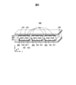
- FIG. 1 is a plan view of the electric circuit body 400 according to the present embodiment
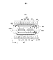
- FIG. 2 is a cross-sectional view taken along the line XX shown in FIG. 1 of the electric circuit body 400
- FIG. 3 is a cross-sectional view taken along the line YY shown in FIG. 1 of the electric circuit body 400.
- the electric circuit body 400 includes three power modules 300 and a cooling member 340.
- the power module 300 has a function of converting a direct current and an alternating current by using a semiconductor element, and generates heat when energized. Therefore, the structure is such that the refrigerant flows through the cooling member 340 to cool the cooling member.
- the refrigerant water or an antifreeze solution in which ethylene glycol is mixed with water is used.
- the cooling member 340 may have a structure in which pin-shaped fins are erected on the base plate of the cooling member 340.
- the cooling member 340 is preferably made of a lightweight aluminum material having high thermal conductivity.
- the cooling member 340 is manufactured by extrusion molding, forging, brazing, or the like.
- the power module 300 includes a positive electrode side terminal 315B and a negative electrode side terminal 319B connected to a capacitor module 500 (see FIG. 14 described later) of a DC circuit on one side.
- a power terminal through which a large current flows such as an AC side terminal 320B connected to the motor generators 192 and 194 of the AC circuit (see FIG. 14 described later), is provided.
- control of power modules such as a lower arm gate signal terminal 325L, a mirror emitter signal terminal 325M, a Kelvin emitter signal terminal 325K, an upper arm gate signal terminal 325U, a mirror emitter signal terminal 325M, and a Kelvin emitter signal terminal 325K. It is equipped with a signal terminal and the like used for.
- an active element 155 and a diode 156 are provided as the first power semiconductor element forming the upper arm circuit.
- the semiconductor material constituting the active element 155 for example, Si, SiC, GaN, GaO, C or the like can be used.
- the diode 156 may be omitted.
- the collector side of the active element 155 and the cathode side of the diode 156 are joined to the second conductor plate 431.
- a first conductor plate 430 is bonded to the emitter side of the active element 155 and the anode side of the diode 156. Solder may be used for these joinings, or sintered metal may be used.
- the first conductor plate 430 and the second conductor plate 431 are not particularly limited as long as they are materials having high electrical conductivity and thermal conductivity, but copper-based or aluminum-based materials are desirable. These may be used alone, or may be plated with Ni, Ag, or the like in order to improve the bondability with solder or a sintered metal.
- the first conductor plate 430 has a recess on the outer periphery of a region connected to the first power semiconductor element 155 and 156 in order to secure an insulation distance (see FIG. 4 described later for details).
- the cooling member 340 is brought into close contact with the first conductor plate 430 via the first sheet-shaped member 440 and the heat conductive member 453.
- the first sheet-shaped member 440 is formed by laminating a first resin insulating layer 442 and a metal foil 444, and the metal foil 444 side is brought into close contact with the heat conductive member 453.
- the cooling member 340 is brought into close contact with the second conductor plate 431 via the second sheet-shaped member 441 and the heat conductive member 453.
- the second sheet-shaped member 441 is formed by laminating a second resin insulating layer 443 and a metal foil 444, and the metal foil 444 side is brought into close contact with the heat conductive member 453.
- an active element 157 and a diode 158 are provided as the second power semiconductor element forming the lower arm circuit.
- the diode 158 is arranged on the back side of the active element 157 in the X-axis direction.
- the collector side of the active element 157 and the cathode side of the diode 158 are joined to the fourth conductor plate 433.
- a third conductor plate 432 is bonded to the emitter side of the active element 157 and the anode side of the diode 158.
- the first sheet-shaped member 440 and the second sheet-shaped member 441 include an embedded portion C covered with a sealing material 360, a first conductor plate 430, and a second conductor. It has a heat radiating surface portion A that overlaps the surface of the plate 431 and a margin portion B that is a region between the buried portion C and the heat radiating surface portion A, and the margin portion B is an electric circuit body 400 rather than the heat radiating surface portion A.
- the buried portion C is retracted to the inside of the electric circuit body 400 (Z-axis direction) from the margin portion B.
- the heat conductive member 453 is not particularly limited as long as it is a material having high thermal conductivity, but it is preferable to use a high heat conductive material such as a metal, ceramics, or carbon-based material in combination with a resin material. This is because the resin material fills the space between the heat conductive member 453 and the cooling member 340 and between the heat conductive member 453 and the sheet-shaped members 440 and 441 to reduce the contact thermal resistance.
- the first power semiconductor element 155, 156, the second power semiconductor element 157, 158, each conductor plate 430, 431, 432, 433, and each sheet-shaped member 440, 441 are sealed with a sealing material 360 by transfer molding. ing.
- the first resin insulating layer 442 and the second resin insulating layer 443 of the sheet-shaped members 440 and 441 are not particularly limited as long as they have adhesiveness to the conductor plates 430, 431, 432, and 433, but are in the form of powder.
- An epoxy resin-based resin insulating layer in which the above-mentioned inorganic filler is dispersed is desirable. This is because the adhesiveness and heat dissipation are well-balanced.
- Each of the sheet-shaped members 440 and 441 may be a single resin insulating layer, but it is desirable to provide a metal foil 444 on the side in contact with the heat conductive member 453.
- a release sheet is provided on the contact surface between the sheet-shaped members 440 and 441 and the mold in order to prevent adhesion to the mold.
- a metal foil 444 is provided. Since the release sheet has poor thermal conductivity, a step of peeling off after transfer molding is required, but in the case of metal leaf 444, transfer can be performed by selecting a copper-based or aluminum-based metal with high thermal conductivity. It can be used without peeling after molding.
- the sealing material 360 which has the effect of improving the reliability of the product.
- FIG. 4 is a cross-sectional perspective view of the power module 300 in the X-ray line shown in FIG. 1, showing a state in which the cooling member 340 is removed from the electric circuit body 400.
- the first sheet-shaped member 440 has a buried portion C covered with a sealing material 360, a heat radiating surface portion A which is a region overlapping the surface of the first conductor plate 430, and the buried portion C and heat dissipation. It has a margin portion B, which is an area between the surface portion A, and the margin portion B recedes into the power module 300 from the heat radiation surface portion A, and the buried portion C is inside the power module 300 rather than the margin portion B. Is retreating to.
- 5 (a) to 5 (c) and 6 (d) to 6 (f) are cross-sectional views showing a method of manufacturing the electric circuit body 400.
- the left side of each figure shows a cross-sectional view of one power module on the X-ray line shown in FIG. 1, and the right side shows a cross-sectional view of one power module on the YY line shown in FIG.
- FIG. 5A is a diagram showing a solder connecting process and a wire bonding process.
- the collector side of the active element 155 which is the first power semiconductor element, and the cathode side of the diode 156 are connected to the second conductor plate 431, and the gate electrode of the active element 155 is connected by wire bonding.
- the emitter side of the active element 155 and the anode side of the diode 156 are connected to the first conductor plate 430.
- the collector side of the active element 157 which is the second power semiconductor element, and the cathode side of the diode 158 are connected to the fourth conductor plate 433, and the gate electrode of the active element 157 is connected by wire bonding.
- the emitter side of the active element 157 and the anode side of the diode 158 are connected to the third conductor plate 432.
- FIG. 5B is a diagram showing a mold installation process.
- the transfer mold device 601 vacuum attracts the spring 602 and the sheet-shaped members 440 and 441 to the mold.
- the vacuum degassing mechanism for vacuum-sucking the sheet-shaped members 440 and 441 to the mold is not shown.
- Sheet-shaped members 440 and 441 aligned in advance using a jig are held by vacuum suction in a mold heated to a constant temperature of 175 ° C.
- a circuit body 310 preheated to 175 ° C. in advance is installed therein in a mold in a state separated from the sheet-shaped members 440 and 441.
- FIG. 5C is a diagram showing a transfer molding process. From the state where the sheet-shaped members 440 and 441 and the circuit body 310 are separated from each other, the upper and lower molds are brought close to each other, and only the packings installed around the upper and lower molds (not shown) are brought into contact with each other. Next, the inside of the mold cavity is evacuated. When the vacuum exhaust is completed so that the pressure drops below the predetermined pressure, the upper and lower molds are completely tightened so as to further crush the packing. At this time, the sheet-shaped members 440 and 441 come into contact with the circuit body 310.
- the sheet-shaped members 440 and 441 and the circuit body 310 come into contact with each other and are brought into close contact with each other by the pressure applied by the spring 602, so that the voids can be brought into close contact with each other without being involved.
- the sealing material 360 is injected into the cavity of the mold.
- the heat radiating surface portion A and the margin portion B are on the same surface and do not recede inward, and the buried portion C has a shape in which the heat radiating surface portion A and the margin portion B recede inward. That is, in this step, the buried portion C recedes inward from the heat radiating surface portion A and the margin portion B, and is sealed with the sealing material 360.
- the heat radiating surface portion A and the margin portion B are on the same surface and do not recede inward, and the buried portion C recedes inward to seal.
- FIG. 6 (d) is a diagram showing a curing process.
- the power module 300 sealed with the sealing material 360 is taken out from the transfer molding apparatus 601, cooled at room temperature, and cured for 2 hours or more.
- the margin portion B recedes from the heat radiating surface portion A into the inside of the power module 300 due to the curing shrinkage and the cooling shrinkage of the sealing material 360.
- the buried portion C recedes from the margin portion B into the inside of the power module 300.
- the power module 300 includes a positive electrode side terminal 315B and a negative electrode side terminal 319B connected to a capacitor module 500 (see FIG. 14 described later) on one side in the X-axis direction, and a motor generator of an AC circuit on the other side.
- the amount of the sealing material 360 increases at both ends of the power module 300 in the X-axis direction, and the margin portion B is retracted from the heat radiating surface portion A to the inside of the power module 300 due to the curing shrinkage and the cooling shrinkage of the sealing material 360. The effect is more pronounced.
- FIG. 6E is a diagram showing an installation process of the cooling member 340.
- the cooling member 340 is pressed against both sides of the power module 300 via the heat conductive member 453.
- the cooling member 340 is brought into close contact with the first sheet-shaped member 440 and the second sheet-shaped member 441 via the heat conductive member 453.
- FIG. 6 (f) is a diagram showing an electric circuit body 400 manufactured by the above steps. In this way, the cooling members 340 are installed on both sides of the power module 300 to manufacture the electric circuit body 400.
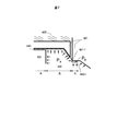
- FIG. 7 is a diagram showing the vicinity of the end portion of the first sheet-shaped member 440 in the transfer molding process shown in FIG. 5 (c).
- the first sheet-shaped member 440 is shown by a broken line.
- the first sheet-shaped member 440 is pressed by the transfer molding device 601 on the first conductor plate 430. Then, it is sealed with a sealing material 360.
- the end portion of the sheet-shaped member 440 is covered with the sealing material 360 in the buried portion C. Then, in the buried portion C, the resin burr composed of the sealing material 360 and the resin component of the sealing material 360 is stopped from flowing into the margin portion B between the sheet-shaped member 440 and the mold.
- the sheet-shaped member 440 is vacuum-sucked to the mold of the transfer molding device 601 but its suction force is much smaller than the molding pressure Pa for injecting the sealing material 360. Further, when the inside of the mold into which the sealing material 360 is injected is exhausted due to vacuum forming, the suction force is further weakened. Therefore, between the sheet-shaped member 440 and the mold of the transfer molding device 601, a sealing material 360 and a resin burr composed of a resin component in the sealing material 360 are formed on the outer peripheral portion (end) of the sheet-shaped member 440. It flows in from 440-1.
- the convex portion 601-1 is used as the sealing material 360. And resin burrs stop.
- the sealing material 360 and the resin burr stop at the convex portion 601-1 will be described.
- the molding pressure Pa generated by the flowing sealing material 360 presses the sheet-shaped member 440 against the mold, and then the inside of the mold is pressed.
- a final molding pressure Pa which is one step higher than before, is applied to the sealing material 360 as a hydrostatic pressure.
- the sealing material 360 also flows into a minute gap, and the sealing material 360 and the resin burr are formed in the narrow gap between the sheet-shaped member 440 and the mold from the outer peripheral portion (end) 440-1 of the sheet-shaped member 440. Inflow.
- the molding pressure Pa that tries to press the sheet-shaped member 440 against the mold causes the sealing material 360 to flow into the narrow gap between the sheet-shaped member 440 and the mold. Since it completely antagonizes the pressure Pb to be tried, it acts extremely effectively in stopping the sealing material 360 and the resin burr. In this way, in the buried portion C, the outer peripheral portion (end portion) 440-1 of the sheet-shaped member 440 is covered with the sealing material 360 and the resin burr.
- the margin portion B is retracted inward from the heat radiation surface portion A, and the buried portion C is retracted inward from the margin portion B. Therefore, details will be described later. Even if the electric circuit body 400 is warped, the heat radiating surface portion A can be pressed against the cooling member 340 with a high surface pressure.
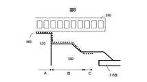
- FIG. 8 is a modification 1, and is a diagram showing details of the vicinity of the end portion of the first sheet-shaped member 440.
- the first sheet-shaped member 440 is shown by a broken line.
- the first sheet-shaped member 440 is arranged between the first conductor plate 430 and the cooling member 340.
- the margin portion B is retracted inward from the heat radiating surface portion A, and the buried portion C is retracted inward from the margin portion B.
- the margin portion B suddenly recedes inward from the heat radiation surface portion A due to the curing step, but such a shape may be used.
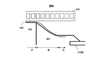
- FIG. 9 is a modification 2 and is a diagram showing details of the vicinity of the end portion of the first sheet-shaped member 440.
- the first sheet-shaped member 440 is shown by a broken line.
- the first sheet-shaped member 440 is arranged between the first conductor plate 430 and the cooling member 340.
- the margin portion B is retracted inward from the heat radiating surface portion A, and the buried portion C is retracted inward from the margin portion B.
- this modification 2 an example is shown in which the margin portion B gradually recedes inward as it moves away from the heat radiation surface portion A due to the curing step, but such a shape may be used.
- the margin portion B may be retracted inward from the heat radiating surface portion A, and the buried portion C may be retracted inward from the margin portion B. Although omitted, a groove may be formed in the margin B.
- FIG. 10 is a diagram showing the relationship between the shrinkage amount of the sealing material 360 and the temperature.
- the horizontal axis shows the temperature and the vertical axis shows the amount of shrinkage.
- the sealing material 360 is injected into the mold of the transfer molding apparatus 601. Pay attention to the contraction of the constituent members of the power module 300 in the Z-axis direction based on the dimensions immediately after injection. Looking at the constituent members from the emitter side to the collector side of the active elements 155 and 157 of the power module 300, the first sheet-shaped member 440, the first conductor plate 430 and the third conductor plate 432, the solder, and the first power The semiconductor elements 155, 156, the second power semiconductor element 157, 158, the solder, the second conductor plate 431 and the fourth conductor plate 433, and the second sheet-like member 441.
- Each of the sheet-shaped members 440 and 441 is formed by laminating a resin insulating layer having a thickness of 100 um to 500 um and a metal foil having a thickness of 30 um to 200 um.
- Each conductor plate 430, 431 is composed of a copper-based material having a thickness of 1 mm to 5 mm.
- Solder is composed of tin-based materials with a thickness of 50um to 200um.
- the first power semiconductor device 155, 156 and the second power semiconductor device 157, 158 are made of a silicon-based material having a thickness of 80 um to 200 um.
- the amount of shrinkage in the Z-axis direction of each of these constituent members is approximated by the amount of heat shrinkage of pure copper, representing the copper-based material which is the thickest constituent material.
- the encapsulant 360 is injected into the mold of the transfer molding apparatus 601 and then cured and shrunk as the curing reaction progresses.
- the amount of curing shrinkage varies depending on the composition of the encapsulant 360. It varies depending on the proportion of the epoxy resin component that undergoes a curing reaction and the proportion of other fillers that do not undergo a curing reaction. The greater the proportion of the epoxy resin component, the greater the amount of curing shrinkage.
- the power module 300 taken out from the mold of the transfer molding apparatus 601 is cooled to room temperature.
- the glass transition temperatures ⁇ t and ⁇ t are lower than Tmold, as in the sealing materials ⁇ and ⁇ shown in FIG. 10, the glass transition temperatures ⁇ t and ⁇ t are shrunk with a large shrinkage amount, and the glass transition temperatures ⁇ t and ⁇ t are contracted to the glass transition temperatures ⁇ t and ⁇ t, respectively.
- the temperature becomes lower the glass shrinks with a smaller amount of shrinkage.
- T1 is the minimum value of the operating environment temperature of the power module 300
- T2 is the maximum value of the operating environment temperature.
- T1 is ⁇ 40 ° C.
- T2 is 125 ° C.
- the shrinkage amount is larger than that of copper Cu
- the shrinkage amount of the sealing material 360 is in the hatching region H shown in FIG. 10
- the margin B dissipates heat. It recedes inward from the surface A.
- the sealing materials ⁇ and ⁇ correspond to this, and the sealing material 360 used in the present embodiment is used.
- the sealing material ⁇ is, for example, a polyfunctional epoxy resin (silica filler 66% by volume).
- the sealing material ⁇ is, for example, a novolak type epoxy resin (silica filler 66% by volume).
- the sealing material ⁇ does not correspond to the sealing material 360 used in the present embodiment because the heat radiating surface portion A recedes inward from the margin portion B.
- the difference in the amount of shrinkage between the sealing material 360 and Cu recedes inside the electric circuit body 400 in the Z-axis direction. That is, the sealing material 360 has a larger amount of shrinkage with respect to temperature than the first conductor plate 430, the second conductor plate 431, the third conductor plate 432, and the fourth conductor plate 433. Therefore, in the normal operating temperature range, the margin portion B and the buried portion C recede into the inside of the electric circuit body 400 from the heat radiation surface portion A. Further, the difference in the amount of shrinkage between the sealing material 360 and Cu is warpage in the XY direction.
- the volume of the second conductor plate 431 and the fourth conductor plate 433 on the collector side of the electric circuit body 400 is larger than that of the first conductor plate 430 and the third conductor plate 432 on the emitter side.
- the shrinkage amount of the sealing material 360 is larger than Cu, the sealing material 360 shrinks more than Cu. Comparing the collector side and the emitter side, the emitter side, which occupies a large proportion of the sealing material 360, contracts more than the collector side, so that a warp occurs in which the emitter side becomes concave.
- FIG. 11 (a) is a schematic cross-sectional view of the electric circuit body 400 according to the present embodiment
- FIG. 11 (b) is a schematic cross-sectional view of Comparative Example 1
- FIG. 11 (c) is a schematic cross-sectional view of Comparative Example 2. be. In each case, the case where the warp Q in which the emitter side is concave occurs is shown.
- the margin portion B is retracted inward from the heat radiating surface portion A, and the buried portion C is retracted inward from the margin portion B. Therefore, the electric circuit body 400 Even if the warp Q occurs, the heat radiating surface portion A is in close contact with the cooling member 340 without the end portion of the sealing material 360 coming into contact with the cooling member 340. Therefore, there is an effect of excellent heat dissipation.
- the warp Q of the electric circuit body 400 is remarkable in the X-axis direction of the electric circuit body 400, but the amount of the sealing material 360 increases at both ends of the electric circuit body 400 in the X-axis direction, and the sealing material 360 There is an effect that the margin portion B is retracted from the heat radiation surface portion A to the inside of the power module 300 by the curing shrinkage and the cooling shrinkage of the above.
- FIG. 12 is a translucent plan view of the power module 300 according to the present embodiment.
- FIG. 13 is a circuit diagram of the power module 300 in this embodiment.
- the positive electrode side terminal 315B outputs from the collector side of the upper arm circuit and is connected to the positive electrode side of the battery or the capacitor.
- the upper arm gate signal terminal 325U outputs from the gate and emitter sense of the active element 155 of the upper arm circuit.
- the negative electrode side terminal 319B outputs from the emitter side of the lower arm circuit, and is connected to the negative electrode side of the battery or capacitor, or GND.
- the lower arm gate signal terminal 325L outputs from the gate and emitter sense of the active element 157 of the lower arm circuit.
- the AC side terminal 320B outputs from the collector side of the lower arm circuit and is connected to the motor. When grounding the neutral point, the lower arm circuit is connected to the negative electrode side of the capacitor instead of GND.
- first conductor plate (upper arm circuit emitter side) 430 and the second conductor plate (upper arm circuit collector side) 431 are arranged above and below the active element 155 and the diode 156 of the first power semiconductor element (upper arm circuit).
- a third conductor plate (lower arm circuit emitter side) 432 and a fourth conductor plate (lower arm circuit collector side) 433 are arranged above and below the active element 157 and the diode 158 of the second power semiconductor element (lower arm circuit).
- the power module 300 of this embodiment has a 2in1 structure in which two arm circuits, an upper arm circuit and a lower arm circuit, are integrated into one module.
- a structure in which a plurality of upper arm circuits and lower arm circuits are integrated into one module may be used. In this case, the number of output terminals from the power module 300 can be reduced to reduce the size.
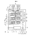
- FIG. 14 is a circuit diagram of the power conversion device 200 using the electric circuit body 400.
- the power conversion device 200 includes inverter circuits 140 and 142, an inverter circuit 43 for auxiliary equipment, and a capacitor module 500.
- the inverter circuits 140 and 142 are composed of an electric circuit body 400 (not shown) including a plurality of power modules 300, and a three-phase bridge circuit is formed by connecting them.
- the power module 300 is further connected in parallel, and these parallel connections are made corresponding to each phase of the three-phase inverter circuit, so that the increase in current capacity can be dealt with. Further, the increase in current capacity can be coped with by connecting the active elements 155, 157 and the diodes 156, 158, which are power semiconductor elements built in the power module 300, in parallel.
- the inverter circuit 140 and the inverter circuit 142 have the same basic circuit configuration, and the control method and operation are basically the same. Since the outline of the circuit-like operation of the inverter circuit 140 and the like is well known, detailed description thereof will be omitted here.
- the upper arm circuit includes an active element 155 for the upper arm and a diode 156 for the upper arm as a power semiconductor element for switching
- the lower arm circuit is a lower power semiconductor element for switching. It includes an active element 157 for the arm and a diode 158 for the lower arm.
- the active elements 155 and 157 receive a drive signal output from one or the other of the two driver circuits constituting the driver circuit 174 and perform a switching operation to convert the DC power supplied from the battery 136 into three-phase AC power. ..
- the active element 155 for the upper arm and the active element 157 for the lower arm include a collector electrode, an emitter electrode, and a gate electrode.
- the diode 156 for the upper arm and the diode 158 for the lower arm include two electrodes, a cathode electrode and an anode electrode. As shown in FIG. 13, the cathode electrodes of the diodes 156 and 158 are electrically connected to the collector electrodes of the active elements 155 and 157, and the anode electrodes are electrically connected to the emitter electrodes of the active elements 155 and 157. As a result, the current flow from the emitter electrode to the collector electrode of the active element 155 for the upper arm and the active element 157 for the lower arm is in the forward direction.
- a MOSFET metal oxide semiconductor type field effect transistor
- the diode 156 for the upper arm and the diode 158 for the lower arm are unnecessary.
- the positive electrode side terminal 315B and the negative electrode side terminal 319B of each of the upper and lower arm series circuits are connected to the DC terminals 362A and 362B for connecting the capacitors of the capacitor module 500, respectively.
- AC power is generated at the connection between the upper arm circuit and the lower arm circuit, respectively, and the connection between the upper arm circuit and the lower arm circuit of each of the upper and lower arm series circuits is connected to the AC side terminal 320B of each power module 300.
- the AC side terminal 320B of each power module 300 of each phase is connected to the AC output terminal of the power converter 200, and the generated AC power is supplied to the stator winding of the motor generator 192 or 194.
- the control circuit 172 controls the switching timing of the active element 155 for the upper arm and the active element 157 of the lower arm based on the input information from the control device or the sensor (for example, the current sensor 180) on the vehicle side. Generate a timing signal.
- the driver circuit 174 generates a drive signal for switching the active element 155 for the upper arm and the active element 157 for the lower arm based on the timing signal output from the control circuit 172.
- 181 and 182, 188 are connectors.
- the upper / lower arm series circuit includes a temperature sensor (not shown), and the temperature information of the upper / lower arm series circuit is input to the control circuit 172. Further, voltage information on the DC positive electrode side of the upper / lower arm series circuit is input to the control circuit 172.
- the control circuit 172 performs overtemperature detection and overvoltage detection based on the information, and when overtemperature or overvoltage is detected, switching of all the active elements 155 for the upper arm and the active element 157 for the lower arm. Stop the operation and protect the upper / lower arm series circuit from overtemperature or overvoltage.
- the power conversion device 200 includes a housing 12 composed of a lower case 11 and an upper case 10 and formed in a substantially rectangular parallelepiped shape.
- An electric circuit body 400, a capacitor module 500, and the like are housed inside the housing 12.
- the electric circuit body 400 has a cooling flow path, and a cooling water inflow pipe 13 and a cooling water outflow pipe 14 communicating with the cooling flow path project from one side surface of the housing 12.
- the lower case 11 is opened on the upper side (Z direction), and the upper case 10 is attached to the lower case 11 by closing the opening of the lower case 11.
- the upper case 10 and the lower case 11 are formed of an aluminum alloy or the like, and are sealed and fixed to the outside.
- the upper case 10 and the lower case 11 may be integrated. Since the housing 12 has a simple rectangular parallelepiped shape, it can be easily attached to a vehicle or the like, and productivity is also improved.
- a connector 17 is attached to one side surface of the housing 12 in the longitudinal direction, and an AC terminal 18 is connected to this connector 17. Further, a connector 21 is provided on the surface from which the cooling water inflow pipe 13 and the cooling water outflow pipe 14 are led out.
- the electric circuit body 400 is housed in the housing 12.
- a control circuit 172 and a driver circuit 174 are arranged above the electric circuit body 400, and a capacitor module 500 is housed on the DC terminal side of the electric circuit body 400.
- the AC side terminal 320B of the electric circuit body 400 penetrates the current sensor 180 and is joined to the bus bar.
- the positive electrode side terminal 315B and the negative electrode side terminal 319B which are the DC terminals of the electric circuit body 400, are joined to the positive and negative electrode terminals (DC terminals 362A and 362B in FIG. 13) of the capacitor module 500, respectively.
- the electric circuit body 400 has a power semiconductor element 155, a first conductor plate 430 connected to one surface of the power semiconductor element 155, and a first resin insulating layer 442, and is formed of the first conductor plate 430.
- the first sheet-shaped member 440 that covers at least the surface, the sealing material 360 that seals the ends of the power semiconductor element 155, the first conductor plate 430, and the first sheet-shaped member 440, and the first sheet-shaped member 440.
- the first sheet-shaped member 440 includes a first cooling member 340 that is in close contact with the first sheet-shaped member 440, and the first sheet-shaped member 440 has a buried portion C in which the end portion of the first sheet-shaped member 440 is covered with a sealing material 360, and the surface of the first conductor plate 430. It has a heat-dissipating surface portion A which is an overlapping region and a margin portion B which is a region between the buried portion C and the heat-dissipating surface portion A. It recedes inward from the margin B. As a result, even if the electric circuit body is warped, the adhesion between the electric circuit body and the cooling member is ensured, and the heat dissipation property is not impaired.
- the method for manufacturing the electric circuit body 400 includes a power semiconductor element 155, a first conductor plate 430 connected to one surface of the power semiconductor element 155, and a first resin insulating layer 442, and the first conductor.
- the end portion of the first sheet-shaped member 440 of the first sheet-shaped member 440 is the sealing material 360. It has a buried portion C covered with, a heat radiating surface portion A which is a region overlapping the surface of the first conductor plate 430, and a margin portion B which is a region between the buried portion C and the heat radiating surface portion A.
Landscapes
- Engineering & Computer Science (AREA)
- Power Engineering (AREA)
- Cooling Or The Like Of Semiconductors Or Solid State Devices (AREA)
- Structures Or Materials For Encapsulating Or Coating Semiconductor Devices Or Solid State Devices (AREA)
- Encapsulation Of And Coatings For Semiconductor Or Solid State Devices (AREA)
- Inverter Devices (AREA)
Abstract
パワー半導体素子と、前記パワー半導体素子の一方の面に接続される第1導体板と、第1樹脂絶縁層を有し、前記第1導体板の表面を少なくとも覆う第1シート状部材と、前記パワー半導体素子、前記第1導体板、および前記第1シート状部材の端部を封止する封止材と、前記第1シート状部材に密着する第1冷却部材とを備え、前記第1シート状部材は、前記第1シート状部材の前記端部が前記封止材によって覆われた埋没部と、前記第1導体板の表面と重なる領域である放熱面部と、前記埋没部と前記放熱面部との間の領域である余白部と、を有し、前記余白部は前記放熱面部よりも内部に後退し、前記埋没部は前記余白部よりも内部に後退している電気回路体。
Description
本発明は、電気回路体、電力変換装置、および電気回路体の製造方法に関する。
パワー半導体素子のスイッチングを用いた電力変換装置は、変換効率が高いため、民生用、車載用、鉄道用、変電設備等に幅広く利用されている。このパワー半導体素子は通電により発熱するため、高い放熱性が求められる。例えば、車載用においては、小型、軽量化のため水冷を用いた高効率な装置が採用されている。
特許文献1には、半導体素子とヒートシンクとを封止しているモールド樹脂は、放熱面を囲う位置に凹部が設けられており、絶縁シートは、放熱面の全体を覆いつつ、端部が凹部内に接着されている電気回路体が開示されている。
特許文献1に記載の装置の放熱面に冷却部材を密着した場合に、電気回路体に反りが生じると冷却部材との間の密着性が弱まり、放熱性が損なわれる。
本発明による電気回路体は、パワー半導体素子と、前記パワー半導体素子の一方の面に接続される第1導体板と、第1樹脂絶縁層を有し、前記第1導体板の表面を少なくとも覆う第1シート状部材と、前記パワー半導体素子、前記第1導体板、および前記第1シート状部材の端部を封止する封止材と、前記第1シート状部材に密着する第1冷却部材とを備え、前記第1シート状部材は、前記第1シート状部材の前記端部が前記封止材によって覆われた埋没部と、前記第1導体板の表面と重なる領域である放熱面部と、前記埋没部と前記放熱面部との間の領域である余白部と、を有し、前記余白部は前記放熱面部よりも内部に後退し、前記埋没部は前記余白部よりも内部に後退している。
本発明による電気回路体の製造方法は、パワー半導体素子と、前記パワー半導体素子の一方の面に接続される第1導体板と、第1樹脂絶縁層を有し、前記第1導体板の表面を少なくとも覆う第1シート状部材とを封止材で封止する工程であって、前記第1シート状部材は、前記第1シート状部材の端部が前記封止材によって覆われる埋没部と、前記第1導体板の表面と重なる領域である放熱面部と、前記埋没部と前記放熱面部との間の領域である余白部と、を有し、前記埋没部を、前記放熱面部および前記余白部よりも内部に後退して、前記封止材で封止する第1工程と、前記封止材を硬化収縮させ、前記余白部を前記放熱面部より内部に後退させる第2工程と、冷却部材を前記第1シート状部材に密着する第3工程と、よりなる。
本発明による電気回路体の製造方法は、パワー半導体素子と、前記パワー半導体素子の一方の面に接続される第1導体板と、第1樹脂絶縁層を有し、前記第1導体板の表面を少なくとも覆う第1シート状部材とを封止材で封止する工程であって、前記第1シート状部材は、前記第1シート状部材の端部が前記封止材によって覆われる埋没部と、前記第1導体板の表面と重なる領域である放熱面部と、前記埋没部と前記放熱面部との間の領域である余白部と、を有し、前記埋没部を、前記放熱面部および前記余白部よりも内部に後退して、前記封止材で封止する第1工程と、前記封止材を硬化収縮させ、前記余白部を前記放熱面部より内部に後退させる第2工程と、冷却部材を前記第1シート状部材に密着する第3工程と、よりなる。
本発明によれば、電気回路体に反りが生じても、冷却部材との間の密着性を確保し、放熱性が損なわれない。
以下、図面を参照して本発明の実施形態を説明する。以下の記載および図面は、本発明を説明するための例示であって、説明の明確化のため、適宜、省略および簡略化がなされている。本発明は、他の種々の形態でも実施する事が可能である。特に限定しない限り、各構成要素は単数でも複数でも構わない。
図面において示す各構成要素の位置、大きさ、形状、範囲などは、発明の理解を容易にするため、実際の位置、大きさ、形状、範囲などを表していない場合がある。このため、本発明は、必ずしも、図面に開示された位置、大きさ、形状、範囲などに限定されない。
図1は、本実施形態による電気回路体400の平面図、図2は、電気回路体400の図1に示すX-X線の断面図である。図3は、電気回路体400の図1に示すY-Y線の断面図である。
図1に示すように、電気回路体400は、3個のパワーモジュール300と冷却部材340よりなる。パワーモジュール300は、半導体素子を用い直流電流と交流電流とを変換する機能があり、通電により発熱する。このため、冷却部材340の中に冷媒を流通して冷却する構造としている。冷媒には、水や水にエチレングリコールを混入した不凍液等を用いる。なお、冷却部材340は、ピン状のフィンが冷却部材340のベース板に立設された構成であってもよい。冷却部材340は、熱伝導率が高く軽量なアルミ系が望ましい。冷却部材340は、押し出し成型や、鍛造、ろう付け等で作製する。
パワーモジュール300は、一方側に、直流回路のコンデンサモジュール500(後述の図14参照)に連結する正極側端子315Bおよび負極側端子319Bを備えている。
正極側端子315Bおよび負極側端子319Bの他方側には、交流回路のモータジェネレータ192、194(後述の図14参照)に連結する交流側端子320B等の大電流が流れるパワー端子を備えている。また、他方側には、下アームゲート信号端子325L、ミラーエミッタ信号端子325M、ケルビンエミッタ信号端子325K、上アームゲート信号端子325U、ミラーエミッタ信号端子325M、ケルビンエミッタ信号端子325K等のパワーモジュールの制御に用いる信号端子等を備えている。
正極側端子315Bおよび負極側端子319Bの他方側には、交流回路のモータジェネレータ192、194(後述の図14参照)に連結する交流側端子320B等の大電流が流れるパワー端子を備えている。また、他方側には、下アームゲート信号端子325L、ミラーエミッタ信号端子325M、ケルビンエミッタ信号端子325K、上アームゲート信号端子325U、ミラーエミッタ信号端子325M、ケルビンエミッタ信号端子325K等のパワーモジュールの制御に用いる信号端子等を備えている。
図2に示すように、上アーム回路を形成する第1パワー半導体素子として、能動素子155、ダイオード156を備える。能動素子155を構成する半導体材料としては、例えばSi、SiC、GaN、GaO、C等を用いることができる。能動素子155のボディダイオードを用いる場合は、ダイオード156を省略してもよい。能動素子155のコレクタ側およびダイオード156のカソード側は、第2導体板431に接合されている。能動素子155のエミッタ側およびダイオード156のアノード側には第1導体板430が接合されている。これらの接合には、はんだを用いてもよいし、焼結金属を用いてもよい。また、第1導体板430、第2導体板431は、電気伝導性と熱伝導率が高い材料であれば特に限定されないが、銅系又はアルミ系材料が望ましい。これらは、単独で用いてもよいが、はんだや、焼結金属との接合性を高めるためNiやAg等のめっきを施してもよい。第1導体板430は、絶縁距離を確保するため第1パワー半導体素子155、156と接続する領域の外周に凹みを有する(詳細は後述の図4参照)。
第1導体板430には、第1シート状部材440、さらに熱伝導部材453を介して冷却部材340が密着される。第1シート状部材440は、第1樹脂絶縁層442と金属箔444とを積層して構成され、金属箔444側が熱伝導部材453に密着される。
第2導体板431には、第2シート状部材441、さらに熱伝導部材453を介して冷却部材340が密着される。第2シート状部材441は、第2樹脂絶縁層443と金属箔444とを積層して構成され、金属箔444側が熱伝導部材453に密着される。
図3に示すように、下アーム回路を形成する第2パワー半導体素子として、能動素子157、ダイオード158(後述の図12、図13参照)を備える。なお、図3において、ダイオード158はX軸方向で能動素子157の奥側に配置されている。能動素子157のコレクタ側およびダイオード158のカソード側は、第4導体板433に接合されている。能動素子157のエミッタ側およびダイオード158のアノード側には第3導体板432が接合されている。
詳細は後述するが、図2に示すように、第1シート状部材440および第2シート状部材441は、封止材360によって覆われた埋没部Cと、第1導体板430、第2導体板431の表面と重なる領域である放熱面部Aと、埋没部Cと放熱面部Aとの間の領域である余白部Bと、を有し、余白部Bは放熱面部Aよりも電気回路体400の内部(Z軸方向)に後退し、埋没部Cは余白部Bよりも電気回路体400の内部(Z軸方向)に後退している。
図3に示すように、第1導体板430、第2導体板431、第3導体板432、第4導体板433は、電流を通電する役割の他に、第1パワー半導体素子155、156、第2パワー半導体素子157、158が発する熱を冷却部材340に伝熱する伝熱部材としての役割を果たしている。各導体板430、431、432、433と冷却部材340とは電位が異なるため、図2に示すように、各導体板430、431、432、433と冷却部材340との間に第1樹脂絶縁層442を有する第1シート状部材440を介し、第2樹脂絶縁層443を有する第2シート状部材441を介する。各シート状部材440、441と冷却部材340との間には、接触熱抵抗を低減するため熱伝導部材453を有する。
熱伝導部材453は、熱伝導率が高い材料であれば特に限定されないが、金属、セラミックス、炭素系材料等の高熱伝導材料を樹脂材料と組み合わせて用いることが好ましい。
これは、熱伝導部材453と冷却部材340との間、熱伝導部材453と各シート状部材440、441との間を樹脂材料が補填し、接触熱抵抗が低減するためである。
これは、熱伝導部材453と冷却部材340との間、熱伝導部材453と各シート状部材440、441との間を樹脂材料が補填し、接触熱抵抗が低減するためである。
第1パワー半導体素子155、156、第2パワー半導体素子157、158、各導体板430、431、432、433、各シート状部材440、441は、トランスファーモールド成型により封止材360で封止されている。各シート状部材440、441の第1樹脂絶縁層442、第2樹脂絶縁層443は、各導体板430、431、432、433との接着性を有するものであれば特に限定されないが、粉末状の無機充填剤を分散したエポキシ樹脂系樹脂絶縁層が望ましい。これは、接着性と放熱性のバランスが良いためである。各シート状部材440、441は、樹脂絶縁層単体でもよいが、熱伝導部材453と接する側に金属箔444を設けることが望ましい。トランスファーモールド成型工程において、各シート状部材440、441を金型に搭載する際、金型への接着を防ぐため、各シート状部材440、441と金型との接触面には、離型シート又は、金属箔444を設ける。離型シートは、熱伝導率が悪いためトランスファーモールド後に剥離する工程が必要となるが、金属箔444の場合は、銅系や、アルミ系の熱伝導率の高い金属を選択することで、トランスファーモールド後に剥離することなく使用することができる。各シート状部材440、441を含めてトランスファーモールドする事で、各シート状部材440、441の端部が封止材360で被覆されることで製品の信頼性が向上する効果がある。
図4は、図1に示すX-X線におけるパワーモジュール300の断面斜視図であり、電気回路体400から冷却部材340を取り除いた状態を示す。図4に示すように、第1シート状部材440は、封止材360によって覆われた埋没部Cと、第1導体板430の表面と重なる領域である放熱面部Aと、埋没部Cと放熱面部Aとの間の領域である余白部Bと、を有し、余白部Bは放熱面部Aよりもパワーモジュール300の内部に後退し、埋没部Cは余白部Bよりもパワーモジュール300の内部に後退している。これにより、第1シート状部材440上に冷却部材340を密着した場合に、電気回路体400に反りが生じても、冷却部材340との間の密着性を確保し、放熱性が損なわれない。
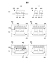
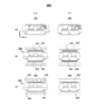
図5(a)~(c)、図6(d)~(f)は、電気回路体400の製造方法を示す断面図である。各図の左側に図1に示すX-X線における1パワーモジュール分の断面図を、右側に図1に示すY-Y線における1パワーモジュール分の断面図を示す。
図5(a)は、はんだ接続工程及びワイヤボンディング工程を示す図である。第2導体板431に、第1パワー半導体素子である能動素子155のコレクタ側およびダイオード156のカソード側を接続し、能動素子155のゲート電極をワイヤボンディングで接続する。第1導体板430に能動素子155のエミッタ側およびダイオード156のアノード側を接続する。同様に、第4導体板433に、第2パワー半導体素子である能動素子157のコレクタ側およびダイオード158のカソード側を接続し、能動素子157のゲート電極をワイヤボンディングで接続する。第3導体板432に能動素子157のエミッタ側およびダイオード158のアノード側を接続する。
図5(b)は、金型設置工程を示す図である。トランスファーモールド装置601は、スプリング602とシート状部材440、441を金型に真空吸着する。シート状部材440、441を金型に真空吸着するための真空脱気機構等は図示省略している。予め175℃の恒温状態に加熱した金型内に、治具を用い位置合わせしたシート状部材440、441を真空吸着にて保持する。そこに、あらかじめ175℃に予熱した回路体310をシート状部材440、441から離間した状態の金型内に設置する。
図5(c)は、トランスファーモールド工程を示す図である。シート状部材440、441と回路体310とが離間した状態から、上下の金型を近接し、図示していない上下金型の周囲に設置したパッキンのみ接触させる。次に、金型のキャビティ内を真空排気する。所定の気圧以下になるよう真空排気が完了すると、パッキンを更に押しつぶすように、上下の金型を完全に締め付ける。この時、シート状部材440、441と回路体310は接触する。真空状態で、シート状部材440、441と回路体310とが接触し、スプリング602による加圧力で密着するため、ボイドを巻き込まず密着することができる。
次に、封止材360を金型のキャビティ内に注入する。トランスファーモールドに用いる金型は、放熱面部Aおよび余白部Bは同一面であり内部に後退しておらず、埋没部Cは放熱面部Aおよび余白部Bよりも内部に後退する形状である。すなわち、この工程において、埋没部Cは、放熱面部Aおよび余白部Bよりも内部に後退して、封止材360で封止する。換言すれば、放熱面部Aおよび余白部Bは同一面であり内部に後退しておらず、埋没部Cが内部に後退して封止する。
図6(d)は、硬化工程を示す図である。トランスファーモールド装置601から封止材360で封止したパワーモジュール300を取り出し、常温で冷却し、2時間以上の硬化を行う。これにより、封止材360の硬化収縮及び冷却収縮によって余白部Bは放熱面部Aよりパワーモジュール300の内部に後退する。埋没部Cは余白部Bよりパワーモジュール300の内部に後退している。特に、パワーモジュール300は、X軸方向の一方側に、コンデンサモジュール500(後述の図14参照)に連結する正極側端子315Bおよび負極側端子319Bを備え、他方側には、交流回路のモータジェネレータ192、194(後述の図14参照)に連結する交流側端子320B等のパワー端子を備えている。このため、パワーモジュール300のX軸方向の両端において封止材360の量が多くなり、封止材360の硬化収縮及び冷却収縮によって余白部Bを放熱面部Aよりパワーモジュール300の内部に後退させる効果がより顕著である。
図6(e)は、冷却部材340の設置工程を示す図である。パワーモジュール300の両面に熱伝導部材453を介して冷却部材340を押し当てる。これにより、冷却部材340は、熱伝導部材453を介して第1シート状部材440、第2シート状部材441に密着される。
図6(f)は、以上の工程により製造された電気回路体400を示す図である。このようにして、パワーモジュール300の両面に冷却部材340が設置されて電気回路体400が製造される。
図6(f)は、以上の工程により製造された電気回路体400を示す図である。このようにして、パワーモジュール300の両面に冷却部材340が設置されて電気回路体400が製造される。
図7は、図5(c)に示したトランスファーモールド工程における第1シート状部材440の端部近傍を示す図である。図7において、第1シート状部材440は破線で示した。第1シート状部材440は第1導体板430上でトランスファーモールド装置601によって押圧されている。そして、封止材360で封止される。
シート状部材440の埋没部Cは余白部Bよりも内部に後退しているので、埋没部Cにおいてシート状部材440の端部が封止材360に被覆される。そして、埋没部Cにおいてシート状部材440と金型との間に封止材360や封止材360の樹脂成分からなる樹脂バリが余白部Bに流入していくのを止める。
シート状部材440はトランスファーモールド装置601の金型に真空吸着しているが、その吸着力は、封止材360を注入する成型圧力Paに比べると遥かに小さい。また、封止材360を注入する金型内部が真空成型のため排気されると、吸着力がさらに弱くなる。このため、シート状部材440とトランスファーモールド装置601の金型の間には、封止材360や、封止材360中の樹脂成分からなる樹脂バリがシート状部材440の外周部(端部)440-1から流入する。この時、シート状部材440の外周部(端部)440-1より少し内側に、凸部601-1が生じるよう金型が加工されていると、この凸部601-1で封止材360や樹脂バリがストップする。
凸部601-1で封止材360や樹脂バリがストップする原理について述べる。図7に示すように、封止材360が金型に流入する過程において、まず、流動する封止材360により生じる成型圧力Paがシート状部材440を金型に押し付け、その後、金型内部がほぼ封止材360で充填された後、これまでより一段大きい最終的な成型圧力Paが封止材360に静水圧として加わる。この時、微小な隙間にも封止材360が流入し、シート状部材440の外周部(端部)440-1からシート状部材440と金型の狭い隙間に封止材360や樹脂バリが流入する。しかし、隙間は狭いので封止材360が流入する圧力Pbに損失が生じる。シート状部材440と金型の隙間に封止材360が流入した先に、凸部601-1があると、シート状部材440と金型の狭い隙間に封止材360が流入しようとする圧力Pbが、シート状部材440を金型に押し付けようとする成型圧力Paと対抗する方向に作用する。この時、シート状部材440を金型に押し付けようとする成型圧力Paの方が、狭い隙間を流動するため圧力Pbより高いため、凸部601-1でシート状部材440と金型との間に流入する封止材360がストップする。特に直角に近い凸部601-1がごく一部でもあると、シート状部材440を金型に押し付けようとする成型圧力Paがシート状部材440と金型の狭い隙間に封止材360が流入しようとする圧力Pbと完全に拮抗するため、封止材360や樹脂バリをストップする上で極めて効果的に作用する。このようにして、埋没部Cではシート状部材440の外周部(端部)440-1が封止材360や樹脂バリにより被覆される。
そして、図6(d)に示した硬化工程により、余白部Bは放熱面部Aよりも内部に後退し、また、埋没部Cは余白部Bよりも内部に後退しているので、詳細は後述するように電気回路体400に反りが生じても高い面圧で放熱面部Aを冷却部材340に押し付けることができる。
図8は、変形例1であり、第1シート状部材440の端部近傍の詳細を示す図である。
図8において、第1シート状部材440は破線で示した。第1シート状部材440は第1導体板430と冷却部材340の間に配置されている。そして、図6(d)に示した硬化工程により、余白部Bは放熱面部Aよりも内部に後退し、また、埋没部Cは余白部Bよりも内部に後退している。この変形例1では、硬化工程により余白部Bが放熱面部Aより急激に内部に後退した例を示すが、このような形状であってもよい。
図8において、第1シート状部材440は破線で示した。第1シート状部材440は第1導体板430と冷却部材340の間に配置されている。そして、図6(d)に示した硬化工程により、余白部Bは放熱面部Aよりも内部に後退し、また、埋没部Cは余白部Bよりも内部に後退している。この変形例1では、硬化工程により余白部Bが放熱面部Aより急激に内部に後退した例を示すが、このような形状であってもよい。
図9は、変形例2であり、第1シート状部材440の端部近傍の詳細を示す図である。
図9において、第1シート状部材440は破線で示した。第1シート状部材440は第1導体板430と冷却部材340の間に配置されている。そして、図6(d)に示した硬化工程により、余白部Bは放熱面部Aよりも内部に後退し、また、埋没部Cは余白部Bよりも内部に後退している。この変形例2では、硬化工程により余白部Bが放熱面部Aから離れるに従って徐々に内部に後退した例を示すが、このような形状であってもよい。
図9において、第1シート状部材440は破線で示した。第1シート状部材440は第1導体板430と冷却部材340の間に配置されている。そして、図6(d)に示した硬化工程により、余白部Bは放熱面部Aよりも内部に後退し、また、埋没部Cは余白部Bよりも内部に後退している。この変形例2では、硬化工程により余白部Bが放熱面部Aから離れるに従って徐々に内部に後退した例を示すが、このような形状であってもよい。
また、変形例1、変形例2の他に、余白部Bは放熱面部Aよりも内部に後退し、また、埋没部Cは余白部Bよりも内部に後退していればよく、例えば、図示省略するが、余白部Bに溝を形成してもよい。
図10は、封止材360の収縮量と温度の関係を示す図である。横軸に温度を、縦軸に収縮量を示す。
例えば温度が175℃のTmoldにおいてトランスファーモールド装置601の金型内に封止材360を注入する。注入直後の寸法を基準にパワーモジュール300の構成部材のZ軸方向の収縮に注目する。パワーモジュール300の能動素子155、157のエミッタ側からコレクタ側に向かって構成部材を見ていくと、第1シート状部材440、第1導体板430および第3導体板432、はんだ、第1パワー半導体素子155、156および第2パワー半導体素子157、158、はんだ、第2導体板431および第4導体板433、第2シート状部材441となる。各シート状部材440、441は、厚さ100umから500umの樹脂絶縁層と、厚さ30umから200umの金属箔とを積層して構成される。各導体板430、431は厚さ1mmから5mmの銅系材料から構成される。はんだは厚さ50umから200umのスズ系材料から構成される。第1パワー半導体素子155、156および第2パワー半導体素子157、158は厚さ80umから200umのシリコン系材料から構成される。
様々な材料から構成されているが、本実施形態では、これらの各構成部材のZ軸方向の収縮量を、最も厚い構成材料である銅系材料を代表し、純銅の熱収縮量で近似して説明する。封止材360は、トランスファーモールド装置601の金型内に注入された後、硬化反応の進行により硬化収縮する。硬化収縮量は、封止材360の組成によって変化する。
硬化反応するエポキシ樹脂成分の割合と、硬化反応しないその他の充填剤の割合により変化し、エポキシ樹脂成分の割合が多い程、硬化収縮量は大きくなる。エポキシ樹脂成分の割合が同じでも、エポキシ樹脂成分中に占める反応性成分であるエポキシ基の割合が大きい程硬化収縮量は大きくなる。トランスファーモールド装置601の金型から取り出されたパワーモジュール300は、常温に冷却される。
硬化反応するエポキシ樹脂成分の割合と、硬化反応しないその他の充填剤の割合により変化し、エポキシ樹脂成分の割合が多い程、硬化収縮量は大きくなる。エポキシ樹脂成分の割合が同じでも、エポキシ樹脂成分中に占める反応性成分であるエポキシ基の割合が大きい程硬化収縮量は大きくなる。トランスファーモールド装置601の金型から取り出されたパワーモジュール300は、常温に冷却される。
図10に示す封止材α、γのように、夫々、ガラス転移温度αt、γtがTmoldより低い場合は、ガラス転移温度αt、γtまでは大きな収縮量で収縮し、ガラス転移温度αt、γtより温度が低くなるとこれより小さい収縮量で収縮する。
図10に示す封止材βのように、ガラス転移温度がTmoldより高い場合は、一定の収縮量で収縮する。T1はパワーモジュール300の使用環境温度の最小値、T2は使用環境温度の最大値で、例えばT1は-40℃、T2は125℃となる。この温度域において、収縮量が銅Cuより大きい場合、つまり、封止材360の収縮量が図10に示すハッチング領域Hに入っている場合、使用温度域T1-T2で、余白部Bは放熱面部Aよりも内部に後退する。封止材β、γがこれに該当し、本実施形態で用いる封止材360となる。封止材βは、例えば、多官能エポキシ樹脂(シリカフィラ66体積%)である。封止材γは、例えば、ノボラック型エポキシ樹脂(シリカフィラ66体積%)である。封止材αは、放熱面部Aが余白部Bより内部に後退するため本実施形態で用いる封止材360に該当しない。
封止材360とCuの収縮量の差は、Z軸方向では電気回路体400の内部に後退する。
すなわち、封止材360は、第1導体板430、第2導体板431、第3導体板432および第4導体板433より温度に対する収縮量が大きい。このため、通常の使用温度域で、余白部B、埋没部Cは放熱面部Aよりも電気回路体400の内部に後退する。
また、封止材360とCuの収縮量の差は、X-Y方向では反りとなる。一般に、電気回路体400は、通常コレクタ側の第2導体板431および第4導体板433の方が、エミッタ側の第1導体板430および第3導体板432よりも体積が大きくなる。封止材360の収縮量がCuより大きい場合、Cuより封止材360の方がより収縮する。コレクタ側とエミッタ側で比較すると、封止材360の占める割合が大きいエミッタ側がコレクタ側より収縮するため、エミッタ側が凹となる反りが発生する。
冷却部材340が片面にある片面冷却構造の電気回路体400の場合、エミッタ側が凹となっても、コレクタ側から放熱するため問題が生じる可能性は少ない。冷却部材340が両面にある両面冷却構造の電気回路体400の場合、エミッタ側が凹となる反りが発生することで、エミッタ側において放熱面部Aと冷却部材340が接する距離が大きくなり放熱性が低下する虞がある。
図11(a)は、本実施形態における電気回路体400の断面模式図、図11(b)は、比較例1の断面模式図、図11(c)は、比較例2の断面模式図である。いずれも、エミッタ側が凹となる反りQが発生した場合を示している。
図11(a)に示すように、本実施形態では、余白部Bは放熱面部Aよりも内部に後退し、埋没部Cは余白部Bよりも内部に後退しているので、電気回路体400に反りQが生じても、封止材360の端部が冷却部材340に当接することなく、放熱面部Aは、冷却部材340に密着している。このため放熱性に優れる効果がある。特に、電気回路体400の反りQは、電気回路体400のX軸方向において顕著であるが、電気回路体400のX軸方向の両端において封止材360の量が多くなり、封止材360の硬化収縮及び冷却収縮によって余白部Bを放熱面部Aよりパワーモジュール300の内部に後退させる効果がある。
一方、図11(b)に示すように、比較例1では、余白部B、埋没部Cは、放熱面部Aよりも内部に後退していない。このため、電気回路体400に反りQが生じた場合に、封止材360の端部が冷却部材340に当接し、このため、冷却部材340と放熱面部Aとの距離が離されて放熱性が悪くなる。
また、図11(c)に示すように、比較例2では、埋没部Cは、余白部Bよりも内部に後退しているが、余白部Bは、放熱面部Aよりも内部に後退していない。このため、電気回路体400に反りQが生じた場合に、余白部Bの端部付近の封止材360が冷却部材340に当接し、このため、冷却部材340と放熱面部Aとの間に隙間が生じ放熱性が悪くなる。
図12は、本実施形態におけるパワーモジュール300の半透過平面図である。図13は、本実施形態におけるパワーモジュール300の回路図である。
図12、図13に示すように、正極側端子315Bは、上アーム回路のコレクタ側から出力しており、バッテリ又はコンデンサの正極側に接続される。上アームゲート信号端子325Uは、上アーム回路の能動素子155のゲート及びエミッタセンスから出力している。負極側端子319Bは、下アーム回路のエミッタ側から出力しており、バッテリ若しくはコンデンサの負極側、又はGNDに接続される。下アームゲート信号端子325Lは、下アーム回路の能動素子157のゲート及びエミッタセンスから出力している。交流側端子320Bは、下アーム回路のコレクタ側から出力しており、モータに接続される。中性点接地をする場合は、下アーム回路は、GNDでなくコンデンサの負極側に接続する。
図12、図13に示すように、正極側端子315Bは、上アーム回路のコレクタ側から出力しており、バッテリ又はコンデンサの正極側に接続される。上アームゲート信号端子325Uは、上アーム回路の能動素子155のゲート及びエミッタセンスから出力している。負極側端子319Bは、下アーム回路のエミッタ側から出力しており、バッテリ若しくはコンデンサの負極側、又はGNDに接続される。下アームゲート信号端子325Lは、下アーム回路の能動素子157のゲート及びエミッタセンスから出力している。交流側端子320Bは、下アーム回路のコレクタ側から出力しており、モータに接続される。中性点接地をする場合は、下アーム回路は、GNDでなくコンデンサの負極側に接続する。
また、第1パワー半導体素子(上アーム回路)の能動素子155およびダイオード156の上下に第1導体板(上アーム回路エミッタ側)430、第2導体板(上アーム回路コレクタ側)431が配置される。第2パワー半導体素子(下アーム回路)の能動素子157およびダイオード158の上下に第3導体板(下アーム回路エミッタ側)432、第4導体板(下アーム回路コレクタ側)433が配置される。
本実施形態のパワーモジュール300は、上アーム回路及び下アーム回路の2つのアーム回路を、1つのモジュールに一体化した構造である2in1構造である。この他に、複数の上アーム回路及び下アーム回路を、1つのモジュールに一体化した構造を用いてもよい。この場合は、パワーモジュール300からの出力端子の数を低減し小型化することができる。
図14は、電気回路体400を用いた電力変換装置200の回路図である。
電力変換装置200は、インバータ回路140、142と、補機用のインバータ回路43と、コンデンサモジュール500とを備えている。インバータ回路140及び142は、パワーモジュール300を複数個備えた電気回路体400(図示省略)により構成されており、それらを接続することにより三相ブリッジ回路を構成している。電流容量が大きい場合には、更にパワーモジュール300を並列接続し、これら並列接続を三相インバータ回路の各相に対応して行うことにより、電流容量の増大に対応できる。また、パワーモジュール300に内蔵しているパワー半導体素子である能動素子155、157やダイオード156、158を並列接続することでも電流容量の増大に対応できる。
電力変換装置200は、インバータ回路140、142と、補機用のインバータ回路43と、コンデンサモジュール500とを備えている。インバータ回路140及び142は、パワーモジュール300を複数個備えた電気回路体400(図示省略)により構成されており、それらを接続することにより三相ブリッジ回路を構成している。電流容量が大きい場合には、更にパワーモジュール300を並列接続し、これら並列接続を三相インバータ回路の各相に対応して行うことにより、電流容量の増大に対応できる。また、パワーモジュール300に内蔵しているパワー半導体素子である能動素子155、157やダイオード156、158を並列接続することでも電流容量の増大に対応できる。
インバータ回路140とインバータ回路142とは、基本的な回路構成は同じであり、制御方法や動作も基本的には同じである。インバータ回路140等の回路的な動作の概要は周知であるため、ここでは詳細な説明を省略する。
上述のように、上アーム回路は、スイッチング用のパワー半導体素子として上アーム用の能動素子155と上アーム用のダイオード156とを備えており、下アーム回路は、スイッチング用のパワー半導体素子として下アーム用の能動素子157と下アーム用のダイオード158とを備えている。能動素子155、157は、ドライバ回路174を構成する2つのドライバ回路の一方あるいは他方から出力された駆動信号を受けてスイッチング動作し、バッテリ136から供給された直流電力を三相交流電力に変換する。
上述したように、上アーム用の能動素子155および下アーム用の能動素子157は、コレクタ電極、エミッタ電極、ゲート電極を備えている。上アーム用のダイオード156および下アーム用のダイオード158は、カソード電極およびアノード電極の2つの電極を備えている。図13に示すように、ダイオード156、158のカソード電極が能動素子155、157のコレクタ電極に、アノード電極が能動素子155、157のエミッタ電極にそれぞれ電気的に接続されている。これにより、上アーム用の能動素子155および下アーム用の能動素子157のエミッタ電極からコレクタ電極に向かう電流の流れが順方向となっている。
なお、能動素子としてはMOSFET(金属酸化物半導体型電界効果トランジスタ)を用いても良く、この場合は、上アーム用のダイオード156、下アーム用のダイオード158は不要となる。
各上・下アーム直列回路の正極側端子315Bと負極側端子319Bとはコンデンサモジュール500のコンデンサ接続用の直流端子362A、362Bにそれぞれ接続されている。上アーム回路と下アーム回路の接続部にはそれぞれ交流電力が発生し、各上・下アーム直列回路の上アーム回路と下アーム回路の接続部は各パワーモジュール300の交流側端子320Bに接続されている。各相の各パワーモジュール300の交流側端子320Bはそれぞれ電力変換装置200の交流出力端子に接続され、発生した交流電力はモータジェネレータ192または194の固定子巻線に供給される。
制御回路172は、車両側の制御装置やセンサ(例えば、電流センサ180)などからの入力情報に基づいて、上アーム用の能動素子155、下アームの能動素子157のスイッチングタイミングを制御するためのタイミング信号を生成する。ドライバ回路174は、制御回路172から出力されたタイミング信号に基づいて、上アーム用の能動素子155、下アーム用の能動素子157をスイッチング動作させるための駆動信号を生成する。
なお、181、182、188はコネクタである。
なお、181、182、188はコネクタである。
上・下アーム直列回路は、不図示の温度センサを含み、上・下アーム直列回路の温度情報が制御回路172に入力される。また、制御回路172には上・下アーム直列回路の直流正極側の電圧情報が入力される。制御回路172は、それらの情報に基づいて過温度検知および過電圧検知を行い、過温度或いは過電圧が検知された場合には全ての上アーム用の能動素子155、下アーム用の能動素子157のスイッチング動作を停止させ、上・下アーム直列回路を過温度或いは過電圧から保護する。
図15は、図14に示す電力変換装置200の外観斜視図であり、図16は、図15に示す電力変換装置200のXV-XV線の断面斜視図である。
図15に示すように、電力変換装置200は、下部ケース11および上部ケース10により構成され、ほぼ直方体形状に形成された筐体12を備えている。筐体12の内部には、電気回路体400、コンデンサモジュール500等が収容されている。電気回路体400は冷却流路を有しており、筐体12の一側面からは、冷却流路に連通する冷却水流入管13および冷却水流出管14が突出している。下部ケース11は、上部側(Z方向)が開口され、上部ケース10は、下部ケース11の開口を塞いで下部ケース11に取り付けられている。上部ケース10と下部ケース11とは、アルミニウム合金等により形成され、外部に対して密封して固定される。上部ケース10と下部ケース11とを一体化して構成してもよい。筐体12を、単純な直方体形状としたことで、車両等への取り付けが容易となり、また、生産性も向上する。
図15に示すように、電力変換装置200は、下部ケース11および上部ケース10により構成され、ほぼ直方体形状に形成された筐体12を備えている。筐体12の内部には、電気回路体400、コンデンサモジュール500等が収容されている。電気回路体400は冷却流路を有しており、筐体12の一側面からは、冷却流路に連通する冷却水流入管13および冷却水流出管14が突出している。下部ケース11は、上部側(Z方向)が開口され、上部ケース10は、下部ケース11の開口を塞いで下部ケース11に取り付けられている。上部ケース10と下部ケース11とは、アルミニウム合金等により形成され、外部に対して密封して固定される。上部ケース10と下部ケース11とを一体化して構成してもよい。筐体12を、単純な直方体形状としたことで、車両等への取り付けが容易となり、また、生産性も向上する。
筐体12の長手方向の一側面に、コネクタ17が取り付けられており、このコネクタ17には、交流ターミナル18が接続されている。また、冷却水流入管13および冷却水流出管14が導出された面には、コネクタ21が設けられている。
図16に示すように、筐体12内には、電気回路体400が収容されている。電気回路体400の上方には、制御回路172およびドライバ回路174が配置され、電気回路体400の直流端子側には、コンデンサモジュール500が収容されている。コンデンサモジュールを電気回路体400と同一高さに配置することで、電力変換装置200を薄型化でき、車両への設置自由度が向上する。電気回路体400の交流側端子320Bは、電流センサ180を貫通してバスバーに接合されている。また、電気回路体400の直流端子である正極側端子315Bおよび負極側端子319Bは、それぞれ、コンデンサモジュール500の正・負極端子(図13の直流端子362A、362B)に接合される。
以上説明した実施形態によれば、次の作用効果が得られる。
(1)電気回路体400は、パワー半導体素子155と、パワー半導体素子155の一方の面に接続される第1導体板430と、第1樹脂絶縁層442を有し、第1導体板430の表面を少なくとも覆う第1シート状部材440と、パワー半導体素子155、第1導体板430、および第1シート状部材440の端部を封止する封止材360と、第1シート状部材440に密着する第1冷却部材340とを備え、第1シート状部材440は、第1シート状部材440の端部が封止材360によって覆われた埋没部Cと、第1導体板430の表面と重なる領域である放熱面部Aと、埋没部Cと放熱面部Aとの間の領域である余白部Bと、を有し、余白部Bは放熱面部Aよりも内部に後退し、埋没部Cは余白部Bよりも内部に後退している。これにより、電気回路体に反りが生じても、冷却部材との間の密着性を確保し、放熱性が損なわれない。
(1)電気回路体400は、パワー半導体素子155と、パワー半導体素子155の一方の面に接続される第1導体板430と、第1樹脂絶縁層442を有し、第1導体板430の表面を少なくとも覆う第1シート状部材440と、パワー半導体素子155、第1導体板430、および第1シート状部材440の端部を封止する封止材360と、第1シート状部材440に密着する第1冷却部材340とを備え、第1シート状部材440は、第1シート状部材440の端部が封止材360によって覆われた埋没部Cと、第1導体板430の表面と重なる領域である放熱面部Aと、埋没部Cと放熱面部Aとの間の領域である余白部Bと、を有し、余白部Bは放熱面部Aよりも内部に後退し、埋没部Cは余白部Bよりも内部に後退している。これにより、電気回路体に反りが生じても、冷却部材との間の密着性を確保し、放熱性が損なわれない。
(2)電気回路体400の製造方法は、パワー半導体素子155と、パワー半導体素子155の一方の面に接続される第1導体板430と、第1樹脂絶縁層442を有し、第1導体板430の表面を少なくとも覆う第1シート状部材440とを封止材360で封止する工程であって、第1シート状部材440は、第1シート状部材440の端部が封止材360によって覆われる埋没部Cと、第1導体板430の表面と重なる領域である放熱面部Aと、埋没部Cと放熱面部Aとの間の領域である余白部Bと、を有し、埋没部Cを、放熱面部Aおよび余白部Bよりも内部に後退して、封止材360で封止する第1工程と、封止材360を硬化収縮させ、余白部Bを放熱面部Aより内部に後退させる第2工程と、冷却部材340を第1シート状部材440に密着する第3工程と、よりなる。これにより、電気回路体に反りが生じても、冷却部材との間の密着性を確保し、放熱性が損なわれない。
本発明は、上記の実施形態に限定されるものではなく、本発明の特徴を損なわない限り、本発明の技術思想の範囲内で考えられるその他の形態についても、本発明の範囲内に含まれる。
10・・・上部ケース、11・・・下部ケース、13・・・冷却水流入管、14・・・冷却水流出管、17・・・コネクタ、18・・・交流ターミナル、21・・・コネクタ、43、140、142・・・インバータ回路、155・・・第1パワー半導体素子(上アーム回路能動素子)、156・・・第1パワー半導体素子(上アーム回路ダイオード)、157・・・第2パワー半導体素子(下アーム回路能動素子)、158・・・第2パワー半導体素子(下アーム回路ダイオード)、172・・・制御回路、174・・・ドライバ回路、180・・・電流センサ、181、182、188・・・コネクタ、192、194・・・モータジェネレータ、200・・・電力変換装置、300・・・パワーモジュール、310・・・回路体、315B・・・正極側端子、319B・・・負極側端子、320B・・・交流側端子、325K・・・ケルビンエミッタ信号端子、325L・・・下アームゲート信号端子、325M・・・ミラーエミッタ信号端子、325U・・・上アームゲート信号端子、340・・・冷却部材、360・・・封止材、400・・・電気回路体、430・・・第1導体板(上アーム回路エミッタ側)、431・・・第2導体板(上アーム回路コレクタ側)、432・・・第3導体板(下アーム回路エミッタ側)、433・・・第4導体板(下アーム回路コレクタ側)、440・・・第1シート状部材(エミッタ側)、441・・・第2シート状部材(コレクタ側)、442・・・第1樹脂絶縁層(エミッタ側)、443・・・第2樹脂絶縁層(コレクタ側)、444・・・金属箔、453・・・熱伝導部材、500・・・コンデンサモジュール、601・・・トランスファーモールド装置、602・・・スプリング、A・・・放熱面部、B・・・余白部、C・・・埋没部。
Claims (12)
- パワー半導体素子と、前記パワー半導体素子の一方の面に接続される第1導体板と、第1樹脂絶縁層を有し、前記第1導体板の表面を少なくとも覆う第1シート状部材と、前記パワー半導体素子、前記第1導体板、および前記第1シート状部材の端部を封止する封止材と、前記第1シート状部材に密着する第1冷却部材とを備え、
前記第1シート状部材は、前記第1シート状部材の前記端部が前記封止材によって覆われた埋没部と、前記第1導体板の表面と重なる領域である放熱面部と、前記埋没部と前記放熱面部との間の領域である余白部と、を有し、前記余白部は前記放熱面部よりも内部に後退し、前記埋没部は前記余白部よりも内部に後退している電気回路体。 - 請求項1に記載の電気回路体において、
前記パワー半導体素子の他方の面に接続される第2導体板と、第2樹脂絶縁層を有し、前記第2導体板の表面を少なくとも覆う第2シート状部材と、前記第2シート状部材に密着する第2冷却部材とを備え、
前記封止材は、前記第2導体板、および前記第2シート状部材の端部を封止し、
前記第2シート状部材は、前記第2シート状部材の前記端部が前記封止材によって覆われた埋没部と、前記第2導体板の表面と重なる領域である放熱面部と、前記埋没部と前記放熱面部との間の領域である余白部と、を有し、前記余白部は前記放熱面部よりも内部に後退し、前記埋没部は前記余白部よりも内部に後退している電気回路体。 - 請求項1に記載の電気回路体において、
前記第1シート状部材は、前記第1樹脂絶縁層と、第1金属箔とを積層してなり、
前記第1冷却部材は、前記第1金属箔を介して前記第1シート状部材の前記放熱面部と密着する電気回路体。 - 請求項2に記載の電気回路体において、
前記第2シート状部材は、前記第2樹脂絶縁層と、第2金属箔とを積層してなり、
前記第2冷却部材は、前記第2金属箔を介して前記第2シート状部材の前記放熱面部と密着する電気回路体。 - 請求項1に記載の電気回路体において、
前記第1冷却部材は、熱伝導部材を介して前記第1シート状部材と密着する電気回路体。 - 請求項2に記載の電気回路体において、
前記第2冷却部材は、熱伝導部材を介して前記第2シート状部材と密着する電気回路体。 - 請求項1または請求項3に記載の電気回路体において、
前記封止材は、前記第1導体板より温度に対する収縮量が大きい電気回路体。 - 請求項2または請求項4に記載の電気回路体において、
前記封止材は、前記第2導体板より温度に対する収縮量が大きい電気回路体。 - 請求項1または請求項2に記載の電気回路体において、
前記パワー半導体素子より導出され、コンデンサに接続される第1端子と、
前記第1端子とは反対側に前記パワー半導体素子より導出され、モータに接続される第2端子とを備えた電気回路体。 - 請求項1から請求項9までのいずれか一項に記載の電気回路体により構成され、直流電力を交流電力に変換する電力変換装置。
- パワー半導体素子と、前記パワー半導体素子の一方の面に接続される第1導体板と、第1樹脂絶縁層を有し、前記第1導体板の表面を少なくとも覆う第1シート状部材とを封止材で封止する工程であって、前記第1シート状部材は、前記第1シート状部材の端部が前記封止材によって覆われる埋没部と、前記第1導体板の表面と重なる領域である放熱面部と、前記埋没部と前記放熱面部との間の領域である余白部と、を有し、前記埋没部を、前記放熱面部および前記余白部よりも内部に後退して、前記封止材で封止する第1工程と、
前記封止材を硬化収縮させ、前記余白部を前記放熱面部より内部に後退させる第2工程と、
冷却部材を前記第1シート状部材に密着する第3工程と、
よりなる電気回路体の製造方法。 - 請求項11に記載の電気回路体の製造方法において、
前記第3工程は、熱伝導部材を介して前記冷却部材を前記第1シート状部材へ密着する工程を含む電気回路体の製造方法。
Priority Applications (3)
| Application Number | Priority Date | Filing Date | Title |
|---|---|---|---|
| US17/910,201 US12506133B2 (en) | 2020-03-09 | 2020-12-25 | Electric circuit body, power conversion device, and method for manufacturing electric circuit body |
| DE112020006116.7T DE112020006116B4 (de) | 2020-03-09 | 2020-12-25 | Körper einer elektrischen schaltung, leistungsumsetzungsvorrichtung und herstellungsverfahren für körper einer elektrischen schaltung |
| CN202080096165.7A CN115088065B (zh) | 2020-03-09 | 2020-12-25 | 电路体、电力转换装置及电路体的制造方法 |
Applications Claiming Priority (2)
| Application Number | Priority Date | Filing Date | Title |
|---|---|---|---|
| JP2020-039863 | 2020-03-09 | ||
| JP2020039863A JP7491707B2 (ja) | 2020-03-09 | 2020-03-09 | 電気回路体、電力変換装置、および電気回路体の製造方法 |
Publications (1)
| Publication Number | Publication Date |
|---|---|
| WO2021181831A1 true WO2021181831A1 (ja) | 2021-09-16 |
Family
ID=77669700
Family Applications (1)
| Application Number | Title | Priority Date | Filing Date |
|---|---|---|---|
| PCT/JP2020/048708 Ceased WO2021181831A1 (ja) | 2020-03-09 | 2020-12-25 | 電気回路体、電力変換装置、および電気回路体の製造方法 |
Country Status (5)
| Country | Link |
|---|---|
| US (1) | US12506133B2 (ja) |
| JP (1) | JP7491707B2 (ja) |
| CN (1) | CN115088065B (ja) |
| DE (1) | DE112020006116B4 (ja) |
| WO (1) | WO2021181831A1 (ja) |
Cited By (4)
| Publication number | Priority date | Publication date | Assignee | Title |
|---|---|---|---|---|
| EP4258346A1 (en) * | 2022-04-06 | 2023-10-11 | Semiconductor Components Industries, LLC | Thermal performance improvement and stress reduction in semiconductor device modules |
| WO2024262388A1 (ja) * | 2023-06-21 | 2024-12-26 | 日立Astemo株式会社 | 半導体モジュール、電気回路体、および電力変換装置 |
| WO2025126546A1 (ja) * | 2023-12-13 | 2025-06-19 | Astemo株式会社 | 半導体モジュール、電力変換装置、半導体モジュールの製造方法 |
| WO2026154838A1 (ja) * | 2025-01-16 | 2026-07-23 | Astemo株式会社 | 半導体装置及びそれを用いた電力変換装置 |
Families Citing this family (8)
| Publication number | Priority date | Publication date | Assignee | Title |
|---|---|---|---|---|
| JP6961784B1 (ja) | 2020-12-28 | 2021-11-05 | 日立Astemo株式会社 | パワー半導体装置 |
| WO2022248068A1 (en) * | 2021-05-28 | 2022-12-01 | Dynex Semiconductor Limited | Semiconductor device |
| JP7580349B2 (ja) * | 2021-07-01 | 2024-11-11 | 日立Astemo株式会社 | パワー半導体装置 |
| JP7690389B2 (ja) * | 2021-12-16 | 2025-06-10 | Astemo株式会社 | 半導体装置及び電力変換装置 |
| JP7734631B2 (ja) * | 2022-07-04 | 2025-09-05 | Astemo株式会社 | 電気回路体および電力変換装置 |
| CN117810183A (zh) * | 2022-09-30 | 2024-04-02 | 力特半导体(无锡)有限公司 | 半导体封装件 |
| CN116613110B (zh) * | 2023-06-16 | 2024-02-23 | 广东气派科技有限公司 | 一种增强散热的盖板封装结构制备方法及盖板封装结构 |
| CN120521641B (zh) * | 2025-07-23 | 2025-09-30 | 鸣芯信息科技(上海)有限公司 | 电容式编码器、电子设备 |
Citations (4)
| Publication number | Priority date | Publication date | Assignee | Title |
|---|---|---|---|---|
| JP2005012163A (ja) * | 2003-05-26 | 2005-01-13 | Denso Corp | 半導体装置 |
| JP2009212302A (ja) * | 2008-03-04 | 2009-09-17 | Denso Corp | 半導体モジュール及びその製造方法 |
| JP2011009410A (ja) * | 2009-06-25 | 2011-01-13 | Mitsubishi Electric Corp | 半導体モジュール |
| WO2013124988A1 (ja) * | 2012-02-22 | 2013-08-29 | 三菱電機株式会社 | 半導体装置および半導体装置の製造方法 |
Family Cites Families (8)
| Publication number | Priority date | Publication date | Assignee | Title |
|---|---|---|---|---|
| JP4492448B2 (ja) | 2005-06-15 | 2010-06-30 | 株式会社日立製作所 | 半導体パワーモジュール |
| US7772333B2 (en) * | 2007-03-13 | 2010-08-10 | Basf Coatings Gmbh | Film-forming material containing resin with -Si(OR)3 and crosslinkable groups |
| JP5542765B2 (ja) * | 2011-09-26 | 2014-07-09 | 日立オートモティブシステムズ株式会社 | パワーモジュール |
| JP2013258334A (ja) * | 2012-06-13 | 2013-12-26 | Denso Corp | 半導体装置及びその製造方法 |
| DE112013007426B4 (de) * | 2013-09-11 | 2024-03-28 | Mitsubishi Electric Corporation | Halbleitervorrichtung und Herstellungsverfahren dafür |
| JP6424573B2 (ja) | 2014-11-06 | 2018-11-21 | トヨタ自動車株式会社 | 半導体装置 |
| JP6767898B2 (ja) | 2017-02-28 | 2020-10-14 | 日立オートモティブシステムズ株式会社 | パワー半導体装置 |
| JP6848802B2 (ja) | 2017-10-11 | 2021-03-24 | 三菱電機株式会社 | 半導体装置 |
-
2020
- 2020-03-09 JP JP2020039863A patent/JP7491707B2/ja active Active
- 2020-12-25 WO PCT/JP2020/048708 patent/WO2021181831A1/ja not_active Ceased
- 2020-12-25 CN CN202080096165.7A patent/CN115088065B/zh active Active
- 2020-12-25 US US17/910,201 patent/US12506133B2/en active Active
- 2020-12-25 DE DE112020006116.7T patent/DE112020006116B4/de active Active
Patent Citations (4)
| Publication number | Priority date | Publication date | Assignee | Title |
|---|---|---|---|---|
| JP2005012163A (ja) * | 2003-05-26 | 2005-01-13 | Denso Corp | 半導体装置 |
| JP2009212302A (ja) * | 2008-03-04 | 2009-09-17 | Denso Corp | 半導体モジュール及びその製造方法 |
| JP2011009410A (ja) * | 2009-06-25 | 2011-01-13 | Mitsubishi Electric Corp | 半導体モジュール |
| WO2013124988A1 (ja) * | 2012-02-22 | 2013-08-29 | 三菱電機株式会社 | 半導体装置および半導体装置の製造方法 |
Cited By (7)
| Publication number | Priority date | Publication date | Assignee | Title |
|---|---|---|---|---|
| EP4258346A1 (en) * | 2022-04-06 | 2023-10-11 | Semiconductor Components Industries, LLC | Thermal performance improvement and stress reduction in semiconductor device modules |
| US12191264B2 (en) | 2022-04-06 | 2025-01-07 | Semiconductor Components Industries, Llc | Thermal performance improvement and stress reduction in semiconductor device modules |
| EP4471846A3 (en) * | 2022-04-06 | 2025-02-26 | Semiconductor Components Industries, LLC | Thermal performance improvement and stress reduction in semiconductor device modules |
| WO2024262388A1 (ja) * | 2023-06-21 | 2024-12-26 | 日立Astemo株式会社 | 半導体モジュール、電気回路体、および電力変換装置 |
| JP2025002137A (ja) * | 2023-06-21 | 2025-01-09 | 日立Astemo株式会社 | 半導体モジュール、電気回路体、および電力変換装置 |
| WO2025126546A1 (ja) * | 2023-12-13 | 2025-06-19 | Astemo株式会社 | 半導体モジュール、電力変換装置、半導体モジュールの製造方法 |
| WO2026154838A1 (ja) * | 2025-01-16 | 2026-07-23 | Astemo株式会社 | 半導体装置及びそれを用いた電力変換装置 |
Also Published As
| Publication number | Publication date |
|---|---|
| JP2021141275A (ja) | 2021-09-16 |
| DE112020006116T5 (de) | 2022-11-03 |
| US12506133B2 (en) | 2025-12-23 |
| DE112020006116B4 (de) | 2026-08-13 |
| CN115088065B (zh) | 2026-08-07 |
| JP7491707B2 (ja) | 2024-05-28 |
| CN115088065A (zh) | 2022-09-20 |
| US20230119278A1 (en) | 2023-04-20 |
Similar Documents
| Publication | Publication Date | Title |
|---|---|---|
| JP7491707B2 (ja) | 電気回路体、電力変換装置、および電気回路体の製造方法 | |
| JP7555257B2 (ja) | 電気回路体、電力変換装置、および電気回路体の製造方法 | |
| JP7196047B2 (ja) | 電気回路体、電力変換装置、および電気回路体の製造方法 | |
| JPWO2020157965A1 (ja) | 半導体装置およびその製造方法ならびに電力変換装置 | |
| US20250391736A1 (en) | Electric Circuit Body and Power Conversion Device | |
| US12599027B2 (en) | Electric circuit body and power conversion device | |
| WO2019171684A1 (ja) | 半導体装置及び電力変換装置 | |
| JP7555261B2 (ja) | 電気回路体および電力変換装置 | |
| WO2024106072A1 (ja) | 電気回路体および電力変換装置 | |
| WO2024009617A1 (ja) | 電気回路体および電力変換装置 | |
| US20250105110A1 (en) | Semiconductor device and power conversion device | |
| JP7549520B2 (ja) | パワーモジュールおよび電力変換装置 | |
| WO2025126546A1 (ja) | 半導体モジュール、電力変換装置、半導体モジュールの製造方法 | |
| JP2025002137A (ja) | 半導体モジュール、電気回路体、および電力変換装置 | |
| WO2023112997A1 (ja) | 半導体装置及び電力変換装置 | |
| WO2025229807A1 (ja) | 半導体装置、電力変換装置、半導体装置の製造方法 | |
| WO2024241770A1 (ja) | 電気回路体、電力変換装置、および電気回路体の製造方法 |
Legal Events
| Date | Code | Title | Description |
|---|---|---|---|
| 121 | Ep: the epo has been informed by wipo that ep was designated in this application |
Ref document number: 20923942 Country of ref document: EP Kind code of ref document: A1 |
|
| 122 | Ep: pct application non-entry in european phase |
Ref document number: 20923942 Country of ref document: EP Kind code of ref document: A1 |