WO2021177093A1 - 放熱構造体及び電子機器 - Google Patents
放熱構造体及び電子機器 Download PDFInfo
- Publication number
- WO2021177093A1 WO2021177093A1 PCT/JP2021/006809 JP2021006809W WO2021177093A1 WO 2021177093 A1 WO2021177093 A1 WO 2021177093A1 JP 2021006809 W JP2021006809 W JP 2021006809W WO 2021177093 A1 WO2021177093 A1 WO 2021177093A1
- Authority
- WO
- WIPO (PCT)
- Prior art keywords
- heat
- heat radiating
- transfer member
- heat transfer
- electronic element
- Prior art date
Links
Images


Classifications
-
- H—ELECTRICITY
- H01—ELECTRIC ELEMENTS
- H01L—SEMICONDUCTOR DEVICES NOT COVERED BY CLASS H10
- H01L23/00—Details of semiconductor or other solid state devices
- H01L23/28—Encapsulations, e.g. encapsulating layers, coatings, e.g. for protection
- H01L23/29—Encapsulations, e.g. encapsulating layers, coatings, e.g. for protection characterised by the material, e.g. carbon
-
- H—ELECTRICITY
- H01—ELECTRIC ELEMENTS
- H01L—SEMICONDUCTOR DEVICES NOT COVERED BY CLASS H10
- H01L23/00—Details of semiconductor or other solid state devices
- H01L23/34—Arrangements for cooling, heating, ventilating or temperature compensation ; Temperature sensing arrangements
- H01L23/42—Fillings or auxiliary members in containers or encapsulations selected or arranged to facilitate heating or cooling
- H01L23/427—Cooling by change of state, e.g. use of heat pipes
-
- H—ELECTRICITY
- H01—ELECTRIC ELEMENTS
- H01L—SEMICONDUCTOR DEVICES NOT COVERED BY CLASS H10
- H01L25/00—Assemblies consisting of a plurality of individual semiconductor or other solid state devices ; Multistep manufacturing processes thereof
- H01L25/03—Assemblies consisting of a plurality of individual semiconductor or other solid state devices ; Multistep manufacturing processes thereof all the devices being of a type provided for in the same subgroup of groups H01L27/00 - H01L33/00, or in a single subclass of H10K, H10N, e.g. assemblies of rectifier diodes
- H01L25/04—Assemblies consisting of a plurality of individual semiconductor or other solid state devices ; Multistep manufacturing processes thereof all the devices being of a type provided for in the same subgroup of groups H01L27/00 - H01L33/00, or in a single subclass of H10K, H10N, e.g. assemblies of rectifier diodes the devices not having separate containers
- H01L25/065—Assemblies consisting of a plurality of individual semiconductor or other solid state devices ; Multistep manufacturing processes thereof all the devices being of a type provided for in the same subgroup of groups H01L27/00 - H01L33/00, or in a single subclass of H10K, H10N, e.g. assemblies of rectifier diodes the devices not having separate containers the devices being of a type provided for in group H01L27/00
-
- H—ELECTRICITY
- H01—ELECTRIC ELEMENTS
- H01L—SEMICONDUCTOR DEVICES NOT COVERED BY CLASS H10
- H01L25/00—Assemblies consisting of a plurality of individual semiconductor or other solid state devices ; Multistep manufacturing processes thereof
- H01L25/03—Assemblies consisting of a plurality of individual semiconductor or other solid state devices ; Multistep manufacturing processes thereof all the devices being of a type provided for in the same subgroup of groups H01L27/00 - H01L33/00, or in a single subclass of H10K, H10N, e.g. assemblies of rectifier diodes
- H01L25/04—Assemblies consisting of a plurality of individual semiconductor or other solid state devices ; Multistep manufacturing processes thereof all the devices being of a type provided for in the same subgroup of groups H01L27/00 - H01L33/00, or in a single subclass of H10K, H10N, e.g. assemblies of rectifier diodes the devices not having separate containers
- H01L25/07—Assemblies consisting of a plurality of individual semiconductor or other solid state devices ; Multistep manufacturing processes thereof all the devices being of a type provided for in the same subgroup of groups H01L27/00 - H01L33/00, or in a single subclass of H10K, H10N, e.g. assemblies of rectifier diodes the devices not having separate containers the devices being of a type provided for in group H01L29/00
-
- H—ELECTRICITY
- H01—ELECTRIC ELEMENTS
- H01L—SEMICONDUCTOR DEVICES NOT COVERED BY CLASS H10
- H01L25/00—Assemblies consisting of a plurality of individual semiconductor or other solid state devices ; Multistep manufacturing processes thereof
- H01L25/18—Assemblies consisting of a plurality of individual semiconductor or other solid state devices ; Multistep manufacturing processes thereof the devices being of types provided for in two or more different subgroups of the same main group of groups H01L27/00 - H01L33/00, or in a single subclass of H10K, H10N
-
- H—ELECTRICITY
- H05—ELECTRIC TECHNIQUES NOT OTHERWISE PROVIDED FOR
- H05K—PRINTED CIRCUITS; CASINGS OR CONSTRUCTIONAL DETAILS OF ELECTRIC APPARATUS; MANUFACTURE OF ASSEMBLAGES OF ELECTRICAL COMPONENTS
- H05K7/00—Constructional details common to different types of electric apparatus
- H05K7/20—Modifications to facilitate cooling, ventilating, or heating
-
- H—ELECTRICITY
- H01—ELECTRIC ELEMENTS
- H01L—SEMICONDUCTOR DEVICES NOT COVERED BY CLASS H10
- H01L2224/00—Indexing scheme for arrangements for connecting or disconnecting semiconductor or solid-state bodies and methods related thereto as covered by H01L24/00
- H01L2224/01—Means for bonding being attached to, or being formed on, the surface to be connected, e.g. chip-to-package, die-attach, "first-level" interconnects; Manufacturing methods related thereto
- H01L2224/10—Bump connectors; Manufacturing methods related thereto
- H01L2224/15—Structure, shape, material or disposition of the bump connectors after the connecting process
- H01L2224/16—Structure, shape, material or disposition of the bump connectors after the connecting process of an individual bump connector
- H01L2224/161—Disposition
- H01L2224/16151—Disposition the bump connector connecting between a semiconductor or solid-state body and an item not being a semiconductor or solid-state body, e.g. chip-to-substrate, chip-to-passive
- H01L2224/16221—Disposition the bump connector connecting between a semiconductor or solid-state body and an item not being a semiconductor or solid-state body, e.g. chip-to-substrate, chip-to-passive the body and the item being stacked
- H01L2224/16225—Disposition the bump connector connecting between a semiconductor or solid-state body and an item not being a semiconductor or solid-state body, e.g. chip-to-substrate, chip-to-passive the body and the item being stacked the item being non-metallic, e.g. insulating substrate with or without metallisation
-
- H—ELECTRICITY
- H01—ELECTRIC ELEMENTS
- H01L—SEMICONDUCTOR DEVICES NOT COVERED BY CLASS H10
- H01L2224/00—Indexing scheme for arrangements for connecting or disconnecting semiconductor or solid-state bodies and methods related thereto as covered by H01L24/00
- H01L2224/01—Means for bonding being attached to, or being formed on, the surface to be connected, e.g. chip-to-package, die-attach, "first-level" interconnects; Manufacturing methods related thereto
- H01L2224/42—Wire connectors; Manufacturing methods related thereto
- H01L2224/47—Structure, shape, material or disposition of the wire connectors after the connecting process
- H01L2224/48—Structure, shape, material or disposition of the wire connectors after the connecting process of an individual wire connector
- H01L2224/481—Disposition
- H01L2224/48151—Connecting between a semiconductor or solid-state body and an item not being a semiconductor or solid-state body, e.g. chip-to-substrate, chip-to-passive
- H01L2224/48221—Connecting between a semiconductor or solid-state body and an item not being a semiconductor or solid-state body, e.g. chip-to-substrate, chip-to-passive the body and the item being stacked
- H01L2224/48225—Connecting between a semiconductor or solid-state body and an item not being a semiconductor or solid-state body, e.g. chip-to-substrate, chip-to-passive the body and the item being stacked the item being non-metallic, e.g. insulating substrate with or without metallisation
- H01L2224/48227—Connecting between a semiconductor or solid-state body and an item not being a semiconductor or solid-state body, e.g. chip-to-substrate, chip-to-passive the body and the item being stacked the item being non-metallic, e.g. insulating substrate with or without metallisation connecting the wire to a bond pad of the item
-
- H—ELECTRICITY
- H01—ELECTRIC ELEMENTS
- H01L—SEMICONDUCTOR DEVICES NOT COVERED BY CLASS H10
- H01L2924/00—Indexing scheme for arrangements or methods for connecting or disconnecting semiconductor or solid-state bodies as covered by H01L24/00
- H01L2924/15—Details of package parts other than the semiconductor or other solid state devices to be connected
- H01L2924/151—Die mounting substrate
- H01L2924/153—Connection portion
- H01L2924/1531—Connection portion the connection portion being formed only on the surface of the substrate opposite to the die mounting surface
- H01L2924/15311—Connection portion the connection portion being formed only on the surface of the substrate opposite to the die mounting surface being a ball array, e.g. BGA
-
- H—ELECTRICITY
- H01—ELECTRIC ELEMENTS
- H01L—SEMICONDUCTOR DEVICES NOT COVERED BY CLASS H10
- H01L2924/00—Indexing scheme for arrangements or methods for connecting or disconnecting semiconductor or solid-state bodies as covered by H01L24/00
- H01L2924/15—Details of package parts other than the semiconductor or other solid state devices to be connected
- H01L2924/181—Encapsulation
Definitions
- the present invention relates to a heat dissipation structure.
- the present invention also relates to an electronic device provided with the heat dissipation structure.
- Electronic elements such as CPU (Central Processing Unit) and GPU (Graphics Processing Unit) are used as a semiconductor package by being placed on a substrate and then sealed with a resin or the like. Since the electronic element becomes hot during operation, the performance of the electronic element may not be exhibited unless the temperature of the electronic element is lowered.
- CPU Central Processing Unit
- GPU Graphics Processing Unit
- Patent Document 1 discloses a semiconductor package heat radiating component in which a predetermined heat radiating component is arranged on the semiconductor package. That is, Patent Document 1 describes a semiconductor package heat-dissipating component that is arranged on a semiconductor package and is in contact with a heat-conducting member, and has a linear high heat conduction on a surface of the heat-dissipating component that faces the heat-conducting member.
- a semiconductor package heat-dissipating component is disclosed, wherein the sex material is formed so as to stand in a forest in the heat conduction direction, and the tip portion of the linear high heat conductive material is in close contact with the surface of the heat conduction member.
- the heat source in the semiconductor package is an electronic element inside the semiconductor package, and in order for the heat generated from the electronic element to reach the surface of the semiconductor package, it is necessary to pass through a sealing material such as a resin. Since such a sealing material such as a resin is usually composed of a material having a low thermal conductivity, the heat transfer efficiency from the electronic element which is a heat generation source to the surface of the semiconductor package is low.
- a sealing material such as a resin is usually composed of a material having a low thermal conductivity, the heat transfer efficiency from the electronic element which is a heat generation source to the surface of the semiconductor package is low.
- Patent Document 1 no consideration is given to heat transfer from the electronic element, which is a heat source in the semiconductor package, to the surface of the semiconductor package. Therefore, the semiconductor package heat radiating component described in Patent Document 1 has a problem that the heat radiating efficiency is not sufficiently high for heat transfer from the electronic element to the surface of the semiconductor package.
- PoP package-on-package
- the heat radiating structure of the present invention comprises a first substrate, a first package including a first electronic element arranged on the first substrate, a second substrate, and the second substrate.
- the second electronic element arranged above and the sealing material for sealing the second electronic element are provided, and the second package laminated on the first package and arranged on the second package.
- the heat-dissipating member is provided with the heat-dissipating member, and the second substrate and the heat-transfer member in contact with the heat-dissipating member, and the heat-conducting member has a higher thermal conductivity than that of the sealing material. ..
- the heat radiating structure of the present invention includes a substrate, a package including an electronic element arranged on the substrate, and a sealing material for sealing the electronic element, and a package on the package.
- the heat transfer member is provided with the heat transfer member arranged in the above, and the substrate and the heat transfer member in contact with the heat transfer member, and the heat transfer member is characterized in that the heat conductivity of the heat transfer member is higher than that of the sealing material. ..
- the electronic device of the present invention is characterized by including the heat radiating structure of the present invention.
- FIG. 1 is a cross-sectional view schematically showing an example of a heat radiating structure according to the first embodiment of the present invention.
- FIG. 2 is a schematic view schematically showing a heat flow in a conventional heat radiating structure in which a heat transfer member is not arranged.
- FIG. 3 is a schematic view schematically showing the flow of heat in the heat radiating structure shown in FIG.
- FIG. 4 is a cross-sectional view schematically showing an example of a modification of the heat radiating structure according to the first embodiment of the present invention.
- FIG. 5 is a cross-sectional view schematically showing another modified example of the heat radiating structure according to the first embodiment of the present invention.
- FIG. 6 is a cross-sectional view schematically showing another modified example of the heat radiating structure according to the first embodiment of the present invention.
- FIG. 7A is a process diagram schematically showing a second package manufacturing process in the method for manufacturing a heat radiating structure of the present invention.
- FIG. 7B is a process diagram schematically showing a second package manufacturing process in the method for manufacturing a heat radiating structure of the present invention.
- FIG. 8A is a side sectional view schematically showing an example of arrangement of heat transfer members in the heat radiation structure according to the first embodiment of the present invention.
- FIG. 8B is a plan sectional view taken along the line AA of FIG. 8A.
- FIG. 9A is a side sectional view schematically showing another example of arrangement of heat transfer members in the heat radiation structure according to the first embodiment of the present invention.
- 9B is a plan sectional view taken along the line BB of FIG. 9A.
- FIG. 10A is a side sectional view schematically showing an example of a case where the heat transfer member has an upper plate in the heat radiating structure according to the first embodiment of the present invention.
- FIG. 10B is a plan sectional view taken along the line CC of FIG. 10A.
- FIG. 11A is a cross-sectional view schematically showing an example of a vapor chamber used in the heat radiating structure according to the first embodiment of the present invention.
- FIG. 11B is an enlarged cross-sectional view of a part of the vapor chamber shown in FIG.
- FIG. 12 is a cross-sectional view schematically showing an example of a heat radiating structure according to a second embodiment of the present invention.
- FIG. 13 is a cross-sectional view schematically showing another modified example of the heat radiating structure according to the second embodiment of the present invention.
- the present invention is not limited to the following configurations, and can be appropriately modified and applied without changing the gist of the present invention. It should be noted that a combination of two or more individual desirable configurations of the present invention described below is also the present invention.
- heat dissipation structure of the present invention when each embodiment is not particularly distinguished, it is simply referred to as "heat dissipation structure of the present invention".
- FIG. 1 is a cross-sectional view schematically showing an example of a heat radiating structure according to the first embodiment of the present invention.
- the heat dissipation structure 1 shown in FIG. 1 includes a main board 2, a first package 10 arranged on the main board 2, a second package 20 laminated on the first package 10, and a second package 20. It includes a heat radiating member 30 arranged on the motherboard.
- the side of the second package 20 with respect to the first package 10 in the stacking direction in the heat dissipation structure 1 is described as "upper", but “upper” does not mean the upper side in the vertical direction. It means the direction on which the second package is laminated with respect to the first package.
- the first package 10 includes a first substrate 11 and a first electronic element 12 arranged on the first substrate 11.
- the first electronic element 12 is electrically connected to, for example, a wiring (not shown) formed on the first substrate 11 by a solder ball 52.
- the second package 20 includes a second substrate 21, a second electronic element 22 arranged on the second substrate 21, and a sealing material 23 for sealing the second electronic element 22.
- the second electronic element 22 is electrically connected to the wiring 25 formed on the second substrate 21 by, for example, a wire 24.
- the heat radiating structure 1 includes a heat transfer member 40 arranged inside the sealing material 23 so as to penetrate the sealing material 23 in the stacking direction.
- the thermal conductivity of the heat transfer member 40 is higher than that of the sealing material 23.
- the lower end of the heat transfer member 40 is in contact with the second substrate 21, and the upper end of the heat transfer member 40 is in contact with the heat dissipation member 30.
- any mode may be used as long as the heat transfer member is in contact with the second substrate and the heat radiating member.
- one end of the heat transfer member may be in contact with the second substrate, and the other end of the heat transfer member may be in contact with the heat dissipation member.
- the heat transfer member may penetrate the second substrate and the heat transfer member and the side wall of the through hole of the second substrate may be in contact with each other. The heat transfer member penetrates the heat radiation member, and the heat transfer member and the heat radiation member It may be in contact with the side wall of the through hole of.
- the main board 2 and the first board 11 of the first package 10 are connected by a solder ball 51. Further, the first substrate 11 of the first package 10 and the second substrate 21 of the second package 20 are connected by a solder ball 53.
- the heat dissipation structure 1 shown in FIG. 1 is a so-called package-on-package (PoP) structure.
- PoP package-on-package
- FIG. 2 is a schematic view schematically showing a heat flow in a conventional heat radiating structure in which a heat transfer member is not arranged.
- the heat radiating structure 1'shown in FIG. 2 has the same structure as the heat radiating structure 1 except that the heat transfer member is not arranged.
- the heat generated from the first electronic element 12 is the solder ball 52, the wiring on the first substrate 11 (not shown), the solder ball 53, the second substrate 21, and the sealing. It reaches the heat radiating member 30 via the material 23.
- the direction of the heat flow generated from the first electronic element 12 is indicated by an arrow H.
- the thermal conductivity of the sealing material is usually not high, it is difficult for heat to reach the heat radiating member 30. As a result, the heat tends to be trapped in the heat radiating structure 1'. Even when heat is generated from the second electronic element 22, the heat reaches the heat radiating member 30 via the sealing material 23, so that the heat does not easily reach the heat radiating member 30.
- FIG. 3 is a schematic view schematically showing the flow of heat in the heat radiating structure shown in FIG.
- the heat generated from the first electronic element 12 reaches the solder balls 52, the wiring of the first substrate 11 (not shown), the solder balls 53, and the second substrate 21.
- the direction of the heat flow generated from the first electronic element 12 is indicated by an arrow H.
- some heat passes through the sealing material 23 and reaches the heat radiating member 30, but most of the heat passes through the inside of the heat transfer member 40 and reaches the heat radiating member 30.
- the heat conductivity of the heat transfer member 40 is higher than that of the sealing material 23, so that most of the heat quickly reaches the heat radiating member 30 through the heat transfer member 40. do. Therefore, the heat radiating structure 1 can quickly dissipate the generated heat, so that it is possible to prevent the heat from being trapped as in the heat radiating structure 1'. That is, the heat generated from the electronic element can be efficiently dissipated.
- the wiring material arranged on the first substrate and the second substrate is preferably copper, silver, aluminum, or the like. Since these materials have high thermal conductivity, when the wiring is made of these materials, the heat generated from the first electronic element and the second electronic element is easily transferred.
- FIG. 4 is a cross-sectional view schematically showing an example of a modification of the heat radiating structure according to the first embodiment of the present invention.
- the housing of the heat radiating member 30 and the heat transfer member 40A have conductivity, and the heat radiating member 30 and the wiring 25 are electrically connected via the heat transfer member 40A.
- It has the same configuration as the heat radiating structure 1 shown in FIG. 1 except that the heat radiating member 30 is electrically connected to the external ground.
- the noise current when a noise current is generated in the second electronic element 22, the noise current can be passed in the order of the wiring 25, the heat transfer member 40A, and the heat radiating member 30.
- the flow of noise current is indicated by an arrow N.
- a noise current can be passed through the external ground.
- the second electronic element 22 is preferably a semiconductor memory. Further, the semiconductor memories may be stacked. Examples of the semiconductor memory include a DRAM (Random Access Memory) circuit and the like. The semiconductor memory is preferably laminated via a diaphragm or the like.
- the ground of the DRAM circuit is main via the second substrate 21, the solder balls 53, the first substrate 11, and the solder balls 51. It will be connected to the ground of board 2. Therefore, the ground impedance of the DRAM circuit has a high wiring resistance and wiring inductance, and noise is generated by simultaneous switching of the DRAM.
- the heat transfer member 40A is in contact with the ground wiring, the DRAM circuit and the heat dissipation member 30 are electrically connected, so that the ground impedance can be reduced and switching noise can be suppressed.
- the wiring 25 includes the ground wiring and a part of the heat transfer member 40A is in contact with the ground wiring.
- the heat generated from the second electronic element 22 flows through the wiring 25.
- the wiring 25 includes the ground wiring
- the ground wiring has the largest number of wirings, so that the amount of heat passing through the ground wiring is also large.
- the heat transfer member 40A is in contact with the ground wiring, the heat passing through the ground wiring can be quickly transferred to the heat dissipation member 30. As a result, heat dissipation efficiency is improved.
- FIG. 5 is a cross-sectional view schematically showing another modified example of the heat radiating structure according to the first embodiment of the present invention.
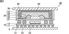
- the heat radiating structure 1B shown in FIG. 5 has the same configuration as the heat radiating structure 1 shown in FIG. 1 except that the heat conductive material layer 60 is arranged between the sealing material 23 and the heat radiating member 30. Is.
- the heat conductive material layer 60 is arranged between the sealing material 23 and the heat radiating member 30, the heat passing through the sealing material 23 easily reaches the heat radiating member 30. As a result, the heat dissipation efficiency is further improved.
- the heat conductive material layer 60 is also called a heat interface material (Thermal Interface Materials: TIM), and is preferably made of a heat conductive resin material such as a resin mixed with a heat conductive filler.
- TIM Thermal Interface Materials
- the heat conductive material layer 60 has an effect of bringing the second package 20 and the heat radiating member 30 into close contact with each other, and it is possible to prevent the heat radiating member 30 from shifting.
- FIG. 6 is a cross-sectional view schematically showing another modified example of the heat radiating structure according to the first embodiment of the present invention.
- the heat radiating structure 1C shown in FIG. 6 has the heat radiating structure 1 shown in FIG. 1 except that the heat transfer member 40 has a first portion 40a in contact with the sealing material 23 and an exposed second portion 40b. It has the same configuration as.
- the range of the first portion 40a in contact with the sealing material 23 and the range of the exposed second portion 40b are not particularly limited.
- the heat transfer member 40 may be the exposed second portion 40b.
- the heat transfer member 40 may be embedded in the sealing material 23 so that the second portion 40b is exposed. Even with such a configuration, the heat generated from the first electronic element 12 and the second electronic element 22 can be transferred to the heat radiating member 30 via the heat transfer member 40. Further, heat can be dissipated to the outside from the exposed second portion 40b of the heat transfer member 40. Therefore, the heat dissipation efficiency is improved.
- the heat transfer member 40 may have a third portion that comes into contact with something other than the sealing material 23.
- the heat transfer member and the sealing material are in contact with each other, but in the heat radiating structure according to the first embodiment of the present invention, heat transfer is performed.
- the member and the sealing material may not come into contact with each other, and a space may exist between them. Even with such a configuration, the heat generated from the first electronic element and the second electronic element can be transferred to the heat radiating member via the heat transfer member.
- the method for manufacturing a heat radiating structure according to the first embodiment of the present invention includes a second package manufacturing step, a package laminating step, and a heat radiating member arranging step.
- 7A and 7B are process diagrams schematically showing a second package manufacturing process in the method for manufacturing a heat radiating structure of the present invention.
- the second electronic element 22 and the heat transfer member 40 are arranged on the second substrate 21. It is preferable that the positions where the second electronic element 22 and the heat transfer member 40 are arranged are appropriately set according to the wiring 25 on the second substrate 21. At this time, the second electronic element 22 and the wiring 25 may be connected by wire bonding using the wire 24. As the wire bonding method, a usual method in the present technical field can be adopted. Further, the heat transfer member 40 may be connected to the wiring 25 by using solder.
- the sealing material 23 seals the second electronic element 22 and the heat transfer member 40 arranged on the second substrate 21. At this time, the upper end of the heat transfer member 40 is exposed from the sealing material 23. Examples of the method of exposing the upper end of the heat transfer member 40 from the sealing material 23 include a method of covering the heat transfer member 40 with the sealing material 23 and then exposing it by polishing.
- the second package 20 can be manufactured through the above steps.
- a first package in which the first electronic element is arranged on the first substrate is prepared.
- the second package manufactured in the second package manufacturing process is laminated on the first package.
- the first package and the second package may be joined by arranging solder between the first package and the second package and heating the solder. Further, if necessary, the first package and the second package may be adhered using a conductive adhesive or an insulating adhesive.
- Heat dissipation member placement process A heat radiating member is placed on the second package. At this time, the heat transfer member exposed from the sealing material and the heat radiating member are brought into contact with each other. Then, the second package and the heat radiating member are joined.
- the second package and the heat radiating member may be joined by joining the heat transfer member exposed from the sealing material and the heat radiating member with solder. .. In this case, the solder that comes into contact with the heat radiating member becomes a part of the heat transfer member in the heat radiating structure of the present invention. Further, the second package and the heat radiating member may be joined by welding. This step may be performed before laminating the second package on the first package.
- the heat radiating structure according to the first embodiment of the present invention can be obtained. Can be manufactured.
- the first package may be arranged on the main board, and then the second package and the heat radiating member may be arranged.
- the main board, the first board, and the second board are not particularly limited, but ordinary wiring boards used in the present technical field can be used.
- the first electronic element is not particularly limited, but a processor, a power source, or the like is preferable.
- the processor is not particularly limited, and may be, for example, a CPU (Central Processing Unit), a GPU (Graphics Processing Unit), an APU (Accelerated Processing Unit), or the like.
- the first electronic element is an APU
- the amount of heat generated during the operation of the APU is large, but the heat dissipation structure of the present invention can sufficiently dissipate the heat generated from the AUP. Therefore, the function of the APU is less likely to deteriorate.
- the first electronic element 12 is exposed, but in the heat radiating structure according to the first embodiment of the present invention, even if the first electronic element is sealed with a sealing material. good.
- the second electronic element is not particularly limited, but is preferably a semiconductor memory, a processor, a power supply, or the like. Further, when the heat radiating structure according to the first embodiment of the present invention is the heat radiating structure 1A shown in FIG. 4, the second electronic element may be an electronic element that generates noise, and is a semiconductor memory. It is preferable to have.
- the second electronic element 22 is electrically connected to the wiring 25 formed on the second substrate 21 by the wire 24, but the first embodiment of the present invention.
- the connection method is not particularly limited as long as the second electronic element can function.
- the connection terminal of the second electronic element may be arranged on the second substrate side, and the second electronic element and the wiring may be connected by solder.
- the material of the sealing material is not particularly limited, but a resin such as an epoxy resin is preferable.
- the thermal conductivity of the encapsulant is usually 0.1 W / m ⁇ K or more and 5 W / m ⁇ K or less.
- the “thermal conductivity of the encapsulant” means a value measured by a laser flash method based on JIS R1611: 2010.
- the material of the heat transfer member is not particularly limited, but is preferably metal, and more preferably copper, copper alloy, aluminum or the like. Further, since these metals have conductivity, they are also preferable as a material for the heat transfer member of the heat dissipation structure 1A shown in FIG. Further, the heat transfer member may be composed of a plurality of materials. That is, a part of the heat transfer member may be made of a material different from the other parts. In this case, the thermal conductivity of the entire heat transfer member may be higher than the thermal conductivity of the encapsulant.
- the thermal conductivity of the heat transfer member is not particularly limited as long as it is higher than the thermal conductivity of the encapsulant, but is preferably 50 W / m ⁇ K or more, 400 W / m ⁇ K or less, and 200 W / m ⁇ K or more. , 400 W / m ⁇ K or less is more preferable.
- the “thermal conductivity of the heat transfer member” means a value measured by a laser flash method based on JIS R1611: 2010.
- the thermal conductivity of the heat transfer member and the thermal conductivity of the encapsulant are within the above ranges, the heat generated from the first electronic element and the second electronic element can be efficiently conducted to the heat radiating member. ..
- FIG. 8A is a side sectional view schematically showing an example of arrangement of heat transfer members in the heat radiation structure according to the first embodiment of the present invention.
- FIG. 8B is a plan sectional view taken along the line AA of FIG. 8A.
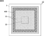
- the heat transfer member 40B has a continuous wall-like structure, and when the heat radiating structure 1D is viewed in a plan view in the stacking direction, the periphery of the second electronic element 22 is seen.
- the heat transfer member 40B may be arranged so as to surround the heat transfer member 40B.
- the thickness of the heat transfer member 40B is not constant in the stacking direction, and there may be a thin portion in a part or a thick portion in a part.
- FIG. 9A is a side sectional view schematically showing another example of arrangement of heat transfer members in the heat radiation structure according to the first embodiment of the present invention.
- 9B is a plan sectional view taken along the line BB of FIG. 9A.
- the heat transfer member 40C has a plurality of columnar structures, and surrounds the periphery of the second electronic element 22 when the heat radiating structure 1E is viewed in a plan view in the stacking direction.
- the heat transfer members 40C may be scattered and arranged as described above.
- the shape of the heat transfer member is not particularly limited as long as it is columnar, for example, a triangular columnar shape or the like. It may be polygonal columnar, columnar or elliptical columnar. Further, heat transfer members having two or more types of shapes may be arranged.
- the area of the cross section of the heat transfer member 40C perpendicular to the stacking direction is not constant in the stacking direction, and there may be a large portion in a part or a small portion in a part.
- the heat transfer member 40B and the heat transfer member 40C shown in FIGS. 8B and 9B surround the second electronic element 22 in a quadrangular shape.
- the shape surrounding the electronic element is not particularly limited, and may be enclosed in a triangular shape or may be enclosed in a circular shape. Further, it may be enclosed in a distorted shape according to the wiring of the second substrate, the shape of the second electronic element, and the like.
- the heat transfer member may have an upper plate.
- FIG. 10A is a side sectional view schematically showing an example of a case where the heat transfer member has an upper plate in the heat radiating structure according to the first embodiment of the present invention.
- FIG. 10B is a plan sectional view taken along the line CC of FIG. 10A.
- the heat radiating structure 1F shown in FIGS. 10A and 10B has the same structure as the heat radiating structure shown in FIGS. 8A and 8B except that the heat transfer member 40D has the upper plate 41. That is, in the heat radiating structure 1F shown in FIGS.
- the heat transfer member 40D further has an upper plate 41, the upper surface of the upper plate 41 is in contact with the heat radiating member 30, and the lower surface of the upper plate 41 is. It is joined to the upper end of the wall-shaped structure of the heat transfer member 40. With such a structure, heat can be transferred from the entire surface of the upper plate 41 to the heat radiating member 30, so that the heat radiating efficiency is further improved.
- the thickness of the upper plate 41 is not constant in the stacking direction, and there may be a thin portion in a part or a thick portion in a part.
- the heat radiating structure 1F shown in FIGS. 10A and 10B has the same structure as the heat radiating structure shown in FIGS. 8A and 8B except that the heat transfer member 40D has the upper plate 41.
- the body may have the same structure as the heat radiating structure shown in FIGS. 9A and 9B, except that the heat transfer member 40 has the upper plate 41. That is, the upper surface of the upper plate 41 may be in contact with the heat radiating member 30, and the lower surface of the upper plate 41 may be joined to the upper end of the columnar structure of the heat transfer member 40.
- the heat radiating member may be, for example, a heat sink or a heat pipe, but a vapor chamber is preferable.
- a vapor chamber is preferable.
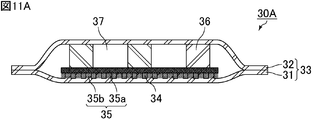
- FIG. 11A is a cross-sectional view schematically showing an example of a vapor chamber used in the heat radiating structure according to the first embodiment of the present invention.
- FIG. 11B is an enlarged cross-sectional view of a part of the vapor chamber shown in FIG. 11A.
- the vapor chamber 30A shown in FIG. 11A is formed on a housing 33 composed of a first sheet 31 and a second sheet 32 facing each other, a hydraulic fluid 34 sealed in the housing 33, and an inner wall surface of the first sheet 31. It has an arranged wick 35.
- the first sheet 31 and the second sheet 32 are joined to each other at the outer edge and sealed. Further, it is preferable that a plurality of columns 36 are arranged between the first sheet 31 and the second sheet 32 so as to support the first sheet 31 and the second sheet 32 from the inside.
- a steam flow path 37 composed of a cavity is provided inside the housing 33.
- the vapor flow path 37 is a flow path for moving the hydraulic fluid 34 of the gas phase, and communicates with the inside of the surface of the housing 33.
- the cavity between the inner wall surface of the second sheet 32 and the wick 35 constitutes the steam flow path 37.
- the first sheet 31 and the second sheet 32 are supported by the columns 36.
- the wick 35 includes a first wick 35a in contact with the steam flow path 37 and a second wick 35b arranged between the first wick 35a and the first sheet 31.
- the second wick 35b is provided on substantially the entire inner wall surface of the first sheet 31, and the first wick 35a is provided in contact with the surface of the second wick 35b.
- the first wick 35a is provided with a first liquid flow path 38a that penetrates in the thickness direction, which is the direction in which the first sheet 31 and the second sheet 32 face each other.
- the first liquid flow path 38a is a flow path for moving the hydraulic fluid 34 in the liquid phase in the thickness direction.
- the thickness direction is the vertical direction.
- the second wick 35b is provided with a second liquid flow path 38b that penetrates in the plane direction, which is a direction orthogonal to the thickness direction.
- the second liquid flow path 38b is a flow path for the hydraulic fluid 34 of the liquid phase to move in the plane direction.
- the surface direction is a direction parallel to the inner wall surface of the first sheet 31 and the second sheet 32.
- the average diameter of the first liquid flow path 38a seen from the thickness direction is preferably smaller than the average diameter of the second liquid flow path 38b seen from the direction through which the second liquid flow path 38b penetrates.
- the wick arranged on the inner wall surface of the first sheet 31 may include only the first wick 35a and the second wick 35b, between the first wick 35a and the second wick 35b, or with the second wick 35b.
- a third wick may be included between the first sheet 31 and a third wick between the first wick 35a and the second wick 35b, and between the second wick 35b and the first sheet 31.
- the wick 35 arranged on the inner wall surface of the first sheet 31 does not necessarily have to be arranged over the entire inner wall surface of the first sheet 31, and may be partially arranged.
- the wick 35 such as the first wick 35a and the second wick 35b is not particularly limited as long as it has a capillary structure capable of moving the hydraulic fluid by capillary force.
- the capillary structure of the wick 35 may be a known structure used in a conventional vapor chamber.
- Examples of the capillary structure include microstructures having irregularities such as pores, grooves, and protrusions, such as a porous structure, a fiber structure, a groove structure, and a mesh structure. These capillary structures form liquid flow paths such as the first liquid flow path 38a and the second liquid flow path 38b.
- the material of the wick 35 such as the first wick 35a and the second wick 35b is not particularly limited, and for example, a metal porous film, mesh, non-woven fabric, sintered body, porous body or the like formed by etching or metal processing is used. ..
- the mesh used as the material of the wick may be composed of, for example, a metal mesh, a resin mesh, or a surface-coated mesh thereof, and is preferably composed of a copper mesh, a stainless (SUS) mesh, or a polyester mesh.
- the sintered body used as the material of the wick may be composed of, for example, a metal porous sintered body and a ceramic porous sintered body, and is preferably composed of a copper or nickel porous sintered body. ..
- the porous body used as the material of the wick may be, for example, a porous body composed of a metal porous body, a ceramic porous body, a resin porous body, or the like.
- the first wick 35a is preferably composed of a mesh or a porous body
- the second wick 35b is preferably composed of a plurality of convex portions or concave portions provided on the inner wall surface of the first sheet 31.
- the convex portion or the concave portion may be formed directly on the inner wall surface of the first sheet 31, or may be provided by placing a metal foil having the convex portion or the concave portion on the inner wall surface of the first sheet 31. ..
- the first liquid flow path 38a is composed of through holes penetrating the first wick 35a in the thickness direction.
- the "diameter of the first liquid flow path 38a seen from the thickness direction” means “the minor diameter of the through hole seen from the thickness direction", and “the first liquid flow path seen from the thickness direction”.
- the “average diameter of 38a” means “the average value of the minor diameters of the through holes seen from the thickness direction”.
- the shape of the through hole when viewed from the thickness direction is not particularly limited, and the length of the portion closest to the diagonal is defined as the "minor diameter of the through hole".
- the wick 35 is arranged only on the inner wall surface of the first sheet 31, but the wick may be arranged on the inner wall surface of the second sheet.
- FIG. 12 is a cross-sectional view schematically showing an example of a heat radiating structure according to a second embodiment of the present invention.
- the heat radiating structure 101 shown in FIG. 12 includes a main board 2, a package 120 arranged on the main board 2, and a heat radiating member 30 arranged on the package 120.
- the package 120 includes a substrate 121, an electronic element 122 arranged on the substrate 121, and a sealing material 123 for sealing the electronic element 122.
- the electronic element 122 is electrically connected to the wiring 125 formed on the substrate 121 by, for example, a wire 124. Further, the main board 2 and the board 121 are connected by a solder ball 51.
- the heat radiating structure 101 includes a heat transfer member 40 arranged inside the sealing material 123 so as to penetrate the sealing material 123 in the stacking direction.
- the thermal conductivity of the heat transfer member 40 is higher than the thermal conductivity of the sealing material 123.
- the lower end of the heat transfer member 40 is in contact with the substrate 121, and the upper end of the heat transfer member 40 is in contact with the heat dissipation member 30.
- the electronic element 122 is not particularly limited, but is preferably a processor, a power source, a semiconductor memory, or the like. Among these, a processor having a large amount of heat generation is more preferable.
- the heat radiating structure according to the second embodiment can efficiently radiate heat generated from the electronic element 122 by the same principle as the heat radiating structure according to the first embodiment.
- FIG. 13 is a cross-sectional view schematically showing another modified example of the heat radiating structure according to the second embodiment of the present invention.
- the heat radiating structure 101A shown in FIG. 13 has a heat radiating structure 101 shown in FIG. 12, except that the heat transfer member 40 has a first portion 40a in contact with the sealing material 123 and an exposed second portion 40a. It has the same configuration as.
- the range of the first portion 40a in contact with the sealing material 123 and the range of the exposed second portion 40b are not particularly limited.
- the heat transfer member 40 may be the exposed second portion 40b.
- the heat transfer member 40 may be embedded in the sealing material 123 so that the second portion 40b is exposed. Even with such a configuration, the heat generated from the electronic element 122 can be transferred to the heat radiating member 30 via the heat transfer member 40. Further, heat can be dissipated to the outside from the exposed part 40b of the heat transfer member 40. Therefore, the heat dissipation efficiency is improved.
- the heat transfer member 40 may have a third portion that comes into contact with something other than the sealing material 123.
- the heat transfer member and the sealing material are in contact with each other, but in the heat radiating structure according to the second embodiment of the present invention, the heat transfer member is in contact with each other.
- the member and the sealing material may not come into contact with each other, and a space may exist between them. Even with such a configuration, the heat generated from the electronic element can be transferred to the heat radiating member via the heat transfer member.
- the heat dissipation structure of the present invention can be mounted on an electronic device for the purpose of heat dissipation. Therefore, the electronic device provided with the heat radiating member of the present invention is also one of the present inventions. Examples of the electronic device of the present invention include smartphones, tablet terminals, notebook computers, game devices, wearable devices, and the like.
- Heat transfer structure 2 Main board 10 1st package 11 1st substrate 12 1st electronic element 20 2nd package 21 2nd substrate 22 2nd electronic element 23 , 123 Encapsulant 24, 124 Wire 25, 125 Wiring 30 Heat transfer member 30A Vapor chamber 31 First sheet 32 Second sheet 33 Housing 34 Working fluid 35 Wick 35a First wick 35b Second wick 36 Strut 37 Steam flow path 38a 1st liquid flow path 38b 2nd liquid flow path 40, 40A, 40B, 40C, 40D Heat transfer member 40a 1st part 40b 2nd part 41 Top plate 51, 52, 53 Solder ball 60 Thermal conductive material layer 120 Package 121 Board 122 Electronic element
Landscapes
- Engineering & Computer Science (AREA)
- Microelectronics & Electronic Packaging (AREA)
- Power Engineering (AREA)
- Physics & Mathematics (AREA)
- Condensed Matter Physics & Semiconductors (AREA)
- General Physics & Mathematics (AREA)
- Computer Hardware Design (AREA)
- Thermal Sciences (AREA)
- Cooling Or The Like Of Semiconductors Or Solid State Devices (AREA)
Abstract
第1基板(11)、及び、上記第1基板(11)の上に配置された第1電子素子(12)を備える第1パッケージ(10)と、第2基板(21)、上記第2基板(21)の上に配置された第2電子素子(22)、及び、上記第2電子素子(22)を封止する封止材(23)を備え、上記第1パッケージ(10)の上に積層された第2パッケージ(20)と、上記第2パッケージ(20)の上に配置された放熱部材(30)と、上記第2基板(21)及び上記放熱部材(30)に接触する伝熱部材(40)とを備え、上記伝熱部材(40)の熱伝導率は、上記封止材(23)の熱伝導率よりも高いことを特徴とする放熱構造体(1)。
Description
本発明は、放熱構造体に関する。本発明はまた、上記放熱構造体を備える電子機器に関する。
CPU(Central Processing Unit)やGPU(Graphics Processing Unit)等の電子素子は、基板上に配置された後、樹脂等により封止(molding)されることで、半導体パッケージとして用いられる。電子素子は、動作時に高温となるため、電子素子の温度を下げなければ、電子素子の性能を発揮できなくなる場合がある。
近年、電子素子が高集積化、高性能化することにより、電子機器から発生する発熱量が増加している。また、製品の小型化が進むことで、発熱密度が増加するため、放熱対策が重要となってきた。この状況はスマートフォンやタブレットなどのモバイル端末の分野において特に顕著である。
このような、半導体パッケージから発生する熱を放熱するために、特許文献1には半導体パッケージの上に所定の放熱用部品を配置した半導体パッケージ放熱用部品が開示されている。
すなわち、特許文献1には、半導体パッケージ上に配置され、熱伝導部材に接する半導体パッケージ放熱用部品であって、当該放熱用部品の前記熱伝導部材と対向する面には、線状の高熱伝導性物質が熱伝導方向に林立するように形成され、前記線状の高熱伝導性物質の先端部は、前記熱伝導部材の表面に密着していることを特徴とする半導体パッケージ放熱用部品が開示されている。
特許文献1に記載の半導体パッケージ放熱用部品では、半導体パッケージの上に放熱用部材が配置されているので、半導体パッケージの表面に届いた熱を効率的に放熱することが可能であると考えられる。
すなわち、特許文献1には、半導体パッケージ上に配置され、熱伝導部材に接する半導体パッケージ放熱用部品であって、当該放熱用部品の前記熱伝導部材と対向する面には、線状の高熱伝導性物質が熱伝導方向に林立するように形成され、前記線状の高熱伝導性物質の先端部は、前記熱伝導部材の表面に密着していることを特徴とする半導体パッケージ放熱用部品が開示されている。
特許文献1に記載の半導体パッケージ放熱用部品では、半導体パッケージの上に放熱用部材が配置されているので、半導体パッケージの表面に届いた熱を効率的に放熱することが可能であると考えられる。
半導体パッケージにおける発熱源は、半導体パッケージ内部にある電子素子であり、電子素子から発生した熱が、半導体パッケージの表面にまで到達するには、樹脂等の封止材を通過する必要がある。
このような樹脂等の封止材は、通常、熱伝導率が低い材料から構成されるので、発熱源である電子素子から半導体パッケージの表面までの伝熱効率が低くなる。
特許文献1では、半導体パッケージ内の発熱源である電子素子から、半導体パッケージの表面までの伝熱については何ら考慮されていない。そのため、特許文献1に記載の半導体パッケージ放熱用部品では、電子素子から、半導体パッケージの表面までの伝熱については放熱効率が充分に高くないという問題があった。
このような樹脂等の封止材は、通常、熱伝導率が低い材料から構成されるので、発熱源である電子素子から半導体パッケージの表面までの伝熱効率が低くなる。
特許文献1では、半導体パッケージ内の発熱源である電子素子から、半導体パッケージの表面までの伝熱については何ら考慮されていない。そのため、特許文献1に記載の半導体パッケージ放熱用部品では、電子素子から、半導体パッケージの表面までの伝熱については放熱効率が充分に高くないという問題があった。
また、近年、電子素子の集積度を高めるため、パッケージに別のパッケージを積層するパッケージ・オン・パッケージ(package on package:PoP)構造がよく採用されている。
このようなPoP構造において下層に高熱源体となる電子素子を配置すると、下層で発生した熱は、上層の半導体パッケージにおける基板や樹脂層等の熱伝導率が低い領域を通って、外部に放熱されることになる。
そのため、このようなPoP構造では、より熱が籠りやすくなるという問題があった。
このようなPoP構造において下層に高熱源体となる電子素子を配置すると、下層で発生した熱は、上層の半導体パッケージにおける基板や樹脂層等の熱伝導率が低い領域を通って、外部に放熱されることになる。
そのため、このようなPoP構造では、より熱が籠りやすくなるという問題があった。
本発明は、上記問題を解決するためになされたものであり、本発明の目的は、電子素子から発生する熱を効率的に放熱することができる放熱構造体を提供することである。また、本発明の目的は、上記放熱構造体を備える電子機器を提供することである。
本発明の放熱構造体は、第1の態様において、第1基板、及び、上記第1基板の上に配置された第1電子素子を備える第1パッケージと、第2基板、上記第2基板の上に配置された第2電子素子、及び、上記第2電子素子を封止する封止材を備え、上記第1パッケージの上に積層された第2パッケージと、上記第2パッケージの上に配置された放熱部材と、上記第2基板及び上記放熱部材に接触する伝熱部材とを備え、上記伝熱部材の熱伝導率は、上記封止材の熱伝導率よりも高いことを特徴とする。
本発明の放熱構造体は、第2の態様において、基板、及び、上記基板の上に配置された電子素子、及び、上記電子素子を封止する封止材を備えるパッケージと、上記パッケージの上に配置された放熱部材と、上記基板及び上記放熱部材に接触する伝熱部材とを備え、上記伝熱部材の熱伝導率は、上記封止材の熱伝導率よりも高いことを特徴とする。
本発明の電子機器は、本発明の放熱構造体を備えることを特徴とする。
本発明によれば、電子素子から発生する熱を効率的に放熱することができる放熱構造体を提供することができる。
以下、本発明の放熱構造体について説明する。
しかしながら、本発明は、以下の構成に限定されるものではなく、本発明の要旨を変更しない範囲において適宜変更して適用することができる。なお、以下において記載する本発明の個々の望ましい構成を2つ以上組み合わせたものもまた本発明である。
しかしながら、本発明は、以下の構成に限定されるものではなく、本発明の要旨を変更しない範囲において適宜変更して適用することができる。なお、以下において記載する本発明の個々の望ましい構成を2つ以上組み合わせたものもまた本発明である。
以下に示す各実施形態は例示であり、異なる実施形態で示した構成の部分的な置換又は組み合わせが可能であることは言うまでもない。第2実施形態以降では、第1実施形態と共通の事項についての記述は省略し、異なる点についてのみ説明する。特に、同様の構成による同様の作用効果については、実施形態毎には逐次言及しない。
以下の説明において、各実施形態を特に区別しない場合、単に「本発明の放熱構造体」という。
[第1実施形態]
本発明の第1実施形態に係る放熱構造体について説明する。
図1は、本発明の第1実施形態に係る放熱構造体の一例を模式的に示す断面図である。
本発明の第1実施形態に係る放熱構造体について説明する。
図1は、本発明の第1実施形態に係る放熱構造体の一例を模式的に示す断面図である。
図1に示す放熱構造体1は、メインボード2と、メインボード2の上に配置された第1パッケージ10と、第1パッケージ10の上に積層された第2パッケージ20と、第2パッケージ20の上に配置された放熱部材30とを備える。
なお、本明細書において、便宜上、放熱構造体1における積層方向の第1パッケージ10に対する第2パッケージ20側を「上」と記載するが、「上」は、鉛直方向の上側を意味するものではなく、第1パッケージに対し、第2パッケージが積層される側の方向を意味する。
なお、本明細書において、便宜上、放熱構造体1における積層方向の第1パッケージ10に対する第2パッケージ20側を「上」と記載するが、「上」は、鉛直方向の上側を意味するものではなく、第1パッケージに対し、第2パッケージが積層される側の方向を意味する。
第1パッケージ10は、第1基板11、及び、第1基板11の上に配置された第1電子素子12を備える。
第1電子素子12は、例えば、半田ボール52により第1基板11の上に形成された配線(図示せず)と電気的に接続されている。
第1電子素子12は、例えば、半田ボール52により第1基板11の上に形成された配線(図示せず)と電気的に接続されている。
第2パッケージ20は、第2基板21、第2基板21の上に配置された第2電子素子22、及び、第2電子素子22を封止する封止材23を備える。
第2電子素子22は、例えば、ワイヤ24により、第2基板21の上に形成された配線25と電気的に接続されている。
第2電子素子22は、例えば、ワイヤ24により、第2基板21の上に形成された配線25と電気的に接続されている。
放熱構造体1は、封止材23を積層方向に貫通するように封止材23の内部に配置された伝熱部材40を備えている。
伝熱部材40の熱伝導率は、封止材23の熱伝導率よりも高い。
伝熱部材40の下端は、第2基板21と接触しており、伝熱部材40の上端は、放熱部材30と接触している。
伝熱部材40の熱伝導率は、封止材23の熱伝導率よりも高い。
伝熱部材40の下端は、第2基板21と接触しており、伝熱部材40の上端は、放熱部材30と接触している。
なお、本発明の放熱構造体では、伝熱部材が、第2基板及び放熱部材と接触していればどのような態様であってもよい。例えば、伝熱部材の一方の端部が第2基板に接触し、伝熱部材の他方の端部が放熱部材に接触していてもよい。また、伝熱部材が第2基板を貫通し、伝熱部材と第2基板の貫通孔の側壁とが接触していてもよく、伝熱部材が放熱部材を貫通し、伝熱部材と放熱部材の貫通孔の側壁とが接触していてもよい。
メインボード2と第1パッケージ10の第1基板11とは半田ボール51により接続されている。また、第1パッケージ10の第1基板11と、第2パッケージ20の第2基板21とは、半田ボール53により接続されている。
図1に示す放熱構造体1は、いわゆるパッケージ・オン・パッケージ(PoP)構造である。
ここで、放熱構造体において伝熱部材が配置されていない場合の熱の流れについて説明する。
図2は、伝熱部材が配置されていない従来の放熱構造体における熱の流れを模式的に示す模式図である。
図2に示す放熱構造体1´は、伝熱部材が配置されていない以外、上記放熱構造体1と同じ構造である。
放熱構造体1´において、第1電子素子12及び第2電子素子22が作動する場合、これらから熱が発生する。
図2に示す放熱構造体1´において、第1電子素子12から発生した熱は、半田ボール52、第1基板11上の配線(図示せず)、半田ボール53、第2基板21及び封止材23を介して放熱部材30に到達する。なお、図2において、第1電子素子12から発生する熱の流れの方向を矢印Hで示す。しかし、通常、封止材の熱伝導率は高くないので、熱は放熱部材30に到達しにくい。
その結果、熱は、放熱構造体1´に籠りやすくなる。
なお、第2電子素子22から熱が発生する場合も、熱は、封止材23を介して放熱部材30に到達するので、熱は放熱部材30に到達しにくい。
次に、放熱構造体1の熱の流れについて説明する。
図3は、図1に示す放熱構造体における熱の流れを模式的に示す模式図である。
放熱構造体1において、第1電子素子12及び第2電子素子22が作動する場合、これらから熱が発生する。
図3に示すように、第1電子素子12から発生した熱は、半田ボール52、第1基板11の配線(図示せず)、半田ボール53及び第2基板21に到達する。なお、図3において第1電子素子12から発生する熱の流れの方向を矢印Hで示す。ここで、一部の熱は、封止材23を通り放熱部材30まで到達するが、大部分の熱は、伝熱部材40の内部を通り、放熱部材30まで到達する。
第2電子素子22から熱が発生する場合も、一部の熱は封止材23を介して放熱部材30に到達するが、大部分の熱は、第2基板21の配線、及び、伝熱部材40の内部を通り、放熱部材30まで到達する。
特に、第2パッケージ20において、第2電子素子22は、第2基板21との距離が近く、第2電子素子22から発生した熱は、第2基板21の配線に伝熱されやすい。
放熱構造体1では、伝熱部材40の熱伝導率が、封止材23の熱伝導率よりも高いので、熱の大部分は、伝熱部材40を通って速やかに、放熱部材30まで到達する。そのため、放熱構造体1では、発生した熱を速やかに放熱することができるので、放熱構造体1´のように熱が籠ることを防止することができる。すなわち、電子素子から発生する熱を効率的に放熱することができる。
第1基板及び第2基板に配置される配線の材料としては、銅、銀、アルミニウム等であることが好ましい。これらの材料は、熱伝導率が高いので、配線がこれらの材料からなると、第1電子素子及び第2電子素子から発生した熱が伝熱されやすくなる。
次に、本発明の第1実施形態に係る放熱構造体の変形例について説明する。
図4は、本発明の第1実施形態に係る放熱構造体の変形例の一例を模式的に示す断面図である。
図4に示す放熱構造体1Aは、放熱部材30の筐体及び伝熱部材40Aが導電性を有し、放熱部材30と、配線25とが、伝熱部材40Aを介して電気的に接続されており、放熱部材30が外部グランドと電気的に接続されていること以外は、図1に示す放熱構造体1と同じ構成である。
図4は、本発明の第1実施形態に係る放熱構造体の変形例の一例を模式的に示す断面図である。
図4に示す放熱構造体1Aは、放熱部材30の筐体及び伝熱部材40Aが導電性を有し、放熱部材30と、配線25とが、伝熱部材40Aを介して電気的に接続されており、放熱部材30が外部グランドと電気的に接続されていること以外は、図1に示す放熱構造体1と同じ構成である。
図4に示す放熱構造体1Aにおいて、第2電子素子22においてノイズ電流が発生した場合、配線25、伝熱部材40A及び放熱部材30の順に、ノイズ電流を流すことができる。なお、図4においてノイズ電流の流れを矢印Nで示す。さらに、外部グランドとして機能する電子機器の筐体と放熱部材30とを接触させることにより、このようなノイズ電流を外部グランドに流すことができる。
このように、伝熱部材40Aを介して、ノイズ電流を外部グランドに流すことにより、ノイズ電流が流れる距離を短くすることができ、ノイズ電流に起因する誤作動を防止することができる。
このように、伝熱部材40Aを介して、ノイズ電流を外部グランドに流すことにより、ノイズ電流が流れる距離を短くすることができ、ノイズ電流に起因する誤作動を防止することができる。
図4に示す放熱構造体1Aにおいて、第2電子素子22は、半導体メモリであることが好ましい。また、半導体メモリは積層されていてもよい。
半導体メモリとしては、DRAM(Random Access Memory)回路等が挙げられる。半導体メモリは、ダイアタッチメントフィルム等を介して積層されていることが好ましい。
図4に示す放熱構造体1Aにおいて、第2電子素子22がDRAM回路である場合、DRAM回路のグランドは、第2基板21、半田ボール53、第1基板11及び半田ボール51を介して、メインボード2のグランドに接続されることになる。そのため、DRAM回路のグランドインピーダンスは配線抵抗及び配線インダクタンスが高くなりDRAMの同時スイッチングによりノイズを発生させることになる。しかし、伝熱部材40Aがグランド配線とで接触していることにより、DRAM回路と放熱部材30とが電気的に接続されるので、グランドインピーダンスを低減し、スイッチングノイズを抑制できる。
図4に示す放熱構造体1Aでは、配線25がグランド配線を含み、伝熱部材40Aの一部はグランド配線と接触していることが好ましい。
第2電子素子22から発生した熱は、配線25を流れることになる。配線25がグランド配線を含んでいる場合、グランド配線は最も配線が多いので、グランド配線を通る熱の量も多くなる。伝熱部材40Aがグランド配線と接触していると、グランド配線を通る熱を、速やかに放熱部材30に伝熱することができる。その結果、放熱効率が向上する。
第2電子素子22から発生した熱は、配線25を流れることになる。配線25がグランド配線を含んでいる場合、グランド配線は最も配線が多いので、グランド配線を通る熱の量も多くなる。伝熱部材40Aがグランド配線と接触していると、グランド配線を通る熱を、速やかに放熱部材30に伝熱することができる。その結果、放熱効率が向上する。
次に、本発明の第1実施形態に係る放熱構造体の別の変形例について説明する。
図5は、本発明の第1実施形態に係る放熱構造体の別の変形例の一例を模式的に示す断面図である。
図5に示す放熱構造体1Bは、封止材23と、放熱部材30との間に、熱伝導性材料層60が配置されていること以外は、図1に示す放熱構造体1と同じ構成である。
図5は、本発明の第1実施形態に係る放熱構造体の別の変形例の一例を模式的に示す断面図である。
図5に示す放熱構造体1Bは、封止材23と、放熱部材30との間に、熱伝導性材料層60が配置されていること以外は、図1に示す放熱構造体1と同じ構成である。
上述した通り、第1電子素子12及び第2電子素子22から発生する熱の一部は、封止材23を通って放熱部材30に到達する。
封止材23と放熱部材30との間に、熱伝導性材料層60が配置されている場合、封止材23を通る熱が、放熱部材30に到達しやすくなる。その結果、放熱効率がさらに向上する。
封止材23と放熱部材30との間に、熱伝導性材料層60が配置されている場合、封止材23を通る熱が、放熱部材30に到達しやすくなる。その結果、放熱効率がさらに向上する。
なお、熱伝導性材料層60とは、熱界面材料(Thermal Interface Materials:TIM)とも呼ばれ、例えば、熱伝導フィラーを混合した樹脂等の熱伝導性樹脂材料からなることが好ましい。
また、熱伝導性材料層60には、第2パッケージ20と、放熱部材30とを密着させる効果があり、放熱部材30がずれることを防止することができる。
次に、本発明の第1実施形態に係る放熱構造体の別の変形例について説明する。
図6は、本発明の第1実施形態に係る放熱構造体の別の変形例の一例を模式的に示す断面図である。
図6に示す放熱構造体1Cは、伝熱部材40が、封止材23に接触する第1部分40aと、露出する第2部分40bとを有すること以外は、図1に示す放熱構造体1と同じ構成である。
なお、放熱構造体1Cでは、封止材23に接触する第1部分40aの範囲、及び、露出する第2部分40bの範囲は特に限定されない。
例えば、放熱構造体1Cでは、第1部分40aがわずかでも封止材23に接触していれば、伝熱部材40の大部分が、露出する第2部分40bであってもよい。
また、放熱構造体1Cでは、伝熱部材40の第2部分40bがわずかでも露出していれば、伝熱部材40の大部分が、封止材23に接触する第1部分40aであってもよい。
さらに、伝熱部材40は、第2部分40bが露出するように封止材23に埋まっていてもよい。
このような構成であっても、第1電子素子12及び第2電子素子22から発生した熱を、伝熱部材40を介して放熱部材30に伝熱することができる。
さらに、伝熱部材40の露出第2部分40bから熱を外部に放熱することができる。そのため放熱効率が向上する。
なお、伝熱部材40は、封止材23以外のものと接触する第3部分を有していてもよい。
これまで説明してきた本発明の第1実施形態に係る放熱構造体では、伝熱部材と封止材とは接触していたが、本発明の第1実施形態に係る放熱構造体では、伝熱部材と封止材とは接触せず、これらの間に空間が存在していてもよい。
このような構成であっても、第1電子素子及び第2電子素子から発生した熱を、伝熱部材を介して放熱部材に伝熱することができる。
このような構成であっても、第1電子素子及び第2電子素子から発生した熱を、伝熱部材を介して放熱部材に伝熱することができる。
次に、本発明の第1実施形態に係る放熱構造体の製造方法の一例について説明する。
本発明の第1実施形態に係る放熱構造体の製造方法は、第2パッケージ製造工程、パッケージ積層工程及び放熱部材配置工程を含む。
本発明の第1実施形態に係る放熱構造体の製造方法は、第2パッケージ製造工程、パッケージ積層工程及び放熱部材配置工程を含む。
(第2パッケージ製造工程)
以下に図面を用いて、第2パッケージ製造工程について説明する。
図7A及び図7Bは、本発明の放熱構造体の製造方法における第2パッケージ製造工程を模式的に示す工程図である。
以下に図面を用いて、第2パッケージ製造工程について説明する。
図7A及び図7Bは、本発明の放熱構造体の製造方法における第2パッケージ製造工程を模式的に示す工程図である。
まず、図7Aに示すように、第2基板21の上に第2電子素子22及び伝熱部材40を配置する。
第2電子素子22及び伝熱部材40を配置する位置は、第2基板21上の配線25に合わせ適宜設定することが好ましい。
なお、この際、第2電子素子22と配線25とを、ワイヤ24を用いてワイヤボンディングにより接続してもよい。ワイヤボンディングの方法としては、本技術分野における通常の方法を採用することができる。
また、半田を用いて、伝熱部材40を配線25に接続してもよい。
第2電子素子22及び伝熱部材40を配置する位置は、第2基板21上の配線25に合わせ適宜設定することが好ましい。
なお、この際、第2電子素子22と配線25とを、ワイヤ24を用いてワイヤボンディングにより接続してもよい。ワイヤボンディングの方法としては、本技術分野における通常の方法を採用することができる。
また、半田を用いて、伝熱部材40を配線25に接続してもよい。
次に、図7Bに示すように、封止材23により、第2基板21の上に配置された第2電子素子22及び伝熱部材40を封止する。
この際、伝熱部材40の上端が封止材23から露出するようにする。
伝熱部材40の上端を封止材23から露出させる方法としては、例えば、一旦、伝熱部材40を封止材23で覆ってから研磨により露出させる方法が挙げられる。
この際、伝熱部材40の上端が封止材23から露出するようにする。
伝熱部材40の上端を封止材23から露出させる方法としては、例えば、一旦、伝熱部材40を封止材23で覆ってから研磨により露出させる方法が挙げられる。
以上の工程を経て第2パッケージ20を作製することができる。
(パッケージ積層工程)
別途、第1基板の上に第1電子素子が配置された第1パッケージを準備する。
そして、第1パッケージの上に上記第2パッケージ製造工程で製造した第2パッケージを積層する。
この際、第1パッケージ及び第2パッケージとの間に半田を配置し、加熱することにより第1パッケージ及び第2パッケージを接合してもよい。
また、必要に応じて、導電性接着材や絶縁性接着材を用いて第1パッケージ及び第2パッケージを接着してもよい。
別途、第1基板の上に第1電子素子が配置された第1パッケージを準備する。
そして、第1パッケージの上に上記第2パッケージ製造工程で製造した第2パッケージを積層する。
この際、第1パッケージ及び第2パッケージとの間に半田を配置し、加熱することにより第1パッケージ及び第2パッケージを接合してもよい。
また、必要に応じて、導電性接着材や絶縁性接着材を用いて第1パッケージ及び第2パッケージを接着してもよい。
(放熱部材配置工程)
第2パッケージの上に、放熱部材を配置する。この際、封止材から露出する伝熱部材と、放熱部材とが接触するようにする。そして、第2パッケージ及び放熱部材を接合する。
第2パッケージ及び放熱部材を接合する方法としては、例えば、封止材から露出する伝熱部材と、放熱部材とを半田で接合することにより、第2パッケージと放熱部材とを接合してもよい。この場合、放熱部材と接触する半田は、本発明の放熱構造体における伝熱部材の一部となる。また、第2パッケージ及び放熱部材を溶接により接合してもよい。
なお、この工程は、第1パッケージに第2パッケージを積層する前に行ってもよい。
第2パッケージの上に、放熱部材を配置する。この際、封止材から露出する伝熱部材と、放熱部材とが接触するようにする。そして、第2パッケージ及び放熱部材を接合する。
第2パッケージ及び放熱部材を接合する方法としては、例えば、封止材から露出する伝熱部材と、放熱部材とを半田で接合することにより、第2パッケージと放熱部材とを接合してもよい。この場合、放熱部材と接触する半田は、本発明の放熱構造体における伝熱部材の一部となる。また、第2パッケージ及び放熱部材を溶接により接合してもよい。
なお、この工程は、第1パッケージに第2パッケージを積層する前に行ってもよい。
次に、メインボードの上に第1パッケージが配置されるように、第1パッケージ、第2パッケージ及び放熱部材の積層体を配置することにより、本発明の第1実施形態に係る放熱構造体を製造することができる。
なお、本発明の第1実施形態に係る放熱構造体の製造方法では、第1パッケージをメインボードに配置してから、第2パッケージ及び放熱部材を配置してもよい。
なお、本発明の第1実施形態に係る放熱構造体の製造方法では、第1パッケージをメインボードに配置してから、第2パッケージ及び放熱部材を配置してもよい。
本発明の第1実施形態に係る放熱構造体の各構成の好ましい態様を以下に説明する。
本発明の第1実施形態に係る放熱構造体において、メインボード、第1基板及び第2基板としては、特に限定されないが、本技術分野で使用される通常の配線基板を用いることができる。
本発明の第1実施形態に係る放熱構造体において、第1電子素子としては、特に限定されないが、プロセッサ、電源等であることが好ましい。
また、プロセッサとしては、特に限定されず、例えばCPU(Central Processing Unit)、GPU(Graphics Processing Unit)、APU(Accelerated Processing Unit)等であってもよい。
特に、第1電子素子がAPUである場合、APUの作動時の発熱量が多いが、本発明の放熱構造体は、AUPから発生する熱を充分に放熱することができる。そのため、APUの機能が低下しにくくなる。
また、プロセッサとしては、特に限定されず、例えばCPU(Central Processing Unit)、GPU(Graphics Processing Unit)、APU(Accelerated Processing Unit)等であってもよい。
特に、第1電子素子がAPUである場合、APUの作動時の発熱量が多いが、本発明の放熱構造体は、AUPから発生する熱を充分に放熱することができる。そのため、APUの機能が低下しにくくなる。
図1に示す放熱構造体1では、第1電子素子12はむき出しであるが、本発明の第1実施形態に係る放熱構造体では、第1電子素子は封止材で封止されていてもよい。
第2電子素子としては、特に限定されないが、半導体メモリ、プロセッサ、電源等であることが好ましい。
また、本発明の第1実施形態に係る放熱構造体が、図4に示す放熱構造体1Aである場合、第2電子素子としては、ノイズを発生する電子素子であってもよく、半導体メモリであることが好ましい。
また、本発明の第1実施形態に係る放熱構造体が、図4に示す放熱構造体1Aである場合、第2電子素子としては、ノイズを発生する電子素子であってもよく、半導体メモリであることが好ましい。
図1に示す放熱構造体1では、第2電子素子22は、ワイヤ24により、第2基板21の上に形成された配線25と電気的に接続されているが、本発明の第1実施形態に係る放熱構造体では、第2電子素子が機能することができればその接続方法は特に限定されない。例えば、第2電子素子の接続端子が第2基板側に配置されており、第2電子素子と、配線とが半田により接続されていてもよい。
本発明の第1実施形態に係る放熱構造体では、封止材の材料としては、特に限定されないが、エポキシ樹脂等の樹脂であることが好ましい。
封止材の熱伝導率は、通常、0.1W/m・K以上、5W/m・K以下である。
なお、本明細書において、「封止材の熱伝導率」とは、JIS R1611:2010に基づくレーザーフラッシュ法により測定された値を意味する。
なお、本明細書において、「封止材の熱伝導率」とは、JIS R1611:2010に基づくレーザーフラッシュ法により測定された値を意味する。
本発明の第1実施形態に係る放熱構造体では、伝熱部材の材料としては、特に限定されないが、金属であることが好ましく、銅、銅合金、アルミニウム等であることがより好ましい。さらに、これらの金属は、導電性を有するので、図4に示す放熱構造体1Aの伝熱部材の材料としても好ましい。
また、伝熱部材は、複数の材料から構成されていてもよい。つまり、伝熱部材の一部が、他の部分と異なる材料からなっていてもよい。この場合、伝熱部材全体の熱伝導率が、封止材の熱伝導率よりも高ければよい。
また、伝熱部材は、複数の材料から構成されていてもよい。つまり、伝熱部材の一部が、他の部分と異なる材料からなっていてもよい。この場合、伝熱部材全体の熱伝導率が、封止材の熱伝導率よりも高ければよい。
伝熱部材の熱伝導率は、封止材の熱伝導率よりも高ければ特に限定されないが、50W/m・K以上、400W/m・K以下であることが好ましく、200W/m・K以上、400W/m・K以下であることがより好ましい。
本明細書において、「伝熱部材の熱伝導率」とは、JIS R1611:2010に基づくレーザーフラッシュ法により測定された値を意味する。
本明細書において、「伝熱部材の熱伝導率」とは、JIS R1611:2010に基づくレーザーフラッシュ法により測定された値を意味する。
本発明の第1実施形態に係る放熱構造体では、伝熱部材の熱伝導率と、封止材の熱伝導率との比は、[伝熱部材の熱伝導率]/[封止材の熱伝導率]=10/1以上、3000/1以下であることが好ましい。
伝熱部材の熱伝導率、及び、封止材の熱伝導率が、上記範囲であると、第1電子素子及び第2電子素子から発生した熱を効率的に放熱部材まで伝導することができる。
次に、本発明の放熱構造体における伝熱部材の形状及び配置について説明する。
図8Aは、本発明の第1実施形態に係る放熱構造体における伝熱部材の配置の一例を模式的に示す側面断面図である。図8Bは、図8AのA-A線に沿った平面断面図である。
図8Aは、本発明の第1実施形態に係る放熱構造体における伝熱部材の配置の一例を模式的に示す側面断面図である。図8Bは、図8AのA-A線に沿った平面断面図である。
図8A及び図8Bに示すように、伝熱部材40Bは、連続した壁状の構造を有しており、放熱構造体1Dを積層方向に平面視した際に、第2電子素子22の周囲を囲むように伝熱部材40Bが配置されていてもよい。
伝熱部材40Bの厚さは、積層方向に一定でなく、一部に薄い部分があってもよく、一部に厚い部分があってもよい。
伝熱部材40Bの厚さは、積層方向に一定でなく、一部に薄い部分があってもよく、一部に厚い部分があってもよい。
図9Aは、本発明の第1実施形態に係る放熱構造体における伝熱部材の配置の別の一例を模式的に示す側面断面図である。図9Bは、図9AのB-B線に沿った平面断面図である。
図9A及び図9Bに示すように、伝熱部材40Cは、複数の柱状の構造を有しており、放熱構造体1Eを積層方向に平面視した際に、第2電子素子22の周囲を囲むように伝熱部材40Cが点在して配置されていてもよい。
なお、図9A及び図9Bに示す伝熱部材40Cは四角柱状であるが、本発明の放熱構造体では、伝熱部材は、柱状であればその形状は特に限定されず、例えば三角柱状等の多角柱状であってもよく、円柱状や楕円柱状であってもよい。また、2種類以上の形状の伝熱部材が配置されていてもよい。
伝熱部材40Cの積層方向に垂直な断面の面積は、積層方向に一定でなく、一部に大きい部分があってもよく、一部に小さい部分があってもよい。
図8B及び図9Bに示す伝熱部材40B及び伝熱部材40Cは、第2電子素子22の周囲を四角形状に囲っているが、本発明の第1実施形態に係る放熱構造体では、第2電子素子を囲う形状は特に限定されず、三角形状に囲っていてもよく、円形に囲っていてもよい。
さらに、第2基板の配線や、第2電子素子の形状等に合わせて、いびつな形状で囲っていてもよい。
さらに、第2基板の配線や、第2電子素子の形状等に合わせて、いびつな形状で囲っていてもよい。
さらに、本発明の放熱構造体では伝熱部材が上板を有していてもよい。伝熱部材が上板を有する場合について図面を用いて説明する。
図10Aは、本発明の第1実施形態に係る放熱構造体において、伝熱部材が上板を有する場合の一例を模式的に示す側面断面図である。図10Bは、図10AのC-C線に沿った平面断面図である。
図10A及び図10Bに示す放熱構造体1Fは、伝熱部材40Dが上板41を有する以外は、図8A及び図8Bに示す放熱構造体と同じ構造である。
すなわち、図10A及び図10Bに示す放熱構造体1Fでは、伝熱部材40Dは、さらに上板41を有し、上板41の上面は、放熱部材30と接触し、上板41の下面は、伝熱部材40の壁状の構造の上端と接合している。
このような構造であると、上板41の全面から、放熱部材30に熱が移動できるので、放熱効率がさらに向上する。
上板41の厚さは、積層方向に一定でなく、一部に薄い部分があってもよく、一部に厚い部分があってもよい。
なお、図10A及び図10Bに示す放熱構造体1Fでは、伝熱部材40Dが上板41を有する以外は、図8A及び図8Bに示す放熱構造体と同じ構造であるが、本発明の放熱構造体では、伝熱部材40が上板41を有する以外は、図9A及び図9Bに示す放熱構造体と同じ構造であってもよい。
すなわち、上板41の上面は、放熱部材30と接触し、上板41の下面は伝熱部材40の柱状の構造の上端と接合していてもよい。
すなわち、上板41の上面は、放熱部材30と接触し、上板41の下面は伝熱部材40の柱状の構造の上端と接合していてもよい。
本発明の第1実施形態に係る放熱構造体では、放熱部材は、例えば、ヒートシンクや、ヒートパイプであってもよいが、ベーパーチャンバーであることが好ましい。
放熱部材がベーバーチャンバーである場合について以下に図面を用いて説明する。
図11Aは、本発明の第1実施形態に係る放熱構造体に用いられるベーパーチャンバーの一例を模式的に示す断面図である。図11Bは、図11Aに示すベーパーチャンバーの一部を拡大した断面図である。
放熱部材がベーバーチャンバーである場合について以下に図面を用いて説明する。
図11Aは、本発明の第1実施形態に係る放熱構造体に用いられるベーパーチャンバーの一例を模式的に示す断面図である。図11Bは、図11Aに示すベーパーチャンバーの一部を拡大した断面図である。
図11Aに示すベーパーチャンバー30Aは、対向する第1シート31及び第2シート32から構成される筐体33と、筐体33内に封入された作動液34と、第1シート31の内壁面に配置されたウィック35とを備えている。
第1シート31及び第2シート32は、外縁において互いに接合され、封止されている。さらに、第1シート31及び第2シート32を内側から支持するように、第1シート31と第2シート32との間には複数の支柱36が配置されていることが好ましい。
第1シート31及び第2シート32は、外縁において互いに接合され、封止されている。さらに、第1シート31及び第2シート32を内側から支持するように、第1シート31と第2シート32との間には複数の支柱36が配置されていることが好ましい。
筐体33の内部には、空洞からなる蒸気流路37が設けられている。蒸気流路37は、気相の作動液34が移動するための流路であり、筐体33の面内に連通している。図11Aでは、第2シート32の内壁面とウィック35との間の空洞が蒸気流路37を構成している。蒸気流路37を確保するために、第1シート31及び第2シート32が支柱36によって支持されている。
ウィック35は、蒸気流路37に接する第1ウィック35aと、第1ウィック35aと第1シート31との間に配置される第2ウィック35bとを含む。図11Aでは、第2ウィック35bは、第1シート31の内壁面の略全体に設けられており、第1ウィック35aは、第2ウィック35bの表面に接した状態で設けられている。
図11Bに示すように、第1ウィック35aには、第1シート31及び第2シート32が対向する方向である厚み方向に貫通する第1液体流路38aが設けられている。第1液体流路38aは、液相の作動液34が厚み方向に移動するための流路である。図11A及び図11Bにおいて、厚み方向は、上下方向である。
一方、第2ウィック35bには、厚み方向に直交する方向である面方向に貫通する第2液体流路38bが設けられている。第2液体流路38bは、液相の作動液34が面方向に移動するための流路である。図11A及び図11Bにおいて、面方向は、第1シート31及び第2シート32の内壁面に平行な方向である。
ベーパーチャンバー30Aでは、厚み方向から見た第1液体流路38aの平均径は、第2液体流路38bが貫通する方向から見た第2液体流路38bの平均径よりも小さいことが好ましい。
第1シート31の内壁面に配置されるウィックは、第1ウィック35a及び第2ウィック35bのみを含んでもよいし、第1ウィック35aと第2ウィック35bとの間、又は、第2ウィック35bと第1シート31との間に第3ウィックを含んでもよいし、第1ウィック35aと第2ウィック35bとの間に第3ウィックを含み、かつ、第2ウィック35bと第1シート31との間に第4ウィックを含んでもよい。すなわち、第2ウィック35bは、第1ウィック35aと接していてもよいし、接していなくてもよい。また、第2ウィック35bは、第1シート31の内壁面に設けられていてもよいし、設けられていなくてもよい。
また、第1シート31の内壁面に配置されるウィック35は、必ずしも第1シート31の内壁面の全体にわたって配置される必要はなく、部分的に配置されてもよい。
第1ウィック35a、第2ウィック35b等のウィック35は、毛細管力により作動液を移動させることができる毛細管構造を有する限り、特に限定されない。ウィック35の毛細管構造は、従来のベーパーチャンバーにおいて用いられている公知の構造であってもよい。毛細管構造としては、細孔、溝、突起などの凹凸を有する微細構造、例えば、多孔構造、繊維構造、溝構造、網目構造等が挙げられる。これらの毛細管構造が第1液体流路38a、第2液体流路38b等の液体流路を構成する。
第1ウィック35a、第2ウィック35b等のウィック35の材料は特に限定されず、例えば、エッチング加工又は金属加工により形成される金属多孔膜、メッシュ、不織布、焼結体、多孔体等が用いられる。ウィックの材料となるメッシュは、例えば、金属メッシュ、樹脂メッシュ、もしくは表面コートしたそれらのメッシュから構成されるものであってよく、好ましくは銅メッシュ、ステンレス(SUS)メッシュ又はポリエステルメッシュから構成される。ウィックの材料となる焼結体は、例えば、金属多孔質焼結体、セラミックス多孔質焼結体から構成されるものであってよく、好ましくは銅又はニッケルの多孔質焼結体から構成される。ウィックの材料となる多孔体は、例えば、金属多孔体、セラミックス多孔体、樹脂多孔体から構成されるもの等であってもよい。
第1ウィック35aは、メッシュ又は多孔体から構成されることが好ましく、第2ウィック35bは、第1シート31の内壁面に設けられた複数の凸部又は凹部から構成されることが好ましい。凸部又は凹部は、第1シート31の内壁面に直接形成されてもよいし、凸部又は凹部を有する金属箔を第1シート31の内壁面の上に載置することにより設けてもよい。
第1液体流路38aは、第1ウィック35aを厚み方向に貫通する貫通孔により構成される。本明細書において、「厚み方向から見た第1液体流路38aの径」とは、「厚み方向から見た貫通孔の短径」を意味し、「厚み方向から見た第1液体流路38aの平均径」とは、「厚み方向から見た貫通孔の短径の平均値」を意味する。なお、厚み方向から見た貫通孔の形状は特に限定されず、対角から最も距離の近い箇所の長さを「貫通孔の短径」とする。
また、ベーパーチャンバー30Aでは、ウィック35は第1シート31の内壁面のみに配置されていたが、ウィックは第2シートの内壁面に配置されていてもよい。
[第2実施形態]
次に、本発明の第2実施形態に係る放熱構造体について説明する。
本発明の第2実施形態に係る放熱構造体は、第1パッケージがなく、第2パッケージがメインボードに配置されている以外は、第1実施形態に係る放熱構造体と同じである。
このような本発明の第2実施形態に係る放熱構造体について以下に図面を用いて説明する。
図12は、本発明の第2実施形態に係る放熱構造体の一例を模式的に示す断面図である。
次に、本発明の第2実施形態に係る放熱構造体について説明する。
本発明の第2実施形態に係る放熱構造体は、第1パッケージがなく、第2パッケージがメインボードに配置されている以外は、第1実施形態に係る放熱構造体と同じである。
このような本発明の第2実施形態に係る放熱構造体について以下に図面を用いて説明する。
図12は、本発明の第2実施形態に係る放熱構造体の一例を模式的に示す断面図である。
図12に示す放熱構造体101は、メインボード2と、メインボード2の上に配置されたパッケージ120と、パッケージ120の上に配置された放熱部材30とを備える。
パッケージ120は、基板121、基板121の上に配置された電子素子122、及び、電子素子122を封止する封止材123を備える。
電子素子122は、例えば、ワイヤ124により、基板121の上に形成された配線125と電気的に接続されている。
また、メインボード2と基板121とは半田ボール51により接続されている。
電子素子122は、例えば、ワイヤ124により、基板121の上に形成された配線125と電気的に接続されている。
また、メインボード2と基板121とは半田ボール51により接続されている。
放熱構造体101は、封止材123を積層方向に貫通するように封止材123の内部に配置された伝熱部材40を備えている。
伝熱部材40の熱伝導率は、封止材123の熱伝導率よりも高い。
伝熱部材40の下端は、基板121と接触しており、伝熱部材40の上端は、放熱部材30と接触している。
伝熱部材40の熱伝導率は、封止材123の熱伝導率よりも高い。
伝熱部材40の下端は、基板121と接触しており、伝熱部材40の上端は、放熱部材30と接触している。
電子素子122としては、特に限定されないが、プロセッサ、電源、半導体メモリ等であることが好ましい。これらの中では、発熱量が大きいプロセッサであることがより好ましい。
第2実施形態に係る放熱構造体は、第1実施形態に係る放熱構造体と同じ原理により、電子素子122から発生する熱を効率的に放熱することができる。
次に、本発明の第2実施形態に係る放熱構造体の変形例について説明する。
図13は、本発明の第2実施形態に係る放熱構造体の別の変形例を模式的に示す断面図である。
図13に示す放熱構造体101Aは、伝熱部材40が、封止材123に接触する第1部分40aと、露出する第2部分40aとを有すること以外は、図12に示す放熱構造体101と同じ構成である。
なお、放熱構造体101Aでは、封止材123に接触する第1部分40aの範囲、及び、露出する第2部分40bの範囲は特に限定されない。
例えば、放熱構造体101Aでは、第1部分40aがわずかでも封止材123に接触していれば、伝熱部材40の大部分が、露出する第2部分40bであってもよい。
また、放熱構造体101Aでは、第2部分40bがわずかでも露出していれば、伝熱部材40の大部分が、封止材123に接触する第1部分40aであってもよい。
さらに、伝熱部材40は、第2部分40bが露出するように封止材123に埋まっていてもよい。
このような構成であっても、電子素子122から発生した熱を、伝熱部材40を介して放熱部材30に伝熱することができる。
さらに、伝熱部材40の露出している一部40bから熱を外部に放熱することができる。そのため放熱効率が向上する
なお、伝熱部材40は、封止材123以外のものと接触する第3部分を有していてもよい。
これまで説明してきた本発明の第2実施形態に係る放熱構造体では、伝熱部材と封止材とは接触していたが、本発明の第2実施形態に係る放熱構造体では、伝熱部材と封止材とは接触せず、これらの間に空間が存在していてもよい。
このような構成であっても、電子素子から発生した熱を、伝熱部材を介して放熱部材に伝熱することができる。
このような構成であっても、電子素子から発生した熱を、伝熱部材を介して放熱部材に伝熱することができる。
本発明の放熱構造体は、放熱を目的として電子機器に搭載され得る。したがって、本発明の放熱部材を備える電子機器も本発明の1つである。
本発明の電子機器としては、例えばスマートフォン、タブレット端末、ノートパソコン、ゲーム機器、ウェアラブルデバイス等が挙げられる。
本発明の電子機器としては、例えばスマートフォン、タブレット端末、ノートパソコン、ゲーム機器、ウェアラブルデバイス等が挙げられる。
1、1A、1B、1C、1D、1E、1F、101、101A 放熱構造体
2 メインボード
10 第1パッケージ
11 第1基板
12 第1電子素子
20 第2パッケージ
21 第2基板
22 第2電子素子
23、123 封止材
24、124 ワイヤ
25、125 配線
30 放熱部材
30A ベーパーチャンバー
31 第1シート
32 第2シート
33 筐体
34 作動液
35 ウィック
35a 第1ウィック
35b 第2ウィック
36 支柱
37 蒸気流路
38a 第1液体流路
38b 第2液体流路
40、40A、40B、40C、40D 伝熱部材
40a 第1部分
40b 第2部分
41 上板
51、52、53 半田ボール
60 熱伝導性材料層
120 パッケージ
121 基板
122 電子素子
Claims (16)
- 第1基板、及び、前記第1基板の上に配置された第1電子素子を備える第1パッケージと、
第2基板、前記第2基板の上に配置された第2電子素子、及び、前記第2電子素子を封止する封止材を備え、前記第1パッケージの上に積層された第2パッケージと、
前記第2パッケージの上に配置された放熱部材と、
前記第2基板及び前記放熱部材に接触する伝熱部材とを備え、
前記伝熱部材の熱伝導率は、前記封止材の熱伝導率よりも高いことを特徴とする放熱構造体。 - 前記伝熱部材は、前記封止材を積層方向に貫通するように前記封止材の内部に配置されている請求項1に記載の放熱構造体。
- 前記伝熱部材は、前記封止材に接触する第1部分と、露出する第2部分とを有する請求項1に記載の放熱構造体。
- 前記伝熱部材は導電性を有し、
前記第2電子素子は、前記第2基板の上に形成された配線と電気的に接続されており、
前記配線と、前記放熱部材とは、前記伝熱部材を介して電気的に接続されている請求項1~3のいずれかに記載の放熱構造体。 - 前記配線は、グランド配線を含み、
前記伝熱部材の一部は前記グランド配線と接触している請求項4に記載の放熱構造体。 - 前記第2電子素子は、半導体メモリである請求項1~5のいずれか1項に記載の放熱構造体。
- 前記伝熱部材は、連続した壁状の構造を有し、
前記放熱構造体を積層方向に平面視した際に、前記第2電子素子の周囲を囲むように前記伝熱部材が配置されている請求項1~6のいずれか1項に記載の放熱構造体。 - 前記伝熱部材は、複数の柱状の構造を有し、
前記放熱構造体を積層方向に平面視した際に、前記第2電子素子の周囲を囲むように前記伝熱部材が点在して配置されている請求項1~6のいずれか1項に記載の放熱構造体。 - 前記伝熱部材は、さらに上板を有し、
前記上板の上面は、前記放熱部材と接触し、
前記上板の下面は、前記壁状の構造の上端、又は、前記柱状の構造の上端と接合されている請求項7又は8に記載の放熱構造体。 - 前記封止材と、前記放熱部材との間には、熱伝導性材料層が配置されている請求項1~8のいずれか1項に記載の放熱構造体。
- 前記放熱部材は、外縁が接合された対向する第1シート及び第2シートから構成される筐体と、前記筐体内に封入された作動液と、前記第1シート及び前記第2シートのうち、少なくとも一方のシートの内壁面に配置されたウィックと、を備えるベーパーチャンバーである請求項1~10のいずれか1項に記載の放熱構造体。
- 前記第1電子素子は、プロセッサ及び/又は電源である請求項1~11のいずれか1項に記載の放熱構造体。
- 基板、前記基板の上に配置された電子素子、及び、前記電子素子を封止する封止材を備えるパッケージと、
前記パッケージの上に配置された放熱部材と、
前記基板及び前記放熱部材に接触する伝熱部材とを備え、
前記伝熱部材の熱伝導率は、前記封止材の熱伝導率よりも高いことを特徴とする放熱構造体。 - 前記伝熱部材は、前記封止材を積層方向に貫通するように前記封止材の内部に配置されている請求項13に記載の放熱構造体。
- 前記伝熱部材は、前記封止材に接触する第1部分と、露出する第2部分とを有する請求項13に記載の放熱構造体。
- 請求項1~15のいずれか1項に記載の放熱構造体を備える、電子機器。
Priority Applications (2)
| Application Number | Priority Date | Filing Date | Title |
|---|---|---|---|
| CN202190000302.2U CN218730889U (zh) | 2020-03-06 | 2021-02-24 | 散热构造体以及电子设备 |
| JP2022505136A JPWO2021177093A1 (ja) | 2020-03-06 | 2021-02-24 |
Applications Claiming Priority (2)
| Application Number | Priority Date | Filing Date | Title |
|---|---|---|---|
| JP2020038794 | 2020-03-06 | ||
| JP2020-038794 | 2020-03-06 |
Publications (1)
| Publication Number | Publication Date |
|---|---|
| WO2021177093A1 true WO2021177093A1 (ja) | 2021-09-10 |
Family
ID=77613578
Family Applications (1)
| Application Number | Title | Priority Date | Filing Date |
|---|---|---|---|
| PCT/JP2021/006809 WO2021177093A1 (ja) | 2020-03-06 | 2021-02-24 | 放熱構造体及び電子機器 |
Country Status (3)
| Country | Link |
|---|---|
| JP (1) | JPWO2021177093A1 (ja) |
| CN (1) | CN218730889U (ja) |
| WO (1) | WO2021177093A1 (ja) |
Citations (4)
| Publication number | Priority date | Publication date | Assignee | Title |
|---|---|---|---|---|
| JP2010186847A (ja) * | 2009-02-12 | 2010-08-26 | Shinko Electric Ind Co Ltd | 半導体装置及びその製造方法、並びに電子装置 |
| JP2016092300A (ja) * | 2014-11-07 | 2016-05-23 | 新光電気工業株式会社 | 半導体装置及び半導体装置の製造方法 |
| JP2017139278A (ja) * | 2016-02-02 | 2017-08-10 | Towa株式会社 | 電子部品の製造装置及び製造方法並びに電子部品 |
| JP2018056285A (ja) * | 2016-09-28 | 2018-04-05 | 富士通株式会社 | 電子装置、電子装置の製造方法及び電子機器 |
-
2021
- 2021-02-24 CN CN202190000302.2U patent/CN218730889U/zh active Active
- 2021-02-24 WO PCT/JP2021/006809 patent/WO2021177093A1/ja active Application Filing
- 2021-02-24 JP JP2022505136A patent/JPWO2021177093A1/ja active Pending
Patent Citations (4)
| Publication number | Priority date | Publication date | Assignee | Title |
|---|---|---|---|---|
| JP2010186847A (ja) * | 2009-02-12 | 2010-08-26 | Shinko Electric Ind Co Ltd | 半導体装置及びその製造方法、並びに電子装置 |
| JP2016092300A (ja) * | 2014-11-07 | 2016-05-23 | 新光電気工業株式会社 | 半導体装置及び半導体装置の製造方法 |
| JP2017139278A (ja) * | 2016-02-02 | 2017-08-10 | Towa株式会社 | 電子部品の製造装置及び製造方法並びに電子部品 |
| JP2018056285A (ja) * | 2016-09-28 | 2018-04-05 | 富士通株式会社 | 電子装置、電子装置の製造方法及び電子機器 |
Also Published As
| Publication number | Publication date |
|---|---|
| JPWO2021177093A1 (ja) | 2021-09-10 |
| CN218730889U (zh) | 2023-03-24 |
Similar Documents
| Publication | Publication Date | Title |
|---|---|---|
| JP5626353B2 (ja) | 半導体パッケージ、冷却機構、及び半導体パッケージの製造方法 | |
| JP5779042B2 (ja) | 半導体装置 | |
| JP4119944B2 (ja) | ヒートパイプ | |
| JP4086068B2 (ja) | 半導体装置 | |
| JP3671457B2 (ja) | 多層基板 | |
| US8970029B2 (en) | Thermally enhanced heat spreader for flip chip packaging | |
| EP1848035B1 (en) | Semiconductor device with integrated heat spreader | |
| EP1493186B1 (en) | Heat spreader with down set leg attachment feature | |
| JP3655242B2 (ja) | 半導体パッケージ及び半導体実装装置 | |
| WO2010050087A1 (ja) | 積層型半導体装置及びその製造方法 | |
| TWI521653B (zh) | Semiconductor device | |
| JP2009044027A (ja) | 放熱性パッケージ及び半導体装置 | |
| JP2010080572A (ja) | 電子装置 | |
| JP2006073651A (ja) | 半導体装置 | |
| JP2008060172A (ja) | 半導体装置 | |
| JP4742893B2 (ja) | 発熱デバイスの実装装置およびその放熱装置 | |
| WO2013091441A1 (zh) | 一种PoP封装结构 | |
| US9271388B2 (en) | Interposer and package on package structure | |
| JP4997954B2 (ja) | 回路基板、その製造方法及び半導体装置 | |
| TWI269414B (en) | Package substrate with improved structure for thermal dissipation and electronic device using the same | |
| WO2021177093A1 (ja) | 放熱構造体及び電子機器 | |
| JP3944898B2 (ja) | 半導体装置 | |
| JP5554444B1 (ja) | 半導体パッケージの複合冷却構造 | |
| JP3818310B2 (ja) | 多層基板 | |
| JP2009071004A (ja) | 半導体装置とその製造方法 |
Legal Events
| Date | Code | Title | Description |
|---|---|---|---|
| 121 | Ep: the epo has been informed by wipo that ep was designated in this application |
Ref document number: 21765485 Country of ref document: EP Kind code of ref document: A1 |
|
| ENP | Entry into the national phase |
Ref document number: 2022505136 Country of ref document: JP Kind code of ref document: A |
|
| NENP | Non-entry into the national phase |
Ref country code: DE |
|
| 122 | Ep: pct application non-entry in european phase |
Ref document number: 21765485 Country of ref document: EP Kind code of ref document: A1 |